

Page 1

QV-5700
INDEX
Ver. 1 NOV. / 2002
(KX-822)
SEP. 2002
(without price)
R
Page 2

CONTENTS
SPECIFICATIONS ....................................................................................................................................... 1
BLOCK DIAGRAM ...................................................................................................................................... 3
PROGRAM VERSION ................................................................................................................................. 4
1. How to confirm the program (graphic menu) version .................................................................... 4
2. The restoration method of firmware ................................................................................................ 5
TEST MODE ................................................................................................................................................ 7
1. Booting ............................................................................................................................................... 7
2. Item for testing ................................................................................................................................... 7
ADJUSTMENT ............................................................................................................................................ 9
1. Color adjustment data writing .......................................................................................................... 9
2. Strobe Adjustment / Strobe Operation and Recharge Current Test ........................................... 16
3. Operation and Current consumption .............................................................................................17
4. Assist light adjustment ................................................................................................................... 18
DISASSEMBLE ......................................................................................................................................... 19
EXPLODED VIEW ..................................................................................................................................... 25
PARTS LIST .............................................................................................................................................. 26
PRINTED CIRCUIT BOARDS ................................................................................................................... 29
SCHEMATIC DIAGRAMS ......................................................................................................................... 33
Page 3
SPECIFICATIONS
File Format Still images (including panoramas): JPEG (Exif. Ver. 2.2)/TIFF, DCF standard (Design rule for
Camera File system), DPOF compatible
Movies: AVI (Motion JPEG)
Recording Medium CompactFlash card (Type I/II), IBM Microdrive
Recorded Image Size 2560 x 1920 pixels, 2544 x 1696 (3:2) pixels, 1600 x 1200 pixels, 1280 x 960 pixels,
640 x 480 pixels
Standard Memory Capacity, Number of Image Files, Computer Output Image Size (JPEG images only)
Still
Image size
(pixels)
2560
X
1920
2254
X
1696
(3:2)
1600
X
1200
1280
X
960
640
X
480
*1 Maximum value displayed by the camera. Actual image capacity is greater than this value.
Quality
FINE
NORMAL
ECONOMY
TIFF
FINE
NORMAL
ECONOMY
TIFF
FINE
NORMAL
ECONOMY
TIFF
FINE
NORMAL
ECONOMY
TIFF
FINE
NORMAL
ECONOMY
TIFF
File size
2.3 MB
1.8 MB
1.3 MB
14.4 MB
2.0 MB
1.6 MB
1.1 MB
12.64 MB
1.02 MB
0.68 MB
0.34 MB
5.625 MB
0.65 MB
0.43 MB
0.22 MB
3.6 MB
0.16 MB
0.11 MB
0.06 MB
0.9 MB
16MB
memory card
6 images
7 images
10 images
6 images
8 images
12 images
1 image
12 images
18 images
35 images
2 images
19 images
28 images
53 images
3 images
73 images
103 images
154 images
15 images
Number of images
64MB
memory card
24 images
30 images
40 images
3 images
27 images
33 images
50 images
4 images
50 images
75 images
144 images
10 images
77 images
113 images
214 images
15 images
296 images
415 images
622 images
62 images
1GB
memory card
410 images
513 images
684 images
65 images
466 images
570 images
855 images
75 images
855 images
1266 images
2445 images
173 images
1314 images
1911 images
3625 images
270 images
5006 images
7009 images
9999 images
1049 images
Movie (320 x 240 pixels)
Storage Capacity Approximately 300 KB/second
Recording Time 30 seconds per movie
• The above figures are approximations only.
Image Deletion Single image; all images in a folder; all images in memory (with image protection)
Imaging Element 1/1.8-inch CCD (Total Pixels: 5.36 million, Effective Pixels; 5.0 million)
Lens F2 (W) to 2.5 (T); f = 7 (W) to 21 mm (T)
(equivalent to approximately 34 (W) to 102 mm (T) for 35 mm film)
Zoom 3X optical zoom; 3.2X digital zoom (9.6X in combination with optical zoom)
Focusing Contrast-type Multi-area Auto Focus (Spot Auto Focus Mode, Macro Mode, Infinity Mode); manual
focus; focus lock
Approximate Focus Range Normal: 30 cm to ∞
Macro: 6 cm (W)/20 cm (T) to 50 cm (2.4" (W)/7.9" (T) to 19.7")
Manual Focus: 6 cm (W)/20 cm (T) to ∞ (2.4" (W)/7.9" (T) to ∞)
Distance from lens surface to subject
Exposure Control Light Metering: Multi-pattern, center-weighted, spot by CCD
Exposure: Full Auto, Program AE, Shutter priority AE, Aperture priority AE, Manual
Exposure
Compensation: –2EV to +2EV (1/3EV units)
— 1 —
Page 4
Shutter CCD electronic shutter; mechanical shutter, BULB, 60 to 1/1000 second
Aperture F2.0/2.3/2.8/4.0/5.6/8.0, auto switching or manual switching
White Balance Automatic, fixed (4 modes), manual switching
Self-timer 10 seconds, 2 seconds
Built-in Flash Flash Modes: AUTO, ON, OFF, Red eye reduction
Flash Range: Approximately 0.5 to 3.5 meters (1.6" to 11.5")
Recording Functions One-shot, continuous, movie, panorama, AEB, self-timer, macro, Best Shot
Monitor 1.8" TFT, low-glare color HAST LCD (122,100 pixels, 555 x 220)
Viewfinder LCD Monitor or optical viewfinder
Clock Built-in quartz digital timepiece for time and date recording and storage with image data; auto
calendar up to 2049
Input/Output Terminals Remote shutter release terminal; AC adaptor terminal; USB port (Mini-B); VIDEO OUT (NTSC/
PAL)
Power Requirements Four AA-size alkaline or lithium batteries
Four AA-size nickel-metal hydride rechargeable batteries (NP-H3)
AC adaptor (AD-C620)
AC adaptor charger (BC-3HA)
Battery Life The values noted below indicate the number of hours before battery failure under normal operating
temperature (25 °C (77°F)). These values are for reference only, and do not guarantee that any
particular set of batteries actually will provide the service life indicated. Low temperatures shorten
battery life.
Type of Operation
AA-size Alkaline
Batteries LR6
AA-size Lithium
Batteries FR6
AA-size Ni-MH Batteries
NP-H3
• The above figures are approximations only.
• The above guidelines are based on the following battery types:
Alkaline: MX1500 (AA) DURACELL ULTRA
Lithium: Energizer
• Battery life varies with brand.
Continuous recording values show the number of shots without using the flash. The number of
shots depends on use of the flash and whether flash is turned on or off.
Power Consumption Approximately 6.8 W
Dimensions 118(W) x 74.5(H) x 64.5(D) mm (4.6"(W) x 2.9"(H) x 2.5"(D))
Weight Approximately 355 g (12.5 oz) (excluding batteries)
• This camera does not have a separate battery to power its clock. Clock settings are cleared whenever power to the camera is cut
off (by batteries going dead while the camera is not connected to an AC power outlet with the AC adaptor) for about 24 hours. After
power is resumed, either by loading fresh batteries or connecting to an AC power outlet, you will have to set the correct time and
date again.
• The liquid crystal panel built into this camera is the product of precision engineering, with a pixel yield of 99.99%. This also means,
however that 0.01% of the pixels can be expected to fail to light or to remain lit at all times.
Continuous Playback
180 minutes
320 minutes
180 minutes
Continuous Recording
75 minutes
(460 shots)
180 minutes
(1,130 shots)
90 minutes
(540 shots)
— 2 —
Page 5
BLOCK DIAGRAM
TFL-LCD
COD18T1029FN
IR3Y29AM
HD404889
Power Supply
Block
+1.8V
+3.3V
+5.0V
+5.4V
+15V
+7.5V
-7.5V
AF/ZOOM
DRIVER
LB1937T
DRIVER
LB1837M
Flahing Controller
External
Storobe
HG75C
HD6417709A
SDRAM
128MX16bit
FLASH-ROM
16M
MBM29LV160
CF-BUFFER
TC7MH367FK
X 2
Incline
Sensor
RTC
RTC-4574
MAIN(DB)
MAIN(DA)
MAIN(SUB)
C
JK
KEY
VCOM-
AMP
NJM3414
TELE
AELOCK
AE
LOCK
WB
Photometric
Method
FOCUS
WIDE
PREV
DISP
CCD
ICX406AQ
ØV-DRIVER
CXD3400N
ØH-DRIVER
TC7MH368FK
X 2
CDS/AGC
AD9843A
Serial JACK
A/V-JACK
USB-JACK
DC-JACK
SUB-LCD
FLASH
TIMER
CAS-1.8
BLB
BLA
CN
LED
40pin BtoB
20pin BtoB
40pin
BtoB
4pin CtoF
Photo Sensor
CASE
20pin
BtoB
VCC300
SGND
SGND
VCC1-ST
DCIN
JKGND
DB+
VCC5
VLED
DB+
DB-
EXST
18pin
BtoB
6pin
26pin
CF
SW
SHUTTER
POWER
+
AF
LED
LV-046A
16pin 6pin
Mode
Dial
Driver
Lever
BL Circuit
Battery BOX
4bit Microcomputer
Shutter/AE
Cross
Controller
Chroma
Interface
Lens Unit
SW
JOG
Dial
Charging
Booster
Circuit
Strobe Unit
75C
SH3
CF
Connector
-
+
— 3 —
Page 6
PROGRAM VERSION
1. How to confirm the program version
1. Boot the test mode.
Turn the power on while pressing
2. Check the LCD display.
VER1.00
(As of September 10, 2002)
CONTROL button simultaneously.
— 4 —
Page 7
2. The restoration method of firmware
(1) Prepare the files below for rewriting the QV-5700 firmware
• FLASH LOADER "Fload115.exe"
• Program file "rom09100923.bin"
• GMENU file "gmenu08281837EGF.bin"
• OS over Windows 95
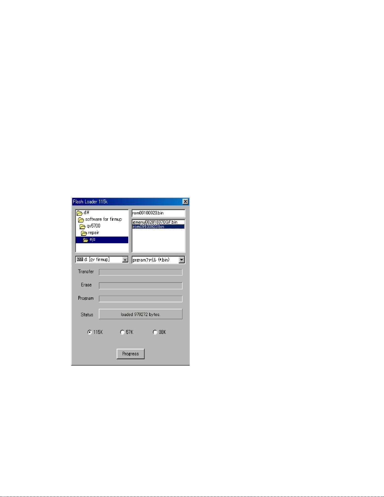
(2) Boot FLASH LOADER "Fload115.exe." and select the transmission files.
• The transmission files are "rom09100923.bin" and "gmenu08281837EGF.bin".
• Select and rewrite the files one by one.
• After the transmission file is selected, "loaded*****bytes."appears on the "Status" column of the display .
When "rom09100923.bin" is selected, "loaded 979272 bytes."appears.
When "gmenu08281837EGF.bin" is selected, "loaded 894428 bytes." appears.
(3) Extract the CF card from the camera unit.
(4) Connect the RS-232C cable between the camera and the PC.
(5) Click "Progress" button on FLASH LOADER "Fload115.exe." of the PC.
At this time, keep the camera power off.
(6) Insert the AC adapter and turn the power on.
• Since the software is damaged in most cases, the camera turns on automatically as the AC adapter
is connected. In such case, keep the power switch "off" as the progress bar on the FLASH LOADER
"Fload115.exe." starts to move.
• If the progress bar does not start moving, turn the power switch to "PLAY".
(7) The progress bar on FLASH LOADER "Fload115.exe" starts to move.
• It proceeds from "Transfer" - "Erase" - "Program".
• If the camera does not turn on for a long time after clicking the "Progress" button, "read timeout"
appears on "Status" column and rewriting cannot be done.
In such case, repeat the procedures from step 1.
— 5 —
Page 8
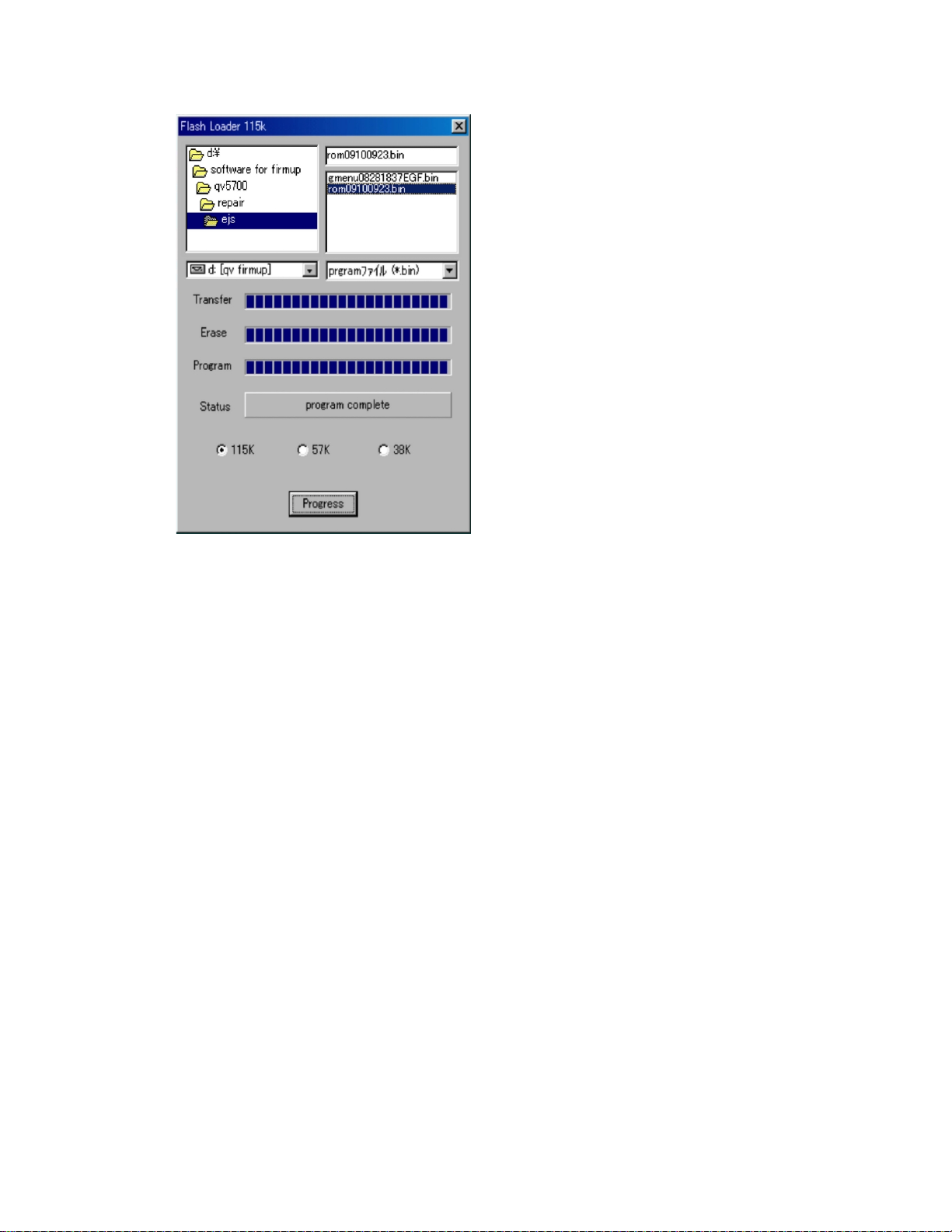
(8) When rewriting is complete, "program complete" appears on "Status" column of the display.
(9) Disconnect the AC adapter and turn off the power.
• The key operation does not turn the power off.
Disconnect the AC adapter to shut the camera off compulsorily.
(10)Next, select and rewrite the other transmission file. Repeat the above steps 1 to 8 to rewrite it.
(1 1)After both files are rewritten, disconnect QV serial cable from the camera unit and check the versions.
Turn the power switch to "PLAY" while pressing "DISP" and "MENU" to enter the test mode, and
confirm the versions of the program and GMENU.
• The versions should be changed as follows;
PROG : 02.09.10.09.23
GMENU : 02.08.28.18.37
(12)After checking the versions, take one test picture to make sure that shooting, playing back and deleting
are done normally.
— 6 —
Page 9

TEST MODE
Note: Do not perform the menu item unless explained here. (It may damage the internal data and
camera becomes unusable.)
1. Booting
To boot the test mode;
Turn the camera on while pressing MENU and DISP buttons.
To boot MENU1
Press DISP ➜ DISP ➜ MENU keys in order rapidly.
To boot MENU2
Press FLASH ➜ FLASH ➜ MENU keys in order rapidly.
To boot MENU3
Press SELF ➜ SELF ➜ MENU keys in order rapidly.
* To execute
Move up or down the control key to select a test item then press shutter button to execute it.
2. Item for testing
1 TEST MODE
2 MENU1
TEST MODE FR NTSC
PROG 01. 09. 10. 09. 23
GMENU 01. 08. 28. 18. 37
LOADER VERSION 1.20
POWER OX3F
G-MENU EGF 1.00
ADJUSTMENT
ZOOM OK KIZU OK
WB OK ZTRACK OK
IRIS OK STROBE OK
SHUTTER OK VCOM OK
MENU 1
1. INIT, NTSC JAPANESE
2. LED+SUBLCD ON
3. INIT, NTSC ENGLISH
4. CROSS HATCH
5. ANGLE DETECT CHECK
6. INIT, PAL ENGLISH
7. COLOR BAR
8. INIT, PAL GERMAN
— 7 —
Page 10

3 MENU2
MENU2
1. NOP
2. ZOOM ADJUST
3. WB ADJUST
4. IRIS ADJUST
5. SHUTTER ADJUST
6. KIZU
7. ZTRACK ADJUST
8. STROBE ADJUST
9. VCOM ADJUST
4 MENU3
MENU3
1. HARDWARE COLORBAR
2. REC INFO
3. BATT. TEST
4. PROG+GMENU UPDATE
5. PROG UPDATE
6. GMENU UPDATE
7. CHECK SUM
8. OSD DATA CHECK
9. ERROR MESSAGE TEST
10. SDRAM CHECK
MENU3
21. SHUTTER CLOSE REC
22. CLEAR ADJUSTMENT
23. GRAY SCALE(10STEP)
24. WHITE
25. BLACK
26. 50PERCENT GRAY
MENU3
11. KEY CHECK
12. LED CHECK
13. CF CHECK
14. SUBLCD ALL ON
15. CF SPEED TEST
16. AF INFO
17. SUBLCD CHECK
18. LASTMEM CLEAR
19. NOISE CAPTURE
20. BAYER CAPTURE
— 8 —
Page 11
ADJUSTMENT
1. Color adjustment data writing
1-1. Summary
(1) QV-5700 is a high quality digital camera and makeshift adjustments cannot cover the quality of the
camera's picture.
Therefore, we have prepared set of lens ass'y that is adjusted precisely in the factory and a floppy disc
containing the lens'es adjustment data as spare parts.
(2) These adjustment data are stored in the FlashROM on Main PCB.
1-2. Repairs
It is necessary to write color adjustment data for the replacements of the following units.
(1) Lens ass'y
(2) Main PCB (when FlashROM contents can be read)
(3) Main PCB and lens ass'y (when FlashROM contents cannot be read)
1-3. To replace the lens ass'y
(1) Connect AC adaptor and PC link cable to the camera.
Note: Connect the link cable to serial port COM1.
(2) Turn the camera on to set it on PLAY mode.
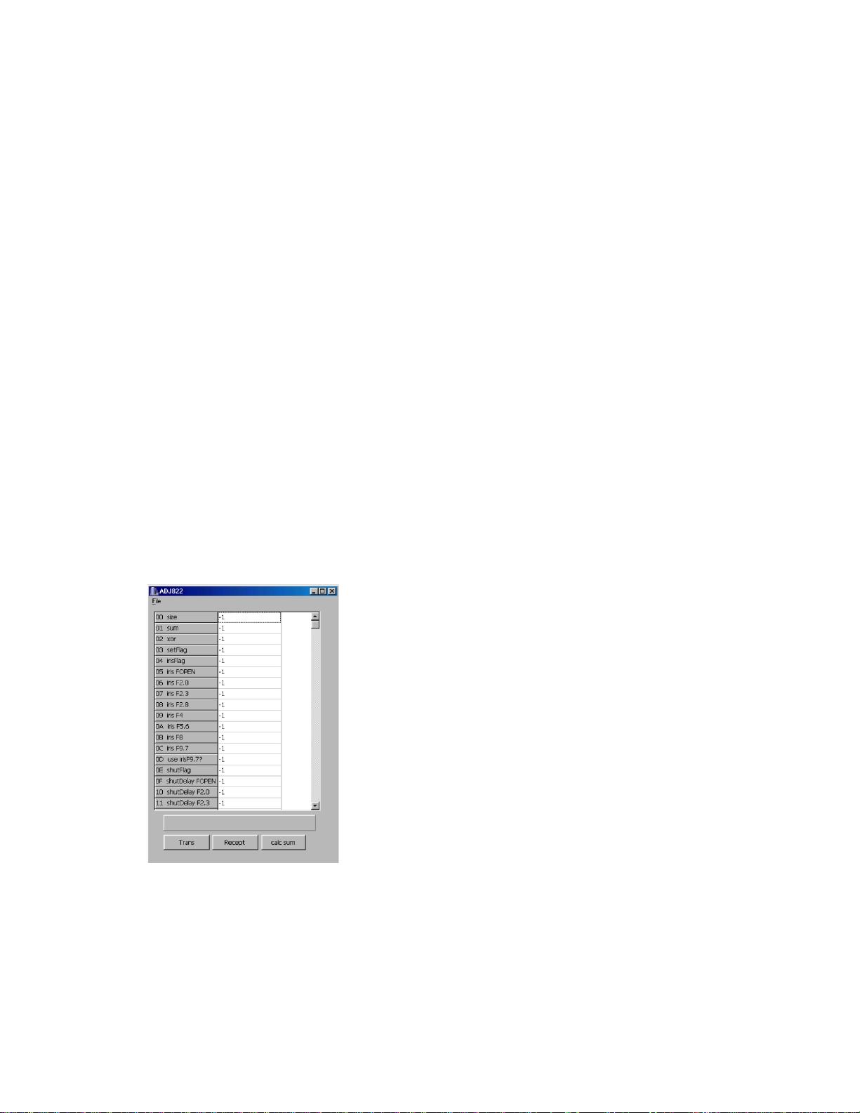
(3) Boot adjustment program ADJ822.EXE.
At this time, each adjustment data are "-1".
— 9 —
Page 12
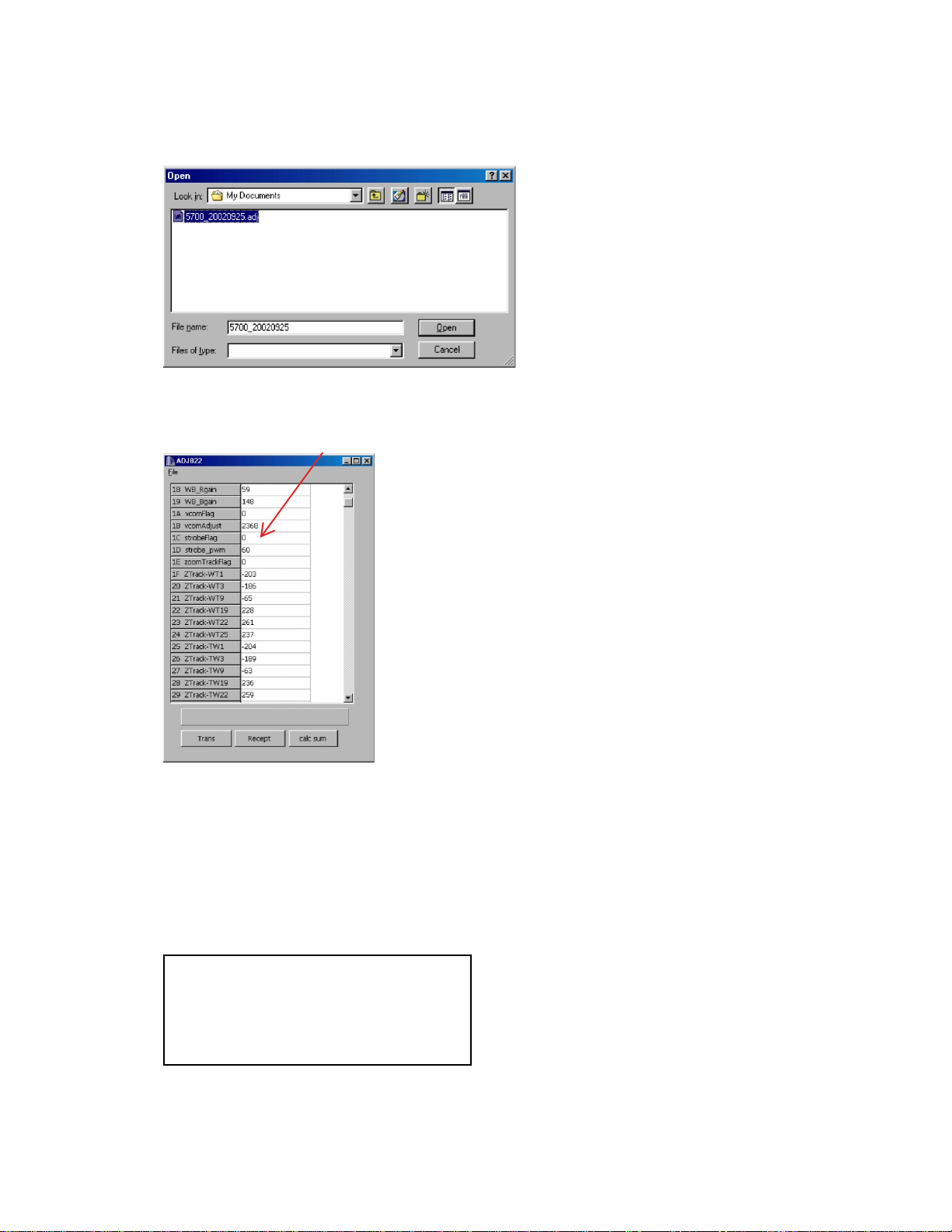
(4) Read the adjustment data of before repairs.
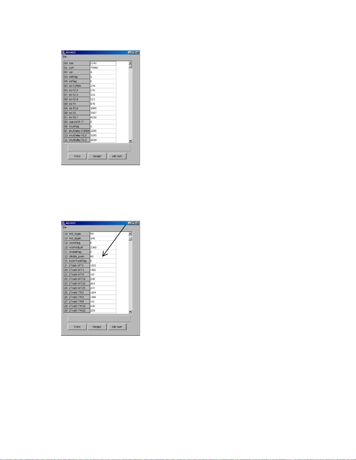
Click the Receipt button. “receive OK” will be indicated and adjustment data are shown.
Reference: At this time you can save the adjustment data in your PC.
File (F) ➜ Save as (A)
Select the drive and name the file then save it.
(Note: Do not forget to put extension code ".ADJ".)
(5) Write down the following numbers.
strobe-pwm
(6) Replace the lens ass'y.
(Adjusted in the factory and comes with adjustment data)
(7) Connect AC adaptor and PC link cable to the camera.
(8) Turn the camera on and set it on PLAY mode.
(9) Boot the adjustment program (ADJ822.EXE).
— 10 —
Page 13
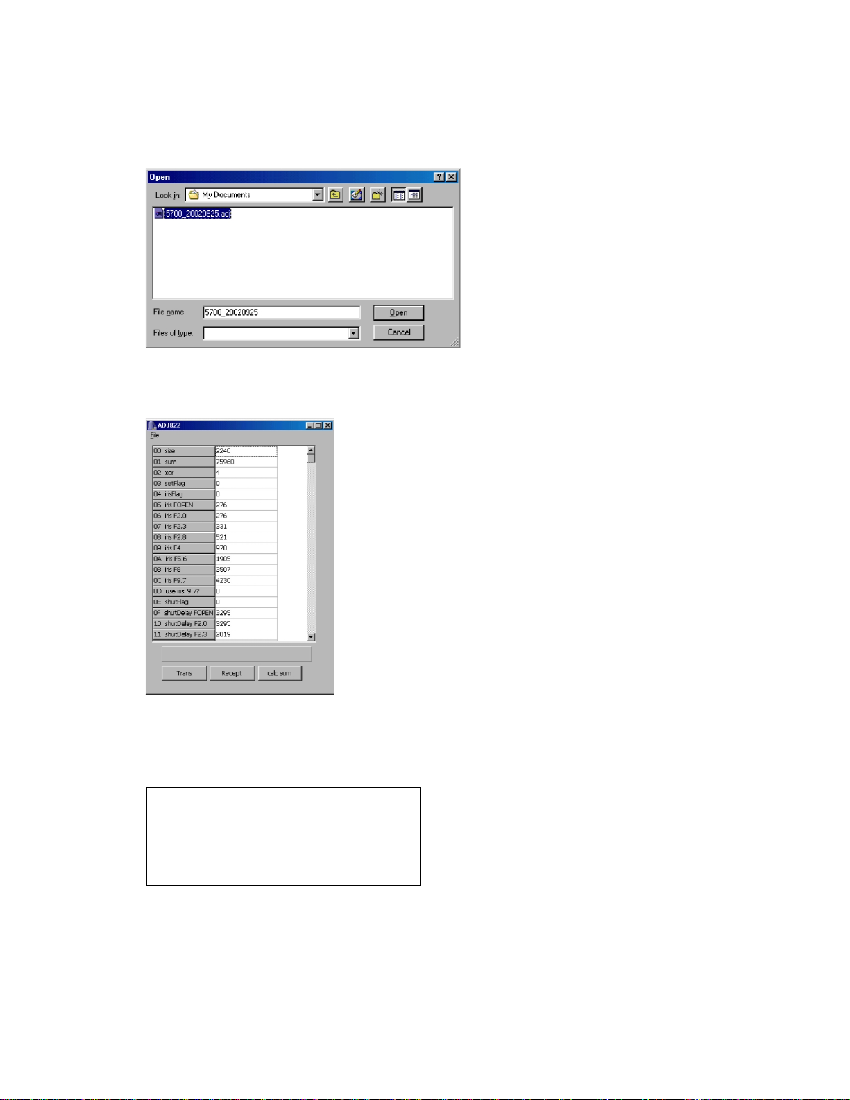
(10) Insert the floppy disc containing adjustment data of the lens ass'y in your PC and read the data.
File (F) ➜ Open (O)
Select FDD
Select adjustment data file with extension code .ADJ.
(11) Return the data of the Strobe-pwn you have written on step 5 (data before replacing the lens unit).
Set strobeFlag "0" and click the calc sum button.
Caution: Never change the other data.
(12) Transfer the data to the camera.
Click Trans button on ADJ window.
“send OK” will be shown.
(13) Turn the camera off.
(14) Booting the test mode, be sure that each adjustment item is YES.
Power on while pressing DISP and MENU keys simultaneously.
ADJUSTMENT
ZOOM OK KIZU OK
WB OK ZTRACK OK
IRIS OK STROBE OK
SHUTTER OK VCOM OK
(15) Check the camera operation by shooting a picture and play it back.
— 11 —
Page 14

1-4. To replace Main PCB (in case the contents of FlashROM can be read)
(1) Connect AC adaptor and PC link cable to the camera.
Note: Connect the link cable to serial port COM1.
(2) Turn the camera on to set it on PLAY mode.
(3) Boot adjustment program ADJ822.EXE.
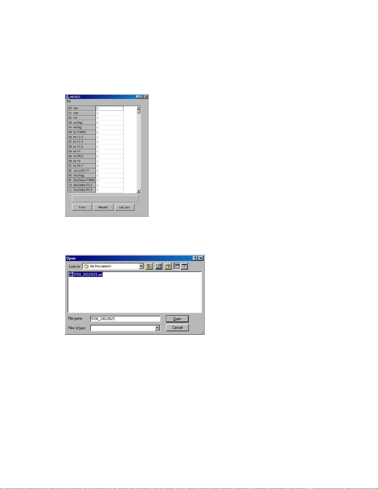
At this time, each adjustment data are "-1".
(4) Read the adjustment data of before repairs.
Click the Receipt button. "receive OK" will be indicated and adjustment data are shown.
(5) Save the adjustment data in the PC.
File (F) ➜ Save as (A)
Select a drive to save data.
Name a file name then save the data.
(It is better to name the camera's serial number as the file name.)
XXXXXXXX.ADJ (Note: do not forget the extension code .ADJ.)
(6) Replace the Main PCB
(7) Connect AC adaptor and PC link cable to the camera.
— 12 —
Page 15
(8) Turn the camera on and set it on PLAY mode.
(9) Boot the adjustment program (ADJ822.EXE).
(10) Load the saved data of the lens unit.
(11) Transfer the data to the camera.
Click Trans button on ADJ window.
“send OK” will be shown.
(12) Turn the camera off.
(13) Booting the test mode, be sure that each adjustment item is YES.
Power on while pressing DISP and MENU keys simultaneously.
ADJUSTMENT
ZOOM OK KIZU OK
WB OK ZTRACK OK
IRIS OK STROBE OK
SHUTTER OK VCOM OK
(14) Check the camera operation by shooting a picture and play it back.
— 13 —
Page 16
1-5. In case of replacing Main PCB and lens ass'y (FlashROM on Main PCB contents cannot be read)
(1) Replace PCB D and lens ass'y.
(2) Connect AC adaptor and PC link cable to the camera.
Note: Connect the link cable to serial port COM1.
(3) Turn the camera on to set it on PLAY mode.
(4) Boot adjustment program ADJ822.EXE.
At this point, adjustment data of each item is "-1".
(5) Insert the floppy disc containing adjustment data of the lens ass'y in your PC and read the data.
File (F) ➜ Open (O)
Select FDD
Select adjustment data file with extension code .ADJ.and load it.
— 14 —
Page 17

(6) Transfer the adjustment data to the camera.
Clock Trans button on ADJ program window.
Send OK. Will be shown.
(7) Turn the camera off.
(8) Booting the test mode, be sure that each adjustment item is YES.
Power on while pressing DISP and MENU keys simultaneously.
ADJUSTMENT
ZOOM OK KIZU OK
WB OK ZTRACK OK
IRIS OK STROBE OK
SHUTTER OK VCOM OK
(9) Perform the function check (Record/Playback).
— 15 —
Page 18

2. Strobe Adjustment / Strobe Operation and Recharge Current Test
1. Condition
DC in = 6.0 ± 0.1 [V]
2. Adjustment and Checking Method
1) Strobe Adjustment
1 Boot MENU2 in the test mode.
2 Select STROBE ADJUSTMENT and press the shutter release button at the dark room.
3 Adjustment is completed basically after flash is emitted four times (and the voltage of the internal PWM is
set).
Basic flashing
a) 1st flashing : Checking the amount of light in normal shooting
(emitting 4 times maximum after changing PWM value.)
b) 2nd flashing :Confirming the amount of light in the 1st flashing
(if not within the standard, confirm it again.)
c) 3rd flashing : Checking the brightness after changing PWM value
d) 4th flashing : Checking the circuit for changing aperture (F2.0 to F5.6)
2) Strobe Operation Test and Recharge Current Test
(Perform this test after the strobe adjustment.)
2-1 Strobe Recharge Current
check value: less than 1.3A
2-2 Strobe Operation Test
1 Shoot the 18% reflection sheet in the red-eye reduction mode.
(Confirm the pre-flash and the flash itself.)
2 Enter the PLAY mode and confirm the shot on the TV monitor.
3 Shoot in non-flash mode and confirm that flash does not emit light.
3. Notes and Check Value
1) There should be no image which is too light, dark or colored in 1 and 2 of the strobe operation test.
2) Do not cover the strobe sensor and the emitting part by a hand.
3) Reduce the reflection light (other than the reflection light of the 18% gray scale chart) in the upper, lower,
left, right and near (this) side of the dark room as much as possible.
4) Make sure there is no affect of the external light.
4. Block diagram
Back ground paper.
18% gray scale chart
Manufacturer : Superior
Model : Oxford gray : No.22
700mm – 50mm.
QV-5700
— 16 —
Page 19

3. Operation and Current consumption
1. Operation check
1. Unti-shock, Battery operations, AC adaptor operations
2. Switch, buttons operations
3. CF CARD insersion/eject operation, Cover open/close operation, battery cover open/close operation
4. Resolution and color repeatability check
5. AE operation, AF function, zoom operation
6. Video output, digital communication, USB function check
7. Dust and scratches on lens
8. Appearance check
9. Optical zoom finder check
10. SUB LCD display check
2. Current consumption test
Current consumption (DC IN = 6.0 ± 0.1 [V])
• Make sure that current consumption is less than 495 mA in PLAY mode.
• Make sure that current consumption is less than 680 mA in REC mode.
3. Change in the indication of the battery mark
Check that the indication of the battery mark changes as shown below in the PLAY mode.
DC IN = 5.00 ± 0.05 [V]
DC IN = 4.65 ± 0.05 [V]
— 17 —
Page 20

4. Assist light adjustment.
1. General
Perform this adjustment when you replace the assist light(LED).
2. Necessary equipment
(1) Dark room.
(2) AC adaptor.
(3) TV (With video terminal).
(4) Video cable.
3. Condition
(1) Perform the adjustment in a dark room.
(2) Distance between Lens and object is 2.0 ± 0.1m.
(3) The camera's upper case is removed.
4. Adjustment.
(1) Connect AC adaptor and video cable to the camera.
(2) Turn on the camera and enter REC mode.
(3) Set the drive mode dial in AEB mode.
(4) Move the control button UP, UP , DOWN, DOWN.
(5) Assist light (LED) comes on.
(6) To move the assist light reflected on the screen to the correct position,
turn the screw A and B as shown below.
*Make adjustment while looking at the TV monitor.
5. Screw A and B.
LED plate Figure
(1) To move the assist light to the right and left,
turn the screw A.
(2) To move the assist light up and down,
turn the screw B.
6. Adjustment process.
<Before adjustment>
Focus range
reflected on the screen.
Assist light
reflected on the screen.
Screw A
Screw B
<After adjustment>
Both are matched.
— 18 —
Page 21

DISASSEMBLE
1. Remove five screws.
a)
Screw.
b)
2. After opening CF cover, open uppercase.
3. Remove the connector.
c)
d)
Two screws.
Screw.
Screw.
4. Open the Upperr case wide.
5. Battery cover and Shaft are removed.
— 19 —
Shaft Battery cover
Page 22
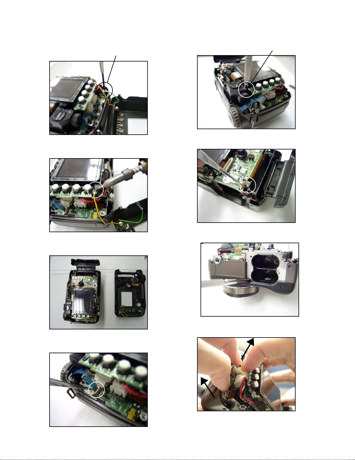
6. Remove one screw.
7. Unsolder the lead wire.
Screw.
10. Remove one screw.
11. Remove the connector (CN485)
Screw.
8. Upper case is completely separated.
9. Remove the connector (CN103).
12. Remove one screw.
13.Separate unit from the case.
*Separate the unit from JK-PCB side,
while widening the case.
— 20 —
Page 23
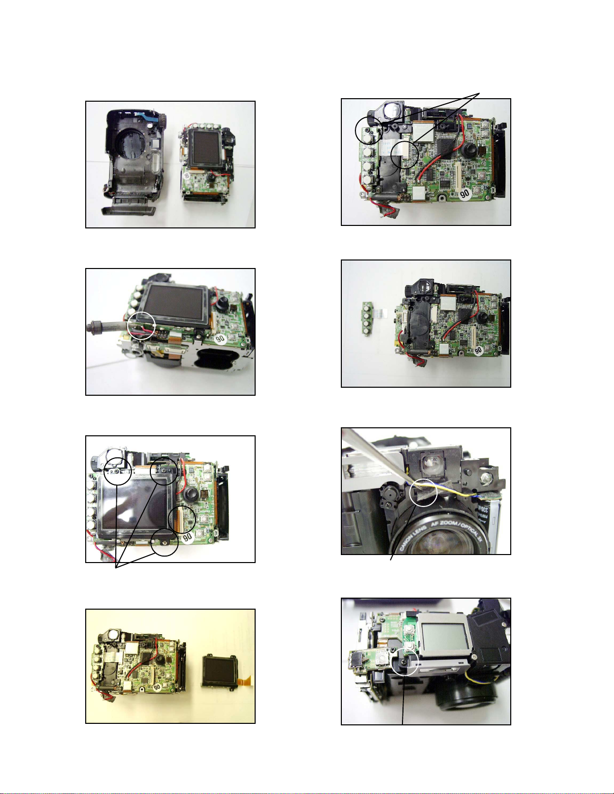
14. Separated in two blocks.
18. Remove screw and connector.
Screw.
15. Unsolder the lead wire.
16. Remove three screws and connector CN390.
19. Separate Key PCB.
20. After removing Tape, pull the wires.
Screw.
17. separate LCD unit.
Tape.
21. Remove one screw on Strobe unit.
Screw.
— 21 —
Page 24
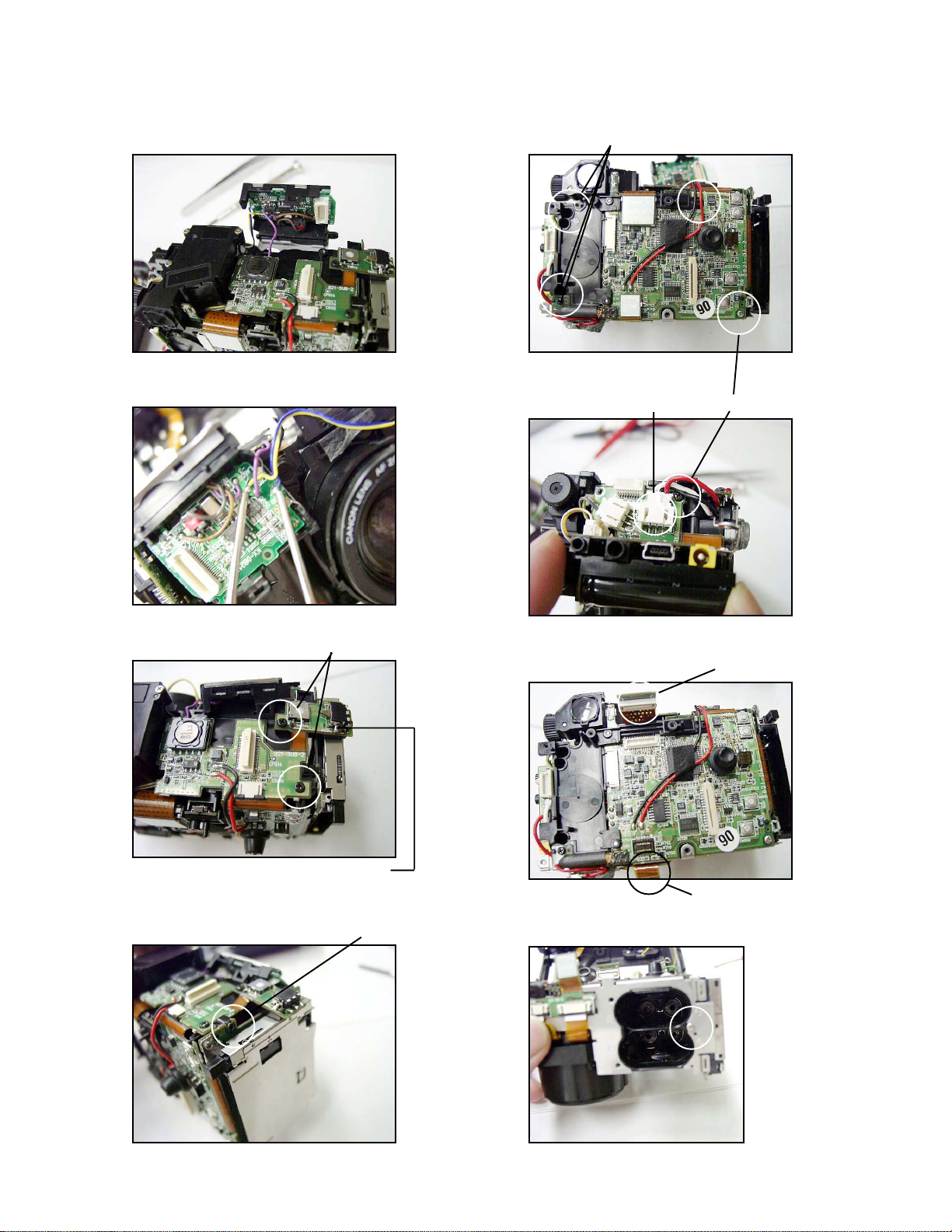
22. Open the Strobe unit.
26. Remove five screws.
Screw.
23. Discharge Fash capacitor using tool.
24. Remove two screws.
Screw.
27. Remove screw and connector.
(CN102)
28. Remove two connectors.
Screw.
CN260
*Peel off the adhesive tape attached
on the back side of the PCB.
25. Remove one screw at the side.
29. Remove one screw.
CN707
Screw.
— 22 —
Page 25

30. Remove connector (CN601).
33. Remove two screws.
31. Open Main PCB assy.
a)
b) Main PCB is open.
Screw.
34. Separate chassis.
35. Remove one screw.
32. Remove three screws and two connectors
CN705, CN706.
Screw.
Screw.
36. Remove JK-PCB
— 23 —
Page 26

37. Remove two screws.
Screw.
39. Remove Lens unit.
38. Remove one screw.
Screw.
■ Tool
Soldering iron / solder / desoldering wire
Precision screwdrivers / T weezers
Discharge tool (Resistor 1.5 kΩ 5 W) / Pliers
40. Lens unit is separated.
— 24 —
Page 27
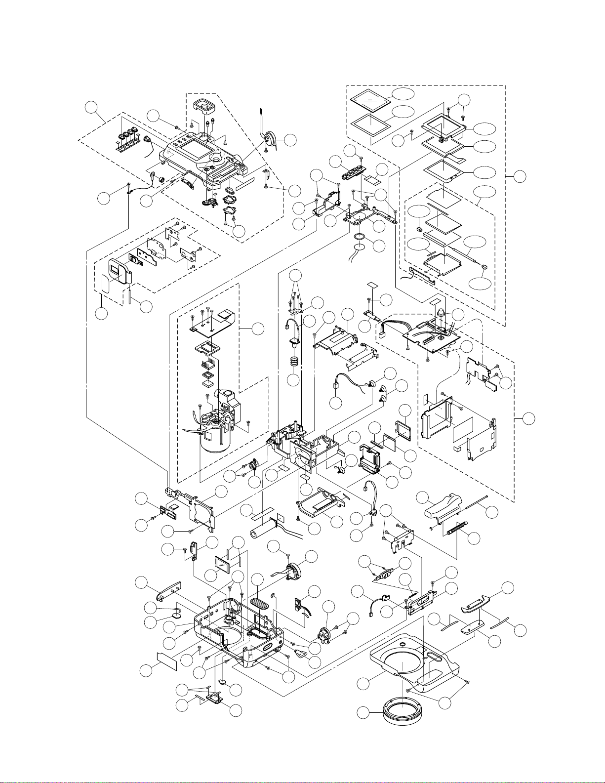
EXPLODED VIEW
13
S1
9
S4
10
S3
S6
(+3.5 FD)
2-1
2-2
14
S7
4
S7
S6
S1
S7
5
S7
44
51
S7
1
6
45
40
52
48
S7
39
S7
2-9
2-7
S7
58
42
11
S7
S7
2-8
2-9
2-3
2-4
2-5
2-6
2
S7
S1
15
57
55
49
59
65
47
20
41
S4
S4
43
24
S7
18
S3
25
23
50
46
S7
38
8
S6
31
17
S7
26 62
19
S4
60
S2
28
30
7
S7
S4
64
16
29
S4
S2
12
61
27
S6
S4
56
53
S7
37
36
54
32
63
S5
S4
33
3
34
35
21
63
22
— 25 —
Page 28

PARTS PRICE LIST
QV-5700
N Item Parts Code Parts Name Specification QTY Price R Remarks
Code
N11009 8394
LENS UNIT
RJK502360*002V04TK
1EQAN2
1009 8395
ASSY / DISPLAY
RJK502023*002V01TK
1DOA
2-1
1006 0534
PANEL / DP
RJK502026-001V01
1AJC
2-2
1006 0535
TAPE / DOUBLE SIDE
RJK502147-001V01
1AAX
2-3
1005 6850
FRAME /DP
RJK502087-001V01
1ACX
2-4
1002 8706
LCD
COD18T1029FN
1DEA
2-5
1006 0533
SHEET / SPACER
RJK502025-001V01
1AAX
2-6
1006 1979
BL UNIT
RJK502024*001V01TK
1BUA
2-7
1001 9241
TAPE / DOUBLE SIDE
K441932-4
1AAX
2-8
3851 2113
LAMP / FLUORESCENT
CAS-1.8JS1.8-1
1AWA
2-9
6613 5260
CAP / SILICON
K441448-1
2ABXN3
1009 8398
PCB ASSY / MAIN
RJK501949*002V05TK
1EHAN4
1009 8396
PCB ASSY / KEY
RJK503914*005V01TK
1BVBN5
1009 8397
PCB ASSY / JK
RJK501950*002V02TK
1CMAN6
1009 8399
PCB ASSY / LED
RJK502345*002V01TK
1BNBN7
1009 8400
PCB ASSY / CN
RJK503914*004V01TK
1BNBN8
1009 8401
PCB ASSY / CFSW
RJK502369*002V01TK
1BRB-9
1006 1974
ASSY / BATTERYCOVER
RJK502016*001V01TK
1BJA-10
1006 0567
SHAFT
RJK502019-001V01
1AFA-11
1005 6840
KEY / CURSOR A
RJK502058-001V01
1ACBN12
1009 7601
PLATE / RATING
RJK502260-003V01
1AAXN13
1009 7602
SUB ASSY / UPPER CASE
RJK502473*003V04
1CEB141006 0470
SW UNIT
IB-DC-Y0535
1BJB151005 6828
COVER / CONNECTOR
RJK502075-001V01
1AFC161005 6832
COVER / AF
RJK502080-001V01
1ACX171006 0491
RING / CAM
RJK502088-001V01
1BOX181005 6839
BUTTON / MODE
RJK502057-001V01
1ARC191005 6845
PLATE / SDP
RJK502082-001V01
1AGX201006 0481
LENS / ST
CO-821STL
1AFX211006 0494
GRIP
RJK502073-002V01
1ARX221005 6827
GRIP
RJK502074-001V01
1APX231006 1978
ASSY / SHATTER]
RJK502069*001V01TK
1BDX241006 0482
SWITCH UNIT
IB-DC-Y0536
1CAB251006 4431
PIN / STRAP
RJK502474-001V01
1AKB261006 0484
STRAP
RJK502004-001V01
1AFB271006 9272
CUSHION
RJK502378-001V01
1AAX281005 6831
COVER / SENSOR
RJK502079-001V01
1ACX291005 6815
CASE / CENTER
RJK502006-001V01
1BXX301005 6829
COVER / FINDER
RJK502077-001V01
1AKXN31
1009 7603
PANEL / REAR
RJK502076-003V02
1BTX321005 6818
COVER / CF
RJK502064-001V01
1AXX331005 6820
CF UNIT
RJK502066-001V01
1AEX341006 0512
SHAFT
RJK501999-001V01
1AIX351005 6830
COVER / SHAFT
RJK502078-001V01
1AEX361006 0513
SPRING
RJK502002-001V01
1AAX371005 6819
LEVER / CF
RJK502065-001V01
1APX381006 0557
LEVER / PIN / CF
RJK502278-001V01
2ABX391006 0564
CABLE / FLAT
RJK502041-001V01
1ADX403012 1624
TRANSFORMER/INVERTER
BLT1.8K713
1ASX416601 1700
TAPE
K4117-3
3AAX421006 0500
SPRING / BATTERY
RJK502031-001V01
1ACX431006 0509
LABEL / BATTERY
RJK502306-001V01
1AAX441006 0501
CLAMP PLATE / LED
RJK502032-001V01
1ADX
- 26 -
Page 29

N Item Parts Code Parts Name Specification QTY Price R Remarks
Code
45
1006 0508
SPRING / LED
RJK502100-001V01
1ABXN46
1006 5900
UNIT/STROBE SENSOR
CO-821SU
1AXX471006 0503
SCREW / STAND
RJK502034-001V01
1AFX481006 0561
BUZZER
7BB-15-6A38
1AGX491005 6833
FRAME / A
RJK502081-001V01
1ANX501005 6847
FRAME / B
RJK502084-001V01
1ADX511005 6848
FRAME / C
RJK502085-001V01
1ADX521005 6846
FRAME / D
RJK502083-001V01
1ACX531006 0542
CASE / S
RJK502038-001V01
1ABX541006 2827
LCD
WK-TZB271-RG-B
1AIC551006 0543
CONNECTOR
RJK502338-001V01
1AAX561005 5233
STROBE UNIT
CO-821
1CEA571006 0539
HARNESS / BT
RJK502042-001V01
1ABX581006 0537
SPRING / BATTERY
RJK502029-001V01
1ABX591006 0538
SPRING / BATTERY
RJK502030-001V01
1ABX601006 0540
CHASSIS
RJK502036-001V01
1AHX611006 0492
TAPE / DOUBLE SIDE
RJK502144-001V01
2AAX621001 9241
TAPE / DOUBLE SIDE
K441932-4
2AAX631006 0489
TAPE / DOUBLE SIDE
RJK502148-001V01
2AAX641006 0487
TAPE / DOUBLE SIDE
RJK502145-001V01
1AAX651001 9198
TAPE / DOUBLE SIDE
K441932-8
1AAXS11006 0565
SCREW
ST 1.7X4.0ZNC
3AAXS21006 0480
SCREW
M1.7X4.0NI
4AAXS31006 0566
SCREW
M1.7X4.0BK
2AAXS41002 5765
SCREW
BT3 1.7X4.0BK
9AAXS51006 4432
SCREW
RJK502470-001V01
2AAXS61006 0463
SCREW
BT3 1.7X3.0NI
4AAXS75861 3690
SCREW
BT3 1.7X4.0BK
23AAX
ACCESSORY
-
1006 4225
CORD / AC
CBL-K821-AC-EU
1AWX
For EU
-
1006 4226
CORD / AC
CBL-K821-AC-UK
1BMX
For UK
-
1006 4224
CORD / AC
CBL-K821-AC-JU
1ATX
For US
N-1009 7597
CD-ROM
CK822DCA01R
1AJX-1015 1507
CARD / CF(16MB)
HB289016C4XA
1DOC-1009 0421
CABLE / USB
UC-K861-LG10
1AQC-1005 1462
HOLDER / CAP
CH-K786
1AFC-1006 4223
CHARGER / BATTERY
BC-2H-WW
1CSC
For EU/UK/US
-
1006 4227
STRAP
ST-K821
1AVC-1000 6297
NICKEL BATTERY
NP-H3-1600E-SA
4AVC
For EU/UK/US
-
3816 0266
BATTERY / ALKALINE
LR6PA/2ST
2AGC
Except EU/UK/US
-
1014 8773
CORD / VIDEO
VC-K723-FC
1ALC-1006 4218
CAP / LENS
LC-K821
1AGC
- 27 -
Page 30

N Item Parts Code Parts Name Specification QTY Price R Remarks
Code
PCB-CFSW
SW400
1005 6856
SWITCH / DETECTOR
ESE18RJ02
1ADX
PCB-CN
CN707
1005 6834
CONNECTOR
53794-0208
1AIX
PCB-JK
CN100
3502 2211
CONNECTOR
53309-1890
1AFX
CN103
3502 2557
CONNECTOR
52559-0692
1ABX
CN104
3502 2585
CONNECTOR
BM02B-SRSS-TB
1ABX
JK192
1005 6836
JACK
54819-0578
1ADX
JK194
3501 8197
JACK / MINI
HSJ1169-019010
1ADX
PCB-KEY
CN861
3502 1438
CONNECTOR
52465-1891
1AFX
CN860
3502 2508
CONNECTOR
52746-2090
1ADX
SW860
1005 6858
SWITCH
EVQP1K05M
1ACX
SW861
1005 6858
SWITCH
EVQP1K05M
1ACX
SW862
1005 6858
SWITCH
EVQP1K05M
1ACX
SW863
1005 6858
SWITCH
EVQP1K05M
1ACX
PCB-MAIN
CN390
3501 9226
CONNECTOR
52559-2692
1AEX
CN480
1002 3278
CONNECTOR
55575-5026
1BRX
CN485
1006 0435
CONNECTOR
SM02B-SSR-H-TB
1ABX
CN490
3502 1410
CONNECTOR
52745-2090
1ACX
CN600
7930 0479
CONNECTOR
AXK6S40545P
1AIX
CN601
3502 2585
CONNECTOR
BM02B-SRSS-TB
1ABX
CN610
1001 5291
CONNECTOR
52745-0490
1AAX
CN701
1005 6835
CONNECTOR
54037-0207
1AFX
CN702
1005 6814
CONNECTOR
AXK640345J
1AJX
FU102
1005 6873
FUSE
FCC16132ABTP
1AAX
FU103
1005 6872
FUSE
FCC16102ABTP
1AAX
FU104
1005 6874
FUSE
FCC16202ABTP
1AAX
SW380
1004 8661
SWITCH
SPSE22
1AHX
SW810
1005 6857
SWITCH / DETECTOR
ESE24MH1T
1ADX
SW830
1001 4578
SWITCH
TSW-3D-T50
1ACX
SW890
1006 0433
SWITCH
EVQWHE50K
1ANX
SW891
1005 6859
SWITCH
EVQPLHA15
1ABX
SW892
1005 6859
SWITCH
EVQPLHA15
1ABX
SW893
1005 6859
SWITCH
EVQPLHA15
1ABX
SW894
1005 6860
SWITCH
EVQPUM02K
1ACX
SW895
1005 6859
SWITCH
EVQPLHA15
1ABX
T155
1006 4054
CONVERTER / DC-DC
CLQ52-03
1AEX
T600
1001 9089
CONVERTER / DC-DC
CLQ122-01
1AOX
- 28 -
Page 31
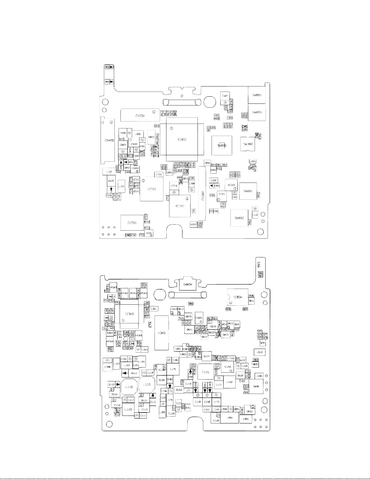
PRINTED CIRCUIT BOARDS
DA-PCB (PCB-822-MAIN-DA)
— 29 —
Page 32

DB-PCB (PCB-821-MAIN-DB)
SUB-PCB (PCB-821-MAIN-SUB)
— 30 —
Page 33
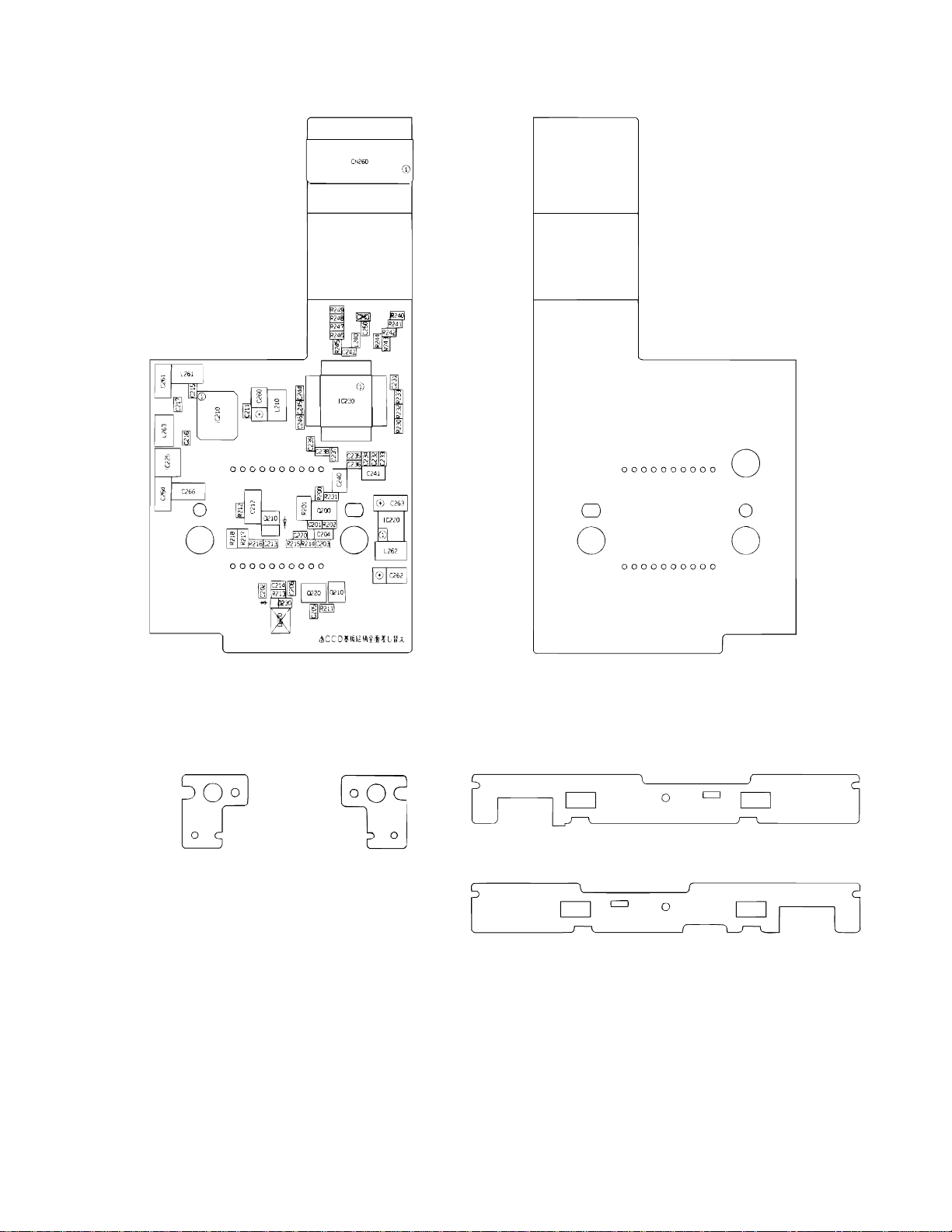
C-PCB (PCB-821-C)
BLA-PCB (PCB-821-BLA) BLB-PCB (PCB-821-BLB)
— 31 —
Page 34

CFSW-PCB (PCB-821-CFSW)
CN-PCB (PCB-821-CN)
CN707
LED-PCB (PCB-821-LED)
KEY-PCB (PCB-821-KEY)
JK-A-PCB (PCB-821-JK-A) JK-B-PCB (PCB-821-JK-B)
— 32 —
Page 35
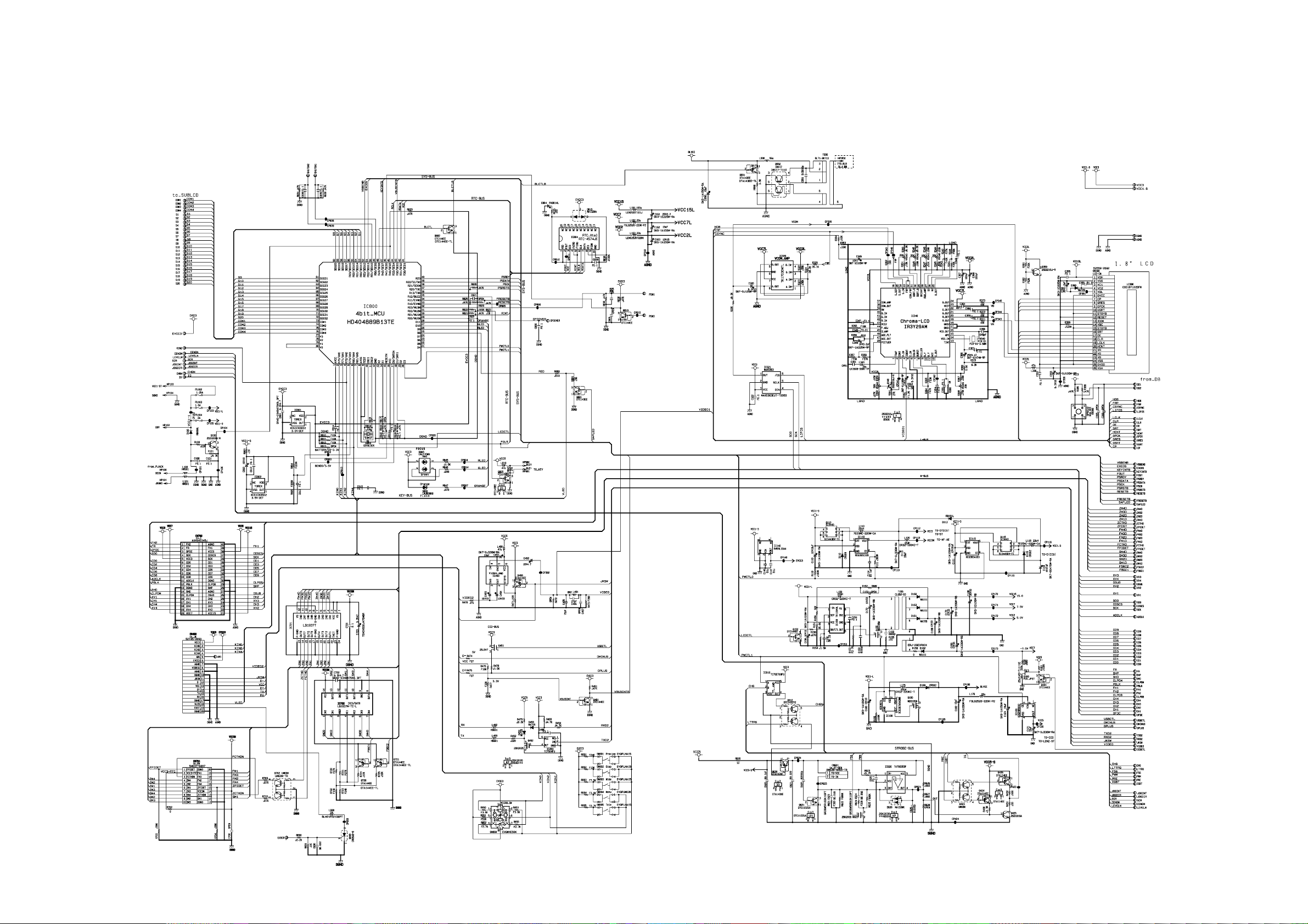
DA-PCB (PCB-822-MAIN-DA)
SCHEMATIC DIAGRAMS
— 33 —
Page 36
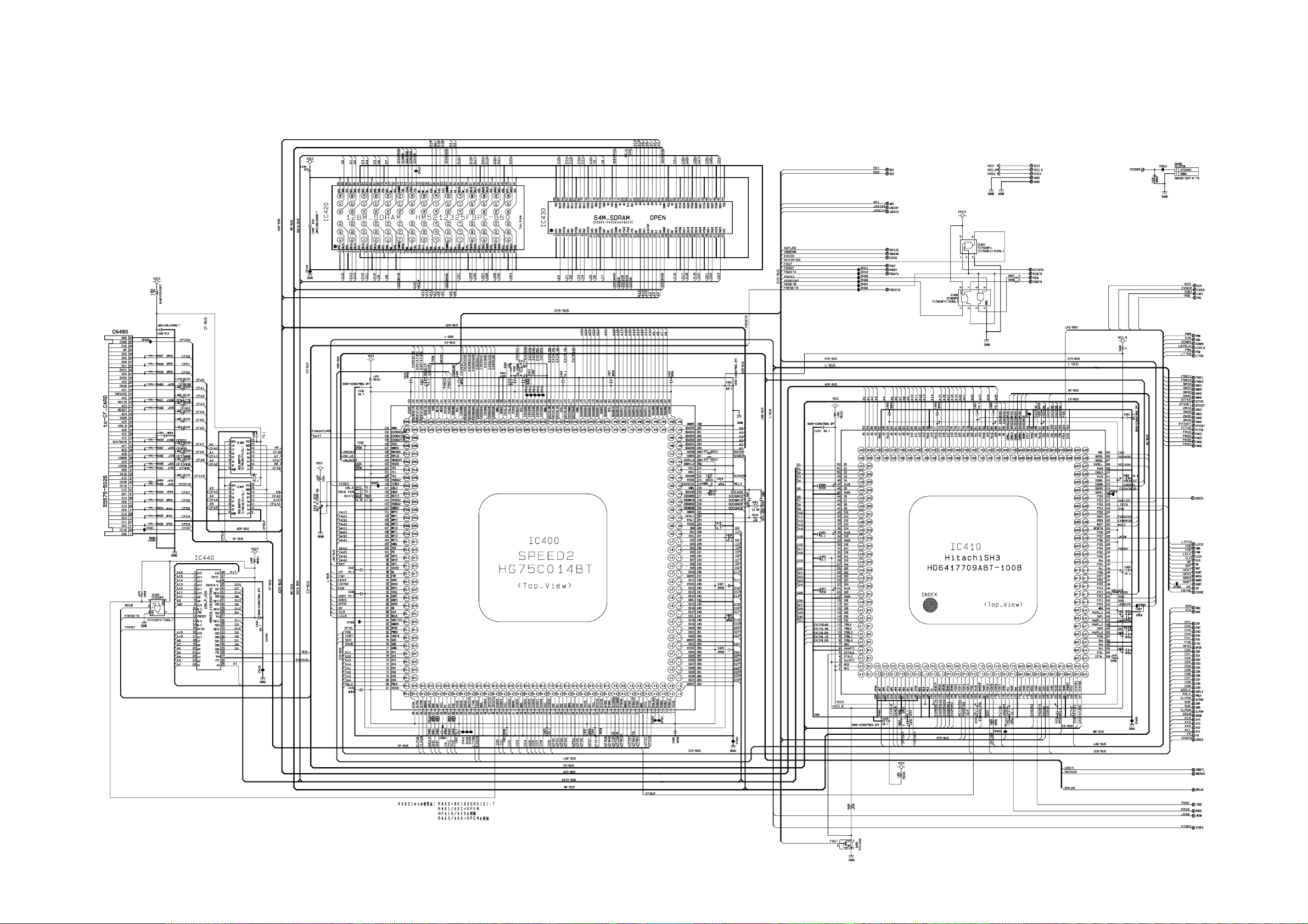
DB-PCB (PCB-821-MAIN-DB)
— 34 —
Page 37
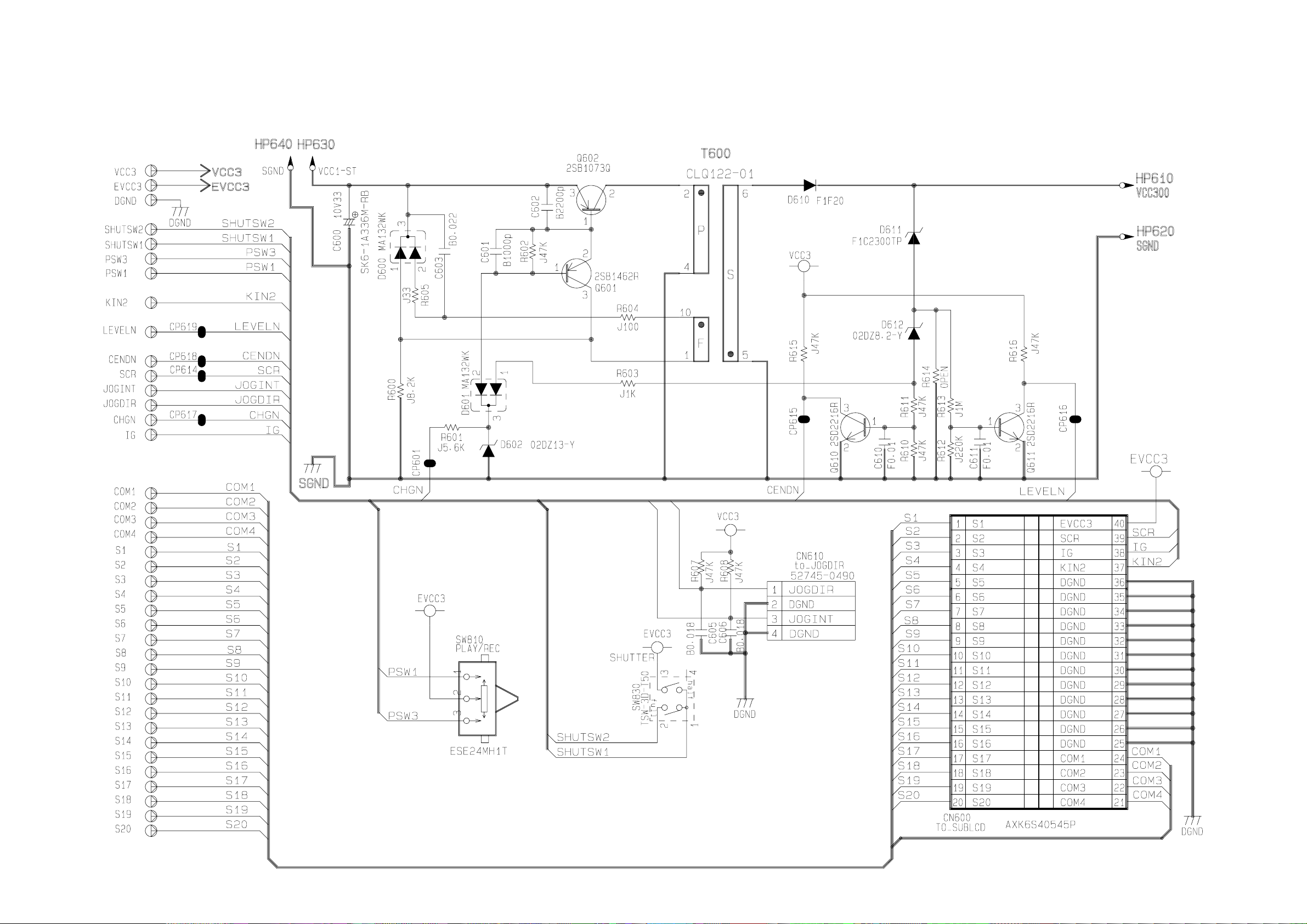
SUB-PCB (PCB-821-MAIN-SUB)
— 35 —
Page 38
C-PCB (PCB-821-C)
PBLK
CLPOB
SCK
SDO
CDSCS
CN260
to_MAIN
AXK540145J
40
AGND
39
FH1
38
VCC3C
VEE7.5C
37
36
35
34
33
32
31
30
29
28
27
26
25
24
23
22
21
VCC5
CDSCS
SCK
CD1
CD3
CD5
CD7
CD9
DGND
CLPOB
SHP
AGND
DSUB
CH2
XV3
CH3
XV2
VCC15
VCC15
LLB2520-100K-P2
L263
C264
25V_4.7u
VCC5
SCK
CLPOB
SUB
CH2
XV3
XV2
VCC15 VEE7.5
VCC3
L210
LLB2520-100K-P2
C260
6.3V_33u(A)
L261
LLB2520-100K-P2
VEE7.5
C261
10V_22u
1 2
CGND
FH2
OFDC
SD0
VCC3
CD0
CD2
CD4
CD6
CD8
ADCLK
PBLK
DGND
SHD
CLPDM
XV1
CH1
CH4
XV4
VEE7
FR
1
2
3
4
5
6
7
8
9
10
11
12
13
14
15
16
17
18
19
20
CGND
(TOREX)
2
Vin
OFDC
ADCLK
PBLK
1
Vss
3
CGND
SDOCDSCS
CD0CD1
CD2CD3
CD4CD5
CD6CD7
CD8CD9
Vout
monitor
CP200
XV1
CH1
CH4CH3
XV4
C266
25V_4.7u
IC225
XC6202PD02MR
VCC13C
VCC3
VCC5
LLB2520-100K-P2
L262
C262
6.3V_33u(A)
CD0
CD1
CD2
CD3
CD4
CD5
CD6
CD7
CD8
CD9
ADCLK
OPEN(1005_C)
XC6201P332MR
1
2
1 2
R240 10
R241 10
R242 10
R243 10
R244 10
R245 10
R246 10
R247 10
R248 10
R249 10
C251
IC220
Vin
Vss
NC3NC
(TOREX)
CGND
Vout
0
41
PBLK
RG
23
24
25
26
27
28
HBLK
R230 100
38
39
40
SCK
CLPOB
CLPDM
CLI23AVDD1
22
C24516V_0.1u
VCC3C
IC210
IV1
CH1
IV4
ISUB
IV2
CH2
37
SDI
36
SL
35
REFT
34
REFB
33
CMLEVEL
32
AVSS3
31
AVDD3
30
BYP3
29
CCDIN
28
BYP2
27
BYP1
26
AVDD2
25
AVSS2
24
C24616V_0.1u
16V_0.1u
C211
22
18
19
20
NC
NC21NC
CH3
VDC
MN3114QFN-E1
IV31CH42VH3OV74OV35NC6NC7VM
C217
16V_0.1u
C233 6.3V_1.0u
C232 6.3V_1.0u
C234 16V_0.1u
16V_0.1u
C235
C237 16V_0.1u
C238 16V_0.1u
VCC3C
CGND
17
OV415OV116OV5
0.4pitch-QFN
8
VCC3C-HD
OV8
OSUB
VHH
OV6
OV2
V-Dr
C239
16V_0.1u
VL
VEE7.5C
14
13
12
11
10
9
C241
6.3V_B4.7u
C236
16V_0.1u
16V_0.1u
16V_0.1u
VCC13C
C215
C216
C(3)
1S
(1)B E(2)
2SC3935-Q
C240
16V_B1.0u
ERJ-6GEYJ122V
V1b
V1a
V2-1
V2-2
V4-1
V4-2
V3b
V3a
R231
0
V1b
(Gb/B)
R201
V2
R202
3
2
V3b
(R/Gr)
VCC13C
0
C201
16V_0.1u
Q200
CGND
V4
(Gb/B)
C204
16V_0.47u
R200
1
47
2SC3935-Q(TX)
V1a
V2
V3a
(R/Gr)
IC200
MN39594PH-L
10
VOUT
9
PW
8
V1
7
V2
6
V3
5
V4
4
V5
3
V6
2
V7
1
V4
V8
5M-1/1.76inch CCD
(DIP) Bottom_View
C212
25V_1.0u
+33.5V?
+13V
-7.5V
VCC13C
R212
4 3
100K
16V_0.1u
A2(3)
C2(4) (1)C1
VOD
RG
BSUB
VOG
PW
VSUB
VPT
HL
H1
H2
VCC3C
2
1
C213
(2)A1
3T
RB480
VCC13C
16V_0.1u
11
12
13
C206 16V_473p
14
15
16
17
18
19
20
R2170
R2180
H2
H1
HL
D210
RB480KTL
+27 ~ 28V
+6.5 ~ 7.5V
C203
R2164.7
VEE7.5C
D230
C21450V_102p
C202
16V_0.1u
VCC13C
3
1
MA2S11100L
12
2
1
D220
OPEN
18K
R213
X(3)
3J
RB706F-40
R214
0
R215
2SD1819A-R(TX)
Q220
2
C205
3
CGND
(1)CA(2)
C220
25V_103p
1M
3
50V_102p
1
Q210
DTC143EE
C(3)
23
(2)B E(1)
DTC143EE
RG
2SD1819A
C(3)
Z
(2)B E(1)
12k
R211
4.7K
4.7K
2
R233 0
R232
C231 16V_0.1u
44
45
L240
HS241
C2426.3V_0.47u
10
11
12
C250
50V_102p
5
4
C263
6.3V_33u(A)
1 2
VCC3C-HD
48
1
D0
(LSB)
2
D1
3
D2
4
D3
5
D4
6
DVSS3
7
AD9847AKST-REEL
DVDD3
8
D5
9
D6
D7
D8
(MSB)
D9
H113DVSS115DVDD116H317DVSS219RG20DVDD221AVSS1
14
H2
H1
46
NC47NC
HD
DVSS4
DVDD4
IC230
CDS/AD
0.5pitch-QFP
H2
C24416V_0.1u
HL
43
42
VD
H4
18
CH2
XV1
CH1
XV2
SUB
XV4
CH4
XV3
CH3
OFDC
— 36 —
CGND
Page 39
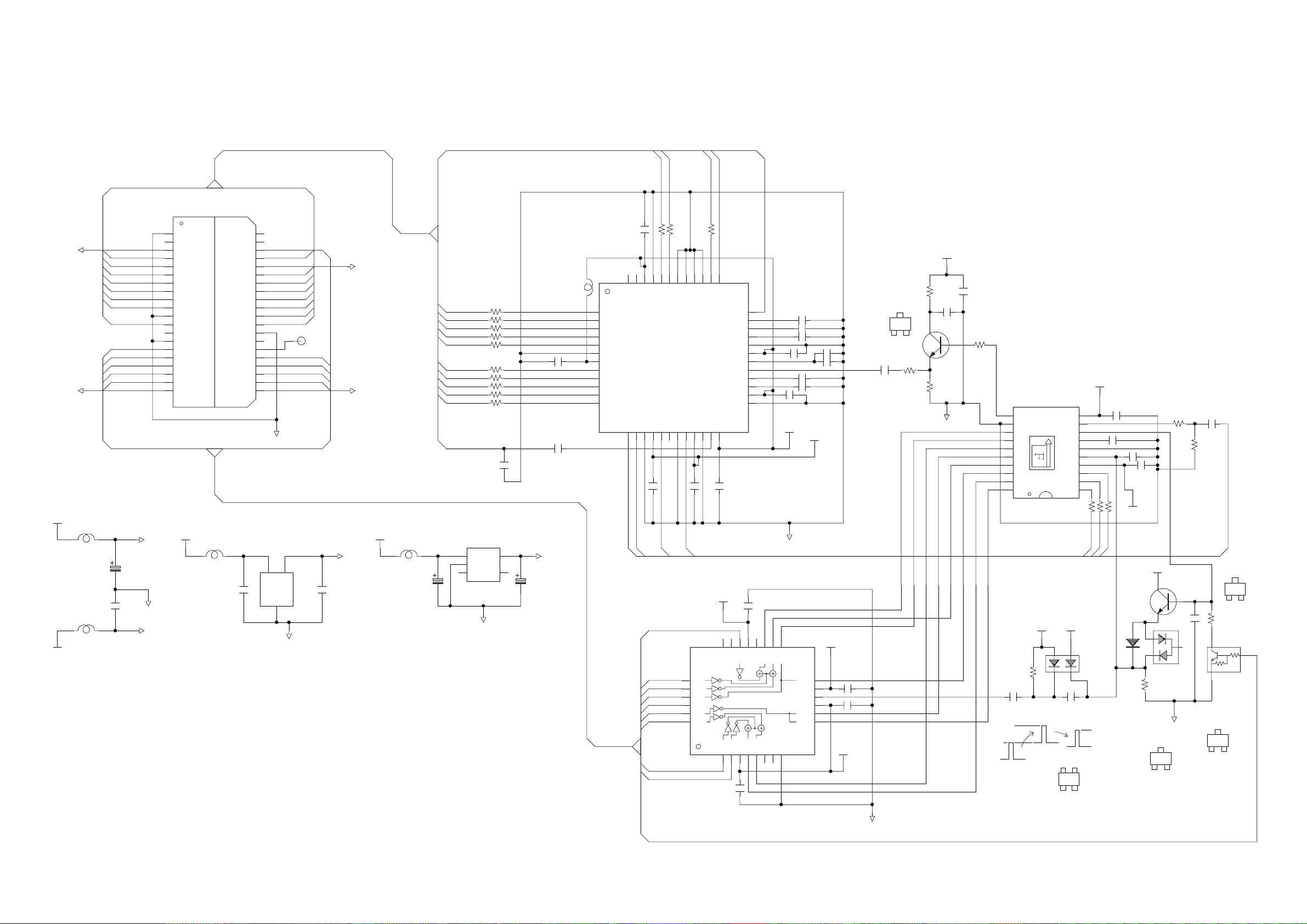
JK-PCB (PCB-821-JK)
— 37 —
Page 40

BL-PCB (PCB-821-BL)
CFS-PCB (PCB-821-CFS)
LED-PCB (PCB-821-LED)
— 38 —
Page 41
CN-PCB (PCB-821-CN)
— 39 —
Page 42

KEY-PCB (PCB-821-KEY)
— 40 —
Page 43

Ver. 1 : Correction of page 11.
CASIO TECHNO CO.,LTD.
Overseas Service Division
Nishi-Shinjuku Kimuraya Bldg. 1F
5-25, Nishi-Shinjuku 7-Chome
Shinjuku-ku, Tokyo 160-0023, Japan
 Loading...