

Page 1

QV-3500EX
INDEX
Ver. 1 MAR. / 2002
(KX-786)
MAR. 2001
(without price)
R
Page 2

CONTENTS
SPECIFICATIONS ....................................................................................................................................... 1
BLOCK DIAGRAM ...................................................................................................................................... 3
ADJUSTMENT ............................................................................................................................................ 4
1. Program version upgrading..............................................................................................................5
1-1. How to confirm the program (graphic menu) version.............................................................. 5
1-2. Upgrading procedure using the CompactFlash card............................................................... 5
1-3. Upgrading procedure using the PC link cable..........................................................................7
2. Test mode........................................................................................................................................... 8
2-1. Booting ......................................................................................................................................... 8
2-2. Item for testing.............................................................................................................................8
3. Product conditions .......................................................................................................................... 10
3-1. Color adjustment data writing.................................................................................................. 10
3-2. Flash adjustment ....................................................................................................................... 18
3-3. Flash operation and recharge operation................................................................................. 19
3-4. Current consumption ................................................................................................................ 20
3-5. VCOM DC adjustment................................................................................................................ 21
3-6. Operation check......................................................................................................................... 22
4. D-PCB Assy ...................................................................................................................................... 23
4-1. VCO free run frequency adjustment ........................................................................................ 23
4-2. VCOM AC adjustment and VCOM DC coarse adjustment ..................................................... 23
4-3. RGB AMP, Sub bright adjustment............................................................................................ 24
4-4. Contrast, Bright adjustments ................................................................................................... 25
4-5. Color adjustment ....................................................................................................................... 26
4-6. TINT adjustment......................................................................................................................... 27
5. PW-PCB Assy...................................................................................................................................28
5-1. VCC3, VCC3-M, VCC5, VCC7 Voltage check ........................................................................... 28
5-2. VCC15, VEE7 Voltage check..................................................................................................... 28
5-3. BL drive voltage adjustment..................................................................................................... 28
DISASSEMBLY/ASSEMBLY .................................................................................................................... 29
EXPLODED VIEW ..................................................................................................................................... 44
PARTS LIST .............................................................................................................................................. 45
PRINTED CIRCUIT BOARDS ................................................................................................................... 47
SCHEMATIC DIAGRAMS ......................................................................................................................... 53
Page 3
SPECIFICATIONS
File Format Still images (including panoramas): JPEG (Exif. Ver. 2.1)/TIFF, DCF standard (Design rule for
Camera File system), DPOF compatible
Movies: AVI (Motion JPEG)
Recording Medium CompactFlash card (Type I/II), IBM Microdrive
Recorded Image Size 2048 x 1536 pixels, 1024 x 768 pixels
Standard Memory Capacity, Number of Image Files, Computer Output Image Size (JPEG images only)
Still
Image size
(pixels)
2048
x
1536
1024
x
768
Storage Capacity Approximately 300 KB/second
Recording Time 30 seconds per movie (NORMAL)
Quality
FINE
NORMAL
ECONOMY
FINE
NORMAL
ECONOMY
File size
1.4 MB/image
1 MB/image
600 KB/image
350 KB/image
250 KB/image
150 KB/image
Movie (320 x 240 pixels)
30 seconds per movie (PAST)
8MB
memory card
5 images
6 images
11 images
19 images
27 images
43 images
Number of images
64MB
memory card
43 images
60 images
99 images
167 images
229 images
365 images
340MB
memory card
245 images
342 images
562 images
943 images
1292 images
2054 images
• The above figures are approximations only.
Image Deletion Single image; all images in a folder; all images in memory (with image protection)
Imaging Element 1/1.8-inch CCD (Total Pixels: 3.34 million, Effective Pixels; 3.24 million)
Lens F2 to 2.5; f = 7 to 21 mm (equivalent to 33 to 100 mm lens for 35 mm film)
Zoom Optical zoom, 3X; Digital zoom: 12X (in combination with optical zoom)
Image size is 1024 x 768 pixels when digital zoom is used.
Focusing Contrast-type Auto Focus (Auto Focus Mode, Macro Mode, Infinity Mode); manual focus; focus
lock, movable the focus frame
Focus Range Normal focus: 0.3 m to ∞
Macro focus: 6 cm to 30 cm (1X zoom)
9 cm to 30 cm (2X zoom)
The focusing range is the distance from the lens surface to the subject.
Exposure Control Light Metering: Multi-pattern, center point, spot by CCD
Exposure: Program AE, Shutter priority AE, Aperture priority AE, Manual
Exposure
Compensation: –2EV to +2EV (1/3EV units)
Shutter CCD electronic shutter; mechanical shutter, BULB, 60 to 1/1000 second
Aperture F2 to F8, auto switching or manual switching
White Balance Automatic, fixed (4 modes), manual switching
Self-timer 10 seconds, 2 seconds
Built-in Flash Flash Modes: AUTO, ON, OFF, Red eye reduction
Flash Range: Approximately 0.5 to 4 meters
Recording Functions One-shot, continuous, movie, panorama, landscape, night scene, portrait, self-timer, macro,
Best Shot
Monitor 1.8" TFT, low-glare color HAST LCD (122,100 pixels, 555 x 220)
Viewfinder LCD Monitor or optical viewfinder
— 1 —
Page 4
Clock Built-in quartz digital timepiece for time and date recording and storage with image data; auto
calendar up to 2049
Input/Output Terminals DIGITAL IN/OUT, USB port (special mini port), AC adaptor connector , VIDEO OUT (NTSC, PAL)
Power Supply Four AA-size alkaline or lithium batteries
Four AA-size nickel-metal hydride rechargeable batteries (NP-H3)
AC adaptor (AD-C620)
AC adaptor charger (BC-3HA)
Battery Life The values noted below indicate the number of hours before battery failure under normal operating
temperature (25 °C). These values are for reference only , and do not guarantee that any particular
set of batteries actually will provide the service life indicated. Low temperatures shorten battery
life.
Type of Operation
AA-size Alkaline
Batteries LR6
AA-size Lithium Batteries
FR6
AA-size Ni-MH Batteries
NP-H3
• The above figures are approximations only.
• The above guidelines are based on the following battery types:
Alkaline: MX1500 (AA) DURACELL ULTRA
Lithium: Energizer
• Battery life varies with brand.
Continuous recording values show the number of shots without using the flash. The number of
shots depends on use of the flash and whether flash is turned on or off.
Power Consumption Approximately 6.6 W
Dimensions 134.5(W) x 80.5(H) x 57.5(D) mm
Weight Approximately 320 g (excluding batteries)
Standard Accessories 8MB CompactFlash memory card; neck strap; lens cap; cap holder; soft case; special USB
cable; special video cable; data transfer cable; CD-ROM; four LR6 alkaline batteries; Basic
Reference; bundled software user’s manual
• This camera does not have a separate battery to power its clock. Clock settings are cleared whenever power to the camera is cut
off (by batteries going dead while the camera is not connected to an AC power outlet with the AC adaptor) for about 24 hours. After
power is resumed, either by loading fresh batteries or connecting to an AC power outlet, you will have to set the correct time and
date again.
• The liquid crystal panel built into this camera is the product of precision engineering, with a pixel yield of 99.99%. This also means,
however that 0.01% of the pixels can be expected to fail to light or to remain lit at all times.
Continuous Playback
145 minutes
270 minutes
170 minutes
Continuous Recording
35 minutes (210 shots)
150 minutes (900 shots)
110 minutes (660 shots)
— 2 —
Page 5
BLOCK DIAGRAM
KA-
PCB
TELE
WIDE
DISP
PREVIEW
SUB-LCD
SUB-PCB
51pin
RTC
RTC-4574
SUB
Microprocessor
HD404889
BACK UP
Capacitor
4.0 MHz
KB-
PCB
+,–
ENTER
MENU
3pin
4pin
80pin
CF
VCC7
(8.0V)
BLVCC
(5.4V)
VCC3
(3.3V)
DOWN
Converter
CCD/LCD
Power
VCC15
(15.0V)
VEE7
(-7.5V)
VCC5
(5.0V)
IrDA
Controller
48.0MHz
CCD-FPC
KEY
MODE TIMER MACRO
FLASH
SHUTTER(Half/Full)
BL UNIT
3pin
D-PCB
26pin
LCD Module
V
DD: 3.3V
VGH: 15.0
VGL: -15.0V
VSH: 5.0V
CDS/AGC/ADCAD9803
MPU
LR38665Y
TFT
Controller
CM7019L3
Chroma I/F
IR3Y29AM
29.5 MHz 24.0 MHz
24.5454 MHz
SDRAM
(64M X 2)
FLASH/
MASK
(16M)
EEPROM
(4K)
TGCXD2497R
36.0 MHz
5.0 MHz
MD
Microprocessor
SW
CF
Controller
6pin
16pin
19pin
CCD
LENS BLOCK
Canon
Zoom X 3
FINDER
UNIT
ICX252AQ
3.58 MHz
REG
Vertical/Horizontal
Sensor
EVCC(3.3V)
AF DRIVER
IRIS/SHUTTER
DRIVER
ZOOM DRIVER
BUS BUFFER
TC74AC367 X 2
SW-PCB
BL-PCB
VCC3-M
(3.4V)
PW-PCB
AC
Flashing
Controller
Photp
Sensor
ADPT
ST-PCB
10pin
B to B
10pin
Charging
Booster
SJ-PCB
FLASH
FOCUS
LED
SERIAL BUFFER
VIDEO DRIVER
USB TRANSCEIVER
Buzzer
REC/
PLAY /
OFF
SHUTTER
LED-PCB
SELF
LED
VCC5
(5.0V)
CF
SW
g,h
Flash
Control
Motor system
step-down
transformer
LCD booster
BL booster
Logic circuit
step-down
transformer
— 3 —
Page 6
■ Preparation
1. PC (IBM Compatible)/OS:Windows 95/98
2. Link cable.
3. Adjustment program
1) ADJ716.EXE (Color adjustment data transfer program)
2) FLOAD.EXE (Camera unit version up program)
3) 786 romXXXX.bin (Camera unit program data)
4) 786gmenugXXXX.bin (Camera unit menu display data)
5) qv3500ex.bin (Upgrade data for CF cards)
4. AC adaptor or stabilizer
5. Digital oscilloscope
6. Multimeter
7. Ammeter
8. Frequency counter
9. TV (with video terminal)
10. Video cable
ADJUSTMENT
11. Battery (battery operation/battery cover lock)
12. PC link program : Photo Loader (Communication function confirmation)
13. USB cable/USB driver (USB function confirmation)
14. Test chart (for photography check)
That which carried out color printing of picture data "CHART1.JPG" and the "CHART2.JPG".
CHART2.JPGCHART1.JPG
— 4 —
Page 7

1. Program version upgrading
In the camera unit, program and graphic menu are stored.
Please check the version and update it if the version is not updated.
There are two method of program updating; using CompactFlash card or utilizing PC link cable.
Note:
1. Be sure to use AC adaptor.
PCB D becomes unusable if power down or an error occurs during program transmission.
2. Unit using a mask cannot update the program.
1-1. How to confirm the program (graphic menu) version
1. Boot the test mode.
Turn the power on while pressing SHIFT and MENU buttons simultaneously.
2. Check the LCD display.
(Example)
TEST MODE
PROG 01. 03. 08. 10. 37 r Program version
GMENU 01. 03. 07. 10. 11 r Graphic menu version
· · · ·
1-2. Upgrading procedure using the CompactFlash card
(1) Prepare a CF card that contain QV-3500EX firmware upgrading software (qv3500ex.bin) in the root
directory.
(2) Insert the CF card in the QV-3500EX and connect AC adaptor.
(3) While pushing "SET" key, turn the power key on to "PLAY".
The following display comes out.
Version display (VER1.000 etc.) may come out on the bottom of the display.
PROGRAM UPDATE
YES
NO
(4) Using "G" or "H" keys, move the white cursor at "YES" then push "SHUTTER" key.
The following display comes out and rewriting firmware starts.
NOW LOADING
— 5 —
Page 8

(5) After a while, display shows “COMPLETE!” and the camera is set in PLAY mode.
(6) Turn the camera off then turn the power key to “PLAY” while pushing “SET” key.
Check the version number on the display.
PROGRAM UPDATE
YES
NO
VER1.001
This time “VER1.001” will be shown.
(7) If the version number is correct, the firmware upgrading is completed.
Turn the camera off.
(8) Take a test picture.
Take one picture and play it back and check the result.
If the picture is normal, delete it and complete the test.
— 6 —
Page 9

1-3. Upgrading procedure using the PC link cable
The restoration method at the time of firmware upgrade failure
(1) Set CD-ROM for Service Disc into CD-ROM drive of a personal computer and boot FLASH LOADER
“Fload.exe” then select a file to be transferred.
The transmission files are “786romXXXX.bin” and “786gmenuXXXX.bin”.
Perform file selection and rewriting one by one.
If a transmission file is chosen, “loaded ***** bytes” is shown on the “Status” column of the display.
(2) Extract CF card from the camera unit.
(3) Connect the QV serial cable between the camera and the PC.
(4) Click “Progress” button on FLASH LOADER “Fload.exe” of the PC.
At this time, keep the camera’s power off.
(5) Insert an AC adaptor and turn the power on.
Since the software is damaged in most cases therefore power turns on as soon as AC adaptor is
connected. In such a case, operation checking LED turns on in green so it does not matter even the
power key is off.
In case power does not turn on (operation checking LED does not turn on in green) when AC adaptor
is connected, turn the power key to “PLAY”.
(6) The progress bar on FLASH LOADER “Fload.exe” starts to move.
The progress bar proceeds to “Transfer”, “Erase” then “Program”.
If a camera has not been turned on for a long time after clicking the “Progress” button, “read timeout” is
shown on “Status” column and writing is not be done.
In such a case, repeat the procedures from step 1.
(7) If writing is completed, “program complete” will be shown on “Status” column of the display.
(8) Disconnect AC adapter and shut off a power supply.
This method does not turn the power off by key operation.
Therefore, disconnect the AC adaptor to shut the camera off compulsorily.
(9) Continuously choose and rewrite the other transmission file.
Repeat the above steps 1 to 8 to rewrite.
(10) When both files are rewritten, disconnect QV serial cable from the camera and check the version
indication following the undermentioned procedure.
While pushing down “DISP” and “MENU” keys, turn the power key to “PLAY” and check the version
numbers of Program and GMENU.
(11) After checking the version numbers, take one test picture and make sure that shooting, playing back,
and deleting are done normally.
— 7 —
Page 10

2. Test mode
Note: Do not perform the menu item unless explained here. (It may damage the internal data and
camera becomes unusable.)
2-1. Booting
To boot the test mode;
Turn the camera on while pressing SHIFT and MENU buttons.
To boot MENU1
Press SHIFT ➜ SHIFT ➜ MENU keys in order rapidly.
To boot MENU2
Press FLASH ➜ FLASH ➜ MENU keys in order rapidly.
To boot MENU3
Press SELF ➜ SELF ➜ MENU keys in order rapidly.
* To execute
Use + or – keys to select a test item then press shutter button to execute it.
2-2. Item for testing
1 TEST MODE
JAP + EN
01. 03. 08. 10. 37
01. 03. 07. 10. 11
0X00000009
0X00000322
STROBE
KIZU
ZOOM
FOCUS
0X27
YES
YES
YES
YES
• TEST MODE (IRDA OK)
• PROGRAM Version
• Graphic Menu Version
• Loader Version
• Motor MCU Version
• Power MCU Version
• STROBE ADJUST (Yes/No/Ng/Err)
• KIZU ADJUST (Yes/No/Ng/Err)
• ZOOM ADJUST (Yes/No/Ng/Err)
• FOCUS ADJUST (Yes/No/Ng/Err)
• CCD ADJUST 1 (Yes/No/Ng/Err)
• CCD ADJUST 2 (Yes/No/Ng/Err)
• CCD ADJUST 3 (Yes/No/Ng/Err)
TEST MODE
PROG
GMENU
LOADER
MOTOR
POWER
CCD1
CCD2
CCD3
YES
YES
YES
NOTE:
YES: When adjustments are completed. (Normal value)
NG: When adjustments are incompleted. (Abnormal value)
NO: IF adjustments are failed.
ERR: EEPROM Read Error
"NO" and "ERR" are designated as purple, "NG" as red.
"TEST MODE" is designated as green when adjustments are all completed.
"IRDA OK" appears beside TEST MODE TITLE when IRDA Master TEST is completed.
— 8 —
Page 11

2 MENU1
MENU1
INIT.NTSC JAPANESE
1.
LED+SUBLCD
2.
INIT.NTSC ENGLISH
3.
CROSS HATCH
4.
ANG DET CHECK
5.
INIT.PAL ENGLISH
6.
COLOR BAR
7.
50PERCENT GRAY
8.
INIT.PAL GERMAN
9.
3 MENU2
MENU2
CCD ADJ ALL
1.
ZOOM ADJUST
2.
CCD1 (AWB AGC)
3.
CCD2 (APATURE)
4.
CCD3 (SHUTTER)
5.
KIZU
6.
FOCUS ADJUST
7.
STOROBE ADJUST
8.
4 MENU3
MENU3 1/3
DISPLAY LENS ADJ
1.
REC INFO
2.
BA TT. TEST
3.
PROG+GMENU UPDATE
4.
PROG UPDATE
5.
GMENU UPDATE
6.
CHECK SUM
7.
OSD DATA CHECK
8.
ERROR MESSAGE CHECK
9.
SDRAM CHECK
10.
MENU3 3/3
SHUTTER CLOSE REC
21.
SHUTTER SPEED CONST
22.
GRAY SCALE (10STEP)
23.
WHITE
24.
BLACK
25.
MENU3 2/3
KEY CHECK
11.
LED CHECK
12.
CF CHECK
13.
SUB LCD CHECK
14.
CF WRITE TEST
15.
AF DATA SAVE
16.
EEPROM TEST
17.
ADJ CLEAR
18.
NOISE CAPTURE
19.
BAYER CAPTURE
20.
— 9 —
Page 12
3. Product conditions
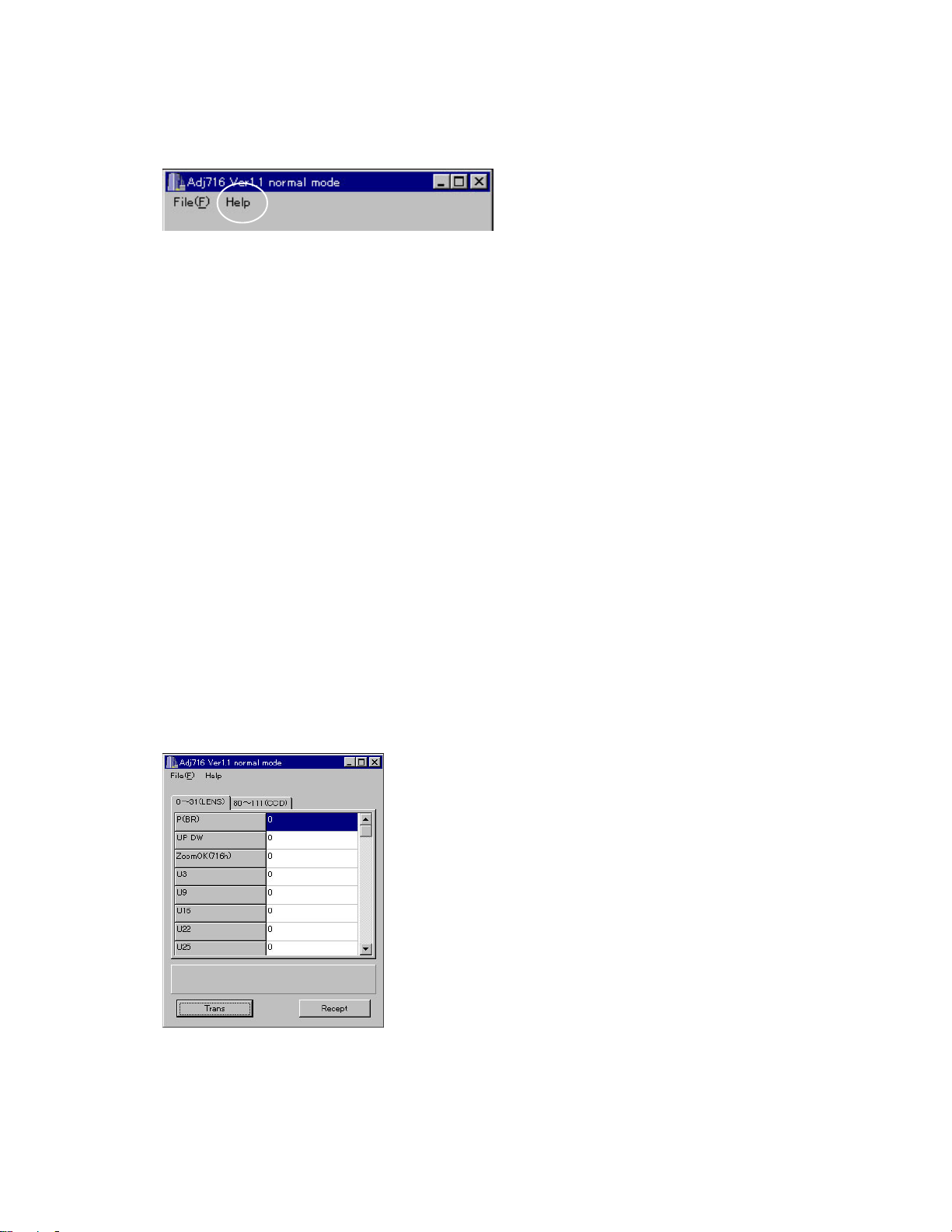
Note: Help command on adjustment window cannot be used as it uses Japanese system.
3-1. Color adjustment data writing
1. Summary
(1) QV-3500EX is a high quality digital camera and makeshift adjustments cannot cover the quality of the
camera's picture.
Therefore, we have prepared set of lens ass'y that is adjusted precisely in the factory and a floppy disc
containing the lens'es adjustment data as spare parts.
(2) These adjustment data are stored in the EEPROM on PCB D.
2. Repairs
It is necessary to write color adjustment data for the replacements of the following units.
(1) Lens ass'y
(2) PCB D (when EEPROM contents can be read)
(3) PDB D and lens ass'y (when EEPROM contents cannot be read)
3. To replace the lens ass'y
(1) Connect AC adaptor and PC link cable to the camera.
Note: Connect the link cable to serial port COM1.
(2) Turn the camera on to set it on PLAY mode.
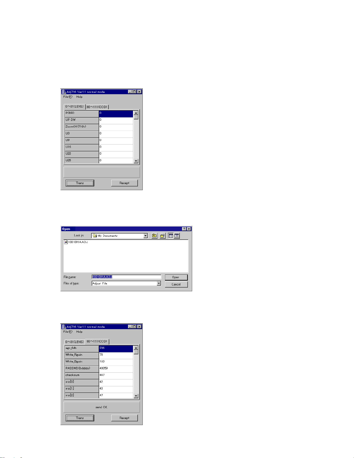
(3) Boot adjustment program ADJ716.EXE.
At this time, each adjustment data are 0.
— 10 —
Page 13
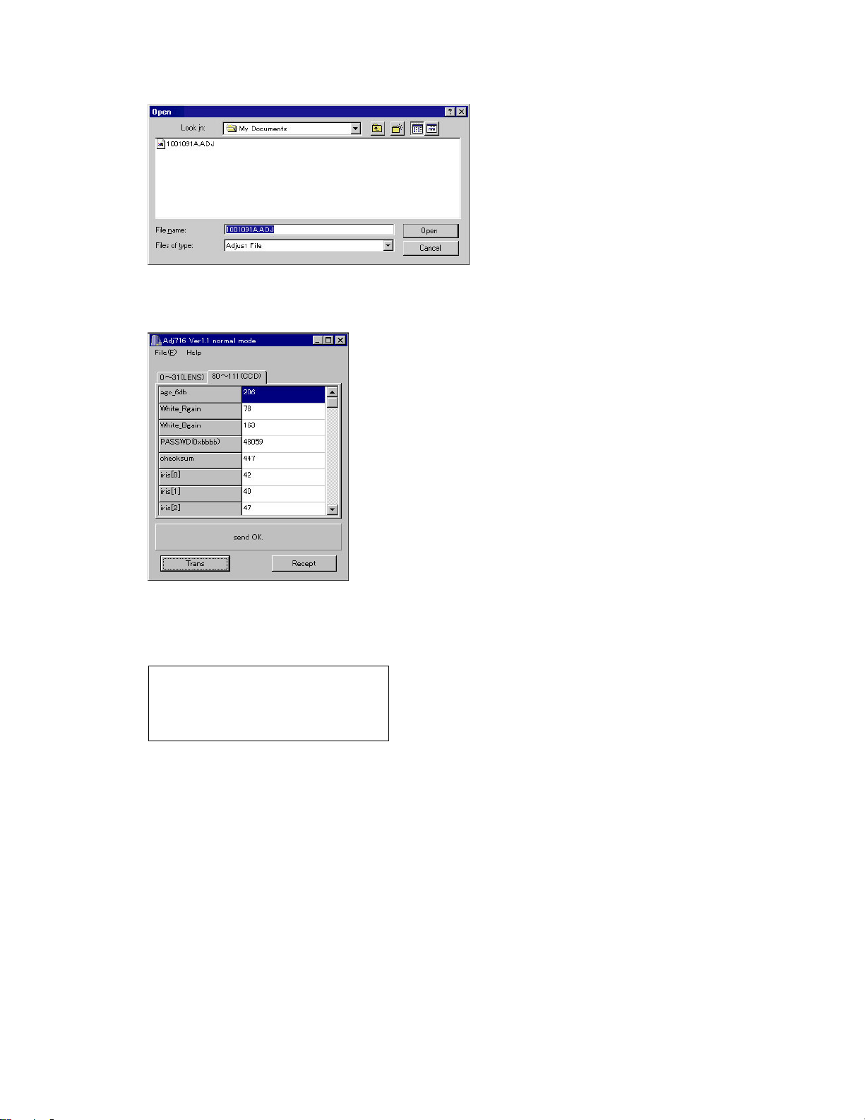
(4) Read the adjustment data of before repairs.
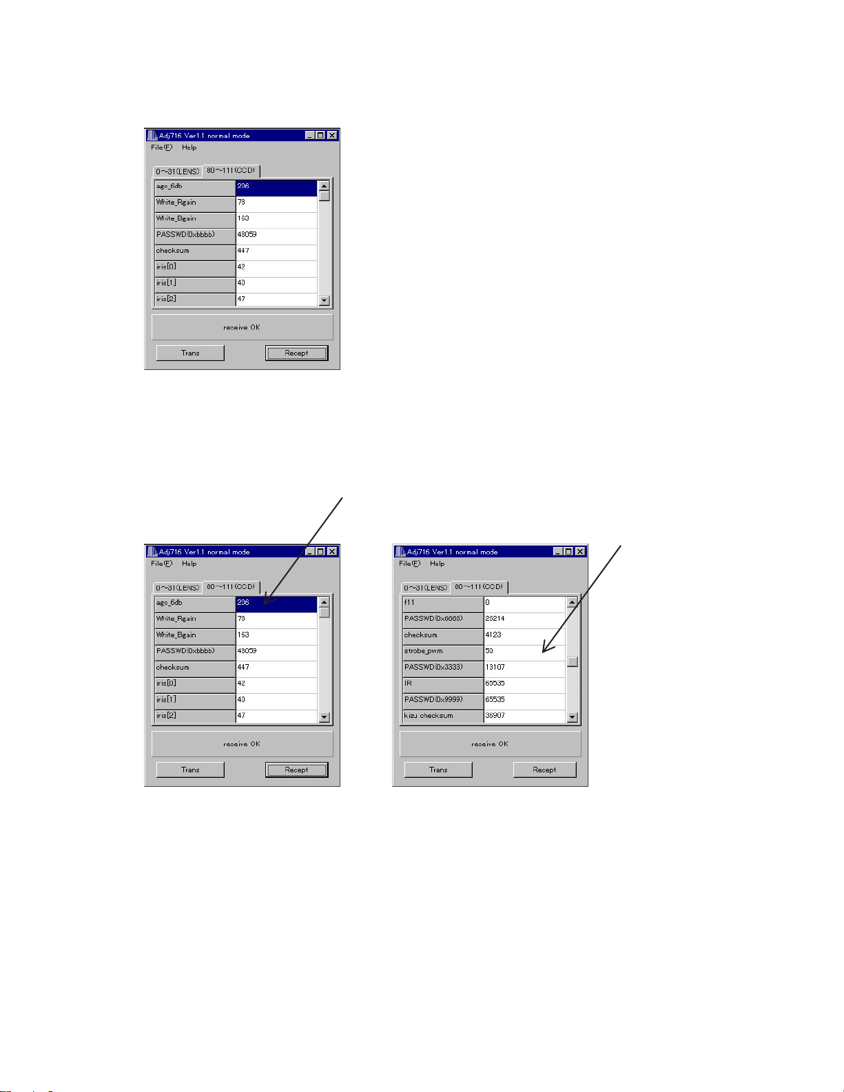
Click the Receipt button. “receive OK” will be indicated and adjustment data are shown.
Reference: At this time you can save the adjustment data in your PC.
File (F) ➜ Save as (A)
Select the drive and name the file then save it.
(Note: Do not forget to put extension code ".ADJ".)
(5) Write down the following numbers.
agc-6ab
strobe-pwm
(6) Replace the lens ass'y.
(Adjusted in the factory and comes with adjustment data)
(7) Connect AC adaptor and PC link cable to the camera.
(8) Turn the camera on and set it on PLAY mode.
(9) Boot the adjustment program (ADJ716.EXE).
— 11 —
Page 14
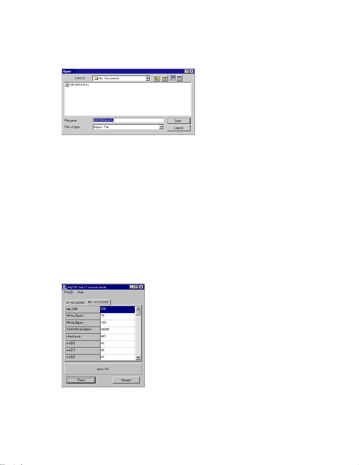
(10) Insert the floppy disc containing adjustment data of the lens ass'y in your PC and read the data.
File (F) ➜ Open (O)
Select FDD
Select adjustment data file with extension code .ADJ.
* Adjustment data file name: 9999999.ADJ
* 9999999 is the 7-digit number written on the seal stuck on the side of the lens unit.
(11) Change the following data with the number you have written on step 5 (data before replacing the lens
unit).
Caution: Never change the other data.
Agc-6db
Strobe-pwm
(12) Add the sum of three numerals agc-6db:206, white-Rgain, and white-Bgain on the checksum.
(Example) agc_6db : 206
+
white_Rgain : 78
+
white_Bgain : 163
||
checksum : 447
Note: If erroneous nuber is input, color adjustment cannot be done.
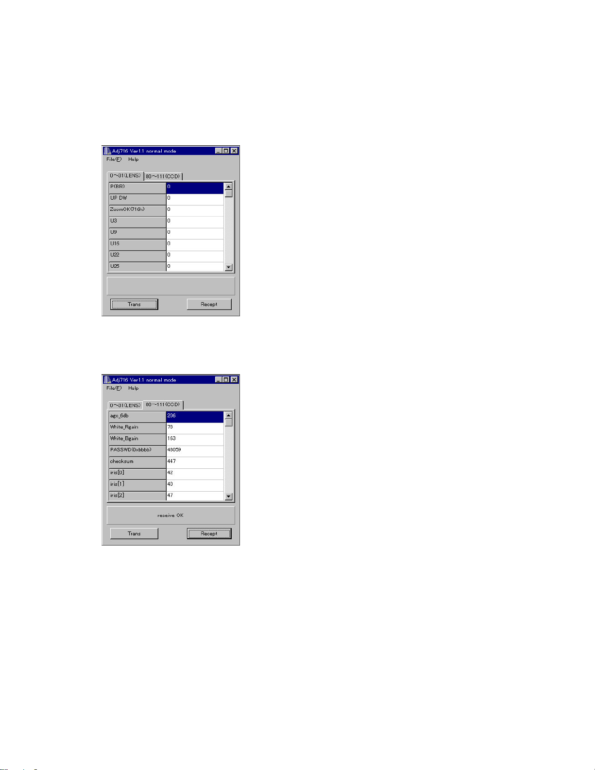
(13) Transfer the data to the camera.
Click Trans button on ADJ window.
“send OK” will be shown.
— 12 —
Page 15

(14) Turn the camera off.
(15) Booting the test mode, be sure that each adjustment item is YES.
Power on while pressing DISP and MENU keys simultaneously.
CCD1
CCD2
CCD3
YES
YES
YES
STROBE
KIZU
ZOOM
FOCUS
YES
YES
YES
YES
(16) Check the camera operation by shooting a picture and play it back.
— 13 —
Page 16
4. To replace PCB D (in case the contents of EEPROM can be read)
(1) Connect AC adaptor and PC link cable to the camera.
Note: Connect the link cable to serial port COM1.
(2) Turn the camera on to set it on PLAY mode.
(3) Boot adjustment program ADJ716.EXE.
At this time, each adjustment data are 0.
(4) Read the adjustment data of before repairs.
Click the Receipt button. "receive OK" will be indicated and adjustment data are shown.
(5) Save the adjustment data in the PC.
File (F) ➜ Save as (A)
Select a drive to save data.
Name a file name then save the data.
(It is better to name the camera's serial number as the file name.)
XXXXXXXX.ADJ (Note: do not forget the extension code .ADJ.)
(6) Replace the PCB D
(7) Connect AC adaptor and PC link cable to the camera.
(8) Turn the camera on and set it on PLAY mode.
(9) Boot the adjustment program (ADJ716.EXE).
— 14 —
Page 17
(10) Load the saved data of the lens unit.
(11) Transfer the data to the camera.
Click Trans button on ADJ window.
“send OK” will be shown.
(12) Turn the camera off.
(13) Booting the test mode, be sure that each adjustment item is YES.
Power on while pressing DISP and MENU keys simultaneously.
CCD1
CCD2
CCD3
YES
YES
YES
STROBE
KIZU
ZOOM
FOCUS
YES
YES
YES
YES
(14) Check the camera operation by shooting a picture and play it back.
— 15 —
Page 18
5. In case of replacing PCB D and lens ass'y (EEPROM on PCB D contents cannot be read)
(1) Replace PCB D and lens ass'y.
(2) Connect AC adaptor and PC link cable to the camera.
Note: Connect the link cable to serial port COM1.
(3) Turn the camera on to set it on PLAY mode.
(4) Boot adjustment program ADJ716.EXE.
At this point, adjustment data of each item is zero.
(5) Insert the floppy disc containing adjustment data of the lens ass'y in your PC and read the data.
File (F) ➜ Open (O)
Select FDD
Select adjustment data file with extension code .ADJ.and load it.
(6) Transfer the adjustment data to the camera.
Clock Trans button on ADJ program window.
Send OK. Will be shown.
— 16 —
Page 19

(7) Turn the camera off.
(8) Booting the test mode, be sure that each adjustment item is YES.
Power on while pressing DISP and MENU keys simultaneously.
CCD1
CCD2
CCD3
YES
YES
YES
STROBE
KIZU
ZOOM
FOCUS
YES
YES
YES
YES
(9) Perform the function check (Record/Playback).
(10) Perform the flash adjustment.
— 17 —
Page 20
3-2. Flash adjustment
1. General
Do not fail to perform this adjustment when you replace the flash unit.
2. Necessary equipment
(1) Dark room
(2) AC adaptor
(3) Gray paper (Superior's oxford gray No. 22)
The following sizes are available from us (also available from camra shop).
Parts code Parts name Specifications
1904 5411 Superior photographing background paper No. 22 (1.75 x 2.7m)
1904 5412 Sperior photographing background paper No. 22 (2.72 x 11m)
3. Condition
(1) Perform in a dark room.
(1) Distance between flash lens and gray paper should be 1 meter.
(1) Use lighter color of the gray paper.
Paper should be larger enough to fit in a picture taken from 1 meter distance.
(Reference; more than 1.5m x 2.0m)
4. Adjustment
(1) Connect an AC adaptor to the camera.
(2) Set the camera in REC mode.
(3) Boot the MENU2 in the test mode.
Turn the camera on while pressing SHIFT and MENU keys sumultaneously.
Press FLASH ➜ FLASH ➜ MENU in order quickly.
(4) Using + and – keys, choose STROB ADJUST and press the shutter button.
(5) When STROBE indicator appears on the right upper corner, turn the light of f then press the shutter with
the above conditions.
(6) The camera flashes more than 4 times.
(7) Confirm the following indication and turn the camera off.
EEP WR OK
PWM XX
(8) Boot the test mode.
Turn the camera on while pressing DISP and MENU keys.
(9) Make sure that STROB ADJ column is YES.
(10) Turn the camera off.
5. Block diagram
Back ground paper.
1m
REC
OFF
/
RESIZE
/
MF
PLAY
MENU
SET/ DISP
BEST SHOT
T
SHIFT
W
PREVIEW
— 18 —
Page 21

3-3. Flash operation and recharge operation
•Set QV-3500EX in “REC” mode.
•Normal Recording mode.
•Apply 6.0 ± 0.1 V voltage on DC in jack.
1. Preparation
(1) AC adaptor or stabilizer.
(2) Ammeter.
(3) TV (With video terminal).
(4) Video cable.
2. Adjustment and checking
(1) Shoot a picture with flash OFF. (Make sure there is no flash)
(2) Shoot a picture with flash ON and make sure it flashes once.
(3) Shoot in red eye reduction mode and make sure it flashes twice.
(4) Connect QV-3500EX and TV with video cable and make sure that the pictures taken in steps (2) and
(3) are not whitish, dark or erroneously colored.
(5) Make sure that the charging current is less than 1.3 A.
3. Notes
(1) Excuete in a dark room.
(2) Shoot a colorful object as much as possible.
QV-3500EX
(With video terminal)
TV
Video cable
— 19 —
Page 22

3-4. Current consumption
•Set QV-3500EX to “PLAY” mode.
1. Preparation
(1) Voltage regulator.
(2) Ammeter.
2. Adjustment procedure
(1) Current consumption (DC in = 6.0 ± 0.1 [V])
• Make sure that current consumption is less than 560 mA in PLAY mode.
• Make sure that current consumption is less than 720 mA in REC mode.
(Flash charge current is not included)
(2) Lower the voltage from 6 V as shown below then make sure the battery warning indicator changes.
DC in = 5.0 ± 0.05 [V] (one indicator is off )
DC in = 4.65 ± 0.05 [V] (two indicators are off)
DC in = 4.35 ± 0.05 [V] (All the indicators are off)
— 20 —
Page 23

3-5. VCOM DC adjustment
1. Preparation
(1) AC adaptor or stabilizer.
(2) Photo sensor/ Photo sensor amp (C2719)/L.P.F
(3) Digital oscilloscope.
2. Adjustment and checking
(1) Turn the power on while pressing SHIFT and MENU keys simultaneously. (TEST MODE)
(2) Push SHIFT ➜ SHIFT ➜ MENU keys in order rapidly. (TEST MODE 1)
(3) Choose 50 PERCENT GRAY and execute it.
(4) Monitor the photo sensor amplifier output via a low-pass filter of cutoff frequency 60Hz.
Monitoring the oscilloscope screen, adjust VR321 to minimize 60Hz ripple waveform.
3. Notes
Perform these adjustments when you replace LCD module or PCB L.
Photo diode
S1153
Photo Sensor Amp
L.P.F
C2719
REC
OFF
/
RESIZE
/
MF
LCD
MENU
SET/ DISP
SHIFT
PREVIEW
PLAY
BEST SHOT
T
W
Oscilloscope
Minimize the
ripple components
QV-3500EX
(Reference) Easy adjustment
(1) Shot a monoscope pattern with the camera and adjust VR321 so that the best 10-step gradation is
taken.
10-step gradation
10-step gradation
Monoscope pattern
— 21 —
Page 24

3-6. Operation check
1. Preparation
(1) Batteries.
(2) AC adaptor.
(3) PC (IBM compatible)/OS:Windows 95/98.
(4) Link cable.
(5) Photo loader (program).
(6) TV (with video teminal).
(7) Video cable.
(8) USB cable/USB driver
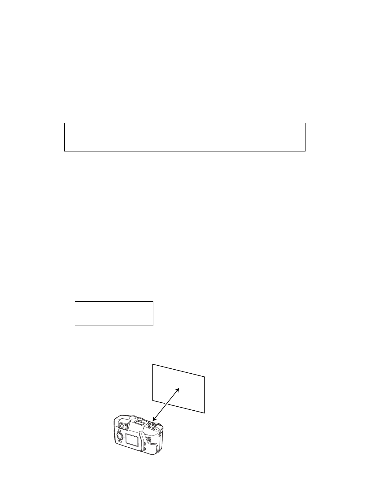
(9) Test chart (for photography check)
(That which carried out color printing of picture data "CHART1.JPG" and the "CHART2.JPG".)
2. Check matter
(1) Photography check (Please be sure to carry out.)
1 Shoot the test chart without flashing.
2 Shoot the test chart with flashing.
3 Confirm the result (compare with properly functioning camera) for;
• Color
• Focus and resolution
(2) Unti-shock check, Battery operations, AC adaptor operations
(3) Switch operation.
(4) CompactFlash insertion/pulling out movement, cover open/close operations
(5) Optical zoom finder function
(6) Sub LCD display check
(7) Resolution, color reproduction check
(8) AE function, AF function, zoom operation
(9) Video output, serial (3-pin) data transmission, USB function check
(10) Dust and scratches on lens.
(11) Appearance check
3. Note
(1) Make sure Video out setting are appropriate to your country.
(i.e. Japan=NTSC, England = PAL)
4. Test chart picture
— 22 —
CHART2.JPGCHART1.JPG
Page 25

4. D-PCB Assy
4-1. VCO free run frequency adjustment
1. Adjustment procedure
• Make sure
VCC5 (CP344) = 5.0 ± 0.05 [V]
VCC15 (CP391) = 15.0 ± 0.45 [V]
VCC7 (CP390) = 8.0 ± 0.05 [V]
VCC3 (CP220) = 3.3 ± 0.08 [V]
• Room temperature should be 20 ± 10 °C
2. Preparation
• AC adaptor or voltage regulator
• Frequency counter
3. Adjustment and checking
(1) Connect SYF (CP355) and GND (CP350).
(2) Monitor HDB (CP704) with frequency counter and adjust VR320 so that frequency becomes 15.734
± 0.1 KHz.
(3) After completing adjustment, disconnect SYF (CP7033) and GND (CP700).
4-2. VCOM AC adjustment and VCOM DC coarse adjustment
1. Adjustment procedure
• Make sure
VCC5 (CP344) = 5.0 ± 0.05 [V]
VCC15 (CP391) = 15.0 ± 0.45 [V]
VCC7 (CP390) = 8.0 ± 0.05 [V]
VCC3 (CP220) = 3.3 ± 0.08 [V]
2. Preparation
• AC adaptor or voltage regulator
• Frequency counter
3. Adjustment procedure
(1) Make sure amplitude of VCOM output (CP364) is 6.6 ± 0.3 V.
(2) Adjust VR321 so that maximum VCOM output (CP364) will be 4.8 ± 0.2 V.
4. Note
When unable to adjust using AC adaptor, use voltage regulator and supply power to be VCC1-1 (CP105)
= 5.0 ± 0.05 V.
— 23 —
Page 26

4-3. RGB AMP, Sub bright adjustment
1. Adjustment procedure
• Make sure
VCC5 (CP344) = 5.0 ± 0.05 [V]
VCC15 (CP391) = 15.0 ± 0.45 [V]
VCC7 (CP390) = 8.0 ± 0.05 [V]
VCC3 (CP220) = 3.3 ± 0.08 [V]
2. Preparation
• AC adaptor or voltage regulator
• Frequency counter
3. Adjustment and checking
(1) Turn the power on while pressing SHIFT and MENU keys simultaneously. (TEST MODE)
(2) Push SHIFT ➜ SHIFT ➜ MENU keys in order rapidly. (TEST MODE 1)
(3) Select GRAY SCALE (10STEP) and execute.
(4) Apply VCC5-1 (CP362) on the killer terminal (CP308) via 22k ohm resistor.
(5) Trigger VB waveform (CP322) by FRP (CP305) signal to adjust as noted below.
(6) Adjust RGB-AMP VR (VR302) so that VG waveform (CP322)’s pedestal-pedestal voltage is 4.30
± 0.05 Vp-p.
(7) Adjust SUB R BRIGHT VR (VR305) so that VR waveform (CP320)’s pedestal-pedestal voltage is 4.30
± 0.05 Vp-p.
(8) Adjust SUB B BRIGHT VR (VR304) so that VB waveform (CP324)’s pedestal-pedestal voltage is 4.20
± 0.05 Vp-p.
* Make sure that waveforms are not distor ted.
* Proceed to CONTRAST, BRIGHT adjustments.
Power
Supply
VCC15
VCC5
VCC7
VCC3
QV-3500EX
D-PCB
(CP391)
(CP344)
(CP390)
(CP220)
Killer terminal
(CP308)
VR(CP320)
VG(CP322)
VB(CP324)
VCC5-1
22KΩ
Digital oscilloscope
Figure 3-1
4.30 ± 0.05 or 4.20 ± 0.05V
(pedestal-pedestal)
— 24 —
3-1
Page 27

4-4. Contrast, Bright adjustments
1. Adjustment procedure
• Make sure
VCC5 (CP344) = 5.0 ± 0.05 [V]
VCC15 (CP391) = 15.0 ± 0.45 [V]
VCC7 (CP390) = 8.0 ± 0.05 [V]
VCC3 (CP220) = 3.3 ± 0.08 [V]
• RGB AMP and SUB BRIGHT adjustments should be completed (proceed from those adjustments.)
2. Preparation
• AC adaptor or voltage regulator
• Frequency counter
3. Adjustment and checking
(1) Turn the power on while pressing SHIFT and MENU keys simultaneously. (TEST MODE)
(2) Push SHIFT ➜ SHIFT ➜ MENU keys in order rapidly. (TEST MODE 1)
(3) Select GRAY SCALE (10STEP) and execute.
(4) Apply VCC2-1 (CP344) on the killer terminal (CP308) via 22k ohm resistor.
(5) Trigger VB waveform (CP322) by FRP (CP305) signal to adjust as noted below.
(6) Adjust contrast VR (VR306) so that contrast terminal voltage (CP306) is 1.50 ± 0.05 V temporary.
(7) Adjust Bright VR (VR303) so that pedestal-4th step is 2.45 ± 0.05Vp-p.
(8) Adjust Contrast VR (VR306) so that pedestal-10th step (white 100 %) is 2.90 ± 0.05Vp-p.
(9) After the adjustment, remove the 22k ohm resistor between killer terminal (CP308) and VCC5-1 (CP362).
* Make sure that waveforms are not distorted.
Power
Supply
VCC15
VCC5
VCC7
VCC3
QV-3500EX
D-PCB
(CP391)
(CP344)
(CP390)
(CP220)
Killer terminal
(CP308)
VG(CP322)
VCC5-1
22KΩ
Digital oscilloscope
Figure 3-2
2.90 ± 0.05 V
(pedestal-10 step)
— 25 —
3-2
Page 28

4-5. Color adjustment
1. Adjustment procedure
• Make sure
VCC5 (CP344) = 5.0 ± 0.05 [V]
VCC15 (CP391) = 15.0 ± 0.45 [V]
VCC7 (CP390) = 8.0 ± 0.05 [V]
VCC3 (CP220) = 3.3 ± 0.08 [V]
• Perform this adjustment after Contrast adjustment.
2. Preparation
• AC adaptor or voltage regulator
• Frequency counter
3. Adjustment and checking
(1) Turn the power on while pressing SHIFT and MENU keys simultaneously. (TEST MODE)
(2) Push SHIFT ➜ SHIFT ➜ MENU keys in order rapidly. (TEST MODE 1)
(3) Select and execute COLOR BAR.
(4) Trigger with FRP (CP305) signal.
(5) Adjust VR300 so that pulse width of 4th VB waveform (CP324) (pedestal-peak) is 2.90 ± 0.05Vp-p.
(6) Proceed to TINT adjustment.
4. Note
Perform the adjustment after (continuously from) Color adjustment.
QV-3500EX
D-PCB
(CP391)
(CP344)
(CP390)
(CP220)
Power
Supply
VCC15
VCC5
VCC7
VCC3
VB(CP324)
Digital oscilloscope
1432
2.90 ± 0.05 [Vp-p]
— 26 —
Page 29

4-6. TINT adjustment
1. Adjustment procedure
• Make sure
VCC5 (CP344) = 5.0 ± 0.05 [V]
VCC15 (CP391) = 15.0 ± 0.45 [V]
VCC7 (CP390) = 8.0 ± 0.05 [V]
VCC3 (CP220) = 3.3 ± 0.08 [V]
• Perform this adjustment after Contrast adjustment.
2. Preparation
• AC adaptor or voltage regulator
• Frequency counter
3. Adjustment and checking
(1) Turn the power on while pressing SHIFT and MENU keys simultaneously. (TEST MODE)
(2) Push SHIFT ➜ SHIFT ➜ MENU keys in order rapidly. (TEST MODE 1)
(3) Select and execute COLOR BAR.
(4) Trigger with FRP (CP305) signal.
(5) Adjust VR301 so that potential difference between the 2nd and 4th pulses' height (pedestal-peak) (A
and B) of VB waveform (CP324) is less than 0.1Vp-p.
4. Note
Perform the adjustment after (continuously from) Color adjustment.
QV-3500EX
VCC15
VCC5
D-PCB
(CP391)
(CP344)
Power
Supply
VCC7
VCC3
(CP390)
(CP220)
VB(CP324)
Digital oscilloscope
1432
BA
— 27 —
Page 30

5. PW-PCB Assy
5-1. VCC3, VCC3-M, VCC5, VCC7 Voltage check
1. Preparation
•AC adaptor or voltage regulator
•Multimeter
2. Adjustment procedure
•Make sure
VCC3 (CP110) = 3.3 ± 0.1 [V]
VCC3-M (CP111) = 3.4 ± 0.2 [V]
VCC5 (CP115) = 5.0 ± 0.15 [V]
VCC7 (CP950) = 8.0 [V]
3. Note
When unable to adjust using AC adaptor, use voltage regulator and supply power to be VCC1-1, 2, 3 =
5.0 ± 0.05 V.
5-2. VCC15, VEE7 V oltage check
1. Preparation
+ 0.6
– 0.7
•AC adaptor or voltage regulator
•Multimeter
2. Adjustment procedure
Adjust VR100 so that VCC15 (CP118) = 15.0 ± 0.1 [V] and make sure that VEE7 (CP117) = -7.5 ± 0.2 [V].
3. Notes
When unable to adjust using AC adaptor, use voltage regulator and supply power to be VCC1-1 (CP107) =
5.0 ± 0.05 V.
5-3. BL drive voltage adjustment
1. Preparation
•AC adaptor or voltage regulator
•Multimeter
2. Adjustment procedure
Make sure that BL-VCC (CP910) is within 5.0 ± 0.05V.
3. Notes
When unable to adjust using AC adaptor, use voltage regulator and supply power to be VCC-1-1 (CP107) =
5.0 ± 0.05 V.
— 28 —
Page 31

DISASSEMBLY/ASSEMBLY
1. Put on the lens cap in order to protect scratches
on the lens.
2. Open the batter y cover and remove one screw
(BT3 panhead 1.4x3.5 black).
4. Slide the CN cover and remove one screw (BT3
flathead 1.7x3.5 black).
5-1. Remove tw o scre ws (BT3 flathead 1.7x4.0 black)
from the side of the camera.
First screw
3. Remove one screw (BT3 flathead 1.7x3.5 black)
from the bottom of the camera.
5-2. Second screw
— 29 —
Page 32

5-3. When you assemble the case, screw it while CF
cover is open for better fitting.
6-1. Open the battery cover. Open the case.
7-1. Open the case from CN cov er side. It is easier to
open while pushing the upper part of the strap
pin.
7-2. When the case opens a little, open it from the
bottom.
Be careful with the cable.
6-2. Open the case as shown on the figure.
7-3. The figure shows the opened case.
Cable
— 30 —
Page 33

8-1. Desolder the gray and blue wires from D PCB.
11. Remove the green wire (SUB PCB).
8-2. Enlarged
9. Remove the cable (D PCB/ CN550).
12. Separated Upper and Lower cases.
13-1. Remove four screws (BT3 panhead 1.7 x 5.0 Ni)
that affixing the Display ass'y.
First screw
10. Remove the cable (SUB PCB/ CN451).
13-2. Second screw
— 31 —
Page 34

13-3. Third screw
13-4. Four th screw
16-1. Disconnect three cables (D PCB).
CN706
16-2. CN705
14. Remove the cable (D PCB/ CN300).
15. Remove the cable (BL PCB/ CN900).
16-3. CN200
17-1. Disconnect four wires (D PCB).
— 32 —
Page 35

17-2. Green wire
17-3. White wire
18-1. Remove D PCB by opening it from the upper part.
Caution:
Be careful with the cable under the PCB.
18-2. When Lower case and D PCB are removed.
17-4. Black wire
17-5. Yellow wire
19-1. Remove two wires (D PCB).
19-2. Orange wire
— 33 —
Page 36

19-3. Black wire
22-2. Second screw
20. D PCB is removed from Lower case.
21. Peel off the cloth on J frame.
23. Remove J frame.
24. Disconnect cable (SJ PCB/ CN100).
22-1. Remove two screws (BT3 panhead 1.7x5.0 Ni)
from J frame.
First screw
— 34 —
25. Remove one screw (BT3 panhead 1.7 x 5.0 Ni)
from Battery frame.
Page 37

26. Remove one screw (BT3 panhead 1.4 x 3.5 Black)
from Battery frame.
27. Remove one screw (BT3 flathead 1.7 x 4.0 Blac k)
from side body.
30. Displace BB PCB.
31-1. Peel cloth tape from CCD block.
Caution:
When you assemble, set the lead wires and cloth
tape as shown on the figure below.
28. Peel the cloth tape that affix the cable.
29. Remove Battery Frame.
31-2. After the cloth tape is peeled off.
— 35 —
Page 38

32-1. Disconnect the lead wire from CCD PCB.
Caution:
Leave the other wires.
32-2. After the lead wire is removed.
33-2. Second screw
33-3. Third screw
33-1. Remove three screws (BT3 panhead 1.7 x 5.0 Ni)
which affix CL unit.
First screw
34. Remove CL unit.
35. After removal of CL unit.
— 36 —
Page 39

36-1. Discharge the capacitor for the flash via 1.5kohm,
5W resistor.
37-2. Second screw
36-2. Connect the discharging jig between negative lead
of the capacitor and check pad CP220.
37-1. Remove two screws (BT3 panhead 1.7 x 3.5
black) affixing PW PCB.
First screw
38-1. Remove two screws (BT3 panhead 1.7 x 3.5
black) from SJ PCB.
First screw
38-2. Second screw
— 37 —
39. Remove the gray lead wire from PW PCB.
Page 40

40. Disconnect cable from CN640 on PW PCB.
Caution:
Be careful for wire arrangement when you
assemble.
41. Disconnect cable from CN210 on SJ PCB.
42-2. Be careful for cable arrangement when you
assemble PCB-716D-PW unit.
42-3. Enlarged picture of CN630 on PW PCB.
42-1. Remove PW and SJ PCBs.
These two PCBs are provided as a set for spare
parts.
(PCB-716D-PW unit)
42-4. Enlarged picture of CN200 on SJ PCB.
Caution:
Incomplete insertion of the cable will break IGBT
on flash PCB.
— 38 —
Page 41

43-1. Remove three screws (BT3 panhead 1.7 x 3.5
Black) which affix Flash unit.
First screw
44. Remove Flash unit.
The 2-pin cable is not included in Flash unit.
43-2. Second screw
43-3. Third screw
45. If this IGBT (Q220) is faulty, flash may light with
full emission or light only once on red-eye mode.
46-1. Remove SW PCB pulling with pliers.
— 39 —
Page 42

46-2. After removal of SW PCB.
47. Remove one screw (BT3 flathead 1.4 x 4.0 Blac k)
from Shutter block.
49. Pull click gear off.
50. Remove REC knob, shutter button, and shutter
spring
48-1. Remove the hook.
48-2. After removal of the hook.
51-1. Remove two screws (BT3 panhead 1.7 x 3.5
Black) which affixing shutter base.
First screw
51-2. Second screw
— 40 —
Page 43

52. Remove shutter base.
56. Upper case ass'y
53. Shutter block parts
54. Remove one screw (BT3 panhead 1.7 x 3.5 Black)
which affixes ST sensor unit.
57. Disconnect gray lead wire from KA PCB.
58. Disconnect cable from CN461 on SUB PCB.
55. Remove ST sensor unit.
59. Disconnect cable from CN460 on SUB PCB.
— 41 —
Page 44

60. Disconnect cable from CN451 on SUB PCB.
63-2. LED PCB outer wire
61. Peel the cloth tape.
62. Displace SUB PCB.
64. Peel cloth tape from buzzer lead wire.
65-1. Re move four screws (BT3 panhead 1.7 x 3 Ni)
which affix KB PCB.
First screw
63-1. Remove LED PCB by unhooking tow hooks.
65-2. Second screw
— 42 —
Page 45

65-3. Third screw
66-3. Third screw
65-4. Four th screw
66-1. Remove three screws (BT3 panhead 1.7 x 3 Ni)
from KA PCB.
First screw
67. Remove KA and KB PCBs.
These PCBs are provided as a set as spare part.
(PCB-K716A-KEY unit)
68. Remove rubber key.
66-2. Second screw
69. ZOOM knob
— 43 —
Page 46

EXPLODED VIEW
2
2-1
2-2
2-9
2-3
2-8 2-9
2-4
2-5
S1
X2
(+3.5"FD)
1
S7
2-7
X4
10
3 23 28 13 24 5
S3
32
2-8
2-6
34
33
31
4
22
S4
22
X7
S7
50
29
16
27
28
35
30
S2
X2
17
26
25
22
8
S7
X2
S5
X2
7
(2/2)
37
(2/2)
21
15
36
46
S7
40
48
S7
S7
37
S7
(1/2)
49
S5
X2
S6
22
18
19
6
S5
44
X2
41
7-1
S5
X3
9
38
47
7
(1/2)
7-2
S3
X3
11 39 12 14 20 S2 43 45 42
— 44 —
Page 47

MAIN BODY COMPONENT
Common 1 EJ A
Common 1 CW B
Common 1 AC X
Common 1 AI B
Common 1 DE B
Common 1 AA X
Common 1 BV B
Common 1 AW A
Common 1 BK C
Common 2 AA X
Common 2 AA X
Common 1 EF A
Common 1 BN B
Common 1 CT B
Common 1 CS B
Common 1 DH A
Common 1 AE X
Common 1 AY X
Common 1 CY B
Common 1 AV B
Common 1 BA X
Common 1 AA X
Common 1 AD X
Common 1 AD X
Common 1 AC X
Common 1 AD X
Common 1 AC X
Common 1 AN X
Common 1 AE X
Common 1 AA X
Common 1 AG X
Common 1 AA X
Common 5 AA X
Common 1 AE X
Common 1 AF X
Common 1 AH X
Common 1 AA X
Common 1 BX X
Common 2 AG X
Common 1 AA B
Common 1 AA X
Common 1 AB X
Common 1 AD X
Common 1 AD X
Common 1 AE X
Common 1 AE X
Common 1 BV X
Common 1 BW A
Common 1 AX C
Common 1 BO X
Common 1 AC X
PARTS PRICE LIST
N Item Code No. Parts Name Specification Applicable Q Price Code R
1 1001 5687 LENS UNIT K342105*1 TK(K716)
2 1001 5690 DISPLAY ASSY K342106*1 TK(K716)
2-1 6614 4530 FRAME/DISPAY K241200-1
2-2 1001 1751 PANEL/DISPLAY K441760B-1
2-3 1001 2616 TFT-LCD MODULE COD18T1035FN
2-4 6614 4540 SPACER/BACK LIGHT K441763-1
2-5 1001 5719 BL ASSY K342102*1 TK(K716)
2-6 3851 2113 LAMP/FLUORESCENT CAS-1.8JS1.8-1
2-7 1001 5721 PCB ASSY/BACK LIGHT K442091*1 TK(K716)
2-8 6614 4230 TAPE/DOUBLE SIDE K441774-2
2-9 6614 4240 TAPE/DOUBLE SIDE K441774-3
N 3 1005 3635 PCB ASSY/DIGITAL RJK501863*001V01 TK
4 1001 5727 PCB ASSY/KEY K342098*1 TK(K716)
N 5 1005 3630 PCB ASSY/LED RJK501859*003V01 TK
N 6 1005 3633 PCB ASSY/SW RJK501859*004V01 TK
N 7 1005 3634 PCB ASSY/POWER K342100*002V06 TK
7-1 1000 8870 CABLE/FLAT K441943-1
7-2 1015 1467 EJECTOR UNIT/CF 55370-0011
N 8 1005 3628 PCB ASSY/SUB K342099*003V06 TK
N 9 1005 3632 BATTERY COVER ASSY K342097*002V02 TK
10 1001 5702 FRAME ASSY/BT K342096*1 TK(K716)
N 11 1004 8639 PLATE/RATING K442081-004V01
12 1000 8856 COVER/FD-A K441951-1
13 1000 8857 COVER/FD-B K441952-1
14 1000 8858 COVER/SENSOR K441953-1
N 15 1004 8638 GRIP K441954-002V01
16 1001 1750 PANEL/DISPLAY K441761A-1
N 17 1002 2434 BUZZER 7BB-15-6A60
N 18 1004 8640 COVER/CF RJK501820-001V01
N 19 1002 3200 LABEL/CF K441492-3
20 6611 0460 PLATE/CASIO C441170-1
N 21 1001 7425 TAPE/DOUBLE SIDE K442202A-2
22 6601 1700 SHEET/INSULATION K4117-3
N 23 1004 8637 COVER/CN K241206-003V01
24 1000 8835 CASE/FD K241308-1
N 25 1004 8625 BUTTON/MODE K341797-002V01
26 1001 2586 CUSHION K442203-1
N 27 1004 8622 CASE/UPPER RJK501814-001V01
28 1000 8852 PIN/STRAP K441949-1
29 1000 8849 KNOB/ZOOM K341852-1
30 6614 5000 RUBBER KEY K341614-1
31 6614 5060 SPRING/CS K441749-1
N 32 1001 4616 BUTTON/MENU K341606-2
N 33 1001 4617 BUTTON/SET K341607-2
N 34 1004 8621 BUTTON/CS K341608-003V01
N 35 1004 8623 BUTTON/POWER RJK501819-001V01
N 36 1004 8647 CASE/LOWER RJK501795-001V01
37 1000 8859 STROBE UNIT CO-716
38 1000 8862 STROBE SENSOR UNIT CO-716SU
N 39 1004 8646 COVER/LENS RJK501793-001V01
40 6613 1210 NUT/TRIPOD K341059-1
Notes: NEW : New registration parts
Q : Quantity used per unit
R : Rank
- 45 -
Page 48

N Item Code No. Parts Name Specification Applicable Q Price Code R
Common 1 AC X
Common 1 AG X
Common 1 AF X
Common 1 AA X
Common 1 AA X
Common 1 AB X
Common 1 AR X
Common 1 AC X
Common 1 AA X
Common 1 AA X
Common 2 AA X
Common 3 AA X
Common 4 AA X
Common 7 AA X
Common 11 AA X
Common 1 AA X
Common 10 AA X
Common 1 BK C
Common 1 AF X
Common 1 AY X
Common 1 BJ X
Common 1 AL X
Common 1 AH C
R : Rank
41 1000 8839 BASE/SHUTTER K241297-1
N 42 1004 8645 BUTTON/SHUTTER K341798-002V01
N 43 1004 8649 KNOB/REC RJK501821-001V01
44 1000 8840 GEAR/CLICK K341800-1
45 6613 9110 SPRING/SHUTTER K441649-1
46 1001 2588 HARNESS/STROBE K441994-1
47 6614 5210 PCB ASSY/BB K441743-1
48 1000 8833 FRAME K341794-1
49 1001 2597 PLATE/INTERCEPTION K441955-1
N 50 1002 1537 RING/FACING K442310-1
S1 1001 2608 SCREW PS1 1.7X2.5 NI
N S2 1002 5765 SCREW BT3 1.7X4.0 BK
N S3 1004 8635 SCREW BT3 1.7X3.5NI
S4 5112 0884 SCREW BT3 1.7X3 NI
S5 1001 2551 SCREW BT3 1.7X3.5 BK
N S6 1004 8648 SCREW BT3 1.4X4.0 BK
S7 1001 2591 SCREW BT3 1.7X5.0 NI
ACCESSORY
N Item Code No. Parts Name Specification Applicable Q Price Code R
N 1005 1466 CD-ROM CK786DCA01R Except for US 1 AK X
1015 1424 CD CARD (8 MB) HB289008C4QV Except for US 1 DF C
3502 2744 CABLE/USB 59204-2301
3816 0266 BATTERY/ALKALINE LR6PA/2ST Except for US 2 AG X
N 1005 1462 HOLDER/CAP CH-K786
N 1005 1464 STRAP ST-K786
N 1005 1463 CASE/SOFT SC-786
1015 1471 CABLE/PC-LINK LC9F-DOS-K740-L Except for US 1 BU X
1014 8773 CABLE/VIDEO VC-K723-FC
N 1005 1461 CAP/LENS LC-K786
Notes: NEW : New registration parts
Q : Quantity used per unit
- 46 -
Page 49

PRINTED CIRCUIT BOARDS
DIGITAL-PCB (PCB-786D-D)
— 47 —
Page 50

SUB-PCB (PCB-716D-SUB)
— 48 —
Page 51

POWER-PCB (PCB-716D-PW)
NOTE: The Power PCB for QV-3500EX is identical to that for QV-3000EX except that one of the parts of the
power PCB for QV-3500EX; the circuit for CF Card access lamp, is deleted.
Therefore, these two Power PCBs are not compatible each other.
— 49 —
Page 52

BACK LIGHT-PCB (PCB-716D-BL)
KEY-A-PCB (PCB-716D-KA)
— 50 —
Page 53

KEY-B-PCB (PCB-716D-KB)
SWITCH-PCB (PCB-716D-SW)
— 51 —
Page 54

FLASH-JACK-PCB (PCB-716D-SJ)
CCD-PCB (PCB-716D-CCD) LED-PCB (PCB-716D-LED)
— 52 —
Page 55

DIGITAL-PCB (PCB-K786D-DA)
SCHEMATIC DIAGRAMS
— 53 —
Page 56

DIGITAL-PCB (PCB-K786D-DB)
— 54 —
Page 57

SUB-PCB (PCB-K786D-SUB)
— 55 —
Page 58

POWER-PCB (PCB-K786D-PW)
— 56 —
Page 59

BACK LIGHT-PCB (PCB-K716D-BL)
— 57 —
Page 60

FLASH-JACK-PCB (PCB-K716D-SJ)
— 58 —
Page 61

KEY-A-PCB (PCB-K716D-KA)
— 59 —
Page 62

KEY-B-PCB (PCB-K716D-KB)
— 60 —
Page 63

SWITCH-PCB (PCB-K716D-SW)
LED-PCB (PCB-K716D-LED)
— 61 —
Page 64

CCD-PCB (PCB-K716D-CCD)
— 62 —
Page 65

Ver. 1 : Change of Page 46.
CASIO TECHNO CO.,LTD.
Overseas Service Division
Nishi-Shinjuku Kimuraya Bldg. 1F
5-25, Nishi-Shinjuku 7-Chome
Shinjuku-ku, Tokyo 160-0023, Japan
 Loading...