

Page 1
QV-2000UX
INDEX
(KX-713B)
QV-2000UX/Ir
(KX-713C/D/F)
SEP. 1999
(without price)
R
Ver.1 Dec / 1999
Page 2

CONTENTS
SPECIFICATIONS ....................................................................................................................................... 1
To distinguish the model .......................................................................................................................... 3
BLOCK DIAGRAM ...................................................................................................................................... 4
ADJUSTMENT ............................................................................................................................................ 5
1. Program version upgrading..............................................................................................................5
1-1. How to confirm the program (graphic menu) version.............................................................. 5
1-2. Upgrading procedure using the CompactFlash card............................................................... 5
1-3. Upgrading procedure using the PC link cable.......................................................................... 6
2. TEST mode ......................................................................................................................................... 8
2-1. Booting ......................................................................................................................................... 8
2-2. Item for testing.............................................................................................................................9
3. Product conditions .......................................................................................................................... 11
3-1. Color adjustment data writing.................................................................................................. 11
3-2. Flash adjustment ....................................................................................................................... 17
3-3. Flash operation and recharge operation................................................................................. 18
3-4. Current consumption ................................................................................................................ 20
3-5. VCOM DC adjustment................................................................................................................ 21
3-6. Operation check......................................................................................................................... 22
4. D-PCB Assy ...................................................................................................................................... 23
4-1. VCO free run frequency adjustment ......................................................................................... 23
4-2. VCOM AC adjustment and VCOM DC coarse adjustment ...................................................... 23
4-3. RGB AMP, Sub bright adjustment.............................................................................................24
4-4. Contrast, Bright adjustment ...................................................................................................... 25
4-5. Color adjustment ........................................................................................................................ 26
4-6. TINT adjustment.......................................................................................................................... 27
5. PW-PCB Assy...................................................................................................................................28
5-1. VCC3, VCC3-1, VCC5, VCC5-1 Voltage check.......................................................................... 28
5-2. VCC15, VEE7 Voltage check...................................................................................................... 28
5-3. VCC2, adjustment and VCC13, VCC7, VEE2 Voltage check ................................................... 29
5-4. BL drive voltage adjustment...................................................................................................... 29
6. PW-PCB Assy...................................................................................................................................30
6-1. Clock oscillation check .............................................................................................................. 30
DISASSEMBLY ......................................................................................................................................... 31
EXPLODED VIEW ..................................................................................................................................... 40
PARTS LIST .............................................................................................................................................. 41
PRINTED CIRCUIT BOARDS ................................................................................................................... 43
SCHEMATIC DIAGRAMS ......................................................................................................................... 49
Page 3
SPECIFICATIONS
Description Digital camera
Model QV-2000UX
Recorded Image File Format Still images (including panoramas): JPEG (Exif. Ver. 2.1), DCF standard (design rule for camera
file system), DPOF compatible, Movies: AVI
Recording Medium CompactFlash card (Type I/II)
Recorded Image Size 1600 x 1200 pixels, 800 x 600 pixels
Standard Memory Capacity, Static 1600 x 1200
Number of Image Files, FINE 71/8 images (850KB / image)
Computer Output Image Size NORMAL 97/9 images (600KB / image)
ECONOMY 163/15 images (350KB / image)
800 x 600
FINE 225/22 images (200KB / image)
NORMAL 277/29 images (150KB / image)
ECONOMY 361/39 images (120KB / image)
Movie: File Format AVI
Approximate Total: 200 seconds / 25 seconds (300KB/second)
• The maximum length of normal movie recording is 30 seconds. The maximum
length of a PAST movie is 10 seconds.
*When using 64MB / 8MB CF card.
Image Deletion Single image; all images in a folder; all images in memory (with image protection)
Imaging Element 1/2-inch CCD (Total Pixels: 2.11 million, Effective Pixels; 2.02 million)
Lens F2.0 to 2.8; f = 6.5 to 19.5mm (equivalent to 36 to 108mm lens for 35mm film)
Zoom Optical zoom, 3X; Digital zoom: 6X (in combination with optical zoom)
Image size is 800 x 600 pixels when digital zoom is used.
Focusing Contrast-detect Auto Focus; manual focus with macro mode and focus lock
Focus Range 0.5m to ∞ (1.6´ to ∞) for Normal focus; 20cm to 50cm (7.9˝ to 19.7˝) for macro (approximately
20cm to ∞ (7.9˝ to ∞) with manual focus), from surface of protective lens filter
Exposure Control Light Metering: Multi-pattern, center point, spot by CCD
Exposure: Program AE, Shutter priority AE, Aperture priolity AE
Exposure Compensation: –2EV to +2EV (1/3EV units)
Shutter CCD electronic shutter; mechanical shutter, 1 to 1/800 second
Aperture F2.0 to F11, auto switching or manual switching
White Balance Automatic, fixed (4 modes), manual switching
Self-timer 10 seconds, 2 seconds
Built-in Flash Flash Modes: AUTO, ON, OFF, Red eye reduction
Flash Range: Approximately 0.5 to 4 meters (1.6´ to 13.1´)
Recording Functions One-shot, self-timer, movie, panorama, continuous, quick, macro, landscape, night scene, portrait
Monitor 1.8" TFT, low-glare color HAST LCD (122,100 pixels, 555 x 220)
Viewfinder LCD Monitor or optical viewfinder
Clock Built-in quartz digital timepiece for time and date recording and storage with image data; auto
calendar up to 2049
Input/Output Terminals DIGITAL IN/OUT, USB port (special mini port), AC adaptor connector, VIDEO OUT (NTSC, PAL)
Infrared Communication IrDA; IrTran-P (QV-2000UX/Ir only)
Power Supply Four AA-size alkaline or lithium batteries
Four AA-size nickel-hydrogen rechargeable batteries (NP-H3)
AC adaptor (AD-C620)
— 1 —
Page 4

Battery Life The values noted below indicate the number of hours before battery failure under normal operating
temperature (25°C). These values are for reference only , and do not guarantee that any particular
set of batteries actually will provide the service life indicated. Low temperatures shorten battery
life.
Type of
Operation
Continuous
Playback
Continuous
Recording
• The above guidelines are based on the following battery types:
Alkaline: MX1500 (AA) DURACELL ULTRA
Lithium: Energizer
• Battery life varies with brand
Continuous recording values show the number of shots without using the flash. The number of
shots depends on use of the flash and whether flash is turned on or off.
Power Consumption Approximately 6.6W
Dimensions 129.5(W) x 75(H) x 61(D) mm (5.1˝ (W) x 2.9˝ (H) x 2.4˝ (D))
Weight Approximately 315g (11.1oz) (excluding batteries)
Standard Accessories Strap; soft case; USB cable; video cable; User’s Manual
•This camera does not have a separate battery to power its clock. Clock settings are cleared whenever power to the camera is
cut off (by batteries going dead while the camera is not connected to an AC power outlet with the AC adaptor) for about 24
hours. After power is resumed, either by loading fresh batteries or connecting to an AC power outlet, you will have to set the
correct time and date again.
•The liquid crystal panel built into this camera is the product of precision engineering, with an effective pixel rate of 99.99%. This
also means, however that 0.01% of the pixels can be expected to fail to light or to remain lit at all times.
AA-size Alkaline
Batteries LR6
Approximately
170 minutes
Approximately
380 shots
AA-size Lithium
Batteries FR6
Approximately
290 minutes
Approximately
920 shots
— 2 —
Page 5
To distinguish the model
• Distinction between models QV2000UX and QV-2000 UX/Ir can be made by the facade
of the camera.
QV-2000UX (KX-713B) for U.S.A
Note: The US model does not have IrDA feature.
Plate
QV-2000UX/Ir (KX-713C/D/F)
IrDA Sensor
— 3 —
Page 6

BLOCK DIAGRAM
KA-PCB
TELE
WIDE
REC/PLAY
DISP
SUB-LCD
SUB-PCB
51pin
RTC
RTC-4574
SUB-Micro
computer
HD404889
BACK UP
condenser
4.0MHz
KB-PCB
,
,
ENTER
MENU
3pin
5pin
PW-PCB
80pin
CF
DOWN
converter
VCC13(12.75V)
VCC7(7.5V)
VCC2(5.0V)
VEE2(-14.25V)
BLVCC(5.4V)
DOWN
converter
VCC3
AVCC3
(3.3V)
(3.3V)
UP/DOWN
converter
VCC15
VEE7
(15.0V)
(-7.0V)
VCC5
(5.0V)
VCC3-1
(3.3V)
AC ADPT
CF
LED
Light
senser
ST-PCB
10pin
IrDA
controller
48.0MHz
SELF
LED
PW SW
CCD-FPC
MODE TIMER MACRO FLASH
SHUTTER(Half/Full)
KEY
BL unit
3pin
D-PCB
26pin
LCD module
VDD:3.0V
VREF:3.0V
VGH:12.75V
VGL:-14.25V
VSH:5.0V
CDS/AGC/ADC
AD9803
MPU
LR38663
TFT
controller
CF7018
Chroma I/F
IR3Y29B
VIDEO driver
USB transceiver
Serial buffer
29.5MHz 24.0MHz24.5454MHz
3.3V
REG
SDRAM
(64MX2)
FLASH/MASK
(16M)
EEPROM
(4K)
TG
CXD2470R
36.0MHz
AF driver
SHUTTER driver
IRIS driver
ZOOM driver
5.0MHz
MD-Micro
computer
SW
CF
controller
12pin
Lens block
OLIMPAS x3 zoom
14pin
19pin
CCD
ICX224AQ
Finder
unit
3pin
3.58MHz
Vertical
/Holizontal
sensor
VDD(3.0V)
REG
REG
EVCC(3.3V)
Buzzer
SW-PCB
BL-PCB
Flashing
controller
Flash power
/charger controller
CCD
voltage controller
BL booster
LCD
voltage controller
— 4 —
Page 7
■ Preparation
1. PC (IBM Compatible)/OS:Windows 95/98
2. Link cable.
3. Adjustment program
1) ADJ713.EXE (Color adjustment data transfer program)
2) FLOAD115.EXE (Camera unit version up program)
3) _ROM.BIN (Camera unit program data)
4) _GMENU.BIN (Camera unit menu display data)
4. AC adaptor or stabilizer
5. Digital oscilloscope
6. Multimeter
7. Ammeter
8. Frequency counter
9. TV (with video terminal)
10. Video cable
11. Battery (battery operation/battery cover lock)
ADJUSTMENT
12. PC link program : Photo Loader (Communication function confirmation)
13. USB cable/USB driver (USB function confirmation)
14. Test chart (for photography check)
That which carried out color printing of picture data "CHART1.JPG" and the "CHART2.JPG".
CHART2.JPGCHART1.JPG
Notes:
1 Normally power is supplied using AC adaptor.
When error occurs, use a voltage regulator, and supply the specified power.
2 After the replacement of PCB D, make sure to confirm the video output (NTSC/PAL) specifications.
— 5 —
Page 8

1. Program version upgrading
In the camera unit, program and graphic menu are stored.
Please check the version and update it if the version is not updated.
There are two method of program updating; using CompactFlash card or utilizing PC link cable.
Note:
1. Be sure to use AC adaptor.
PCB D becomes unusable if power down or an error occurs during program transmission.
2. Unit using a mask cannot update the program.
1-1. How to confirm the program (graphic menu) version
1. Boot the test mode.
Turn the power on while pressing DISP and MENU buttons simultaneously.
2. Check the LCD display.
(Example)
TEST MODE
PROG 99. 09. 10. 13. 28 r Program version
GMENU 99. 08. 23. 13. 05 r Graphic menu version
· · · ·
1-2. Upgrading procedure using the CompactFlash card
1. In case the internal program version of the camera unit is 99.08.25 or older.
(1) Copy the latest program ( _ROM.BIN) and graphic menu ( _GMENU.BIN) on a CompactFlash card
then set the CompactFlash card on the camera.
(2) Connect an AC adaptor on the camera.
(3) Boot the test mode.
Turn the power on while pressing DISP and MENU buttons simultaneously.
(4) Camera's display becomes green noise-like display and in the center of the display the following will be
shown.
It is normal if two OK's are shown after about 1 minute.
SIZE OK xxxxxxxx
SIZE OK zzzzzzzz
(5) Disconnect the AC adaptor plug (it is impossible to turn the camera off by the power switch).
(6) Chgange the CompactFlash card with the one for picture taking.
(7) Boot the test mode and confirm the program version.
Turn the power on while pressing DISP and MENU buttons.
(8) Finally, check the camera's function (shooting and playback).
— 6 —
Page 9

2. In case the internal program version of the camera unit is 99.08.26 or later.
(1) Copy the latest program ( _ROM.BIN) and graphic menu ( _GMENU.BIN) on a CompactFlash card
then set the CompactFlash card on the camera.
(2) Connect an AC adaptor on the camera.
(3) Boot the test mode.
Turn the power on while pressing DISP and MENU buttons simultaneously.
(4) Camera's display shows the followings.
It is normal if two OK's are shown after about 1 minute.
After then, the camera is set on the Camera mode automatically.
SIZE OK xxxxxxxx
SIZE OK zzzzzzzz
(5) Turn the camera off.
(6) Chgange the CompactFlash card with the one for picture taking.
(7) Boot the test mode and confirm the program version.
Turn the power on while pressing DISP and MENU buttons.
(8) Finally, check the camera's function (shooting and playback).
1-3. Upgrading procedure using the PC link cable
(1) Turn the camera off and extract CompactFlash card.
(2) Connect PC link cable.
(3) Boot the transmission program (FLOAD115.EXE).
(4) Choose program file ( _ROM.BIN) or graphic menu file ( _GMENU.BIN).
(5) Select data transmission speed (115K/57K/38K).
(If errors occur, lower the transmission speed.)
(6) Click Progress button.
(7) Connect an AC adaptor on the camera and turn the camera on.
— 7 —
Page 10
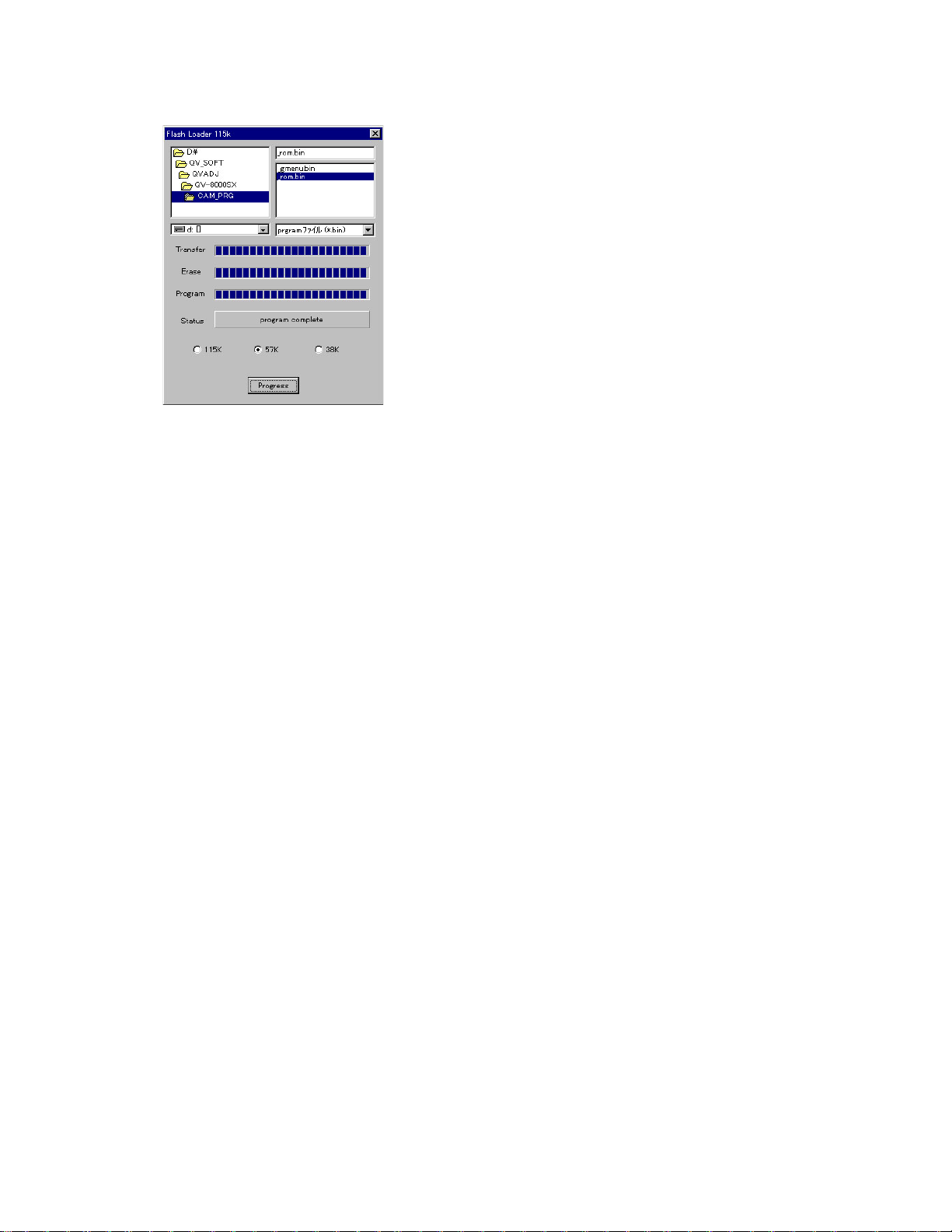
(8) Data transmission starts.
(9) Data transmission is completed normally when Status box shows "program complete."
(10) Disconnect AC adaptor plug (cannot be turned off by the power switch).
(11) Change the CompactFlash card with one for shooting.
(12) Boot the test mode and confirm the version.
Turn the camera on while pressing DISP and MENU buttons.
(13) Shoot a picture and confirm the camera function (shooting and playback.)
— 8 —
Page 11

2. Test mode
Note: Do not perform the menu item unless explained here. (It may damage the internal data and
camera becomes unusable.)
2-1. Booting
To boot the test mode;
Turn the camera on while pressing DISP and MENU buttons.
To boot MENU1
Press FLASH ➜ FLASH ➜ MENU keys in order rapidly.
To boot MENU2
Press SELF ➜ SELF ➜ MENU keys in order rapidly.
* To execute
Use + or – keys to select a test item then press shutter button to execute it.
2-2. Item for testing
2 TEST MODE
TEST MODE
PROG 99.08.16.13.38
GMENU 99.07.12.15.04
LOADER 0X00000007
ADJ
MOTOR 0X0000011A
POWER 0X1A
CCD ADJ1 YES
CCD ADJ2 YES
STROBE ADJ YES
ZOOM ADJ YES
FOCUS ADJ YES
2 MENU1
MENU1
1. INIT.NTSC JAPANESE
2. INIT.NTSC ENGLISH
3. INIT.PAL ENGLISH
4. CROSS HATCH
5. BLACK
6. WHITE
7. GRAY SCALE(10STEP)
8. 50PERCENT GRAY
9. COLOR BAR
·
TEST MODE
·
PROGRAM Version
·
Graphic Menu Version
·
Loader Version
·
ADJ Version
·
Motor MCU Version
·
Power MCU Version
·
CCD ADJUST 1 (Yes/No/NG)
·
CCD ADJUST 2 (Yes/No/NG)
·
STROBE ADJUST (Yes/No/NG)
·
ZOOM ADJUST (Yes/No/NG)
·
FOCUS ADJUST (Yes/No/NG)
Shown in green if all the adjustments
have been done.
YES when adjustments are completed.
NO when adjustments are incomplete.
NG if adjustments are failed.
— 9 —
Page 12

3 MENU2
MENU2 1/3
1. CCD ADJUS1
2. CCD ADJUS2
3. STROBE ADJUST
4. DISPLAY LENS ADJ
5. SDRAM CHECK
6. KEY CHECK
7. LED CHECK
8. CF CHECK
9. BATT. TEST
10. REC INFO
MENU2 2/3
11. NOISE CAPTURE
12. BAYER CAPTURE
13. PROG+GMENU UPDATE
14. PROG UPDATE
15. GMENU UPDATE
16. CF WRITE TEST
17. AF DATA SAVE
18. OSD DATA CHECK
19. ERROR MESSAGE TEST
20. EEPROM TEST
MENU2 3/3
21. SHUTTER CLOSE REC
22. SHUTTER SPEED CONST
23. SUB LCD CHECK (713)
24. ANG DET CHECK (713)
25. CHECK SUM
26. IRDA SLAVE
27. IRDA FACTORY SLAVE
28. IRDA MASTER
29. ZOOM ADJ (KX713)
30. FOCUS ADJ (KX713)
— 10 —
Page 13
3. Product conditions
3-1. Color adjustment data writing
1. Summary
(1) QV-2000UX is a high quality digital camera and makeshift adjustments cannot cover the quality of the
camera's picture.
Therefore, we have prepared set of lens ass'y that is adjusted precisely in the factory and a floppy disc
containing the lens'es adjustment data as spare parts.
(2) These adjustment data are stored in the EEPROM on PCB D.
2. Repairs
It is necessary to write color adjustment data for the replacements of the following units.
(1) Lens ass'y
(2) PCB D (when EEPROM contents can be read)
(3) PDB D and lens ass'y (when EEPROM contents cannot be read)
3. To replace the lens ass'y
(1) Connect AC adaptor and PC link cable to the camera.
Note: Connect the link cable to serial port COM1.
(2) Turn the camera on to set it on PLAY mode.
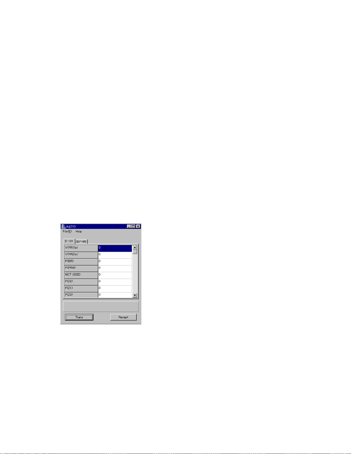
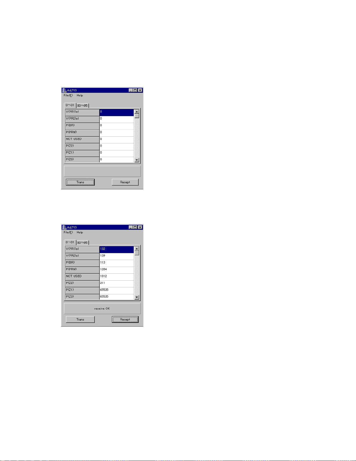
(3) Boot adjustment program ADJ713.EXE.
At this time, each adjustment data are 0.
— 11 —
Page 14
(4) Read the adjustment data of before repairs.
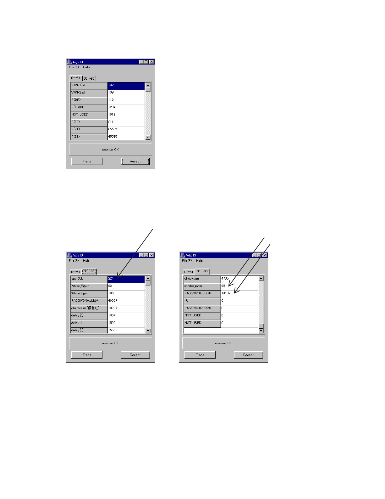
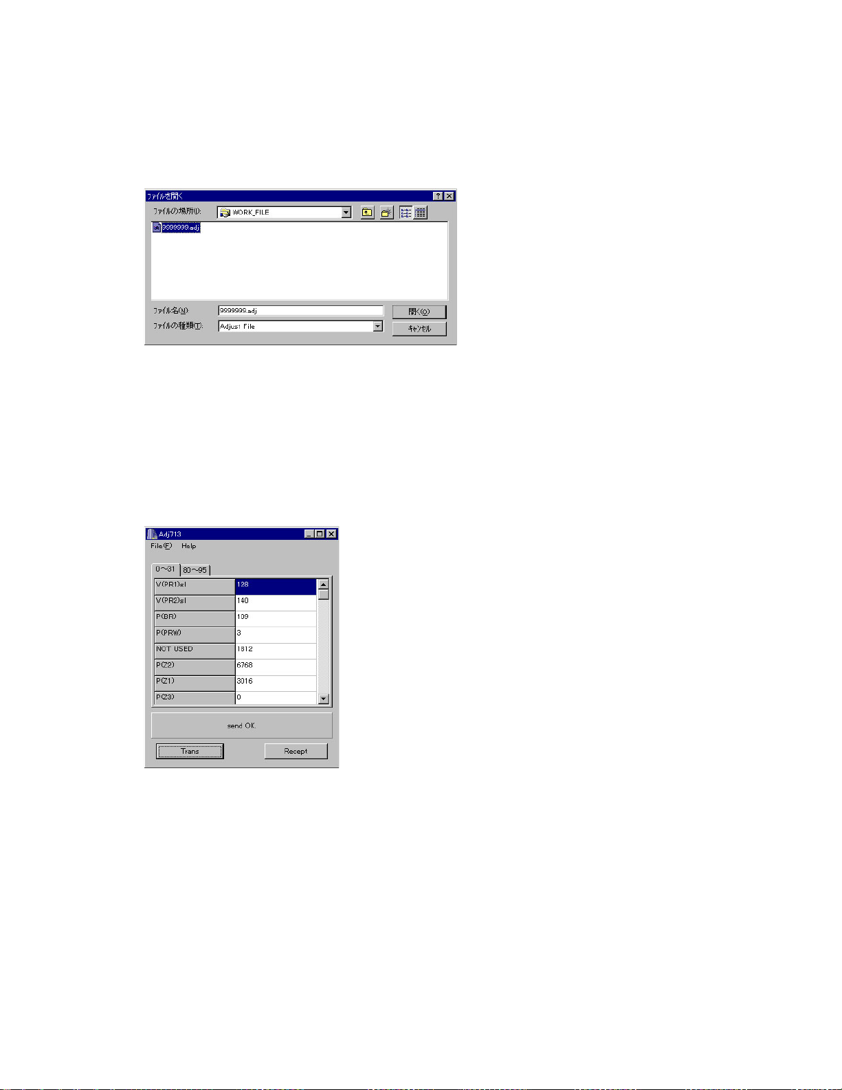
Click the Receipt button. “receive OK” will be indicated and adjustment data are shown.
Reference: At this time you can save the adjustment data in your PC.
File (F) ➜ Save as (A)
Select the drive and name the file then save it.
(Note: Do not forget to put extension code ".ADJ".)
(5) Write down the following numbers.
agc-6ab
strobe-pwm
P ASSWD (D x3333)
(6) Replace the lens ass'y.
(Adjusted in the factory and comes with adjustment data)
(7) Connect AC adaptor and PC link cable to the camera.
(8) Turn the camera on and set it on PLAY mode.
(9) Boot the adjustment program (ADJ713.EXE).
— 12 —
Page 15

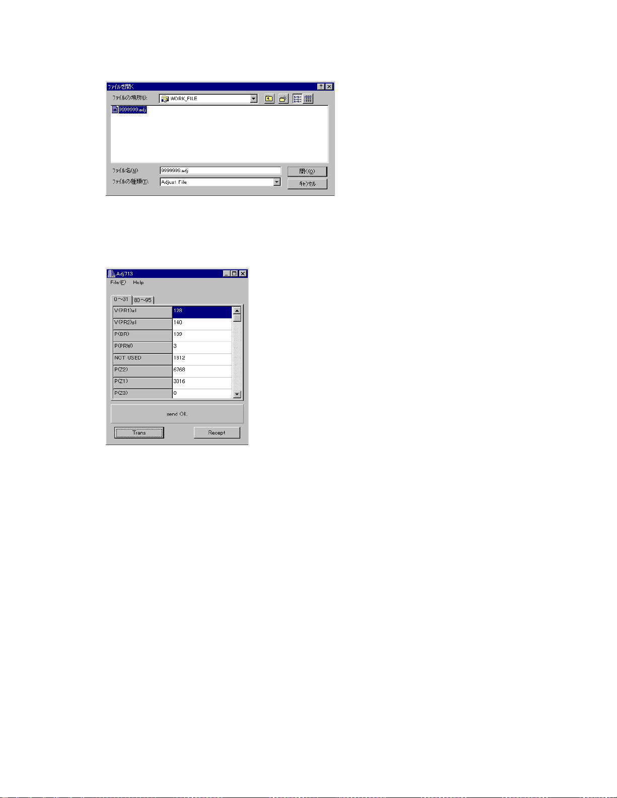
(10) Insert the floppy disc containing adjustment data of the lens ass'y in your PC and read the data.
File (F) ➜ Open (O)
Select FDD
Select adjustment data file with extension code .ADJ.
* Adjustment data file name: 9999999.ADJ
* 9999999 is the 7-digit number written on the seal stuck on the side of the lens unit.
(11) Change the following data with the number you have written on step 5 (data before replacing the lens
unit).
Caution: Never change the other data.
Agc-6db
Strobe-pwm
PASSWD (D x 3333)
(12) Transfer the data to the camera.
Click Trans button on ADJ window.
“send OK” will be shown.
(13) Turn the camera off.
(14) Check the camera operation by shooting a picture and play it back.
— 13 —
Page 16
4. To replace PCB D (in case the contents of EEPROM can be read)
(1) Connect AC adaptor and PC link cable to the camera.
Note: Connect the link cable to serial port COM1.
(2) Turn the camera on to set it on PLAY mode.
(3) Boot adjustment program ADJ713.EXE.
At this time, each adjustment data are 0.
(4) Read the adjustment data of before repairs.
Click the Receipt button. "receive OK" will be indicated and adjustment data are shown.
(5) Save the adjustment data in the PC.
File (F) ➜ Save as (A)
Select a drive to save data.
Name a file name then save the data.
(It is better to name the camera's serial number as the file name.)
XXXXXXXX.ADJ (Note: do not forget the extension code .ADJ.)
(6) Replace the PCB D
(7) Connect AC adaptor and PC link cable to the camera.
(8) Turn the camera on and set it on PLAY mode.
(9) Boot the adjustment program (ADJ713.EXE).
— 14 —
Page 17
(10) Load the saved data of the lens unit.
(11) Transfer the data to the camera.
Click Trans button on ADJ window.
“send OK” will be shown.
(12) Turn the camera off.
(13) Check the camera operation by shooting a picture and play it back.
— 15 —
Page 18
5. In case of replacing PCB D and lens ass'y (EEPROM on PCB D contents cannot be read)
(1) Replace PCB D and lens ass'y.
(2) Connect AC adaptor and PC link cable to the camera.
Note: Connect the link cable to serial port COM1.
(3) Turn the camera on to set it on PLAY mode.
(4) Boot adjustment program ADJ713.EXE.
(5) Insert the floppy disc containing adjustment data of the lens ass'y in your PC and read the data.
File (F) ➜ Open (O)
Select FDD
Select adjustment data file with extension code .ADJ.and load it.
(6) Transfer the adjustment data to the camera.
Clock Trans button on ADJ program window.
Send OK. Will be shown.
(7) Turn the camera off.
(8) Shoot a picture and play it back to check the camera function.
— 16 —
Page 19

3-2. Flash adjustment
1. General
Do not fail to perform this adjustment when you replace the flash unit.
2. Necessary equipment
(1) Dark room
(2) AC adaptor
(3) Gray paper (Superior's oxford gray No. 22)
The following sizes are available from us (also available from camra shop).
Parts code Parts name Specifications
1904 5411 Superior photographing background paper No. 22 (1.75 x 2.7m)
1904 5412 Sperior photographing background paper No. 22 (2.72 x 11m)
3. Condition
(1) Perform in a dark room.
(1) Distance between flash lens and gray paper should be 1 meter.
(1) Use lighter color of the gray paper.
Paper should be larger enough to fit in a picture taken from 1 meter distance.
(Reference; more than 1.5m x 2.0m)
4. Adjustment
(1) Connect an AC adaptor to the camera.
(2) Set the camera in REC mode.
(3) Boot the MENU2 in the test mode.
Turn the camera on while pressing DISP and MENU keys sumultaneously.
Press SELF ➜ SELF ➜ MENU in order quickly.
(4) Using + and – keys, choose STROB ADJUST and press the shutter button.
(5) When STROBE indicator appears on the right upper corner, turn the light off then press the shutter with
the above conditions.
(6) The camera flashes more than 4 times.
(7) Confirm the following indication and turn the camera off.
EEP WR OK
PWM XX
XXX
(8) Boot the test mode.
Turn the camera on while pressing DISP and MENU keys.
(9) Make sure that STROB ADJ column is YES.
(10) Turn the camera off.
5. Block diagram
Back ground paper.
1m
MENU
SET
MF/ /
/
ACCESS
MODE
T
CARD
W
PLAY
ON/OFF
DISP
— 17 —
Page 20

3-3. Flash operation and recharge operation
•Set QV-2000UX in “REC” mode.
•Normal Recording mode.
•Apply 6.0 ± 0.1 V voltage on DC in jack.
1. Preparation
(1) AC adaptor or stabilizer.
(2) Digital oscilloscope.
(3) Ammeter.
(4) TV (With video terminal).
(5) Video cable.
2. Adjustment and checking
(1) Shoot a picture with flash OFF. (Make sure there is no flash)
(2) Shoot a picture with flash ON and make sure it flashes once.
(3) Shoot in red eye reduction mode and make sure it flashes twice.
(4) Connect QV-7000SX and TV with video cable and make sure that the pictures taken in steps (2) and (3)
are not whitish, dark or erroneously colored.
(5) Make sure that the charging current is less than 1.3 A.
(6) Monitor the waveform of (1), (2) and (3) on a digital oscilloscope when flash goes on, and make sure
there are no errors comparing with the waveforms shown on the next page.
3. Notes
(1) Excuete in a dark room.
(2) Shoot a colorful object as much as possible.
Digital oscilloscope
TIME : 1.0 µsec/DIV
VOLTS : 1 V/DIV (AC mod)
Flash lens face
Probe close to
flash lens face
QV-2000UX
TV
(With video terminal)
Video cable
— 18 —
Page 21

Flash trigger waveform
1. Normal waveform TIME : 1 µ sec/DIV
VOLTS : 1 V/DIV
CH1
1V
vX⁄Pg
}CiX⁄ Pg
ACQUIRE
NORMAL
2. NG waveforms when trigger skipping occurs.
ENVELOPE
1
757µV
vX⁄ Qg¯g
g‘“o˜¢Œ˛OKB
2
AVS
REPET
ON | OFF
SAVE ON
ON | OFF
UERT1µV
(1) When trigger skipping occurs on the first
positive pulse.
(2) When trigger skipping occurs on the first
negative pulse.
— 19 —
Page 22

3-4. Current consumption
•Set QV-2000UX to “PLAY” mode.
1. Preparation
(1) Voltage regulator.
(2) Ammeter.
2. Adjustment procedure
(1) Current consumption (DC in = 6.0 ± 0.1 [V])
• Make sure that current consumption is less than 550 mA in PLAY mode.
• Make sure that current consumption is less than 800 mA in REC mode.
(Flash charge current is not included)
(2) Lower the voltage from 6 V as shown below then make sure the battery warning indicator changes.
DC in = 5.0 ± 0.05 [V] (one indicator is off )
DC in = 4.65 ± 0.05 [V] (two indicators are off)
DC in = 4.35 ± 0.06 [V] (All the indicators are off)
— 20 —
Page 23

3-5. VCOM DC adjustment
1. Preparation
(1) AC adaptor or stabilizer.
(2) Photo sensor/ Photo sensor amp (C2719)/L.P.F
(3) Digital oscilloscope.
2. Adjustment and checking
(1) Turn the power on while pressing DISP and MENU keys simultaneously. (TEST MODE)
(2) Push FLASH ➜ FLASH ➜ MENU keys in order rapidly. (TEST MODE 1)
(3) Choose 50 PERCENT GRAY and execute it.
(4) Monitor the photo sensor amplifier output via a low-pass filter of cutoff frequency 60Hz.
Monitoring the oscilloscope screen, adjust VR321 to minimize 60Hz ripple waveform.
3. Notes
Perform these adjustments when you replace LCD module or PCB L.
Photo diode
S1153
MENU
SET
LCD
QV-2000SX
(Reference) Easy adjustment
(1) Shot a monoscope pattern with the camera and adjust VR321 so that the best 10-step gradation is
taken.
ON/OFF
L.P.F
Photo Sensor Amp
C2719
Oscilloscope
MF/ /
/
MODE
T
PLAY
DISP
W
ACCESS
CARD
Minimize the
ripple components
10-step gradation
10-step gradation
Monoscope pattern
— 21 —
Page 24

3-6. Operation check
1. Preparation
(1) Batteries.
(2) AC adaptor.
(3) PC (IBM compatible)/OS:Windows 95/98.
(4) Link cable.
(5) Photo loader (program).
(6) TV (with video teminal).
(7) Video cable.
(8) USB cable/USB driver
(9) Test chart (for photography check)
(That which carried out color printing of picture data "CHART1.JPG" and the "CHART2.JPG".)
2. Check matter
(1) Photography check (Please be sure to carry out.)
1 Shoot the test chart without flashing.
2 Shoot the test chart with flashing.
3 Confirm the result (compare with properly functioning camera) for;
• Color
• Focus and resolution
(2) Unti-shock check, Battery operations, AC adaptor operations
(3) Switch operation.
(4) CompactFlash insertion/pulling out movement, cover open/close operations, flash up operation
(5) Optical zoom finder function
(6) Sub LCD display check
(7) Resolution, color reproduction check
(8) AE function, AF function, zoom operation
(9) IrDA transmission check (model C for export only)
(10) Video output, serial (3-pin) data transmission, USB function check
(11) Dust and scratches on lens.
(12) Appearance check
3. Note
(1) Make sure Video out setting are appropriate to your country.
(i.e. Japan=NTSC, England = PAL)
4. Test chart picture
— 22 —
CHART2.JPGCHART1.JPG
Page 25

4. D-PCB Assy
4-1. VCO free run frequency adjustment
1. Adjustment procedure
• Make sure
VCC2 (CP344) = 5.0 ± 0.05 [V]
VCC13 (CP361) = 12.75 ± 0.05 [V]
VCC7 (CP390) = 7.5 ± 0.05 [V]
VEE2 (CP391) = -14.25 ± 0.05 [V]
• Room temperature should be 20 ± 10 ºC
2. Preparation
• AC adaptor or voltage regulator
• Frequency counter
3. Adjustment and checking
(1) Connect SYF (CP355) and GND (CP350).
(2) Monitor HDB (CP704) with frequency counter and adjust VR320 so that frequency becomes 15.734
± 0.1 KHz.
(3) After completing adjustment, disconnect SYF (CP7033) and GND (CP700).
4-2. VCOM AC adjustment and VCOM DC coarse adjustment
1. Adjustment procedure
• Make sure
VCC2 (CP344) = 5.0 ± 0.05 [V]
VCC13 (CP361) = 12.75 ± 0.05 [V]
VCC7 (CP390) = 7.5 ± 0.05 [V]
VEE2 (CP391) = -14.25 ± 0.05 [V]
2. Preparation
• AC adaptor or voltage regulator
• Frequency counter
3. Adjustment procedure
(1) Make sure amplitude of VCOM output (CP364) is 6.6 ± 0.3 V.
(2) Adjust VR321 so that maximum VCOM output (CP364) will be 4.8 ± 0.2 V.
4. Note
When unable to adjust using AC adaptor, use voltage regulator and supply power to be VCC1-1 (CP105)
= 5.0 ± 0.05 V.
— 23 —
Page 26

4-3. RGB AMP, Sub bright adjustment
1. Adjustment procedure
• Make sure
VCC2 (CP344) = 5.0 ± 0.05 [V]
VCC13 (CP361) = 12.75 ± 0.05 [V]
VCC7 (CP390) = 7.5 ± 0.05 [V]
VEE2 (CP391) = -14.25 ± 0.05 [V]
2. Preparation
• AC adaptor or voltage regulator
• Frequency counter
3. Adjustment and checking
(1) Turn the power on while pressing DISP and MENU keys simultaneously. (TEST MODE)
(2) Push FLASH ➜ FLASH ➜ MENU keys in order rapidly. (TEST MODE 1)
(3) Select GRAY SCALE (10STEP) and execute.
(4) Apply VCC2-1 (CP344) on the killer terminal (CP308) via 22k ohm resistor.
(5) Trigger VB waveform (CP322) by FRP (CP305) signal to adjust as noted below.
(6) Adjust RGB-AMP VR (VR302) so that VG waveform (CP322)’s pedestal-pedestal voltage is 3.5+/-0.05
Vp-p.
(7) Adjust SUB R BRIGHT VR (VR305) so that VR waveform (CP320)’s pedestal-pedestal voltage is 3.5+/
-0.05 Vp-p.
(8) Adjust SUB B BRIGHT VR (VR304) so that VB waveform (CP324)’s pedestal-pedestal voltage is 3.5+/
-0.05 Vp-p.
* Make sure that waveforms are not distorted.
* Proceed to CONTRAST, BRIGHT adjustments.
Power
Supply
VCC13
VCC2
VCC7
VEE2
QV-2000UX
D-PCB
(CP361)
(CP344)
(CP390)
(CP391)
Killer terminal
(CP308)
VR(CP320)
VG(CP322)
VB(CP324)
VCC2-1
22KΩ
Digital oscilloscope
Figure 3-1
3.5 ± 0.05 V
(pedestal-pedestal)
— 24 —
3-1
Page 27

4-4. Contrast, Bright adjustments
1. Adjustment procedure
• Make sure
VCC2 (CP344) = 5.0 ± 0.05 [V]
VCC13 (CP361) = 12.75 ± 0.05 [V]
VCC7 (CP390) = 7.5 ± 0.05 [V]
VEE2 (CP391) = -14.25 ± 0.05 [V]
• RGB AMP and SUB BRIGHT adjustments should be completed (proceed from those adjustments.)
2. Preparation
• AC adaptor or voltage regulator
• Frequency counter
3. Adjustment and checking
(1) Turn the power on while pressing DISP and MENU keys simultaneously. (TEST MODE)
(2) Push FLASH ➜ FLASH ➜ MENU keys in order rapidly. (TEST MODE 1)
(3) Select GRAY SCALE (10STEP) and execute.
(4) Apply VCC2-1 (CP344) on the killer terminal (CP308) via 22k ohm resistor.
(5) Trigger VB waveform (CP322) by FRP (CP305) signal to adjust as noted below.
(6) Adjust contrast VR (VR306) so that contrast terminal voltage (CP306) is 1.50 ± 0.05 V temporary.
(7) Adjust Bright VR (VR303) so that pedestal-4th step is 2.10+/-0.05Vp-p.
(8) Adjust Contrast VR (VR306) so that pedestal-10th step (white 100 %) is 2.85+/-0.05Vp-p.
(9) After the adjustment, remove the 22k ohm resistor between killer terminal (CP308) and VCC2 (CP344).
* Make sure that waveforms are not distorted.
Power
Supply
VCC13
VCC2
VCC7
VEE2
QV-2000UX
D-PCB
(CP361)
(CP344)
(CP390)
(CP391)
Killer terminal
(CP308)
VG(CP322)
VCC2-1
22KΩ
Digital oscilloscope
Figure 3-2
2.85 ± 0.05 V
(pedestal-10 step)
— 25 —
3-2
Page 28

4-5. Color adjustment
1. Adjustment procedure
• Make sure
VCC2 (CP344) = 5.0 ± 0.05 [V]
VCC13 (CP361) = 12.75 ± 0.05 [V]
VCC7 (CP390) = 7.5 ± 0.05 [V]
VEE2 (CP391) = -14.25 ± 0.05 [V]
• Perform this adjustment after Contrast adjustment.
2. Preparation
• AC adaptor or voltage regulator
• Frequency counter
3. Adjustment and checking
(1) Turn the power on while pressing DISP and MENU keys simultaneously. (TEST MODE)
(2) Push FLASH ➜ FLASH ➜ MENU keys in order rapidly. (TEST MODE 1)
(3) Select and execute COLOR BAR.
(4) Trigger with FRP (CP305) signal.
(5) Adjust VR300 so that pulse width of 4th VB waveform (CP324) (pedestal-peak) is 2.85+/-0.05Vp-p.
(6) Proceed to TINT adjustment.
4. Note
Perform the adjustment after (continuously from) Color adjustment.
QV-2000UX
D-PCB
(CP361)
(CP344)
(CP390)
(CP391)
Power
Supply
VCC13
VCC2
VCC7
VEE2
VB(CP324)
Digital oscilloscope
1432
2.85 ± 0.05 [Vp-p]
— 26 —
Page 29

4-6. TINT adjustment
1. Adjustment procedure
• Make sure
VCC2 (CP344) = 5.0 ± 0.05 [V]
VCC13 (CP361) = 12.75 ± 0.05 [V]
VCC7 (CP390) = 7.5 ± 0.05 [V]
VEE2 (CP391) = -14.25 ± 0.05 [V]
• Perform this adjustment after Contrast adjustment.
2. Preparation
• AC adaptor or voltage regulator
• Frequency counter
3. Adjustment and checking
(1) Turn the power on while pressing DISP and MENU keys simultaneously. (TEST MODE)
(2) Push FLASH ➜ FLASH ➜ MENU keys in order rapidly. (TEST MODE 1)
(3) Select and execute COLOR BAR.
(4) Trigger with FRP (CP305) signal.
(5) Adjust VR301 so that potential difference between the 2nd and 4th pulses' height (pedestal-peak) (A
and B) of VB waveform (CP324) is less than 0.1Vp-p.
4. Note
Perform the adjustment after (continuously from) Color adjustment.
QV-2000UX
VCC13
VCC2
D-PCB
(CP361)
(CP344)
Power
Supply
VCC7
VEE2
(CP390)
(CP391)
VB(CP324)
Digital oscilloscope
1432
BA
— 27 —
Page 30

5. PW-PCB Assy
5-1. VCC3, VCC3-1, VCC5, VCC5-1 Voltage check
1. Preparation
•AC adaptor or voltage regulator
•Multimeter
2. Adjustment procedure
Make sure
VCC3 (CP112) = 3.3 ± 0.1 [V]
VCC3-1 (CP113) = 3.3 ± 0.1 [V]
VCC5 (CP115) = 5.0 ± 0.15 [V]
VCC5-1 (CP116) = 5.0 ± 0.15 [V]
3. Note
When unable to adjust using AC adaptor, use voltage regulator and supply power to be VCC-1-3 (CP108) =
5.0 ± 0.05 V.
5-2. VCC15, VEE7 Voltage check
1. Preparation
•AC adaptor or voltage regulator
•Multimeter
2. Adjustment procedure
•Adjust VR100 so that VCC15 (CP118) is 15.0 ± 0.1 V.
•Adjust VR101 so that VEE7 (CP117) is –7.5 ± 0.1V.
3. Notes
When unable to adjust using AC adaptor, use voltage regulator and supply power to be VCC-1-3 (CP108) =
5.0 ± 0.05 V.
— 28 —
Page 31

5-3. VCC2 adjustment and VCC13, VCC7, VEE2 Voltage check
1. Preparation
•AC adaptor or voltage regulator
•Multimeter
2. Adjustment procedure
Adjust VR951 so that VCC2 (CP972) = 5.0 ± 0.02 V.
Make sure
VCC13 (CP970) = 11.4 ~ 14.1 [V]
VCC7 (CP971) = 6.8 ~ 8.6 [V]
VEE2 (CP972) = –11.0 ~ –16.5 [V]
3. Notes
When unable to adjust using AC adaptor, use voltage regulator and supply power to be VCC-1-L (CP107) =
5.0 ± 0.05 V.
5-4. BL drive voltage adjustment
1. Preparation
•AC adaptor or voltage regulator
•Multimeter
2. Adjustment procedure
Make sure that BL-VCC (CP910) is within 5.4 ± 0.2V.
3. Notes
When unable to adjust using AC adaptor, use voltage regulator and supply power to be VCC-1-L (CP107) =
5.0 ± 0.05 V.
— 29 —
Page 32

6. SUB-PCB Assy
6-1. Clock oscillation check
•Turn power off
•Room temperature should be 25 ± 10 °C.
1. Preparation
Pedometer or frequency counter or quartz timer.
2. Adjustment procedure
Execute one of check from the followings.
(1) Pedometer: within 62 ppm.
(2) Frequency counter check point CP401 signal pad; 32.768 ± 0.002 [KHz].
(3) After setting time turn power off. 30 minutes later check the time.
— 30 —
Page 33

DISASSEMBLY
Due to changes of parts to use, the disassembly procedure described below is subject to change.
*
1. Remove 1 screw (S2) from the bottom of tha
camera.
4. Remove 1 screw (S2) on the other side of the
camera.
screw (S2)
2. Open the battery cover and remove 1 screw (S8).
screw (S8)
3. Remove 2 screws (S1) from side body of the
camera.
screw (S2)
5. Open CN cover and remove 1 screw (S1).
screw (S1)
6. Insert (–) precision screwdriver to the side of the
flash unit.
screw (S1)
7. Unhook the top case as you push it upward, and
open it.
hook
— 31 —
Page 34

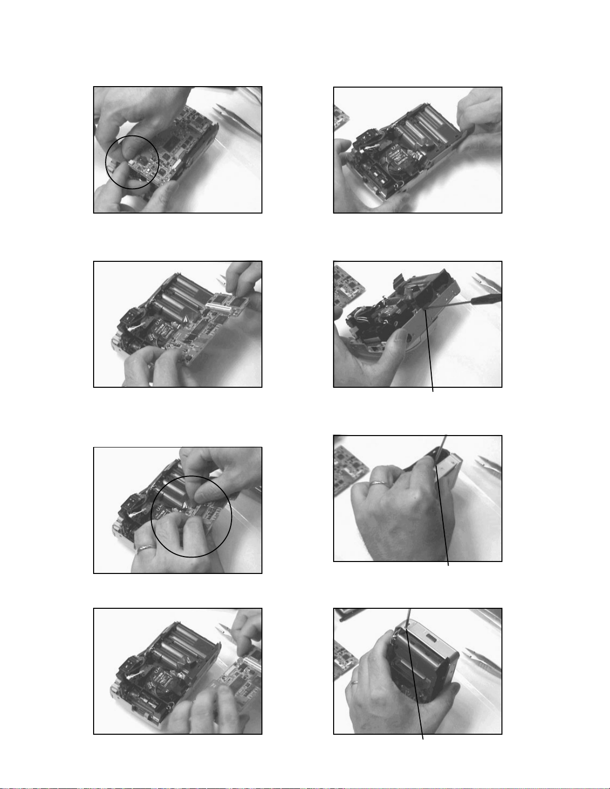
8. Open the top case.
9. Disconect the flat cable.
12. Desolder the cable.
Signal wire
Shield
10. Remobe the top case.
11. Desolder the wire.
13. Remove 4 screws (S5) affixing DP frame.
screws (S5)
— 32 —
Page 35

screws (S5)
16. Display unit separated.
17. Dsconnect 3 flat cables.
(Make sure not to cut them.)
14. Lift up DP frame and remove the connector on BL
PCB.
15. Disconnect a flat cable on LCD.
— 33 —
Page 36
18. Remobe a connector that links to the finder.
22. Remove the battery cover.
19. Open D PCB.
20. Disconnect the flat cable that links to Lens ass’y.
(Make sure not to cut it.)
23. Remove 1 screw (S2) on BT frame.
screw (S2)
24. Remove 1 screw (S8).
21. Remove D PCB.
screw (S8)
25. Remove 1 screw (S2) from side body of the
camera.
screw (S2)
— 34 —
Page 37

26. Open CF cover and remove 2 screws (S3).
29. Remove 1 screw (S4).
screws (S3)
27. Unhook (two parts) BT frame.
screw (S4)
30. Remove 1 screw (S4).
screw (S4)
31. Remove 2 battery springs.
28. Take care not to damage battery springs and
remobe BT frame.
— 35 —
Page 38

32. Remove the lens frame by pulling it out from the
bottom.
35. Remove a connector on SUB unit.
36. Remove 3 screws (S4).
33. Take out CF card if it is loaded.
34. Remove SUB unit.
screws (S4)
— 36 —
Page 39

37. Open PW PCB.
38. Connect resistor (1.5 kW / 5 w) to flash capacitor
for discharging.
40. Remove 2 screws (S4).
screws (S4)
@
39. Remove a connector and then remove PW
PCB.
41. Remove 2 screws on the flash unit.
screw (S4)
— 37 —
Page 40

screw (S4)
44. Remove FT gear shaft supporter, FT gear, and
FT gear shaft in order.
42. Remove flash unit (flash is opened at this point).
open
45. Remove 4 screws (S8) affixing Lens PCB.
screws (S8)
43. Remove 1 screw (S2).
screw (S2)
— 38 —
Page 41

46. Remove Lens PCB.
48. Remove the finder.
screw (S8)
Cautions in assembly procedures
1. When you assemble the finder, first turn the cam all
the way to wide angle.
47. Remove 2 screws (S8) affixing the finder.
screws (S6)
@
2. When assembling No.26 GEAR/FT, a square mark
is turned upward.
3. When assembling FKEY PCB with 4 screws (S2), do
not screw forcibly.
(Doing so may cause the malfunction of cursor keys.)
screw (S2)
— 39 —
Page 42

S5
EXPLODED VIEW
X4
63
E1
31
12
S2
32-1
18
10
S2
19
X2
8
11
S1
X2
9
20
23
14
S1
17
16
S2
27
15
S2
25
26
34-3
S8
S2
X2
X2
13
24
S8
X2
28
34-2
4
3-2
S2
3-3
3-4
3-1
1-1
6
21
22
5
S4
3-4
3
3-3
2
1
S11
7
61
S4
56
S8
X2
X2
S4
57
59
S8
S2
39
40
S8
38
X2
42
X3
S9
S4
S2
44
43
58
S10
41
S2
30
S4
37
45
S2
X2
60
36
46
S4
S6
S10
47
48
29
S2
S4
S6
49
S4
S3
S2
52
55
50
62
51
53
54
S4
32
X2
33
S4
34
S7
34-1
35
— 40 —
Page 43

MAIN BODY COMPONENT
N Item Code No. Parts Name Specification Applicable Q
Price Code
N 1 6614 4094 BL ASSY K341725*1 Common 1 CE X
1-1 3851 2113 FLUORESCENT LAMP
CAS-1.8JS1.8-1
Common 1 AW A
N 2 6614 4540 SPACER/BACK LIGHT K441763-1 Common 1 AA X
N 3 1001 4044 LCD ASSY
K341919*1 TK(K7
Common 1 DJ -
3-1 2725 1347 LCD
COD18T1022RN
Common 1 DI B
N 3-2 6614 4220 PANEL/DISPLAY K441760-1 Common 1 AH B
N 3-3 6614 4230 TAPE/DOUBLE SIDE K441774-2 Common 2 AA B
N 3-4 6614 4240 TAPE/DOUBLE SIDE K441774-3 Common 2 AA B
N 4 6614 4530 FRAME/DISPAY K241200-1 Common 1 AC X
N 5 6614 4095 PCB ASSY/BACK LIGHT K441861*1 Common 1 BJ A
N 6 1000 5398 PLATE/SEALED K442017-1 Common 1 AA X
N 7 1000 5396 PLATE/INSULATION K441867-2 Common 1 AA X
N
8
6614 4980 CASE/UPPER K140616-1 QV-2000UX 1 AX X
N 1000 4448 CASE/UPPER K140616-2 QV-2000UX/Ir 1 AX X
N 9 6614 5010 BUTTON/MODE K341609-1 Common 1 AI X
10 6613 1330 PIN/STRAP R340181-2 Common 1 AE X
N 11 6614 5000 RUBBER KEY K341614-1 Common 1 AA X
N 12 6614 5020 BUTTON/POWER K341610-1 Common 1 AF X
N 13 6614 4070 PCB ASSY/KEY K341636*1 Common 1 BK A
N 14 6614 5040 BUTTON/SET K341607-1 Common 1 AE X
N 15 6614 5050 BUTTON/CURSOR K341608-1 Common 1 AE X
N 16 6614 5030 BUTTON/MENU K341606-1 Common 1 AE X
N 17 6614 5150 COVER/CONNECTOR K241206-1 Common 1 AE B
N 18 6614 5160 CASE/FD K341616-1 Common 1 AG C
N 19 6614 4990 KNOB/ZOOM K341620-1 Common 1 AA X
N 20 6614 4069 BATTERY COVER ASSY K341635*1 Common 1 AU A
21 1001 4228 PCB ASSY/DIGITAL
K140647*1 M
Common 1 EG A
N 22 1000 5396 PLATE/INSULATION K441867-2 Common 1 AA X
N 23 6614 4170 FRAME/BATTERY K140621-1 Common 1 AF X
N 24 1015 1535 FINDER LF-036Z Common 1 CN C
N 25 6614 4210 GEAR SHAFT SUPPORTER/FT K441753-1 Common 1 AB X
N 26 6614 4200 GEAR/FT K341634-1 Common 1 AA X
N 27 6614 4190 GEAR SHAFT/FT K441754-1 Common 1 AF X
N 28 6614 4150 SPRING/BATTERY K441756-1 Common 1 AC X
N 29 6614 4130 FRAME/LENS K140618-1 Common 1 AM X
N 30 6614 4180 LABEL/BATTERY K441896-1 Common 1 AA X
N 31 6614 4650 CF COVER ASSY K241260*1 Common 1 AZ B
N
32
1001 4230 SUB ASSY K341739*1 QV-2000UX 1 CS A
N 1001 4229 SUB ASSY K341739*2 QV-2000UX/Ir 1 DD A
N 32-1 2725 1391 LCD CA487-TS Common 1 AL X
N
32-2
6614 4091 PCB ASSY/SUB K441862*1 QV-2000UX 1 CK X
N 6614 4092 PCB ASSY/SUB K441891*1 QV-2000UX/Ir 1 DA X
N 33 6614 5210 PCB ASSY/BB K441743-1 Common 1 AR X
N 34 6614 4086 POWER ASSY K341741*1 Common 1 DI A
N 34-1 1015 1467 EJECTOR UNIT/CF 55370-0011 Common 1 AY X
N 34-2 6614 4140 SPRING/BATTERY K441755-1 Common 1 AB X
N 34-3 6614 4160 SPRING/BATTERY K441757-1 Common 1 AB X
N 35 6614 4088 LENS COVER ASSY K341704*1 Common 1 CA A
N
36
6614 4260 CASE/LOWER K140617-1 QV-2000UX 1 AW X
N 1000 5133 CASE/LOWER K140617-2 QV-2000UX/Ir 1 AY X
Notes: Q : Quantity used per unit
R : Rank
R
- 41 -
Page 44

N Item Code No. Parts Name Specification Applicable Q
Price Code
N 37 6614 4380 Lens cover supporter K341661-1 Common 1 AE X
N
38
6614 4910 PLATE/RATING K441889-1 QV-2000UX 1 AA X
N 6614 4920 PLATE/RATING K441889-2 QV-2000UX/Ir 1 AA X
N 39 6614 4400 COVER/LED K341656-1 Common 1 AA X
40 6613 1210 SCREW/STAND K341059-1 Common 1 AC X
N 41 6614 4440 SPRING/GUIDE K441797-1 Common 1 AA X
N 42 6614 4340 SPRING/GUIDE FOR FLASH K441793-1 Common 1 AA X
N 43 6614 4320 METAL/LOCK FOR FLASH K341650-1 Common 1 AD X
N 44 6614 4330 SPRING/GUIDE FOR FLASH K441792-1 Common 1 AA X
N 45 6614 4310 METAL/LOCK FOR FLASH K341649-1 Common 1 AB X
N 46 6614 4097 PCB ASSY/S
K241253*2 M
Common 1 AW A
N 47 6614 4300 FRAME/FD K341621-1 Common 1 AC X
N 48 6614 4290 COVER/FD K341605-1 Common 1 AI X
N 49 1015 1536 SENSOR UNIT/FLASH CO-713SU Common 1 AT X
N 50 3122 3754 BUZZER
PKM35-4A38
Common 1 AL X
N
51
6614 4270 COVER/IR K341613-1 QV-2000UX 1 AN X
N 6614 4280 COVER/IR K341613-2 QV-2000UX/Ir 1 AD X
N 52 6614 4370 PANEL/DISPLAY K441761-1 Common 1 AC X
N 53 6614 4350 BUTTON/SHUTTER K341611-1 Common 1 AH X
N 54 6614 4360 SPRING/SHUTTER K441762-1 Common 1 AA X
N 55 6614 4410 COVER/LED K341643-1 Common 1 AA X
N 56 1015 1503 FLASH UNIT CO-713 Common 1 BX A
N 57 6614 4390 SPRING/FLASH K441791-1 Common 1 AA X
N 58 5861 4367 Steel ball SUS304 3 Common 1 AA X
N 59 6614 4470 HARNESS/FLASH K441778-1 Common 1 AA X
N 60 6614 5140 HARNESS/SWITCH K441777-1 Common 1 AB X
N 61 6614 4900 RING/CAMERA K441752-1 Common 1 AK X
N 62 6614 4420 TAPE/DOUBLE SIDE K441774-4 Common 1 AA X
N 63 1001 4045 LENS UNIT S
K341898*1
Common 1 EH X
E1 5861 3649 E-RING 1.5 JISB2805 Common 1 AA X
N S1 5112 0825 SCREW BT3 1.7X3.5 BK Common 3 AA X
N S2 5861 3530 SCREW BT3 1.7X3.5 NI Common 17 AA X
S3 5112 0884 SCREW PS3 1.7X3 NI Common 2 AA X
S4 5860 1477 SCREW PS3 1.7X3.5 BK Common 14 AA X
S5 5860 0091 SCREW PS3 1.7X4.5 BK Common 4 AA X
S6 5112 0736 SCREW M1.7X3.5(BK) Common 3 AA X
S7 5861 3773 SCREW PS1 2X2.2 NI Common 1 AA X
N S8 9482 7200 SCREW BT3 1.4X4 NI Common 8 AA X
S9 6614 4450 SCREW K441807-1 Common 1 AA X
S10 6614 4460 SCREW K441808-1 Common 2 AA X
N S11 5861 3691 SCREW PS1 1.7X2.5 NI Common 2 AA X
ACCESSORY
Price Code
N 3851 2123 STRAP ST-K713 Common 1 AN X
1014 8773 CABLE/VIDEO VC-K723-FC Common 1 AR X
1015 1471 CABLE/PC-LINK
LC9F-DOS-K740-
QV-2000UX/Ir 1 BX X
1015 1538 CD-ROM
CK713DCA01R
QV-2000UX/Ir 1 AM X
N 1015 1539 CASE/SOFT SC-713 Common 1 BA X
2012 6146 CF CARD (8 MB)
SDCFB-8-200QV-
QV-2000UX/Ir 1 DH X
3502 2744 CABLE/USB 59204-2301 Common 1 BK X
3816 0266 LR6 alkaline batteries LR6PA/2ST QV-2000UX/Ir 2 AG X
Notes: Q : Quantity used per unit
R : Rank
R
N Item Code No. Parts Name Specification Applicable Q
- 42 -
R
Page 45

PRINTED CIRCUIT BOARDS
DIGITAL-PCB (PCB-713D-D)
— 43 —
Page 46

SUB-PCB (PCB-713D-SUB)
— 44 —
Page 47

POWER-PCB (PCB-713D-PW)
— 45 —
Page 48

BACK LIGHT-PCB (PCB-713D-BL)
KEY-A-PCB (PCB-713D-KA)
— 46 —
Page 49

KEY-B-PCB (PCB-713D-KB)
SWITCH-PCB (PCB-713D-SW)
— 47 —
Page 50

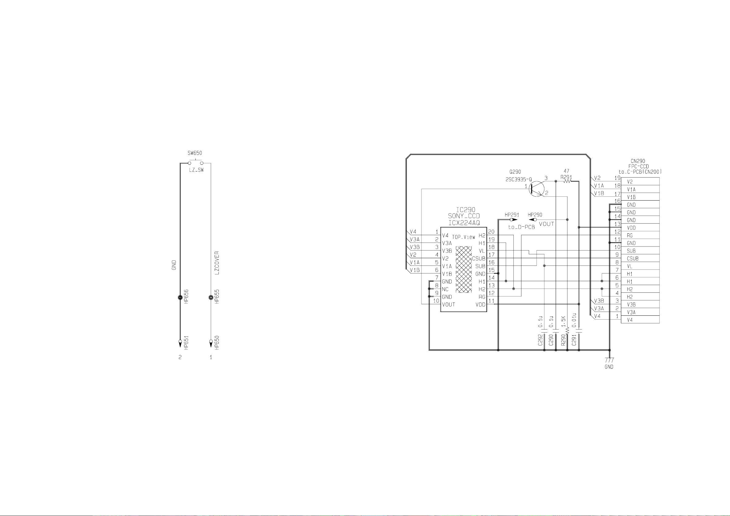
CCD-PCB (PCB-713D-FPC)
— 48 —
Page 51

DA-PCB (PCB-K713A-DA) CIRCUIT
SCHEMATIC DIAGRAMS
— 49 —
Page 52

DB-PCB (PCB-K713A-DB) CIRCUIT
— 50 —
Page 53
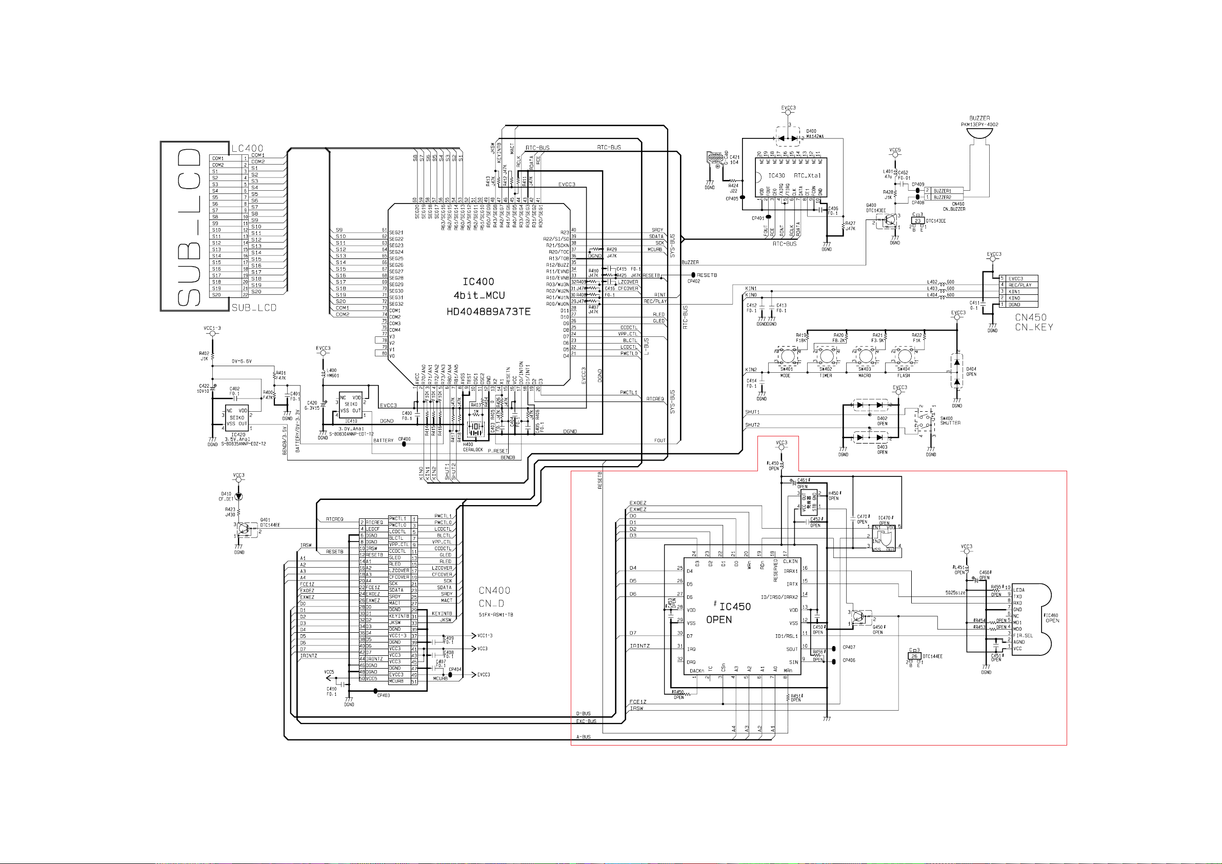
SUB-PCB (PCB-K713A-SUB) CIRCUIT
— 51 —
NOTE : Mounted only on the model QV-2000UX/Ir.
Page 54
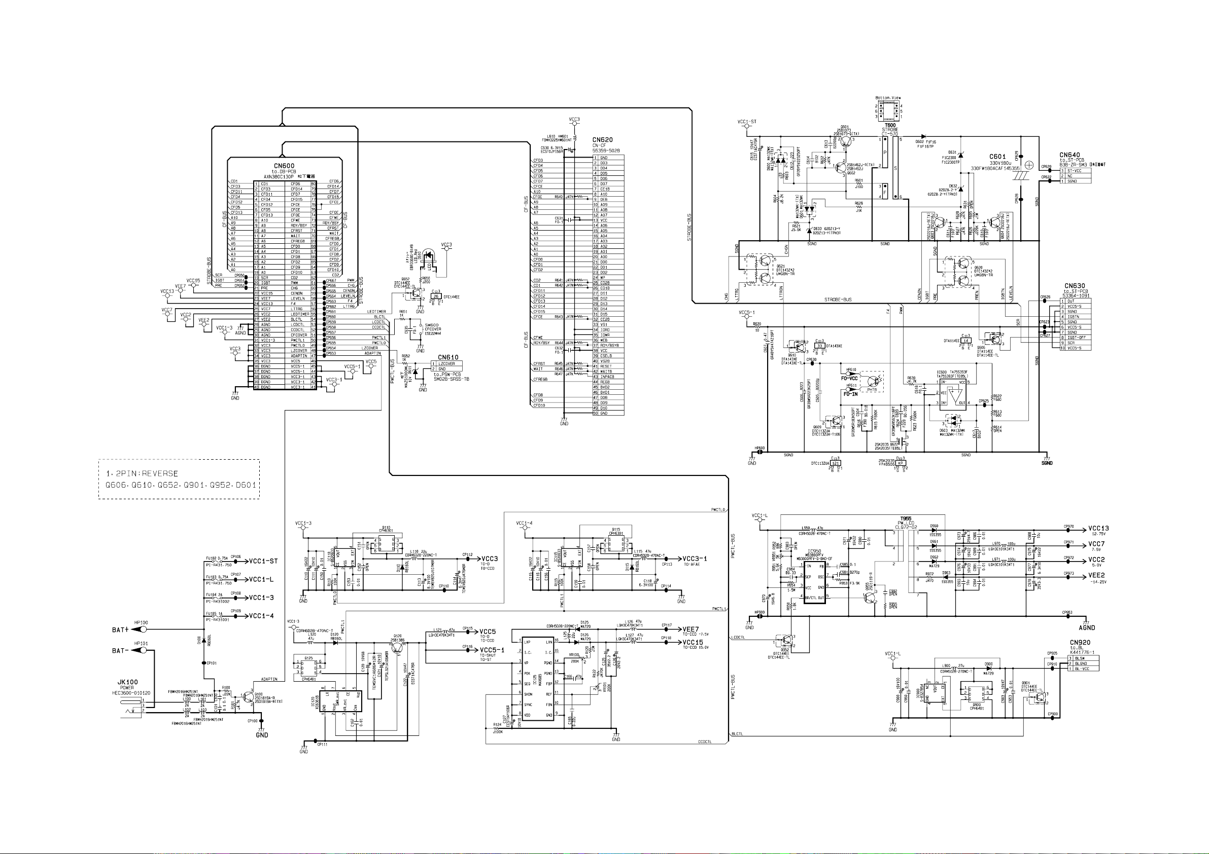
PW-PCB (PCB-K713A-PW) CIRCUIT
— 52 —
Page 55

BL-PCB (PCB-K713A-BL) CIRCUIT
— 53 —
Page 56

KA-PCB (PCB-K713A-KA) CIRCUIT KB-PCB (PCB-K713A-KB) CIRCUIT
— 54 —
Page 57
SW-PCB (PCB-K713A-SW) CIRCUIT FPC-PCB (PCB-K713A-FPC) CIRCUIT
— 55 —
Page 58

Ver.1 : The following items were changed.
• P.39 Cautions in assembly procedures
• P.40 EXPLODED VIEW
• P.41, 42 PARTS LIST
CASIO TECHNO CO.,LTD.
Overseas Service Division
Nishi-Shinjuku Kimuraya Bldg. 1F
5-25, Nishi-Shinjuku 7-Chome
Shinjuku-ku, Tokyo 160-0023, Japan
 Loading...