

Page 1

SERVICE MANUAL
(without price)
ELECTRONIC CASH REGISTER
QT-7300 (EX-963)
MAY. 2001
Page 2

CONTENTS
QT-7300 PAGE
1. EXPLANATION OF PRODUCT ................................................................... 1
1-1. General Description ................................................................................................... 1
1-2. System Overview........................................................................................................ 1
1-3. Major Component ....................................................................................................... 2
1-4. Specifications ............................................................................................................. 3
1-5. I/O Outlets ................................................................................................................... 5
2. DISASSEMBLY............................................................................................ 6
3. INSTALLATION ......................................................................................... 10
4. SYSTEM INSTALLATION.......................................................................... 11
4-1. CPU ............................................................................................................................ 11
4-2. DRAM......................................................................................................................... 11
4-3. HDD ............................................................................................................................ 12
4-4. Serial Ports................................................................................................................12
4-5. Parallel Port...............................................................................................................12
4-6. VGA ............................................................................................................................ 12
4-7. Ethernet ..................................................................................................................... 12
4-8. Cash Drawer.............................................................................................................. 13
4-9. Keyboard ................................................................................................................... 14
4-10. PS/2 Mouse ............................................................................................................... 14
4-11. External FDD ............................................................................................................. 14
4-12. Expansion Slot.......................................................................................................... 15
4-13. System O/S and Software Installation .................................................................... 15
4-14. Award BIOS Setup.................................................................................................... 16
4-15. Watchdog Function .................................................................................................. 28
4-16. Touch screen ............................................................................................................ 29
4-17. ETHERNET INTRODUCTION.................................................................................... 31
5. CIRCUIT EXPLANATIONS ........................................................................ 34
5-1. Explanations of each block ..................................................................................... 34
5-2. Block diagram........................................................................................................... 37
5-3. Jumper setting.......................................................................................................... 38
6. DIAGNOSTIC OPERATION....................................................................... 41
6-1. Diagnositc softwares ............................................................................................... 41
6-2. Customer display ..................................................................................................... 41
6-3. Drawer test ................................................................................................................ 45
6-4. Touch panel test ....................................................................................................... 46
7. TROUBLESHOOTING ............................................................................... 48
8. DATA SHEET............................................................................................. 50
8-1. Power Supply (100W) ............................................................................................... 50
9. CIRCUIT DIAGRAM ................................................................................... 51
10. PARTS LIST............................................................................................... 76
Page 3
1. EXPLANATION OF PRODUCT
1-1. General Description
The QT-7300 is a PC-based POS terminal which integrates SVGA, 12.1" LCD panel, Touch screen, Ethernet,
USB, multi I/O ports for wide range of PC peripherals and special PC technologies like watchdog timer together
with regular POS functionality like Cash Drawer interfaces all in a single system.
The QT-7300 features desktop free standing and wall mounting for a wide variety of applications. An unique cable
management device is also provided to trim the operation environment. In conformity to IPX1 standard, waterresistant system design is adopted. Designed by the PC and POS experts for the POS professionals, the QT7300 is virtually the ultimate solution for hospitality applications.
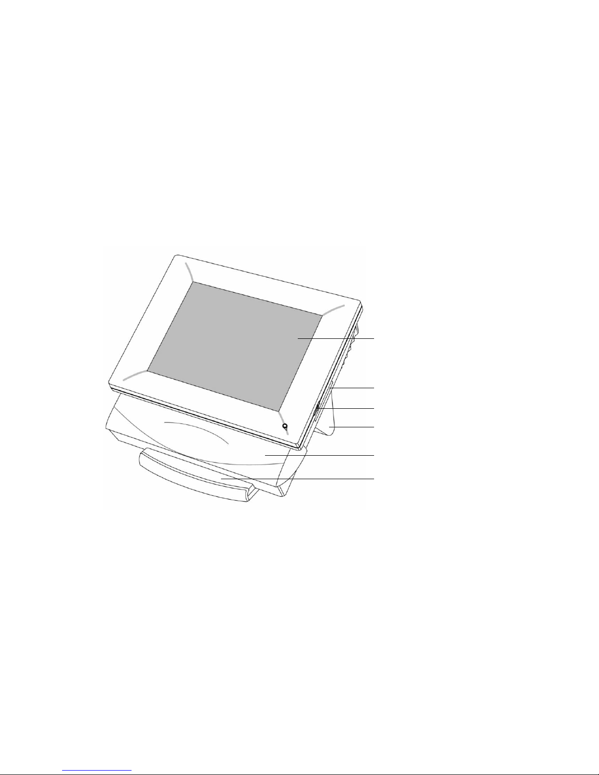
1-2. System Overview
Operator display with Touch screen
TFT color LCD
Side panel
LCD Display Contrast adjustment
Large Hinge cap (Large Hinge inside)
Cable management shroud
Main prop
— 1 —
Page 4

1-3. Major Component
1. Touchscreen: The QT7300 features a quick-response touchscreen for keyboardless operation. The
standard touch adapted in this computer is 12.1" analog resistive type Fujitsu touchscreen. Its durability is
10 million touches in life.
2. Flat panel: To provide the best visual resolution and viewing angle, the standard display panel adapted in
the QT7300 is 12.1" active-matrix TFT passive matrix flat panel.
3. Metal front compartment: The universal mounting design of the front metal compartment is able to mount
most brands of 12.1" flat panel and the EMI issue is also considered.
4. Touchscreen controller: The RS-232 touchscreen controller shares COM1.
5. Power supply: The power supply adapted in this computer is a super-slim 100W power which meets FCC/
VDE Class B specification.
6. System control board: The system engine used is SBC8360-4M. The controller combines both notebook
and industrial computer technology to most compact and stable computer.
7. Main prop: The main prop is made up by a inner metal piece with an outside plastic clothing. It consists of
a set of strong hinges to ensure the whole unit’s stability when a certain touch pressure is applied on the
touchscreen.
8. Cable management shroud: The shroud is made of the mixture of PC and ABS material. The only purpose
of this shroud is to hide the cables coming down from the bottom side of the chassis and to make the operation
environment look trimmed.
— 2 —
Page 5
1-4. Specifications
Core System (Motherboard)
• CPU: Celeron (566MHz)
• System Chipset: Intel 440BX
• BIOS: Award BIOS
• System Memory: 1 x 168-pin DIMM socket, 64MB standard, upgradable to 256MB(buffered)
• L2 Cache: Integrated in CPU
• Real Time Clock : ST M48T86PC1 with built-in battery lasting 10 years
• Expansion Slot: PC/104 and PCI expansion capability
• Watchdog timer: Generate a system reset. Software programmable time interval
I/O system
• Standard I/O: 3 x serial ports w/ power; jumper selectable
1 x parallel port, SPP/EPP/ECP
1 x external FDD Interface
1 x keyboard Interface
1 x P/S Mouse Interface
2 x USB Interface (*)
* Note: with fuse protection and complies with USB Spec. Rev. 1.1A
• Cash Drawer: 2 x
• Ethernet: 10/100 Base-T Ethernet Controller, RJ-45 connector
• Display controller: AGP interface controller with integrated 4MB SDRAM
• Dual independent display supports CRT(*) and LCD display
* Note: Applicable CRT is automatic horizontal frequency detective type only.
Built-in Peripherals
• 2.5" Hard disk (designed 10 GB )
• 12.1" Fujitsu analog resistive touch screen assigned RS-232 controller COM1
— 3 —
Page 6

System Specification
• 12.1" TFT LCD display, resolution 800 X 600
• IPX1 water resistant system
• Cable management shroud
• A versatile pedestal for 30 ° table standing and wall mounting
• Heat dispensing design
• One free slot for PCI expansion
• 100W power supply
• System cooling fan
• Dimension (main body size): 360 x 277 x 82 mm (W x H x D)
• Net Weight: 4.6 Kg
• Operating Temperature Range: 5 °C ~ 35 °C
• Relative Humidity: 5 % to 95 %, non-condensing
Note: 1) Specifications subject to change without notice.
2) The floppy disk drive, mouse and the P/C keyboard are designed for the engineers who are trained
to use them for installation of the QT-7300 POS terminal and are not recommended to use at
customer site as regular POS function in store hours. It may cause fail of the radiation regulation (ie.
FCC or CE).
— 4 —
Page 7
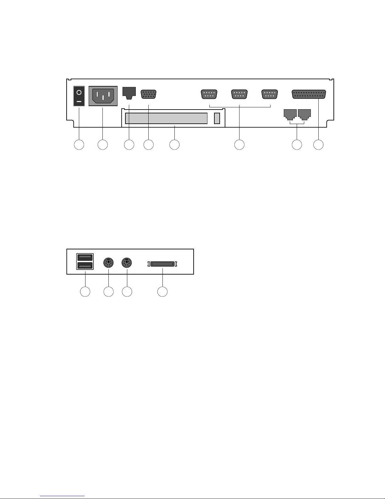
1-5. I/O Outlets
The following diagram shows the I/O arrangement of the QT-7300.
Bottom Panel
1 2 3 4 6 875
1) AC power switch
2) AC inlet
3) Ethernet 10/100 Base-T
4) Second VGA
5) Expansion slot
6) 3 X COM ports
7) 2X Cash Drawers
8) Parallel port
Side Panel
USB
NETVGACOM2COM3COM4PRN
100–230V
K/B
MOUSE FDD
COM1
DRW2 DRW1
4 1 2 3
1) External PS/2 Keyboard
2) External PS/2 mouse
3) External FDD
4) USB
— 5 —
Page 8
2. DISASSEMBLY
To open the case
1. Place the machine up side down.
2. Release the 2 screws of the case management
shroud. Then, remove the case management shroud
4 screws of the lower case.
The lower case
Release the 2 screws.
The case management shroud
3. Release the 3 screws of the lower case.
4. Release the 4 screws and the 12 screws of the lower
case.
Then, open the lower case.
Release the 12 screws.
Release the 3 screws.
Release the 4 screws.
— 6 —
Page 9
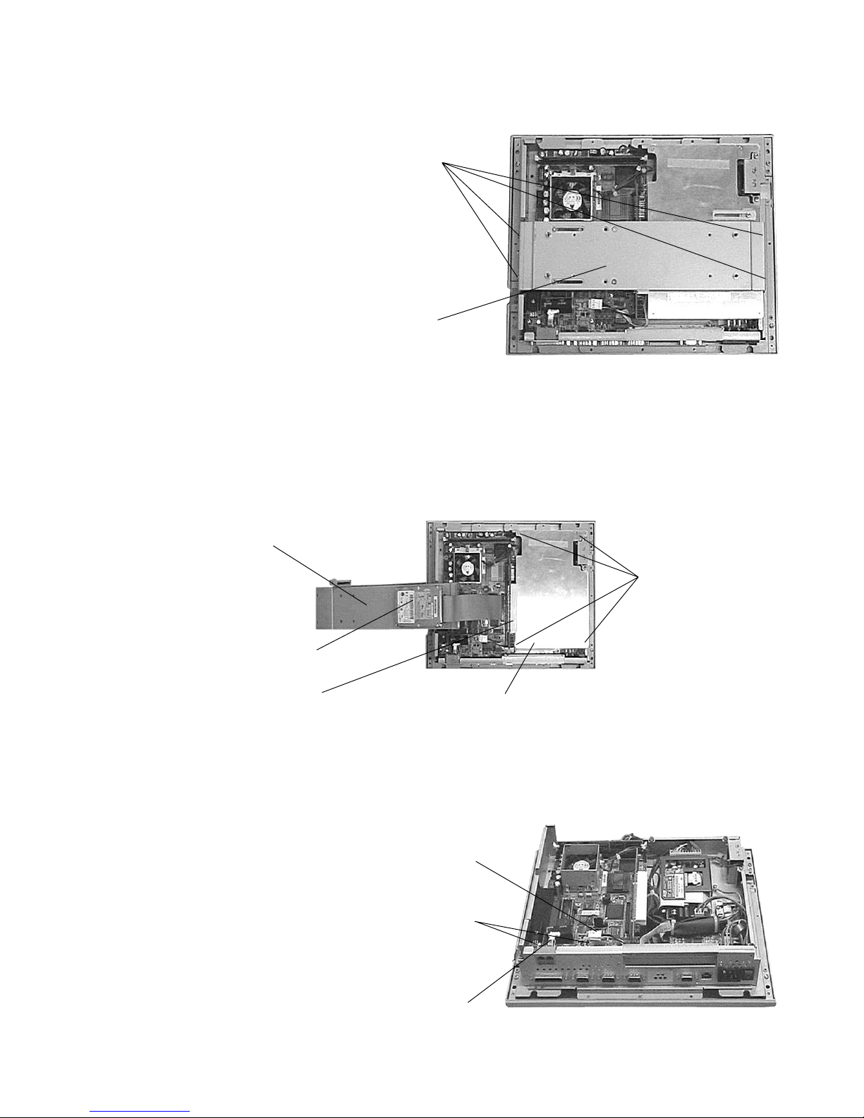
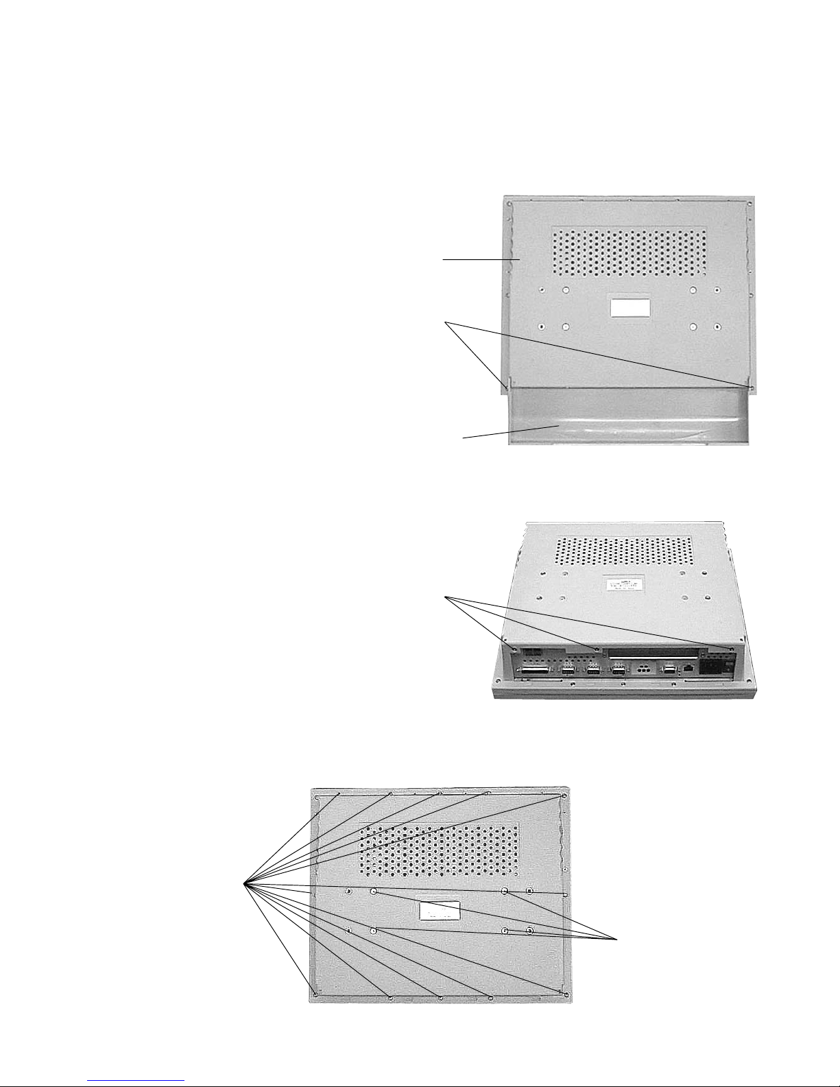
5. Release the 4 screws of the Metal rear bracket.
Then, remove the Metal rear bracket with the HDD
unit.
Release the 4 screws.
The Metal rear bracket with the HDD unit
6. Remove the Riser card from themother board.
Release the 4 screws of the Aluminum separator.
Then, remove the Aluminum separator.
The metal rear bracket with the HDD unit
HDD unit
Remove the Riser card. The Aluminum separator
7. Release the 2 screws of the Drawer drive board and
remove the power connector. Then, remove the
Drawer drive board.
Remove the power connector.
Release the 2 screws.
Releace the 4 screws.
The Drawer drive board
— 7 —
Page 10
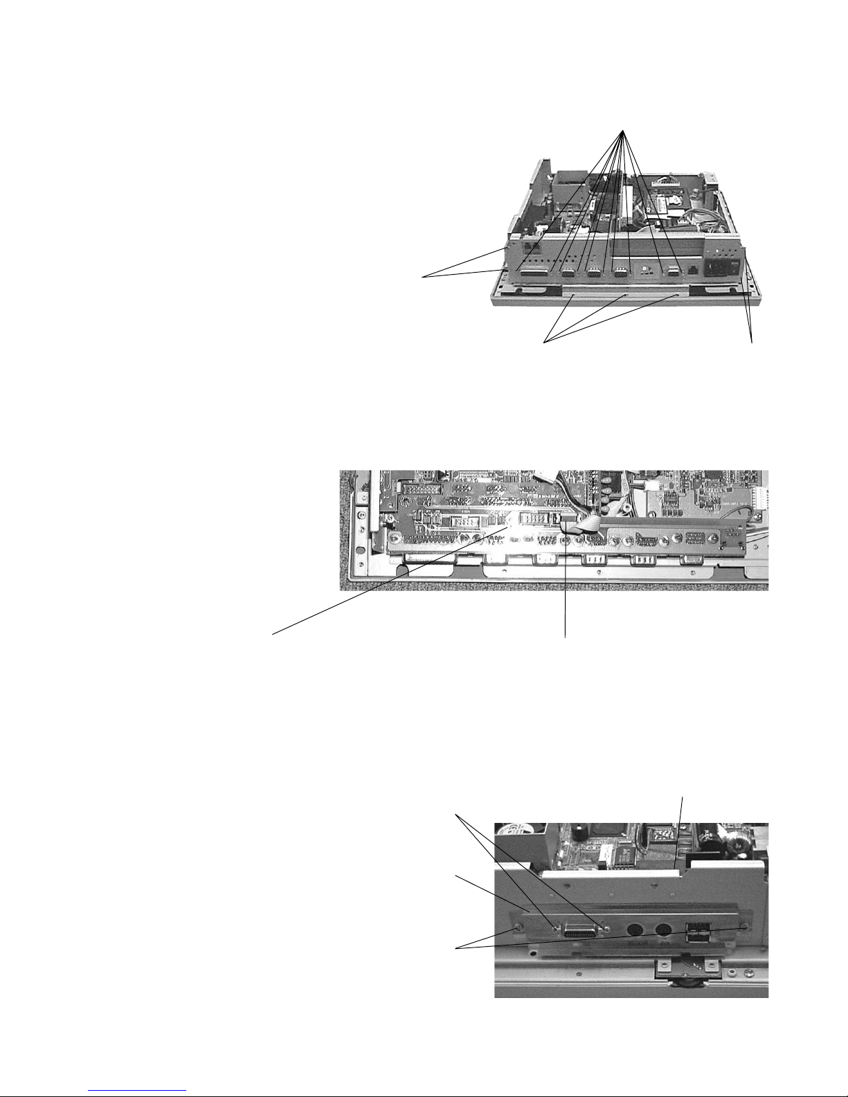
8. Release the 7 screws of the connector panel and
release the 10 connector screws. Then, remove the
connector panel.
Remove 2 screws.
9. Remove the connector from the Touchscreen controller. Then remove the Multi-I/O conversion card.
Remove 10 connector screws.
Remove 3 screws. Remove 2 screws.
Remove the Multi-I/O
conversion card.
10.Release the 2 screws of the side connector cover
and the 2 connector screws. Then, remove the side
connector cover and the KB /Mouse/External FDD
conversion card.
Release the 2 connector screws.
The side connector cover
Release the 2 screws.
Remove the connector from the
Touchscreen controller.
The KB/Mouse/External FDD
conversion card
— 8 —
Page 11
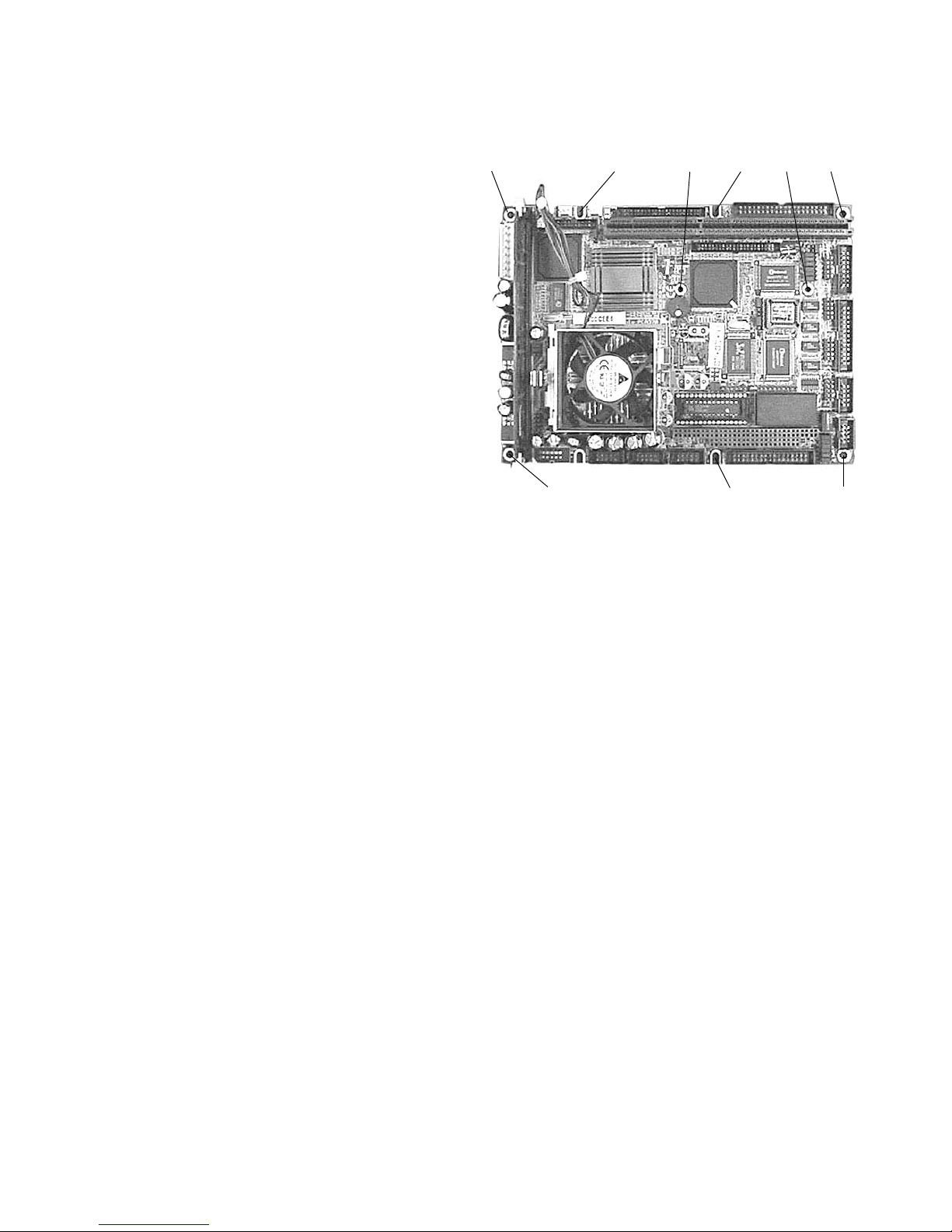
11.Release the 9 screws of the Mother board.
Then, remove the Mother board.
1 2 3 4 56
7 8 9
— 9 —
Page 12
3. INSTALLATION
System main body
LCD Display Contrast adjustment
Large back metal fixtures
Cable management shroud
Large hinge caps
Main prop
Rubber Slip
1
2
3
4
5
6
7
1
2
3
4
5
67
Large back metal fixture
System
main
body
Large hinge
cap
Main
prop
Right or Left
side of main
prop
Unpacking
The QT-7300 along with its accessories are packed in carton box. After unpacking the carton, place the system
on a raised surface and carefully inspect the system for any damage that might have occurred during shipment.
If there are damaged or missing parts, contact your dealer immediately.
Hardware system installation procedure:
1. Attach large back metal fixture(s) to metal part of the main prop on both side with screws. Please refer the
figure “Large back metal fixture” on next page to attach metal fixture with correct direction.
2. Attach metal fixture and main prop to the system main body with screws.
3. Attach large hinge cap(s) to the metal fixture(s) with screws.
NOTES:
1. The QT-7300 do not equip any operating system. An operating system must be loaded first before installing
any software into the QT-7300.
2. Be sure to ground yourself to keep from any static charge when you install the internal components. Use a
grounding wrist strap and place all electronic components in any static-shielded devices. Most electronic
components are sensitive to the static electric charge.
3. Disconnect the power cord from the QT-7300 before any installation. Make sure both the system and the
external devices are turned off and the QT-7300 is properly grounded. The sudden surge of power could ruin
any sensitive components.
4. The brightness of the LCD panel display will decrease with use. However, hours of use will vary depending
on the application environment.
5.
Avoid using sharp objects to operate the touch-screen. Scratches on the touch-screen may cause malfunction
or non-function to the touch-screen
.
— 10 —
Page 13

4. SYSTEM INSTALLATION
This chapter describes the installation of the overall system of the QT-7300. See Chapter 4 for more details on
the motherboard in detail.
The QT-7300 has a Celeron/Pentium III based motherboard with a free PCI slot inside. It already builds in an
Intel Celeron CPU, 64MB of DRAM and a 2.5" HDD. These are all standard and the system is ready to play.
Variety of the I/O ports located at the bottom side and the right side of the chassis are available for customers
to connect external peripheral devices, such as a monitor, serial devices, parallel printer...etc. However, the
interface specification of the peripherals are vary depend on the manufactures and may not applicable to the QT7300 POS system. Please confirm list of the peripheral devices which are test by Casio as the QT-7300 POS
system before you choose the peripherals.
Note: Since all specification and quality of the system are assured by Casio as the QT-7300 POS system, any
local modification of the CPU, DRAM, HDD, jumper setting on the motherboard or system components
by customer will not be applicable for Casio’s guarantee or warranty unless modification are assured
or instructed by Casio.
4-1. CPU
The QT-7300 system already builds in a designated CPU in the socked on the motherboard.
QT-7300: Intel Celeron 566MHz on the motherboard SBC8360-4M
To maintain the CPU, follow the instructions below.
1. Pull the lever sideway away from the socket. Then, raise the lever up to a 90-degree angle.
2. Locate pin 1 at the corner of the CPU socket and align the CPU’s pin 1. Then place the CPU in the socket.
Check the notch on the corner of the CPU and the socket are properly aligned.
3. Press, the lever down to complete the installation. The CPU should always have a Heat Sink with thermal
sheet and a cooling fan attached to prevent overheating.
4. When a CPU is installed, the jumper settings on the motherboard are properly installed as factory default for
the QT-7300 (see Chapter 4 or 5 for CPU jumper settings).
4-2. DRAM
The QT-7300 provides 1 x 168-pin DIMM sockets and 64MB of SDRAM as standard. Maximum system memory
up to 128MB (unbuffered) / 256MB (buffered), respectively. To install the memory module, follow the instructions
below and check the list of DRAM memories tested as QT-7300.
1. The DIMM slots has 2 Notch Keys, so the DIMM memory module can fit in one direction.
2. Insert the DIMM memory module vertically into DIMM slot. Then push in.
3. The plastic clip at the side of the DIMM slot will automatically close.
The system is able to detect the new memory size automatically and it is not necessary to change the system
configuration after installation.
— 11 —
Page 14
4-3. HDD
The standard QT-7300 already builds in a 2.5" hard disk drive. To maintain the HDD, follow the installation
instructions below and check the list of HDD tested as the QT-7300.
1. Take out the screws, the IDE cable and remove the HDD.
2. Reinstall the new HDD on the bracket. The four rubber stands act as cushions to lessen the vibration which
usually causes damage to a mechanical device like a HDD.
3. Connect the IDE cable to the HDD. Match pin 1 of the HDD and the pin 1 of the cable.
4-4. Serial Ports
QT-7300 four onboard serial ports. Since the touch screen system requires one dedicated serial port interface
and COM1 is assigned for it, so that COM1 is not available for users. For the QT-7300, COM2 and COM4 are
RS-232, selected by jumpers. Each serial port is with +5V/+24V and +12V/+24V power capabilities on pin 1 and
pin 9, ready to accommodate a wide array of serial devices. COM2 to COM4 are all D-SUB 9-pin connectors.
4-5. Parallel Port
The printer interface is a 25-pin D-SUB connector located on the bottom side. To connect any parallel device,
just plug in the device connector to the 25pin D-SUB. There are variety of parallel port peripherals in the market
and interface specification vary depending on the peripherals. The peripherals which have been confirmed with
the QT-7300 terminals are listed in the Appendix and others may not be supported. Please confirm connectivity
of each peripherals before install to the customer site.
4-6. VGA
The QT-7300 has an analog RGB interface connector installed on the bottom side. It is able to connect to an
expansion CRT monitor, and the system can display on both the LCD display and the CRT individually or
simultaneously. However, as the LCD display adapted is of the resolution of 800 x 600, therefore, to support a
CRT monitor simultaneously, the CRT’s VGA resolution has to be set to 800 x 600, too. It can also support CRT
maximum resolution of up to 1600 x 1200 with 8bit on Dual-Display Mode colors. Also, an automatic horizontal
frequency detective type CRT is only approved.
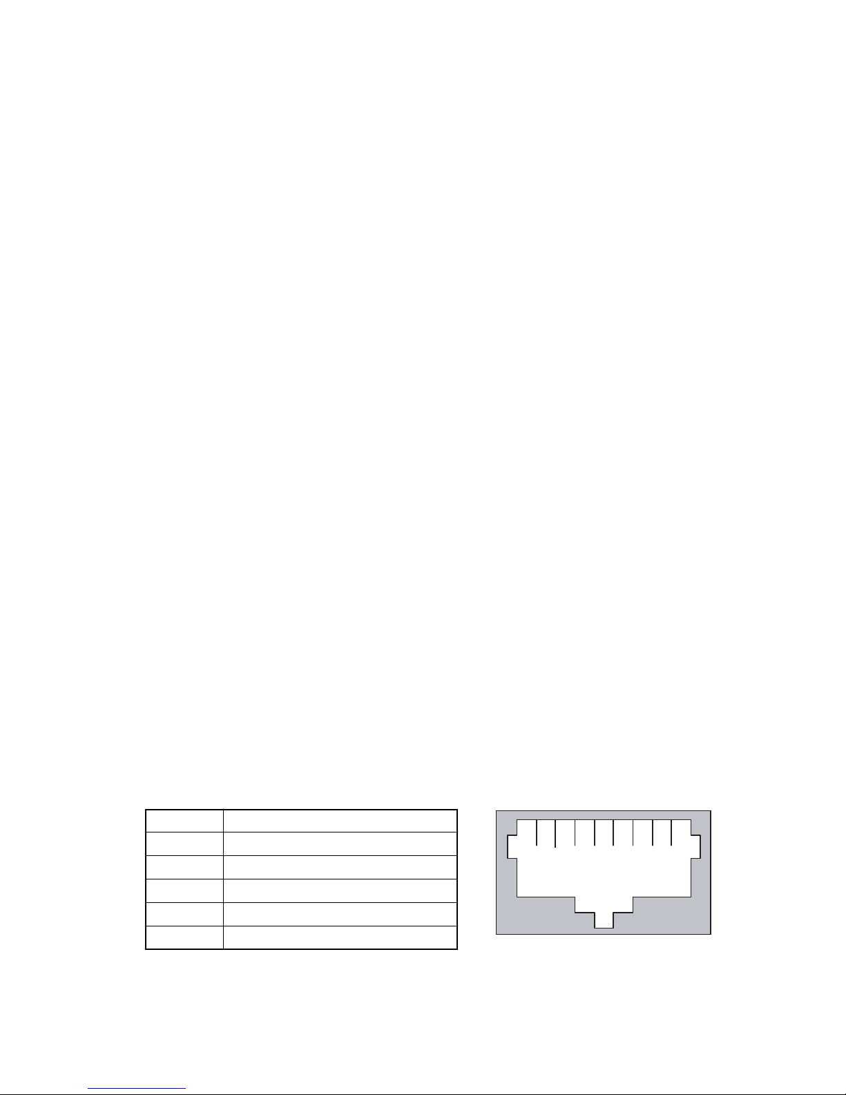
4-7. Ethernet
The QT-7300 provide a high performance Ethernet (RJ-45) interface. For network connection, just plug in one
end of cable of a 10/100-Base-T hub to the standard Ethernet phone jack. The pin assignment of the RJ-45 is
listed below;
RJ-45 Connector Pin Assignment
Pin Description
1 Tx+ (Data transmission positive)
2 Tx- (Data transmission negative)
3 Rx+ (Data reception positive)
6 Rx- (Data reception negative)
others Not use
15842736
RJ-45
— 12 —
Page 15
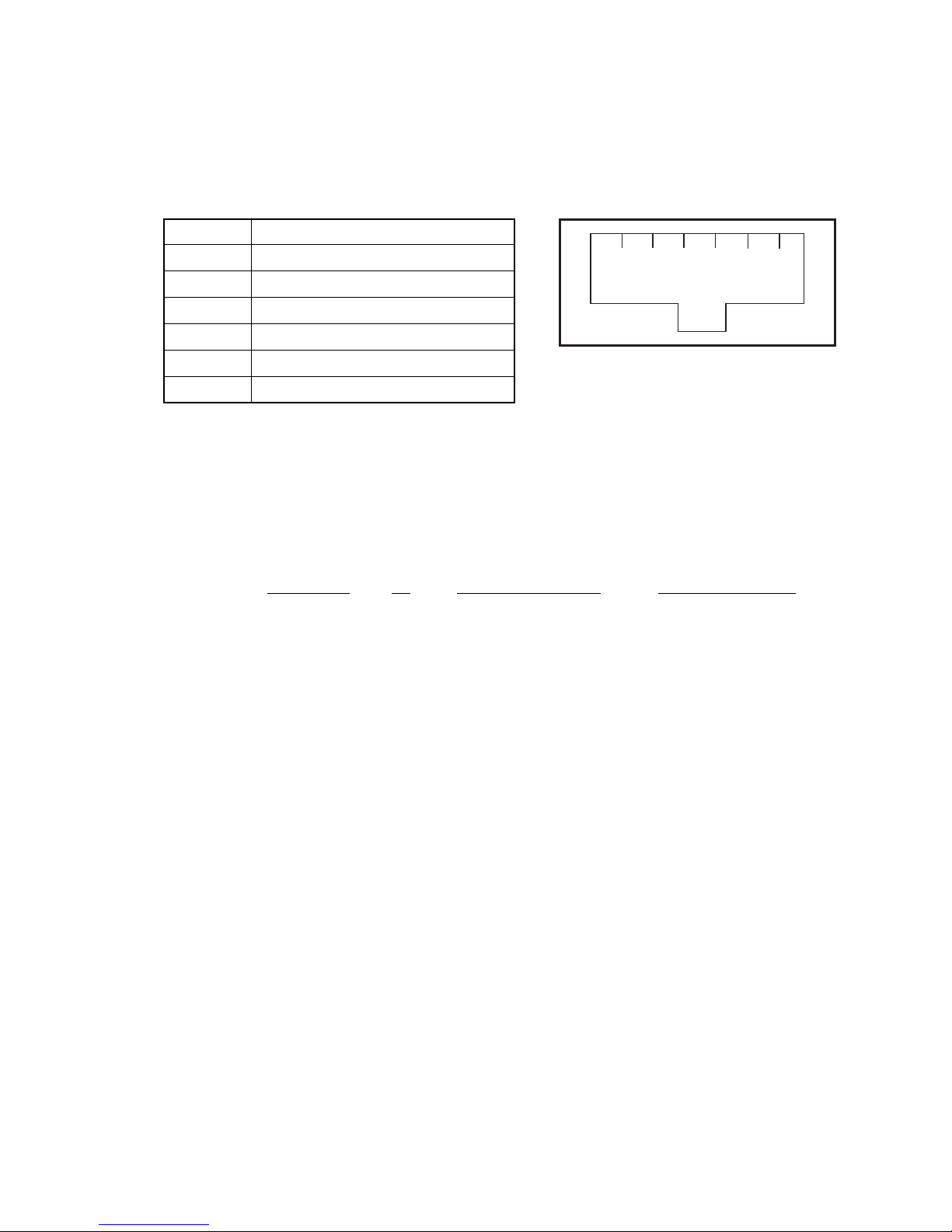
4-8. Cash Drawer
The QT-7300 provides two Cash Drawer interface. Cash Drawers are assigned as one of I/O in this system and
controlled by the Drawer port on the motherboard (SBC8360-4M).
The pin assignment for the Cash Drawer connector is as follows.
Cash Drawer connector Pin Assignment
Pin Description
1FG
146325
2 Out Switch
3 Read Switch
4 +24V
5NC
6 GND
4-8-1. Cash Drawer control Software Programming
The Cash Drawer is assigned as one of I/O device in the system. The I/O address assigned for the Cash Drawers
123h. The QT-7300 can support two Cash Drawers and each Cash Drawers can be controlled respectively by
output or input data to this I/O address. The open/close status of drawers also can be read by reading this I/O
address. Following is software programming method for Casio standard Cash Drawer model DL-2765, DL-2909
and DL-3615.
I/O Address Bit Output Data to Open Input data for status
Drawer A 123 0 01h FEh (open)
Drawer B 123 1 02h FDh (open)
Example program; < Drawer A open >
Out 123h, 01h : Drawer A open signal on
< 100 ms timer > : Open signal on 100 ms
Out 123h, 00h : Drawer A open signal off
Example program; < Read Drawer open status >
Input 220h : Read Drawer open status
If data is FFh: Drawer A , B closed
If data is FEh: Drawer A is open, Drawer B is closed.
If data is FDh: Drawer A is closed, Drawer B is open.
If data is FCh: Drawer A is open, Drawer B is open.
Note: 1) Drawer open signal on time is 100 ms.
2) Do not open Drawer A and B at same time (Output data 03). If two drawers were open at same time,
it may cause damage on system power supply.
— 13 —
Page 16

4-9. Keyboard
The QT-7300 provides a standard PS/2 keyboard connector located at the side panel. If the user would like to
use AT keyboard interface, a conversion cable is also provided to make this connection.
4-10. PS/2 Mouse
The QT-7300 has one PS/2 Mouse connector located at the right side. A simple plug-in will make the connection.
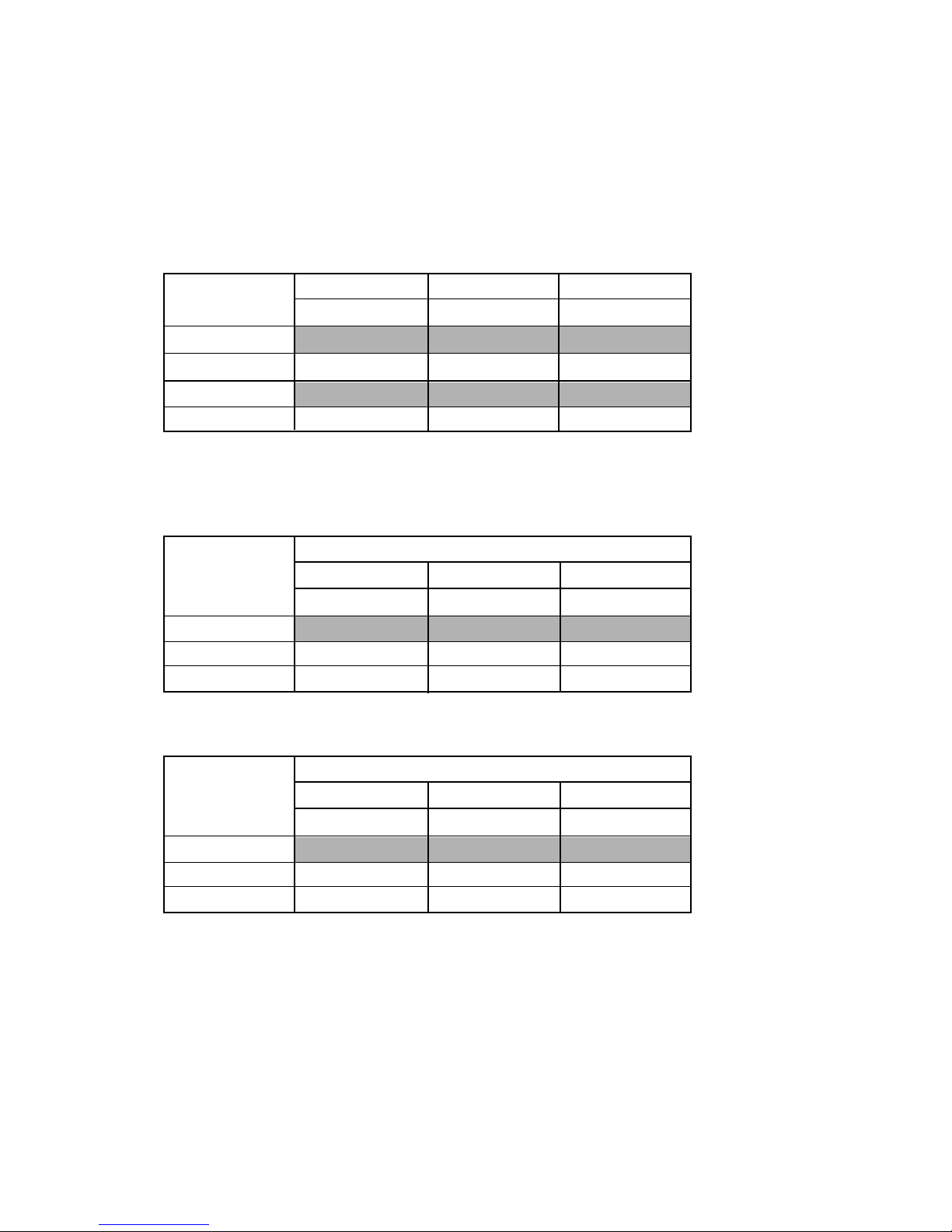
4-11. External FDD
The QT-7300 does not build in any floppy disk drive into the main system. Rather, it provides a FDD interface
located at the side panel. An external FDD cable is provided to connect a standard 3.5" FDD to the system for
system O/S and application software installation. Its pin position and pin assignment is listed as follows;
External FDD Pin Assignment
Pin Description Pin Description
P 1 SIDE1- P 14 WPTP 2 RDATA- P 15 TRK0P 3 GND P 16 GND
P 4 GND P 17 WGATEP 5 GND P 18 GND
P 6 WDATA- P 19 NC
P 7 REDWC- P 20 STEPP 8 NC P 21 DIRP 9 NC P 22 MOTE0P 10 DRVS0- P 23 NC
P 11 FDDDVcc P 24 DSKCHGP 12 FDDDVcc P 25 NC
P 13 INDEX- P 26 FDDDVcc
— 14 —
Page 17

4-12. Expansion Slot
The QT-7300 provides a free PCI expansion slot to accommodate a PCI device at a given time. The expansion
card can be plugged into the riser card which is plugged in the onboard PCI/ISA slot as standard. Due to the
compact space design, a half-size expansion card can be adapted. To use the PCI expansion, follow the
installation instructions below;
1. Unscrew the metal slip located inside the expansion outlet.
2. Plug a PCI card into the PCI slot on the riser card and fix the expansion card by screwing it to the metal front
compartment. All the connectors of the expansion card will come out from the expansion outlet on the bottom
side of the chassis for further cable connection.
4-13. System O/S and Software Installation
The QT-7300 is not equipped with any operating system. It builds in a 2.5" HDD as memory storage device. As
both devices are built in the system chassis, to load Win98/Win98SE or Win2000 O/S or application software
into the system, an external device is needed to act as a bridge. There are three major ways to load software
into the system.
1. Use an external FDD: Attach a 3.5" FDD to the external FDD port via the provided external FDD
cable. The 26-pin FDD connector is to be plugged in to the system FDD
connector; the 34-pin standard 3.5" FDD signal connector and the 4-pin FDD
power connector are to connect to the standard 3.5" FDD. Then, configure the
system BIOS setup and insert a 3.5" disk containing necessary software and
start the installation.
2. Use Ethernet: After install the O/S and necessary network utilities, download application
software from the network.
3. Use External CD-ROM/HDD: To use an external CD-ROM or HDD for software installation, an optional P-
IDE device is needed. The P-IDE device is a converter to convert the parallel
port to the IDE interface.
— 15 —
Page 18

4-14. Award BIOS Setup
>
Starting Award BIOS Setup
As POST executes, the following appears
Hit <DEL> if you want to run SETUP
Press <Del> to run Award BIOS Setup.
4-14-1. Award BIOS Setup Main Menu
When you enter the Award BIOS Setup Utility, the main menu will appear on the screen as follows. Use the arrow
keys to move among the items and press <Enter> to accept and enter into the sub-menu.
< Screen shows all default setting
ROM PCI/ISA BIOS (2A69KA5C)
CMOS SETUP UTILITY
AWARD SOFTWARE, INC.
STANDARD COMS SETUP
BIOS FEATURES SETUP
CHIPSET FEATURES SETUP
POWER MANAGEMENT SETUP
PNP/PCI CONFIGURATION SETUP
LOAD BIOS DEFAULTS
LOAD SETUP DEFAULTS
ESC : Quit
F10 : Save & Exit Setup
Time, Date, Hard Disk Type...
INTEGRATED PERIPHERALS
SUPERVISOR PASSWORD
USER PASSWORD
IDE HDD AUTO DETECTION
SAVE & EXIT SETUP
EXIT WITHOUT SAVING
↑ ↓ → ← : Quit
(Shift) F2 : Save & Exit Setup
— 16 —
Page 19

4-14-2. Setup
>
The Award BIOS Setup options described in this section are selected by choosing the appropriate high-level icon
from the Award BIOS Setup main menu selection screen.
Default setting for the QT-7300 is described in < > next to each option. ( i.e. <AUTO> )
4-14-2-1. Standard CMOS Setup
< Screen shows all default setting
ROM PCI/ISA BIOS (2A69KA5C)
STANDARD CMOS SETUP
AWARD SOFTWARE, INC.
Date (mm:dd:yy) : Tue, Oct 27 1999
Time (hh:mm:ss) : 18 : 56 : 41
HARD DISKS
Primary Master
Primary Slave
Secondary Master
Secondary Slave
Drive A : 1.44M, 3.5 in
Drive B : None
Video : EGA/VGA
Halt On : All Errors
ESC : Quit
F1 : Help
Type
: Auto
: None
: None
: None
SIZE
0
0
0
0
CYLS
0
0
0
0
↑ ↓ → ← : Select Item
(Shift) F2 : Change Color
HEAD
PRECOMP
0
0
0
0
PU/PD/+/- : Modify
LANDZ
0
0
0
0
BASE Memory
Extended Memory
Other Memory
Total Memory
0
0
0
0
SECTOR
0
0
0
0
:
:
:
:
MODE
AUTO
----
----
----
640K
64512K
384K
65536K
• Date, Day and Time Configuration
Select the Standard option. Select the Date and Time icon. The current values for each category are
displayed. Enter new values through the keyboard.
• Primary Master
• Primary Slave
• Secondary Master
< Auto>
< None>
< None>
• Secondary Slave
< None>
Select one of these hard disk drive icons to configure the drive named in the option. A scrollable screen
that lists all valid disk drive types is displayed. Select the correct type and press <Enter>. The Award
BIOS is able to detect the IDE drive parameters automatically and report them on this screen. To
enable this auto-detect function, just select the drive type Auto.
NOTE: Secondary drives are not support.
• Drive A
• Drive B
< 1.44MB, 3.5inch>
< Not Installed >
Move the cursor to these fields via and select the floppy type. The settings are 360KB 5.25 inch, 1.2
MB 5.25 inch, 720KB 3.5 inch, 1.44 MB 3.5 inch, or 2.88 MB 3.5 inch.
• Video
<EGA/VGA>
The category selects the type of adapter used for the primary system modify that must match your video
display card and monitor.
— 17 —
Page 20

• Error Halt
>
<All errors>
The category determines whether the computer will stop if an error is detected during power up.
• Memory
The category is display-only which is determined by POST (Power On Self Test) of the BIOS.
4-14-2-2. BIOS Features Setup
< Screen shows all default setting
ROM PCI/ISA BIOS (2A69KA5C)
BIOS FEATURES SETUP
AWARD SOFTWARE, INC.
Virus Warning : Disabled
CPU Internal Cache : Enabled
External Cache : Enabled
CPU L2 Cache ECC Check : Enabled
Processor Number Feature : Enabled
Quick Power On Self Test : Enabled
Boot Sequence : A,C,SCSI
Video BIOS Shadow : Enabled
C8000-CBFFF Shadow : Disabled
CC000-CFFFF Shadow : Disabled
D0000-D3FFF Shadow : Disabled
D4000-D7FFF Shadow : Disabled
D8000-DBFFF Shadow : Disabled
DC000-DFFFF Shadow : Disabled
Swap Floppy Drive : Disabled
Boot Up Floppy Seek : Disabled
Boot Up NumLock Status : On
Gate A20 option : Fast
Typematic Rate Setting : Disabled
Typematic Rate (Chars/Sec) : 6
Typematic Delay (msec) : 250
LCD Type : (Type 8) 800x600 TFT
VGA Expansion (Full Screen) : Enable
Display Type During POST : Both
Display Type After POST : Both
Security Option : Setup
PCI/VGA Palette Snoop : Disabled
Assign IRQ for VGA : Enabled
OS Select for DRAM > 64MB : Non-OS2
Report No FDD for Win95 : Yes
ESC : Quit
F1 : Help
F5 : Old Values
F6 : Load BIOS Defaults
↑ ↓ → ← : Select Item
PU/PD/+/- : Modify
(Shift) F2 : Color
F7 : Load Setup Defaults
• Virus Warning
• CPU Internal Cache / External Cache
<Disabled>
< Enabled >
These two speed up memory access. However, it depends on the CPU/chipset design.
• CPU L2 Cache ECC Checking
When enabled, this allows ECC checking of the CPU's L2 cache.
• Quick Power On Self Test
• Boot Sequence
< A,C,SCSI >
This option sets the sequence of boot drives either floppy drive A or hard disk drive C or CDROM that
Award BIOS attempts to boot from after POST completes
• Swap Floppy Drive
This option enables the floppy swap function. The setting is Enable or Disable.
• Boot Up Floppy Seek
This option enables Award BIOS seek on floppy drive A before booting the system. The settings is
Enabled or Disabled.
• Boot Up NumLock Status
This option enables and disables the numberlock function of the keypad.
• Gate A20 option
< Fast >
< Enabled >
< Enabled >
< Disabled >
< Disabled >
< On >
— 18 —
Page 21

• Typematic Rate Setting
This determines the typematic rate of the keyboard.
< Disabled >
• Typematic Rate (Chars/Sec)
This option refers to the number of characters the keyboard can type per second.
• Typematic Delay (msec)
This option sets the display time interval from the first to the second character when holding a key.
• Security Option
This item allows you to limit access to the system and Setup, or just to Setup.
• PCI/VGA Palette Snoop
Some non-standard VGA display cards may not show colors properly.
• Assign IRQ for VGA
Enables or disables VGA's IRQ assignment.
• OS Select for DRAM > 64MB
This segment is specifically created for OS/2 when DRAM is larger than 64MB.
• Report No FDD for Win98/98SE/2000
This option allows Windows98/98SE/2000 to share IRQ6 (assigned to a floppy disk drive) with other
peripheral in cash the drive is not existing.
• Video ROM BIOS Shadow
Video shadowing increases the video speed by copying the video BIOS into RAM.
• C8000-CBFFF Shadow
• CC000-CFFFF Shadow
• D0000-D3FFF Shadow
< Setup >
< Enabled >
< 6 >
< 250 >
< Disabled >
< Non-OS2 >
< Yes >
< Enabled >
< Disabled >
< Disabled >
< Disabled >
• D4000-D7FFF Shadow
• D8000-DBFFF Shadow
• DC000-DFFFF Shadow
These options determine whether optional ROM will be copied t RAM by 16K byte or 32K byte per/unit.
OnBoard VGA Function
The following options allow the overriding of the VGA BIOS setting integrated in the core chipset of
SBC8360-4M.
• LCD Type
Although the system chipset already supports VGA and LCD alike, BIOS Features Setup still expands
this feature further with the option to set any of 15 LCD types.
• VGA Expansion (Full Screen)
This option allows you to enlarge application screens to full screen scale onto your display.
However this opton is not inversely compatible, rendering no change when applications screens have
resolutions larger than the display resolution.
• Display Type During POST
• Display Type After POST
This item configures the viewing area for the POST sequence. When configured to the incorrect display
setting or BOTH, it blankets the POST sequence from being viewed. If you select Default this option
is useless and follows the VGA BIOS setting.
< (Type 8) 800x600 TFT >
< Disabled >
< Disabled >
< Disabled >
< Enabled >
< Both >
< Both >
— 19 —
Page 22

4-14-2-3. Chipset Features Setup
>
< Screen shows all default setting
ROM PCI/ISA BIOS (2A69KA5C)
CHIPSET FEATURES SETUP
AWARD SOFTWARE, INC.
SDRAM RAS-to-CAS Delay : 3
SDRAM RAS Precharge Time : 3
SDRAM CAS Latency Time : Auto
SDRAM Precharge Control : Disabled
DRAM Data Integrity Mode : Non-ECC
System BIOS Cacheable : Disabled
Video BIOS Cacheable : Disabled
Video RAM Cacheable : Disabled
8 bit I/O Recovery Time : 1
16 bit I/O Recover Time : 1
CPU Warning Temperature : Disabled
Current System1 Temp : 35 °C/ 95 °F
Current System2 Temp : 0 °C/ 32 °F
Current CPU Temperature : 50 °C/112 °F
Current FAN1 Speed : 6136 RPM
Current FAN2 Speed : 0 RPM
Current FAN3 Speed : 0 RPM
Vcore : 1.68 V VTTP : 1.48 V
VCC : 3.32 V + 5 V : 5.18 V
+12 V : 12.28 V
Memory Hole At 15M-16M : Disabled
Passive Release : Enabled
Delayed Transaction : Disabled
AGP Aperture Size (MB) : 64
ESC : Quit
F1 : Help
F5 : Old Values
↑ ↓ → ← : Select Item
PU/PD/+/- : Modify
(Shift) F2 : Color
F6 : Load BIOS Defaults
F7 : Load Setup Defaults
• SDRAM RAS-to-CAS Delay
< 3 >
You can select RAS-to-CAS delay in HCLKs 2 or 3. The board designer should set the values in this
field, depending on the DRAM installed. Do not change the values in this field unless you change
specifications of the installed DRAM or installed CPU.
• SDRAM RAS Precharge Time
< 3 >
When synchronous DRAM is installed, the number of clock cycles of RAS precharge time depends on
the DRAM timing. Do not reset this field from the default value specified by system designer.
• SDRAM CAS Latency Time
You can select CAS latency time in HLCKs 2, 3 or Auto. The board designer should set the values in
this field, depending on the DRAM installed. Do not change the values in this field unless you change
specifications of the installed DRAM or installed CPU.
• SDRAM Precharge Control
• DRAM Data Integrity Mode
This option sets the data integrity mode of the DRAM installed in the system.
• System BIOS Cacheable
Selecting Enables allows caching of the system BIOS ROM at F0000h-FFFFh, resulting in better
system performance. However, if any program writes to this memory area, a system error may result.
• Video BIOS Cacheable
This item allows you to change the Video BIOS location from ROM to RAM. Video shadow wil increase
the video speed.
< Auto >
< Disabled >
< Non-ECC >
< Disabled >
< Disabled >
— 20 —
Page 23

• Video RAM Cacheable
< Disabled >
Selecting Enabled allows caching of the Video BIOS ROM at C0000h to C7FFFh, resulting in better
video performance. However, if any program writes to this memory area, a system error may result.
• 8 bit I/O Recovery Time
• 16 bit I/O Recover Time
< 1 >
< 1 >
The I/O recovery mechanism adds bus clock cycles between PCI-originated I/O cycles to the ISA bus.
This delay takes place because the PCI bus is so much faster than the ISA bus.
These two fields let you add recovery time (in bus clock cycles) for 16/8 - bit I/O.
• Memory Hole At 15M-16M
< Disabled >
You can reserve this area of system memory for ISA adapter ROM. When this area is reserved, it
cannot be cached. He user information of peripherals that need to use this area of system memory
usually discusses their memory requirements.
• Passive Release
< Enabled >
When enabled, CPU to PCI accesses are allows during passive release. Otherwise, the arbiter only
accept another PCI master access to local DRAM.
• Delayed Transaction
< Disabled >
The chipset has an embedded 32-bit posted write buffer to support delay transactions cycles. Select
Enabled to support compliance with PCI specification version 2.1.
• AGP Aperture Size (MB)
< 64 >
The field sets aperture size of the graphics. The aperture is portion of the PCI memory address range
dedicated for graphics memory address space. Host cycles that hit the aperture range are forwarded
to the AGP without any translation.
• CPU Warning Temperature
< Disabled >
This option lets you set the CPU temperature limit where the system will produce a warning indicating
CPU temperature has already exceeded.
• Current System1 Temp (35 °C/ 95 °F)
• Current System2 Temp (0 °C/ 32 °F)
• Current CPU Temperature (50 °C/112 °F)
These ready-only field reflect the function of the hardware thermal sensor that monitors the chio blocks
and system temperature to ensure the system is stable.
• Current FAN1 Speed (6136 RPM)
• Current FAN2 Speed (0 RPM)
• Current FAN3 Speed (0 RPM)
These option and ready-only field show the current speeds in RPM (revolution per minute) for the CPU
fan and chassis fan as monitored by the hardware monitoring IS.
• VCore (1.68 V) / VTTP (1.48 V) / VCC (3.32 V) / + 5 V (5.18 V) / +12 V (12.28 V)
These option and ready-only field show the current voltages in the voltage regulators and power supply
as monitored by the hardware monitoring IS.
— 21 —
Page 24

4-14-2-4. Power Management Setup
>
< Screen shows all default setting
ROM PCI/ISA BIOS (2A69KA5C)
POWER MANAGEMENT SETUP
AWARD SOFTWARE, INC.
ACPI function : Disabled
Power Management : User Define
PM Control by APM : Yes
Video off Method : V/H SYNC + Blank
Video off After : Standby
Modem Use IRQ : 3
Doze Mode : Disabled
Standby Mode : Disabled
Suspend Mode : Disabled
** Reload Global Timer Events **
IRQ[3-7,9-15],NMI Disabled
Primary IDE 0 : Disabled
Primary IDE 1 : Disabled
Secondary IDE 0 : Disabled
Secondary IDE 1 : Disabled
Floppy Disk : Disabled
Serial Port : Enabled
Parallel Port : Disabled
HDD Power Down : Disabled
Throttle Duty Cycle : 62.5%
PCI/VGA Act-Monitor : Disabled
Soft-Off by PWR-BTTN : Instant-Off
Wake Up on LAN : Enabled
IRQ 8 Break Suspend : Disabled
ESC : Quit
F1 : Help
F5 : Old Values
↑ ↓ → ← : Select Item
PU/PD/+/- : Modify
(Shift) F2 : Color
F6 : Load BIOS Defaults
F7 : Load Setup Defaults
• ACPI function
< Disabled >
This item allows you to enable/disable the Advanced Configuration and Power Management (ACPI).
• Power Management
This option allows you to select the type (or degree) of power saving for Doze, Standby
• PM Control by APM
< User Define >
< Yes >
If Advanced Power Management (ACPI) is installed on your system, selecting Yes gives better power
savings.
• Video off Method
< V/H SYNC + Blank >
Determines the manner in which the monitor is blanked.
• Video off After
< Standby >
As the system moves from lesser to grater power-saving modes, select the mode in which you want
the monitor to blank off.
• Modem Use IRQ
• Doze Mode
< 3 >
< Disabled >
After the selected period of system inactivity (1 minute to 1 hour), the CPU clock runs at slower speed
while all other devices still operate at full speed.
• Standby Mode
< Disabled >
After the selected period of system inactivity (1 minute to 1 hour), the fixed disk drive and the video shut
off while all other devices still operate at full speed.
• Suspend Mode
< Disabled >
After the selected period of system inactivity (1 minute to 1 hour), all devices except the CPU shut off.
— 22 —
Page 25

• HDD Power Down
After the selected period of drive inactivity (1 to 15 minute), the hard disk drive powers down while all
other devices remain active.
< Disabled >
• Throttle Duty Cycle
When the system enters Doze mode, the CPU clock runs only part of the time. You must select the
percent of time that the clock runs.
• PCI/VGA Act-Monitor
When Enabled, any vide activity restarts the global timer for Standby mode.
• Soft-Off by PWR-BTTN
This only works with system using an ATX power supply. It also allows user to define the type of soft
power OFF sequence the system will follow.
• Wake Up on LAN
All input signal on the network awakens the system from a soft-off state.
• IRQ 8 Break Suspend
You can turn on or off monitoring of IRQ8 (the Real Time Clock) so it does not awaken the system form
Suspend mode.
** Reload Global Timer Events **
When Enabled, an event occurring on each device listed below restarts the global time for Stanby
mode.
• IRQ[3-7,9-15],NMI
• Primary IDE 0
• Primary IDE 1
< 62.5% >
< Disabled >
< Instant-Off >
< Enabled >
< Disabled >
< Disabled >
< Disabled >
< Disabled >
• Secondary IDE 0
• Secondary IDE 1
NOTE: Secondary drives are not support.
• Floppy Disk
• Serial Port
• Parallel Port
< Disabled >
< Disabled >
< Disabled >
< Enabled >
< Disabled >
— 23 —
Page 26

4-14-2-5. PCI / Plug and Play Setup
>
PNP OS Installed : No
Resources Controlled By : Auto
Reset Configuration Data : Disabled Assign IRQ For USB : Enabled
< Screen shows all default setting
ROM PCI/ISA BIOS (2A69KA5C)
PNP/PCI CONFIGRATION
AWARD SOFTWARE, INC.
Onboard Ethernet BootROM : Disabled
ESC : Quit
F1 : Help
F5 : Old Values
F6 : Load BIOS Defaults
F7 : Load Setup Defaults
• PNP OS Installed
Select Yes the system operating environment is Plug-and-Play aware (e.g., Win98/98SE/2000).
• Resources Controlled By
The Award Plug and Play BIOS can automatically configure all the boot and Plug and Play-compatible
devices. If you select Auto, all the interrupt request (IRQ), DMA assignment, and used DMA field
disappear, as the BIOS automatically assigns them.
• Reset Configuration Data
Normally, you leave this field Disabled. Select Enabled to reset Extended System Configuration Data
(ESCD) when you exit Setup if you have installed a new add-on and system reconfiguration has caused
such a serious conflict that the operating cannot boot.
• IRQ 3 Assigned to
• IRQ 4 Assigned to
• IRQ 5 Assigned to
• IRQ 7 Assigned to
< No >
< Auto >
< Disabled >
< Legacy ISA >
< Legacy ISA >
< PCI/ISA PnP >
< Legacy ISA >
↑ ↓ → ← : Select Item
PU/PD/+/- : Modify
(Shift) F2 : Color
• IRQ 9 Assigned to
• IRQ 10 Assigned to
• IRQ 11 Assigned to
• IRQ 12 Assigned to
• IRQ 14 Assigned to
< PCI/ISA PnP >
< Legacy ISA >
< Legacy ISA >
< PCI/ISA PnP >
< PCI/ISA PnP >
— 24 —
Page 27

• IRQ 15 Assigned to
< PCI/ISA PnP >
When resources are controlled manually, assign each system interrupt as one of the following types,
depending on the type of device using the interrupt:
1. Legacy ISA Devices compliant with the original PC AT bus specification, requiring a specific
interrupt (such as IRQ4 for serial port 1).
2. PCI/ISA PnP Devices compliant with the Plug and Play standard, whether designed for PCI or ISA
bus architecture.
• DMA 0 Assigned to
• DMA 1 Assigned to
• DMA 3 Assigned to
• DMA 5 Assigned to
• DMA 6 Assigned to
• DMA 7 Assigned to
< PCI/ISA PnP >
< PCI/ISA PnP >
< PCI/ISA PnP >
< PCI/ISA PnP >
< PCI/ISA PnP >
< PCI/ISA PnP >
When resources are controlled manually, assign each system DMA channel as one of the following
types, depending on the type of device using the DMA channel:
Legacy ISA Devices compliant with the original PC AT bus specification, requiring a specific DMA
channel.
PCI/ISA PnP Devices compliant with the Plug and Play standard, whether designed for PCI or ISA bus
architecture.
• Used MEM base addr
< N/A >
Select a base address for the memory area used by any peripheral that requires high memory.
• Assign IRQ For USB
< Enabled >
This item allows you to assign IRQ for the USB interface.
• Onboard Ethernet BootROM
< Disabled >
The BIOS of SBC8360-4M includes Boot ROM for Novell.
— 25 —
Page 28

4-14-2-6. Integrated Peripheral Setup
>
ROM PCI/ISA BIOS (2A69KA5C)
< Screen shows all default setting
INTEGRATED PERIPHERALS
AWARD SOFTWARE, INC.
IDE HDD Block Mode : Enabled
UART Mode Select : Normal
IDE Primary Master PIO : Auto
IDE Primary Slave PIO : Auto
IDE Secondary Master PIO : Auto
IDE Secondary Slave PIO : Auto
IDE Primary Master UDMA : Auto
Onboard Parallel Port : 378H/IRQ7
Parallel Port Mode : SPP
IDE Primary Slave UDMA : Auto
IDE Secondary Master UDMA : Auto
IDE Secondary Slave UDMA : Auto
On-Chip Primary PCI IDE : Enabled
Onboard Parallel Port 3 : 3E8H/IRQ10
Onboard Parallel Port 4 : 2E8H/IRQ11
On-Chip Secondary PCI IDE : Enabled
USB Keyboard Support : Enabled
Init Display First : PCI/ISA
POWER ON Function :
Onboard FDC Controller : Enabled
Onboard Serial Port 1 : 3F8H/IRQ4
Onboard Serial Port 2 : 2F8H/IRQ3
BUTTON ONLY
ESC : Quit
F1 : Help
F5 : Old Values
↑ ↓ → ← : Select Item
PU/PD/+/- : Modify
(Shift) F2 : Color
F6 : Load BIOS Defaults
F7 : Load Setup Defaults
The four items related to the WDT describe the set up of the Watchdog Timer (WDT), please refer to the 4-15
for details.
• IDE HDD Block Mode
Block mode is also called block transfer, multiple commands, or multiple sector read/write. If your IDE
< Disabled >
hard drive supports block mode (most new drives do ), select Enabled for automatic detection of the
optional number of block read/write per sector the drive can support.
• IDE Primary Master PIO
• IDE Primary Slave PIO
• IDE Secondary Master PIO
• IDE Secondary Slave PIO
< Auto >
< Auto >
< Auto >
< Auto >
The four IDE PIO (Programmed Input/Output) field let you set a PIO mode (0-4) for each of four IDE
devices that the onboard IDE interface supports. Modes 0 though 4 provide successively increased
performance. In Auto mode, the system automatically determines the best mode for each device.
NOTE: Secondary drives are not support.
• IDE Primary Master UDMA
• IDE Primary Slave UDMA
• IDE Secondary Master UDMA
• IDE Secondary Slave UDMA
< Auto >
< Auto >
< Auto >
< Auto >
Ultra DMA/33 implementation is possible only if your IDE hard drive supports it and the operating
environment includes a DMA driver (Windows98 or a third-party IDE bus master driver). If your hard
drive and your system software both support Ultra DMA/33, select Auto to enable BIOS support.
NOTE: Secondary drives are not support.
— 26 —
Page 29

• On-Chip Primary PCI IDE
< Enabled >
• On-Chip Secondary PCI IDE
The integrated peripheral controller contain an IDE interface with support for two IDE channels. Select
Enabled to active each channel separately.
NOTE: Choosing Disabled for these options will automatically remove the IDE Primary Master/slave
PIO and/or IDE Secondary Master/Slave PIO items on the menu.
• USB Keyboard Support
Select Enabled if your system contains a USB controller and you have a USB keyboard.
• Init Display First
This item allows you to decide to active whether PCI/ISA or Onboard first.
• POWER ON Function
This option allows users to select the type of power ON sequence for the system to follow.
• Onboard FDC Controller
Select Enabled if your system has a floppy disk controller (FDC) installed on the system board and
you wish to use it. If you install an add-in FDC or the system has no floppy drive, select Disabled in
this field.
• Onboard Serial Port 1
• Onboard Serial Port 2
• Onboard Serial Port 3
• Onboard Serial Port 4
Select an address and corresponding interrupt for the serial ports
NOTE: Do not change this setting, since COM1 is assigned for the touch screen. It may cause system
problem.
< PCI/ISA >
< Enabled >
< BUTTON ONLY >
< Enabled >
< 3F8h, IRQ4 >
< 2F8h, IRQ3 >
< 3E8h, IRQ10 >
< 2E8h, IRQ11 >
< Enabled >
• UART Mode Select
The second serial port offers these infrared interface modes:
1. IrDA
2. ASKIR IrDA-compaliant serial infrared port
3. Normal (default value)
NOTE: The UART Mode Select will not appear on the menu once you disable the setting of Onboard
Serial Port 2.
When UART Mode Select is set ASKIR or IrDA, the options RxD, TxD Active and IR Transmittion delay
will appear.
• Onboard Parallel Port
Select a logical PRN port name and matching address for the physical parallel (printer) port.
NOTE: Choosing Disabled for this option will remove the Parallel Port Mode option on the menu.
• Parallel Port Mode
Select operating mode for the onboard parallel (printer) port. Select Normal unless your hardware and
software require one of the other modes offered in this field.
NOTE: Selecting EPP on this option will allow selection to the EPP Mode (EPP1.7, EPP1.9)
ECP mode selection will provide option for ECP Mode Use DMA.
Choosing ECP + EPP modes will provide selections for both EPP Mode select and ECP Mode
Use DMA.
• ECP Mode Use DMA
Select a DMA channel for the port.
• EPP Mode Select
Select EPP port type 1.7 or 1.9.
< Normal >
< 378h >
< Normal >
< 3 >
< EPP 1.7 >
— 27 —
Page 30

4-15. Watchdog Function
The QT-7300 features a system protective device, watchdog timer which can generate a CPU reset when the
system comes to a halt or failure. This function is to ensure the system's reliability during unattended operation.
The trigger sources for the watchdog contain both temperature over range and system failure. The system failure
may be caused by thunder, power glitch, radio interference, software bug or whatever reason.
To activate the watchdog timer, some program code similar to the following code has to be written to the system
running loops:
:
Loop: read (0x121) ; enable and trigger WDT
: ; interval time between triggers
if (END) GOTO END ; must be smaller than time-out
GOTO Loop ; period
END:
read (0x120) ; disable WDT
:
The time-out period ranges from 0.5 to 1000 seconds. If special settings for temperature or time-out are needed,
please refer to the utility diskette.
4-15-1. How to Use Watchdog Function
The user can read I/O Port 121H to enable Watchdog or disable it by reading I/O Port 120H.
Reset Watchdog - Read I/O Port 121H
Time_A - Read I/O Port 121H
Time_B - Read I/O Port 121H
Disable Watchdog - Read I/O Port 120H
** Time_B_Time_A < Time_Out Setting **
In system Run_Time, you must still have to read I/O Port 121H to reset the Watchdog timer.
If the system fails, the TSR should be stopped and Watchdog reset action will be activated.
— 28 —
Page 31

4-16. Touch screen
The QT-7300 is equipped with a quick-response touch screen that enables keyboard-less operation. To use the
touch screen, a related application program needs to be installed. This chapter provides all of the information
to install and use the software of the Fujitsu touch screen systems for Windows98 SE and Windows 2000.
4-16-1. System Requirements
The Fujitsu touch screen system requires a serial interface. COM1 is assigned for the touch screen system in
the QT-7300 system.
4-16-2. Installation
This section describes the installation procedure for the Windows Driver Disk.
There are two steps to install the touch screen drivers into the QT-7300 system.
Step 1 : Driver installation
Step 2 : Calibration
4-16-2-1. Driver installation
The accompanying Windows Driver Disk contains the following software:
1) For Windows 98 SE
(1) Run the "setup.exe" (Touch Panel Windows 98 Driver disk) file.
(2) Select "Primary install".
(3) Click "OK" button.
(4) Port setting window should open. Default condition is as below.
COM1, I/O address = 0x3f8, IRQ = 4
In the case that you want to use the touch panel as it is, click "OK" button.
(5) Restart the system.
Attention:
1) In the case that you need to use dual touch panels for a dual display condition, please select
"Secondary install" at step (2) when you install the second touch panel in addition.
2) In the case that you need to use dual touch panels for a dual display condition, please select
"Primary and Secondary install" at step (2) when you install the second touch panel at the same
time.
2) For Windows 2000
(1) Run the "setup.exe" (Touch Panel Windows 2000 Driver disk) file.
(2) Click "OK" button.
(3) Click "OK" button.
(4) Restart the system.
— 29 —
Page 32

4-16-2-1. Calibration
1) For Windows 98 SE and Windows 2000
(1) Insert Floppy disk into Floppy Disk Drive ("A:").
(2) Open "Explorer" <Click "Start", select" Programs" then select "Windows Explorer" >.
(3) Click Floppy Disk Drive ("A:") in "All Folders"
(4) Double Click "CALWIN(CALWIN.EXE)" then execute.
(5) Calibration Program. (Nine "+" marks will be shown on the display)
(6) Hit "+" marks (touch on the touch panel).
Color of "+" mark will be turned Black or Red by each touch, if touch is recognized.
(7) After touch all nine "+" marks, hit "Enter" key.
(8) Hit "Enter" key after "+" marks disappeared to finish.
Note at calibration :
1) You will be prompted to touch nine calibration points on the screen. Before you touch, position
yourself in front of the screen in 90-degree vertical angle against the screen.
2) Use sharp soft object (i.e. pen shaped plastic object) instead of your finger for accurate positioning.
3) Please do not use any hard sharp objects (i.e. knife, metal ballpoint pen), it may cause damage
on the touch screen panel.
4) Calibration data will be stored in the EEPROM on the touch screen controller board. You will not
need to calibrate at each system start by power on as long as data is stored in the EEPROM.
Why Calibration is Necessary?
The necessity for calibration is unique to the touch screen. Unlike mouse or keyboard applications where the
cursor is part of the image, a touch screen is a physical overlay with an independent coordinate system. Only
by knowing the position of the image can the PC software convert touch screen coordinates into image
coordinates.
Besides the differences among touch screens and controllers, calibration also compensates for the variation in
video image among displays. The image is affected by horizontal and vertical adjustments on the monitor and
by the physical mounting of the touch screen.
Additional calibration complications include image blooming, where bright-colored images expand, and the "pin
cushion" effect, which causes the corners of the display to be stretched. Poor display linearity can cause similarly
sized boxes to be larger at the edges of the screen than they are in the middle, or vice-versa. The displayed image
can also be tilted. Even changing video modes can affect the screen size.
Perfect calibration cannot be achieved in all circumstances. For example, the user can encounter parallax
problems with a change in position, or because the present user is not the same stature as the person who
calibrated the screen.
When Re-calibration is Necessary?
Once calibrated, the touch screen will be ready to run automatically each time the system is restarted. Recalibration should only be necessary after moving or resizing the video image, or after changing either the touch
screen, controller, or monitor.
Refer calibration procedure based on your O/S system and re-calibrate if necessary.
— 30 —
Page 33

4-17. ETHERNET INTRODUCTION
4-17-1. Introduction
The QT-7300 is equipped with high performance Plug & Play Ethernet interface which is fully compliant with
IEEE802.3 standard, and consisting of RJ-45 connector .
4-17-2. Network Driver Installation under Windows98 Second Edition
This describes in detail the important steps when installing the SBC8360-4M network drivers under Win98SE.
IMPORTANT: During Win98SE installation, do not attempt to install your Sound Card & Network Adapter
hardware outright; doing so will install the older version of the device drivers within the Win98SE
setup program.
After completing the Win98SE installation, user must do the following action upon first-time entry into Win98SE:
1. Launch the Control Panel window
• Select the Start button at the bottom left corner of the screen then click on Settings.
• Choose Control Panel from the left and the following window appears on your display.
2. Access the System Properties window
• Double -click on System icon and then choose Device Manager from the menu.
• A new window will pop-up with Other Device represented by a "?" mark. Click this "?" mark and one
device marked with "?" appears on its subset device list. One device specifies the PCI Ethernet
Controller.
3. Enter the PCI Ethernet Controller Properties window
• Move the cursor to the PCI Ethernet Controller then double-click your left mouse button. The screen
then display the PCI Ethernet Controller Properties window.
4. Detect and specify the .INF network device driver path
• Click on Driver from the menu bar and a new screen appears with the Update Driver... button.
• Click on the this Update Driver... button and the Update Device Driver Wizard window appears.
Choose "Display a list of all drivers... " then click on the Next> button to proceed.
• Insert the EtherNet RTL8139 Disk II diskette (Disk ) into Drive A: and clock on Have Disk.
5. Capping the installation
• Enter the appropriate drive for your disk media (A:win98), and click on OK
• Click on OK ata the select Device dialog box.
• The Update Wizard display the message that it has found the driver. Click on Next> .
• Click on the Finish button to complete the installation of the PCI Ethernet Controller.
6. Provide Network Information
• Right after completing the network adapter installation, the system displays the network window
requiring you to fill up your computer's name, the workgroup it will appear in, and a short description
of it. Refer to the following screen.
• After filling up the items, press the Close button to exit.
7. Reboot the system
• Your system will now ask you whether you'd like to reset the computer. Click on the Yes button.
Note: We highly recommend that you reset the system in order for the new network driver to take
effect.
— 31 —
Page 34

4-17-3. Network Driver Installation under Windows 2000
This section describes in detail the important steps when installing the SBC8360-4M network drivers under
Windows 2000.
1. Select the Start button at the bottom left corner of the screen then click on Settings.
2. Choose Control Panel from the left and the following window appears on your display.
3. Double click on System icon
4. In the System Hardware dialog box, click on Device Manager.
5. Double click on Network Adapter.
6. Double click on Realtek RTL8139(A).... .
7. In the Driver Dialog Box, Click on Update Driver... .
8. In the Update Device Driver Wizard window, Click on Next.
9. Choose "Display a list of all drivers... ", then click on the Next button to proceed.
10. Insert the EtherNet RTL8139 Driver diskette (Disk 3) into Drive A: and clock on Have Disk.
11. Enter the appropriate drive for your disk media (A:win2000), and click on OK
12. Choose Realtek RTL8139 (A/B/C/8130) PCI Fast Ethernet NIC.
13. Click on Next at the select Device dialog box.
14. In the Start Device Installation window, click on Next.
15. In the Digital Signature Not Found window, click on Yes.
16. In the Confirm File Replace window, click on Yes.
17. Click on the Finish button to complete the installation of the PCI Ethernet Controller.
18. Right after completing the network adapter installation, the system displays the network window requiring
you to fill up your computer's name, the workgroup it will appear in, and a short description of it. Refer to the
following screen.
19. After filling up the items, press the Close button to exit.
20. Your system will now ask you whether you'd like to reset the computer. Click on the Yes button.
NOTE: We highly recommend that you reset the system in order for the new network driver to take effect.
— 32 —
Page 35

4-17-4. Setup and Diagnostic Test
Following software are provided in the Ethernet RTL8139 Drivers (Disk 3) floppy disk for setup and test the
Ethernet system.
Run RSET8139.EXE, a list of options including "View Current Configuration", "Set Up New Configuration",
"Run Diagnostic" and "Exit RSET8139" will appear.
NOTE: You should run this software under dos mode.
4-17-4-1. Configuration
View Current Configuration
View Current Configuration is an information display. It shows your PCI LAN board current configuration.
Set Up New Configuration
Set Up New configuration gives you complete control over the configuration of the LAN board. It lets you
set up the board in the computer while specifying parameters for a different computer. You can designate
the Node ID, the Manufacture's ID, Full-duplex mode, the BROM size and Flow control. Changing I/O base
and Interrupt in PCI system is not allowed.
4-17-4-2. Diagnostic Test
Run Diagnostic
Run Diagnostic lets you verify that your LAN Board is working correctly, a list of options including "Run
EEPROM Test", "Run Diagnostic On Board", "Run Diagnostic On network" and "Run Power Management
test".
— 33 —
Page 36

5. CIRCUIT EXPLANATIONS
5-1. Explanations of each block
System Major Parts
Refer to the following diagram to identify the major parts that make up the QT-7300.
1. Plastic front cover: The plastic front cover is made of the ABS material. An indicating LED is on the right
bottom side to indicate the power status.
2. Touch screen: The QT-7300 feature a quick-response touch screen for keyboard-less operation. The
standard touch is 12.1" analog resistive type Fujitsu touch screen. Its durability is 10 million touches in life.
3. LCD display: To provide the best visual resolution and viewing angle, the standard display adapted are 12.1"
TFT for the QT-7300.
4. LCD display back-light inverter: The back-light inverter is to provide the necessary power voltage to lighten
the LCD display.
5. Not available
6. Metal front compartment: The universal mounting design of the front metal compartment is able to mount
LCD display and the EMI is also considered.
7. System fan: In consideration of the system’s air flow, a system fan is installed to dispense the system heat
to stabilize the system
— 34 —
Page 37

8. System fan bracket: This fixture is made of aluminum alloy to hold the built-in system fan firmly.
9. Touch screen controller: RS-232 touch screen controller assigned for COM1.
10. Power supply: The power supply adapted in this system is a super-slim 100W power which meets FCC/VDE
Class B specification.
11. Motherboard: For the QT-7300 is Celeron/Pentium III based SBC8360-4M. It combine notebook technology
to make up a compact and stable system.
12. missing number
13. Hard Disk: The QT-7300 builds in a 2.5" hard disk.
14. Separator: An aluminum-made separator is provided to separate the expansion card from the main
components. It is also to provide better EMI protection and the system’s heat dispensing.
15. Metal rear bracket: The firm bracket is to hold the main body for stand and HDD inside.
16. Plastic rear cover: Made of ABS material and special heat dispensing design.
17. Side cover: Cover the external FDD, keyboard, mouse connectors and USB ports from dust or spill.
18. Back metal fixture: Connect the main prop to the main body of the system. The large set (standard) is used
for 30° table standing applications, the small set (optional) for wall mounting.
19. Main prop: Made up by a inner metal piece with an outside plastic clothing. It consists of a set of strong hinges
to ensure the whole unit’s stability when a certain touch pressure is applied on the touch screen.
20. Hinge caps: The large set (standard) is used to cover the large back metal fixtures for 30° table standing
applications, the small set (optional) for wall mounting.
21. Cable management shroud: Made of the mixture of ABS/PC material. Hide the cables coming down from
the bottom side of the chassis and to make the operation environment look trimmed.
— 35 —
Page 38

System Key Components
The following diagram shows system key components;
1. The main frame: It contains parts 1,2,3,4 and 5 listed on Section 2.1.
2. System fan bracket: It is to hold the built-in system fan
3. System fan: heat-dispensing system fan
4. System control board: Used to be the system engine is Celeron/Pentium III based SBC8360-4M for the QT-
7300. It is a compact and industrial-grade control board and is 100% PC compatible.
5. missing number
6. Hard disk: 2.5" notebook hard disk.
7. Riser card: The QT-7300 provides one free slot expansion capability. Either one PCI device (half-size card)
can be used at a given time.
8. KB/Mouse/External FDD conversion card:
9. Mylar insulator: An insulator is put under the power supply to ensure the power supply would not contact
the metal compartment to cause any short circuit.
10. Power supply: 65W high-efficiency power supply
11. Touch screen controller Fujitsu RS-232 touch screen controller
12. Aluminum separator
13. Multi-I/O conversion card: 3 x serial ports, 1 x parallel port, 1 x VGA, Ethernet and 2 x Drawer interface
14. Drawer interface card: It is to convert the onboard drawer ports functions to the system chassis.
— 36 —
Page 39

5-2. Block diagram
(1) QT-7300 System Diagram
<To Inverter>
<To TSCC>
+5V
Power Supply
GND
100 W
+5V
GND
+12V
5V/12V/GND
VR
LCD
convert
board
<LCD & Touch Screen>
<Relay Board>
LCD Cable
GND
+12V
+5V
EMI Filter
+5V
Inverter
GND
+12V
To COM1B
CN1 CN2
+5V
<From Power Supply>
GND
<Power Cable From Power Supply>
PISA
+5V
GND
+12V
+12V
GND
+5V
<To CDCC>
(2) QT-7300 system block diagram
VGA
C&T69030
EISA
Slot
AGP Bus
(66 MHz)
Ethernet
RTL8139C
Ultra DMA.33
IDE1
IDE2
CPU
Celeron Procesor
Host Bus (66/100 MHz)
North Bridge
82443BX
ISA Bus (33 MHz)
South Bridge
82371EB
(PIIX4)
FDD
FDD/KB/MOUSE
(66/100 MHz)
USB1 USB2
RTC DS12B887
CN2
DIO1A COM1B
PRN COM4 COM3 COM2 COM1 NETVGA
Drawer 1
Drawer 2
CDCC
PS/2USB
K/B
Multi I/O
North Bridge
82443BX
KCB
FDD COM2
IR LPT1 RS232/422/485
Super I/O 1
W83977TF-AW
COM1
ISA Bus (8.33 MHz)
Super I/O 2
W83877TF
— 37 —
COM3
COM4
BIOS
H/W M
DOC
WDT
PC/104
Page 40

5-3. Jumper setting
The default setting of the mother board for QT-7300 is as follows:
SBC8360-4M Overview and Jumper switch
CN1
CN6
JP5
CN11
CN13
CN17
CN5
BIOS
JP13
JP11
JP12
JP10
CN22CN23CN24CN25
CN2
JP9
CN27
JP3
JP6
JP8
JP2
CN29
CN3
JP17 CN30 CN8JP4 JP7
PGA370
JP16
3
4
CN21 CN20 CN19 CN18
1
2
CN14
JP1
CN9 CN10 CN12
JP2
1
3
2
4
JP3, 9
1
2
3
JP8
1
3
5
JP10, 11, 12, 14, 15, 16
5
2
4
6
3
6
4
1
2
CN15
CN16
7
8
JP14
JP15
JP13
5
6
Multi I/O Board Jumper switch
JP1 JP7 JP6 JP5JP3
JP1, 3
1
2
3
2
4
6
JP5, 6, 7
1
3
5
— 38 —
Page 41

5-3-1. Jumper Settings
The SBC8360-4M is configured to match the needs of your application by proper jumper settings.
The following tables show the specification of the jumper settings. < : Default / “X”: Don’t Care >
Note: All specification and quality of the system are assured by Casio as the QT-7300, any local
modification of the jumper setting by customer will not be applicable for Casio’s guarantee or
warranty.
5-3-2. CMOS Clear Jumper: JP4
JP4
Clear CMOS SRAM data Short 1-2
Normal Operation Open
5-3-3. Watchdog Trigger Mode Setting: JP7
The watchdog timer is an indispensable feature of the SBC8360-4M. It has a sensitive error detection
function and a report function. When the CPU processing comes to a halt, the watchdog can generate an
NMI or resets the CPU.
Watchdog Function JP7
Activate NMI when Watchdog triggered 1-2
Reset system when Watchdog triggered 2-3
Disable OPEN
5-3-4. LCD display Power Level Setting (V
5V Panel Power Setting 1-2
3.3V Panel Power Setting 2-3
of CN11 and CN6) : JP9
DDM
JP9
— 39 —
Page 42
5-3-5. Serial Ports Settings: JP11, JP14, JP15
The SBC8360-4M provides four onboard serial ports, 4 x RS-232. COM2, COM3 and COM4 ports with
+5V/+24V and +12V/+24V power capabilities on Pin 1 and Pin 9 is ready to accommodate a wide array
of serial devices. The corresponding jumper settings are shown below.
<SBC8360-4M means the motherboard and MTIO means the Multi I/O board in the QT-7300. >
COM1: COM1 is assigned for the touch screen system and is not available for end user in this system.
COM2 ~ COM4:
Com2 Com3 Com4
JP14 JP11 JP15
Pin 1 = DCD 3-5 3-5 3-5
Pin 1 = +5V 1-3 1-3 1-3
Pin 9 = RI 4-6 4-6 4-6
Pin 9 = +12V 2-4 2-4 2-4
Multi I/O setting
COM2 ~ COM4:Pin 1 NOTE: Pin 1 does not have the +12V setting.
MTIO
Com2 Com3 Com4
JP5 JP6 JP7
Normal COM 3-5 3-5 3-5
+5V 3-5 3-5 3-5
+24V 1-3 1-3 1-3
COM2 ~ COM4:Pin 9 NOTE: Pin 9 does not have the +5V setting.
MTIO
Com2 Com3 Com4
JP5 JP6 JP7
Normal COM 4-6 4-6 4-6
+12V 4-6 4-6 4-6
+24V 2-4 2-4 2-4
— 40 —
Page 43

6. DIAGNOSTIC OPERATION
6-1. Diagnositc softwares
Use the following softwares for checking each block.
Mother board---------------------------------AMI Diag.5.42 (available in the market)
Customer display ---------------------------Diagnostic program built in the UNIT
Drawer -----------------------------------------drw.exe (available from Casio)
Touch panel ----------------------------------
For DOS;
medv10.com (Device Driver)
caldos.com (Calibration program)
For Windows 95
fidmour.drv (Device Driver)
vfidmd.386 (Device Driver)
fidmour.inf (Device Driver information file)
calwinr.exe (Calibration program)
For WindowsNT
fidtpntr.sys (Device Driver)
fidtpntr.inf (Device Driver information file)
calwinre.exe (Calibration program)
6-2. Customer display
Necessary tools
■ Loop back connector
■ Stabilized power supply
Preparations
■ In case of QT-7360D or QT-7362D
1 Connect a loop back connector (male type) to customer display’s D-SUB connector.
2 Apply +24 V to pin 1 and GND to pin 5 of the loop back connector.
3 Short circuit pins 2 and 3 (DSR-RXD), and pins 4 and 6 (TXD-DTR).
+ 24V
Short circuited
1
6
+ 24V (pin 1)
GND (pin 5)
QT-7360D or QT-7362D
GND
5
9
Short circuited
Loop back connector
— 41 —
Page 44

■ In case of QT-7363D
PCB
Loop back connector
AC adaptor jack
Display signal connector
1 Connect a loop back connector on Customer display stand unit.
2 Connect a testing customer display to Display signal connector.
3 Apply +24V DC to the AC adaptor jack.
CN3
5
9
TXD
DSR
RXD
DTR
4
8
3
7
2
6
1
PRINTER
5
9
4
8
3
7
2
6
1
HOST
Female
Male
5
9
4
8
3
7
2
6
1
5
9
4
8
3
7
2
6
1
Loop back connector
Sub PCB
Loop back connector circuit diagram
— 42 —
Page 45

Precautions
1 For checking QT-7363D, use customer display stand unit.
2 Turn the power off before connecting the customer display.
3 After the check, be sure to set the DIP switch correctly.
4 Also check rotating mechanism of the customer display.
Diagnose
1 Unscrew four screws and remove display panel.
Reset switch
ON
OFF
1
2
3
4
5
6
7
8
Initial position of DIP switch
DIP switch
Screws
Display tube
2 Apply power supply (AC adaptor).
3 Turn all the DIP switches on.
4 Push the reset switch. Diagnostic program starts and display shows;
— 43 —
Page 46

All dots off
All dots on
A vertical line moves from right to left.
1 2 3 4 5 6 7 8
1 1 1 1 1 1 1 1
— 44 —
Page 47

5 Turn DIP switch 1~ 6 off.
6 Turn DIP switch 7 off.
7 Set the DIP switchi in the initial position (SW1 and SW5 on,
others off).
8 Turn the power off.
9 Set the display panel by four screws.
1 2 3 4 5 6 7 8
0 0 0 0 0 0 1 0
1 2 3 4 5 6 7 8
0 0 0 0 0 0 0 0
After 1 second, display turns off.
6-3. Drawer test
Execute drw.exe.
drw 1 ENTER
Drawer 1 Open
Drawer 2 Open
Switch#1 ' 0 '
Swtitch#2 ' 0 '
Switch#1 ' 1 '
Swtitch#2 ' 0 '
Switch#1 ' 1 '
Swtitch#2 ' 1 '
Drawer 1 opens then after a while, Drawer 2 opens)
Drawer switch 1 status '0' is shown when Drawer 1 opens.
)
Drawer switch 2 status '0' is shown when Drawer 2 opens.
Drawer switch 1 status '1' is shown when Drawer 1 is closed.
)
Drawer switch 2 status '1' is shown when Drawer 2 is closed.
)
— 45 —
Page 48

6-4. Touch panel test
Set the driver then activate the calibration software.
The following shows the software list and the test procedures.
Software Files
1) For DOS
* medv10.com Device Driver
* caldos.com Calibration program
2) For Windows95
* fidmour.drv Device Driver
* vfidmd.386 Device Driver
* fidmour.inf Device Driver information file
* calwinr.exe Calibration program
3) For WindowsNT
* fidtpntr.sys Device Driver
* fidtpntr.inf Device Driver information file
* calwinre.exe Calibration program
4) Inxxxxxxl.doc This file ( xxxxxx = YYMMDD)
Copy necessary files into the Floppy Disk based on you target Operation System.
Setup procedure
1) For DOS
1 Copy the Driver software into the proper directory.
2 Execute the “medv10.com”.
2) For Windows95
1 Open “Control Panel” <Click “Start”, select “Setting” then select “Control Panel”>
2 Double Click “Add New Hardware”
3 In “Add New Hardware Wizard”, Click “Next”
4 Select “No” at Hardware Automatic Detection then Click “Next”
5 Select “Mouse” at Hardware setup then Click “Next”
6 Click “Hard Disk” at Manufacture and Model selection
7 Insert Floppy Disk(Driver copied) into Drive (“A:”) then Click “OK”
8 “Fujitsu Fidmouse” will be displayed then Click “OK”
9 END (Restart the system )
3) For WindowsNT
1 Open “Control Panel”
2 Select “Mouse”
3 Insert Floppy Disk(Driver copied) into Drive(“A”)
4 Open “property” sheet in “General” then click “Use Disk”
5 Select “Fujitsu Takamisawa component Fidmouse” Then “OK”
*** START INSTALLATION ***
6 END ( Restart the system )
— 46 —
Page 49

Calibration program
In every touch, + turns in
red black red......
1) For DOS
1 Start DOS
2 Insert Floppy disk into Floppy Disk Drive(“A:”)
3 Execute “CALDOS(CALDOS.EXE)”
In case RS-232C PORT COM1 : CALDOS <Enter>
RS-232C PORT COM2 : CALDOS C2 <Enter>
4 “Set calibration parameters” “ X point, Y point, X left, X right, Y top, Y bottom “
Just Hit <Enter> key.
5 Calibration Program. ( nine “+” marks will be shown on the display )
6 Hit “+” marks ( touch on the touch panel)
“+” mark will disappear if touch is recognized.
7 After touch all nine “+” marks, Hit “Space” key.
8 “Calibration is done” “Display Drawing(y/n)” Hit “n” to finish
2) For Windows95
1 Insert Floppy disk into Floppy Disk Drive(“A:”).
2 Open “Explorer” <Click”Start”, select”Programs” then select”Windows Explorer” >
3 Click Floppy Disk Drive(“A:”) in “All Folders”
4 Double Click “CALWINR(CALWINR.EXE)” then execute
5 Calibration Program. ( nine “+” marks will be shown on the display )
6 Hit “+” marks ( touch on the touch panel).
Color of “+” mark will be turned Black or Red by each touch, if touch is recognized.
7 After touch all nine “+” marks, Hit “Enter” key.
8 Then, draw some lines or pictures on touch screen. The drawing will be displayed on the screen. Please
confirm that the calibration is completed.
9 Hit “Enter” key after “+” marks disappeared to finish.
3) For WindowsNT
1 Insert Floppy disk into Floppy Disk Drive(“A:”).
2 Execute “calwinre.exe”
3 Operate as guided on the display panel.
< Similar to Windows95 >
— 47 —
Page 50

7. TROUBLESHOOTING
This portion of the service manual lists all possible malfunctions that may occur when operating the QT-7300
system. To assist you in fully analyzing the problem, the following table also includes an up-to-date list of
symptoms and probable cause(s). In case you encounter problems or discover causes not included in this
section, we highly recommend you to consult CASIO engineers.
Symptoms Probable Causes
– Loose power cable connection at the bottom of the front panel
■Turn OFF system power then disconnect the power cord. Insert the
power cord back into the inlet connector then turn ON the system power.
The power LED – The connection of female jacks to the power supply inlet connector is
indicator on the front loose.
panel does not light ■Remove the back cover of the system and check each connection to the
up. power supply inlet connector.
– Loose connection on the bronze and blue copper wires of the power switch
■Check each connection.
– Power supply unit is out-of-order,
■Replace the power supply unit.
– Monitor cable is not properly installed to connector VGA of the system.
– Loose connection between the multi-I/O (VGA) expansion card and the
Abnormal VGA screen CPU card.
display ■Pull out the multi-I/O expansion card from the CPU card then re-install
it back. If symptoms persist, replace the multi-I/O expansion card.
– Defective CPU card
■Replace the CPU card of the System.
– The brightness control is not properly adjusted.
■Adjust the brightness control to a satisfactory level.
– Inverted connection (from LCD converter board to CPU card) of the 44-pin
LCD converter cable
■Adjust and install the LCD converter cable properly.
– Loose connection between the LCD converter board and the LCD panel
■Pull out the LCD converter board from the LCD panel then re-install it
Abnormal LCD screen back.
display
If symptoms still persist at this stage, replace the LCD converter board
and/or the LCD converter cable
– Defective LCD panel and/or inverter
■Replace the LCD panel and/or inverter.
– Defective CPU card
■Replace the CPU card of the system.
– Incorrect BIOS version
■Upgrade the BIOS version. Consult CASIO engineers for the latest
version.
– Loose connection between the multi-I/O (COMx) expansion card and the
CPU card.
COM Port is not ■Pull out the multi-I/O expansion card from the CPU card then re-install it
functioning back. If symptoms persist, replace the multi-I/O expansion card.
– Defective CPU card
■Replace the CPU card of the System.
— 48 —
Page 51

Symptoms Probable Causes
– Improper connection of the network cable
■Check the RJ-45 connector installed on the NET port of the multi-I/O
expansion card.
Network function is not – Loose connection between the multi-I/O (NET) expansion card and the
working CPU card.
■Pull out the multi-I/O expansion card from the CPU card then re-install
it back. If symptoms persist, replace the multi-I/O expansion card.
– Defective CPU card
■Replace the CPU card of the System.
– Loose connection between the cash drawer connector board and multi-
I/O expansion card
■Pull out the cash drawer connector board from the multi-I/O expansion
Cash drawer ports not card then re-install it back. If symptoms persist, replace the cash drawer
functioning connector board.
– Defective multi-I/O expansion card
■Replace the multi-I/O expansion card of the system.
– Defective CPU card
■Replace the CPU card of the System.
– Loose connection between the multi-I/O (PRN) expansion card and the
CPU card.
Printer port is not ■Pull out the multi-I/O expansion card from the CPU card then re-install it
working back. If symptoms persist, replace the multi-I/O expansion card.
– Defective CPU card
■Replace the CPU card of the System.
– Loose connection between the keyboard /mouse/FDD expansion card
and the CPU card.
Keyboard/Mouse/FDD ■Pull out the keyboard/mouse/FDD expansion card from the CPU card
are not functioning then re-install it back. If symptoms persist, replace the keyboard/mouse/
FDD expansion card.
– Defective CPU card
■Replace the CPU card of the System.
– Inverted connection (from HDD to CPU card) of the 44-pin HDD cable
■Adjust and install the HDD cable properly.
HDD is not working – Defective hard drive
■Replace the hard disk drive of the system.
– Defective CPU card
■Replace the CPU card of the System.
– Improper connection (from CN1 of touchscreen control board to COM3 of
the multi-I/O expansion card) of the 10-pin touchscreen control cable
Touchscreen feature is ■Adjust and install the touchscreen control cable property.
not functioning – Loose power connection on CN2 of the touchscreen control board.
properly ■Pull out the power cable on CN2 then re-install it back. If symptoms
persist, consult CASIO engineers.
– Defective touchscreen control board
■Replace the touchscreen control board of the system.
— 49 —
Page 52

8. DATA SHEET
8-1. Power Supply (100W)
The power supply used in the QT-7300 is a 100W open frame power supply.
The specifications and features of this special power supply are listed in the following sections.
Specifications
• High efficiency 100W output
• Universal input 90 to 264 VAC
• Overvoltage protection
• Small size 3" X 5" X 1.0” footprint
• Continuous short circuit protection
• Conductive EMI meets FCC & CISPR class B
Output Specifications
• Voltage Accuracy:
+5.1VDC output ±2%
+12.25VDC output ±5%
• Output Power 100W, continuous
• Hold-up time 10ms at full load, 115VAC
• Output protection Overvoltage and short circuit protection
• Turn -on Delay 5 seconds Max at 120VAC
• Ripple and noise 50mV on 5V, from 100mV to 150mV on12V,15V,24V outputs
Input Specifications
• Input voltage range 90~264 VDC
• Input frequency 47~63 Hz
• Efficiency Greater than 80%
— 50 —
Page 53

9. CIRCUIT DIAGRAM
MODEL : QT-7300 (EX-963)
CONTENTS
1. MOTHER BOARD SBC8360 (SBC8360-370)1/23 ................................................................. 52
2. MOTHER BOARD SBC8360 (443BX-A)2/23 ......................................................................... 53
3. MOTHER BOARD SBC8360 (443BX-B)3/23 ......................................................................... 54
4. MOTHER BOARD SBC8360 (DIMM0)4/23 ............................................................................ 55
5. MOTHER BOARD SBC8360 (PIIX4-A AND USB CONN)5/23............................................... 56
6. MOTHER BOARD SBC8360 (PIIX4-B AND POWER MGR.)6/23.......................................... 57
7. MOTHER BOARD SBC8360 (BIOS AND IDE CONN)7/23.................................................... 58
8. MOTHER BOARD SBC8360 (SUPER I/O)8/23 ..................................................................... 59
9. MOTHER BOARD SBC8360 (COM1, COM2)9/23................................................................. 60
10. MOTHER BOARD SBC8360 (MULTI I/O 2 W83877TF)10/23 ............................................... 61
11. MOTHER BOARD SBC8360 (POWER GOOD)11/23 ............................................................ 62
12. MOTHER BOARD SBC8360 (AUDIO ESS 1938S-SOLO1)12/23 ......................................... 63
13. MOTHER BOARD SBC8360 (GTL TERM. RES)13/23 .......................................................... 64
14. MOTHER BOARD SBC8360 (PCI, PULL-UP/DOWN RES)14/23.......................................... 65
15. MOTHER BOARD SBC8360 (PCIMG AND PC/104 CONN)15/23......................................... 66
16. MOTHER BOARD SBC8360 (CLK GEN AND CLK BUFFER)16/23...................................... 67
17. MOTHER BOARD SBC8360 (HIP6019)17/23........................................................................ 68
18. MOTHER BOARD SBC8360 (SYSTEM MONITOR)18/23..................................................... 69
19. MOTHER BOARD SBC8360 (CT69030)19/23....................................................................... 70
20. MOTHER BOARD SBC8360 (CRT AND LCD CONNECTORS)20/23................................... 71
21. MOTHER BOARD SBC8360 (DIO, DOC AND WDT)21/23 ................................................... 72
22. MOTHER BOARD SBC8360 (LAN)22/23............................................................................... 73
23. MOTHER BOARD SBC8360 23/23 ........................................................................................ 74
24. PANEL BOARD ....................................................................................................................... 75
— 51 —
Page 54

9. PENTIUM MOTHER BOARD
RSV
6 NMI
6 INTR
R39
10P8R 330
VCMOS
2.7K
10P8R 330
RESERVED
PGA370-C
SLCTRL
VCCCORE
VID3 17,18
VID0 17,18
L31
4.7UH
C373
47U/10V
VCCDET
VCC3
2_5V
R371
150 1%
R372
150 1%
C429
10U
CLKREF
C428
0.1U
R222
330
RTCTRL
R2X2S35
Z32
Y35
X34W5V36
V32
T34T2S5
R36
R32
P34P2N5
M32
K34
K32K2J5
H36
H32F4F34
F30
F26
F22F2F14E9E5
E17
E13D6D36
D32
D28
D24
D20C3B6
B34
B30
B26
B22
B18
B14
B10
AM8
AM4
AM32
AM28
AM24
AM20
AM16
AM12
AK34
AB36
VCC_CORE
VCC_CORE
VCC_CORE
VCC_CORE
VCC_CORE
VCC_CORE
VCC_CORE
VCC_CORE
VCC_CORE
VCC_CORE
VCC_CORE
VCC_CORE
VCC_CORE
VCC_CORE
VCC_CORE
VCC_CORE
VCC_CORE
VCC_CORE
VCC_CORE
VCC_CORE
VCC_CORE
VCC_CORE
VCC_CORE
VCC_CORE
VCC_CORE
VCC_CORE
VCC_CORE
VCC_CORE
VCC-CORE
VCC_CORE
VCC_CORE
VCC_CORE
VCC_CORE
VCC_CORE
VCC_CORE
VCC_CORE
VCC_CORE
VCC_CORE
VCC_CORE
VCC_CORE
VCC_CORE
VCC_CORE
VCC_CORE
VCC_CORE
VCC_CORE
VCC_CORE
VCC_CORE
VCC_CORE
VCC_CORE
VCC_CORE
VCC_CORE
VCC_CORE
VCC_CORE
VCC_CORE
VCC_CORE
VCC_CORE
VCC1.5V
VCC2.5V
VREF0
VREF1
VREF2
VREF3
VREF4
VREF5
VREF6
VREF7
GND
GND
GND
GND
GND
GND
GND
GND
GND
GND
GND
GND
GND
GND
GND
GND
GND
GND
GND
GND
GND
GND
GND
GND
GND
GND
GND
GND
GND
GND
GND
GND
GND
GND
GND
GND
GND
GND
GND
GND(DSEL1)
GND(CLKREF)
GND
GND
GND
GND
GND
GND
GND
GND
RSV(VTT)
RSV(VTT)
RSV
RSV
RSV
AD36
Z36
E33
F18
K4R6V6
AD6
AK12
AK22
B8
D18D2D22
D26
D30
D34
D4
E11
E15
E19
E7
F20
F24
F28
F32
F36
G5
H2
H34
K36
L5
M2
M34
P32
P36
Q5
R34
T32
T36
U5
V2
V34
X32
X36
Y37
Y5
Z2
Z34
AJ31
Y33
AN3
B12
B16
B20
B24
B28
B32
B4
AL21
AN11
Y1
E21
E27
VCC_CMOS
VCMOSVTT
U34-C
2.5VMVREF
VCMOS
R386
TCK
VCMOS
R391
2.7K
R393
2.7K
VCMOS
6 FERR-
Q8
2N3904
R392
2.7K
FERRCPU-
2_5V
TMS
TRST-
SLCTRL
RTCTRL
U34-B
1K
R3871KR388
680
R389
110 1%
R390
110 1%
VCMOS
VCCCORE
VCCCORE
U34-A
VTT
GND
HRESET-
IERR-
A20M-
GND
IGNNE-
TDI
GND
GND
THER-
GND
GND
GND
INTR
GND
PICD0
PREQ-
HRESET- 2,13
HA29 2,13
HA26 2,13
HA24 2,13
HA28 2,13
HA20 2,13
HA21 2,13
HA25 2,13
HA15 2,13
HA17 2,13
HA11 2,13
HA12 2,13
HA8 2,13
HA7 2,13
HA3 2,13
HA6 2,13
HREQ0- 2,13
HREQ1- 2,13
HREQ4- 2,13
HLOCK- 2,13
X4
N33
N35
AJ21
E29
N37Z4Q33Y3AB4
AK6
AJ25
AC3
AJ1
AF6
AJ29
AL5
AE1
AK10
AJ5
AN5
AH10
AL15
AJ9
AK8
AN9
Q35
AM6
AK18
AH16
AL17
AK2
AK20
AN27
AH26
Q37
AL25
AK28
S33
S37
U35
U37V4W3
W35
AJ37
AL35X6W33
U33
(GI)RESET#〈RESE〉
RESERVED
RESERVED
VCC_CORE
RESERVED(DEP6#)
RESERVED
(GIO)A#[29]
RESERVED
(GIO)A#[26]
(GIO)A#[24]
(GIO)A#[28]
VCC_CORE
(GIO)A#[20]
(GIO)A#[21]
(GIO)A#[25]
VCC_CORE
(GIO)A#[15]
(GIO)A#[17]
(GIO)A#[11]
VCC_CORE
(GIO)A#[12]
(GIO)A#[8]
(GIO)A#[7]
VCC_CORE
(GIO)A#[3]
(GIO)A#[6]
RESERVED
GND
(GIO)REQ#[0]
(GIO)REQ#[1]
(GIO)REQ#[4]
VCC_CORE
(GIO)LOCK#
(GIO)DRDY#
(GI)RS#[0]
RESERVED
(GIO)HIT#
(GI)RS#[2]
RESERVED(VTT)
RESERVED(VTT)
RESERVED(VTT)
RESERVED(VTT)
RESERVED(BERR#)
RESERVED(A#[34])
RESERVED
VID[3]
VID[0]
RESERVED(A#[32])
PLL1
PLL2
GND
BCLK(2.5V)
BR0#(GIO)
RESERVED(DEP4#)
GND
RESERVED(DEP0#)
RESERVED(VTT)
A#[30](GIO)
GND
A#[31](GIO)
A#[27](GIO)
A#[22](GIO)
GND
A#[23](GIO)
RESERVED(DEP4#)
A#[19](GIO)
GND
A#[18](GIO)
A#[16](GIO)
A#[13](GIO)
GND
A#[14](GIO)
A#[10](GIO)
A#[5](GIO)
GND
A#[9](GIO)
A#[4](GIO)
BNR#(GIO)
GND(RESERVED)
BPR#(GI)
TRDY#(GI)
DEFER#(GI)
GND
REQ#[2](GIO)
REQ#[3](GIO)
HITM#(GIO)
GND
DBSY#(GIO)
RS#[1](GI)
RESERVED
GND
ADS#(GIO)
RESERVED(VTT)
RESERVED
GND
VID[2]
VID[1]
RESERVED
CPUPRES#
EDGCTRL(GI)
FLUSH
SMI- 6
HINIT- 6
STPCLK- 6
SLP- 6
TCK
TMS
TRST-
PICD1
VTT
VTT
HD62 2,13
HD58 2,13
HD63 2,13
HD56 2,13
HD50 2,13
HD54 2,13
HD59 2,13
HD48 2,13
HD52 2,13
HD41 2,13
HD47 2,13
HD44 2,13
HD36 2,13
HD40 2,13
HD34 2,13
HD38 2,13
HD32 2,13
HD28 2,13
HD29 2,13
HD26 2,13
HD25 2,13
HD22 2,13
HD19 2,13
HD18 2,13
HD20 2,13
HD17 2,13
HD15 2,13
HD12 2,13
HD7 2,13
HD6 2,13
HD4 2,13
HD2 2,13
HD0 2,13
2,13 HD61
2,13 HD55
2,13 HD60
2,13 HD53
2,13 HD57
2,13 HD46
2,13 HD49
2,13 HD51
2,13 HD42
2,13 HD45
2,13 HD39
2,13 HD43
2,13 HD37
2,13 HD33
2,13 HD35
2,13 HD31 2,13 HD30
2,13 HD27
2,13 HD24
2,13 HD23
2,13 HD21
2,13 HD16
2,13 HD13
2,13 HD11
2,13 HD10
2,13 HD14
2,13 HD9
2,13 HD8
2,13 HD5
2,13 HD3
2,13 HD1
AK24
AE37
AJ35
AG33
AK30
AG35
AL33
AH30
AL11
AK32
AN33
AL13
AA37
AL31
AL29
L37
AA5
J33
G33
AN13
AJ33
L35
A35
E35
AB2
AN15
AN21
AN23
AB34
E25
C23
F16
AD32
C27
C25
C21
AE5
C17
A17
D16
B36
D14
A15
A11
AF2C9C15C7AF34D8F6A5AH24A3E1E3AH32F8H6P4C29L3R4U3AH36Q1J1T6AJ13U1N1W1AJ17
RESERVED(AERR#)
(CI)FLUSH#
(CI)SMI#
(CI)INIT#
RESERVED
(CI)STPCLK#
TCK
(CI)SLP#
RESERVED(AP0#)
TMS
TRST#
RESERVED(VTT)
VCC_CORE
THERMDP
THERMDN
(CI)LINT1/NMI
VCC_CORE
(2.5V)PICCLK
(GIO)BP#[2]
RESERVED(AP1#)
(CO)BSEL#
(CI)PICD[1]
(GO)PRDY#
(GIO)BPM#[1]
VCC_CORE
RESERVED(VTT)
RESERVED(VTT)
RESERVED(RP#)
VCC_CORE
(GIO)D#[62]
(GIO)D#[58]
(GIO)D#[63]
VCC_CORE
(GIO)D#[56]
(GIO)D#[50]
(GIO)D#[54]
VCC_CORE
(GIO)D#[59]
(GIO)D#[48]
(GIO)D#[52]
RESERVED(BINIT#)
(GIO)D#[41]
(GIO)D#[47]
(GIO)D#[44]
VCC_CORE
(GIO)D#[36]
(GIO)D#[40]
(GIO)D#[34]
VCC_CORE
(GIO)D#[38]
(GIO)D#[32]
(GIO)D#[28]
VCC_CORE
(GIO)D#[29]
(GIO)D#[26]
(GIO)D#[25]
VCC_CORE
(GIO)D#[22]
(GIO)D#[19]
(GIO)D#[18]
RESERVED(DEP5#)
(GIO)D#[20]
(GIO)D#[17]
(GIO)D#[15]
VCC_CORE
(GIO)D#[12]
(GIO)D#[7]
(GIO)D#[6]
VCC_CORE
(GIO)D#[4]
(GIO)D#[2]
(GIO)D#[0]
VCC_CORE
NMI 6
PICCLK 16
100/66- 2
PRDYO- 13
AK36
W37
AN29
C31
AK4
C33
E23
AA3
AL1
AD4
AA1
AF3
AL3
AB6
F31
AG3
AM10
Z6
AN7
AL7
AM14
AK14
AH6
AH8
AM18
AL9
AH12
AH14
AM2
AN17
AN25
AN19
AM22
AH18
AL19
AL23
AM26
AL27
AH22
F10
AM30
AN31
G35
G37
AM34
AL37
AM36
L33
C37
AG1
16 CPUHCLK
2,13 BREQ0-
2,13 HA30
2,13 HA31
2,13 HA27
2,13 HA22
2,13 HA23
2,13 HA19
2,13 HA18
2,13 HA16
2,13 HA13
2,13 HA14
2,13 HA10
2,13 HA5
2,13 HA9
2,13 HA4
2,13 BNR-
2,13 BPRI-
2,13 HTRDY-
2,13 DEFER-
2,13 HREQ2-
2,13 HREQ3-
2,13 HITM-
2,13 DBSY-
2,13 RS1-
2,13 ADS-
17,18 VID2
17,18 VID1
VCCCORE
RESERVED
RESERVED
CLKREF
RS0- 2,13
HIT- 2,13
RS2- 2,13
DRDY- 2,13
RSV
PGA370-B
R213
EDG
56
HINIT-
INTR
NMI
STPCLK-
12345
109876
A20M-
SMI-
IGNNE-
SLP-
A20M- 6
IFINK
IF2 . SCH
IF3 . SCH
IF4 . SCH
IF5 . SCH
IF6 . SCH
IF7 . SCH
IF8 . SCH
IF9 . SCH
IF10 . SCH
IF11 . SCH
IF12 . SCH
IF13 . SCH
IF14 . SCH
IF15 . SCH
IF16 . SCH
IF17 . SCH
IF18 . SCH
IF19 . SCH
IF20 . SCH
IF21 . SCH
IF22 . SCH
IF23 . SCH
TRACE LENGTH
HD BUS: 3300 - 4200 MIL
IGNNE- 6
RP16
12345
109876
RP18
VCMOS
PICD0
PICD1
PREQ-
THER-
TDI
IERR-
FLUSH
VCMOS
NC
VCMOS
VCMOS
R385
330-NI
TDI
PWRGOOD
C49
47U/10V
C354
1U
C355
1U
C367
0.1U
C334
0.1U
C364
47U/10V
C312
1U
C261
1U
MVREF
PGA370-A
R286
75 1%
VTT
C300
0.1U
C377
0.1U
R265
150 1%
VCMOS
R37
300
2_5V
VCMOS
VCCCORE
RESERVED(VTT)
GND
RESERVED(RESET#)
IERR#(CO)
A20M#(CI)
GND
FERR#(CO)
IGNNE#(CI)
TDI
GND
TDO
PWRGOOD(CI)
RESERVED(DEP7#)
GND
THERMTRIP#(CO)
RESERVED(DEP3#)
LINT0/INTR(CI)
GND
PICD[0](CI)
PREQ#(CI)
BP#[3](GIO)
GND
BPM#[0](GIO)
RESERVED(DEP2#)
RESERVED(VTT)
GND
RESERVED(VTT)
RESERVED(A#[33])
RESERVED(RSP#)
GND
RESERVED(A#[35])
D#[61](GIO)
D#[55](GIO)
GND
D#[60](GIO)
D#[53](GIO)
D#[57](GIO)
GND
D#[46](GIO)
D#[49](GIO)
D#[51](GIO)
GND
D#[42](GIO)
D#[45](GIO)
D#[39](GIO)
GND
RESERVED(VTT)
D#[43](GIO)
D#[37](GIO)
GND
D#[33](GIO)
D#[35](GIO)
D#[31](GIO)
GND
D#[30](GIO)
D#[27](GIO)
D#[24](GIO)
GND
D#[23](GIO)
D#[21](GIO)
D#[16](GIO)
GND
D#[13](GIO)
D#[11](GIO)
D#[10](GIO)
GND
D#[14](GIO)
D#[9](GIO)
D#[8](GIO)
GND
D#[5](GIO)
D#[3](GIO)
D#[1](GIO)
AH20
A37
AH4
AE35
AE33
AB32
AC35
AG37
AN35
AC33
AN37
AK26
A29
AC5
AH28
A31
M36
AD2
J35
J37
E37
AD34
C35
A33
AA33
AF32
AA35
AC1
AC37
AF36
AF4
A27
C19
AG5
A25
A23
A19
AH2
A21
C13
A13
AH34
D12
C11
D10
AJ11
AK16
A7
A9
AJ15
C1B2C5
AJ19
J3
F12
K6
AJ23
G3
G1
H4
AJ27
L1
M4
Q3
AJ3
N3
P6
S1
AJ7
S3
M6
T4
FERRCPU-
PWRGOOD
VTT
VTT
2
1
3
4
5
6
7
8
2
1
3
4
5
6
7
8
BCDEFGHI JKA
BCDEFGHI JKA
Description: Board No. Drawing No.
SBC8360 SBC8360 1/23SBC8360-370
— 52 —
Page 55

MD[0. 63] 3,4
U36-A
MECC2 4
MECC3 4
MECC6 4
MECC7 4
MAA[0..13] 4
VCC3
MAB12
MAB9
MAB11
R395
1K
R173
R164
R192
75 1%
GTLREF1
GTLREF2
DCLKREF 16
DCLKO 16
BXHCLK 16
VCC3
GTLREF1
GTLREF2
CSB0- 4
CSB1- 4
MAB9
MAB11
MAB12
MAA0
MAA1
MAA2
MAA3
MAA4
MAA5
MAA6
MAA7
MAA8
MAA9
MAA10
MAA11
MAA12
MAA13
AA23
AA26
AA25
Y22
AF17
AB16
AE17
AC17
AF18
AE19
AF19
AC18
AC19
AE20
AD20
AF21
AC21
AF25
MECC2
NECC3
NECC6
NECC7
MAA0
MAA1
MAA2
MAA3
MAA4
MAA5
MAA6
MAA7
MAA8
MAA9
MAA10
MAA11
MAA12
MAA13
MAB0
MAB1
MAB2
MAB3
MAB4
MAB5
MAB6
MAB7
MAB8
MAB9
MAB10
MAB11
MAB12
MAB13
CSB0#
CSB1#
CSB2#
CSB3#
CSB4#
CSB5#
CKE4/CSB6#
CKE5/CSB7#
DQMA2#
DQMA3#
DQMA6#
DQMA7#
CRESET#
HREQ0#
HREQ1#
HREQ2#
HREQ3#
HREQ4#
GTLREFA
GTLREFB
TESTIN#
HCLKIN
RS0#
RS1#
RS2#
RSVA
RSVB
RSVC
DCLKO
DCLKRD
DCLKWR
MD63
MD62
MD61
MD60
MD59
MD58
MD57
MD56
MD55
MD54
MD53
MD52
MD51
MD50
MD49
MD48
MD31
MD30
MD29
MD28
MD27
MD26
MD25
MD24
MD23
MD22
MD21
MD20
MD19
MD18
MD17
MD16
HA31
HA30
HA29
HA28
HA27
HA26
HA25
HA24
HA23
HA22
HA21
HA20
HA19
HA18
HA17
HA16
HA15
HA14
HA13
HA12
HA11
HA10
HA9
HA8
HA7
HA6
HA5
HA4
HA3
Y24
Y25
W23
W24
W26
W25
V26
U24
U23
T22
T23
T26
R24
R25
P23
N25
Y23
Y26
W22
V22
V23
V25
U22
U25
U26
T24
T25
U21
R23
R26
P24
P25
MD16
MD17
MD18
MD19
MD20
MD21
MD22
MD23
MD24
MD25
MD26
MD27
MD28
MD29
MD30
MD31
MD48
MD49
MD50
MD51
MD52
MD53
MD54
MD55
MD56
MD57
MD58
MD59
MD60
MD61
MD62
MD63
HA3#
HA4#
HA5#
HA6#
HA7#
HA8#
HA9#
HA10#
HA11#
HA12#
HA13#
HA14#
HA15#
HA16#
HA17#
HA18#
HA19#
HA20#
HA21#
HA22#
HA23#
HA24#
HA25#
HA26#
HA27#
HA28#
HA29#
HA30#
HA31#
AC22
AF23
AE24
AD23
CKE0/FENA
CKE1/GCKE
CKE2/CSA6#
CKE3/CSA7#
VSS
VSS
VSS
VSS
VSS
VSS
VSS
VSS
VSS
VSS
VSS
VSS
VSS
VSS
VSS
VSS
VSS
VSS
VSS
VSS
VSS
VSS
VSS
VSS
VSS
C9
E12
A14
E15
C18
F19
F21
C22
A26
E24
H21
J24
M22
N24
P26
R22
V24
W21
AA19
AA21
AB24
AB25
AD18
AD22
AF26
VCC
VCC
VCC
VCC
VCC
VCC
VCC
VCC
VCC
VCC
VCC
VTTA
VTTB
F18
F20
G21
J21
N22
N26
V21
Y21
AA18
AA20
AE26
M24
F17
G25
H22
G23
H23
G24
F26
G26
G22
F22
F23
F24
F25
E23
E26
E25
D25
D26
B25
C26
A25
C25
A24
D24
C23
B24
C24
A23
E22
D23
AD16
AC16
AD17
AB17
AE18
AD19
AB18
AB19
AF20
AC20
AB20
AE21
AD21
AF22
AE25
AD24
AD26
AC24
AC26
AB23
AC23
AF24
AC25
AB26
AA22
AA24
DQMA2 4
DQMA3 4
DQMA6 4
DQMA7 4
HREQ0- 1,13
HREQ1- 1,13
HREQ2- 1,13
HREQ3- 1,13
HREQ4- 1,13
4.7K
RS0- 1,13
RS1- 1,13
RS2- 1,13
R191
150 1%
R161
75 1%
R147
150 1%
C186
1U
C173
1U
C141
1U
C187
47P
INTEL443BX-A
10
22
R155
R184
R194
C134
1U
R172
10K-NI
VCC3
VTT
VTT
4.7K-NI
OPTIONAL
100/66- 1
10K
M26
J22
J23
K24
K25
J25
M23
E16
M25
N23
K26
L26
L25
AE22
AE23
P22
AB21
AB22
AD25
1,13 HA[3..31]
1,13 HD[0..63]
HD0#
HD1#
HD2#
HD3#
HD4#
HD5#
HD6#
HD7#
HD8#
HD9#
HD10#
HD11#
HD12#
HD13#
HD14#
HD15#
HD16#
HD17#
HD18#
HD19#
HD20#
HD21#
HD22#
HD23#
HD24#
HD25#
HD26#
HD27#
HD28#
HD29#
HD30#
HD31#
HD32#
HD33#
HD34#
HD35#
HD36#
HD37#
HD38#
HD39#
HD40#
HD41#
HD42#
HD43#
HD44#
HD45#
HD46#
HD47#
HD48#
HD49#
HD50#
HD51#
HD52#
HD53#
HD54#
HD55#
HD56#
HD57#
HD58#
HD59#
HD60#
HD61#
HD62#
HD63#
CPURST#
ADS#
BNR#
BREQ0#
BPRI#
DBSY#
DEFER#
DRDY#
HIT#
HITM#
HLOCK#
HTRDY#
B22
D22
E21
A22
D21
C21
A21
C20
B21
E20
A20
E19
B20
E18
D20
D19
D18
C19
B19
A18
A19
B18
C17
E17
D17
B17
C16
A17
C15
B16
D16
A16
B15
A15
D14
D15
B13
C14
E14
D13
A13
D12
B12
B14
C13
E13
D11
A12
B11
A11
B7
C12
C8
B10
A10
A9
A7
E11
D9
C11
C10
B8A8B9
B23
K21
H24
B26
H26
L23
J26
K23
L24
L22
K22
H25
HD0
HD1
HD2
HD3
HD4
HD5
HD6
HD7
HD8
HD9
HD10
HD11
HD12
HD13
HD14
HD15
HD16
HD17
HD18
HD19
HD20
HD21
HD22
HD23
HD24
HD25
HD26
HD27
HD28
HD29
HD30
HD31
HD32
HD33
HD34
HD35
HD36
HD37
HD38
HD39
HD40
HD41
HD42
HD43
HD44
HD45
HD46
HD47
HD48
HD49
HD50
HD51
HD52
HD53
HD54
HD55
HD56
HD57
HD58
HD59
HD60
HD61
HD62
HD63
1,13 HRESET-
1,13 ADS-
1,13 BNR-
1,13 BREQ0-
1,13 BPRI-
1,13 DBSY-
1,13 DEFER-
1,13 DRDY-
1,13 HIT-
1,13 HITM-
1,13 HLOCK-
1,13 HTRDY-
2,4
2.4
4 CKE0
4 CKE1
VTTVCC3
2
1
3
4
5
6
7
8
2
1
3
4
5
6
7
8
BCDEFGHI JKA
BCDEFGHI JKA
Description: Board No. Drawing No.
SBC8360 SBC8360 2/23443BX-A
— 53 —
Page 56

MD[0..63] 2,4
U36-B
MECC0 4
MECC1 4
MECC4 4
MECC5 4
CBE0- 5,12,15,22
CBE1- 5,12,15,22
CBE2- 5,12,15,22
CBE3- 5,12,15,22
FRAME- 5,12,14,15,22
DEVSEL- 5,12,14,15,22
IRDY- 5,12,14,15,22
TRDY- 5,12,14,15,22
STOP- 5,12,14,15,22
PAR 5,12,15,22
PLOCK- 12,14,15
SERR- 5,14,15,22
PREQ0- 5,14,15
PREQ1- 5,14,15
PREQ2- 5,14
PREQ3- 5,12,14
PREQ4- 14,22
PGNT0- 14,15
PGNT1- 14,15
PGNT2- 14
PGNT3- 12,14
PGNT4- 14,22
-GBE0 19
-GBE1 19
-GBE2 19
-GBE3 19
GFRAME- 14,19
GDEVSEL- 14,19
GIRDY- 14,19
GTRDY- 14,19
GSTOP- 14,19
GPAR 14,19
GREQ- 14
GGNT- 14
PIPE- 14
AE11
AA10
AF11
AD12J4G3E4C4E2F3E1F5F4G5F2F1A6C7
F10D8D10
MECC0
NECC1
NECC4
NECC5
CBE0#
CBE1#
CBE2#
CBE3#
FRAME#
DEVSEL#
IRDY#
TRDY#
STOP#
PAR
PLOCK#
SERR#
REQ0#
REQ1#
REQ2#
REQ3#
REQ4#
GNT0#
GNT1#
GNT2#
GNT3#
GNT4#
GCBE0#
GCBE1#
GCBE2#
GCBE3#
GFRAME#
GDEVSEL#
GIRDY#
GTRDY#
GSTOP#
GPAR
GREQ#
GGNT#
PIPE#
SBA0
SBA1
SBA2
SBA3
SBA4
SBA5
SBA6
SBA7
RBF#
ST0
ST1
ST2
ADSTB_A
ADSTB_B
SBSTB
AGPREFV
REFVCC5
MD47
MD46
MD45
MD44
MD43
MD42
MD41
MD40
MD39
MD38
MD37
MD36
MD35
MD34
MD33
MD32
MD15
MD14
MD13
MD12
MD11
MD10
MD9
MD8
MD7
MD6
MD5
MD4
MD3
MD2
MD1
MD0
AE4
AE4
AF5
AD6
AE6
AB7
AC7
AF7
AB8
AB9
AC9
AE9
AB10
AC10
AF10
AD11
AC5
AE5
AB6
AC6
AF6
AD7
AE7
AC8
AD8
AF8
AE8
AF9
AD10
AE10
AB11
AC11
MD0
MD1
MD2
MD3
MD4
MD5
MD6
MD7
MD8
MD9
MD10
MD11
MD12
MD13
MD14
MD15
MD32
MD33
MD34
MD35
MD36
MD37
MD38
MD39
MD40
MD41
MD42
MD43
MD44
MD45
MD46
MD47
GD31
GD30
GD29
GD28
GD27
GD26
GD25
GD24
GD23
GD22
GD21
GD20
GD19
GD18
GD17
GD16
GD15
GD14
GD13
GD12
GD11
GD10
GD9
GD8
GD7
GD6
GD5
GD4
GD3
GD2
GD1
GD0
AB5
AE2
AD3
AD2
AD1
AC3
AC1
AB4
AB1
AA5
AA3
AA4
AA2
AA1
Y5
Y3
W1
V2
W2
U5
V1
U4
U3
U1
T3
T4
T2
T1
U6
R3
R4
R2
GAD0
GAD1
GAD2
GAD3
GAD4
GAD5
GAD6
GAD7
GAD8
GAD9
GAD10
GAD11
GAD12
GAD13
GAD14
GAD15
GAD16
GAD17
GAD18
GAD19
GAD20
GAD21
GAD22
GAD23
GAD24
GAD25
GAD26
GAD27
GAD28
GAD29
GAD30
GAD31
R12
R15
T11
T13
T14
T16
B1
F7
F9
G6
J6
P1
V6
Y6
AA7
AA9
AE1
AF2
AF14
L11
L13
L14
L16
M12
M15
N11
N16
P11
P16
T15
T12
R16
R14
R13
R11
A1
C5
E3
F6
F8
H6
J3
M5
N1
R5
V3
W6
AA6
AA8
AB3
AB12
AB15
AD5
AD9
AF1
AF13
L12
L15
M11
M13
M14
M16
N12
N13
N14
N15
P12
P13
P14
P15
VSS
VSS
VSS
VSS
VSS
VSS
VSS
VSS
VSS
VSS
VSS
VSS
VSS
VSS
VSS
VSS
VSS
VSS
VSS
VSS
VSS
VSS
VSS
VSS
VSS
VSS
VSS
VSS
VSS
VSS
VSS
VSS
VSS
VSS
VSS
VSS
VSS
VSS
VSS
VSS
VSS
VCC
VCC
VCC
VCC
VCC
VCC
VCC
VCC
VCC
VCC
VCC
VCC
VCC
VCC
VCC
VCC
VCC
VCC
VCC
VCC
VCC
VCC
VCC
VCC
VCC
VCC
VCC
VCC
VCC
INTEL443BX-B
R154
150 1%
R153
100 1%
19 GD[0..31]
5,12,15,22 AD[0..31]
AD0
AD1
AD2
AD3
AD4
AD5
AD6
AD7
AD8
AD9
AD10
AD11
AD12
AD13
AD14
AD15
AD16
AD17
AD18
AD19
AD20
AD21
AD22
AD23
AD24
AD25
AD26
AD27
AD28
AD29
AD30
AD31
PHLD#
PHLDA#
WSC#
PCLKIN
BX-PWROK
CSA0#
CSA1#
CSA2#
CSA3#
CSA4#
CSA5#
SRASA#
SRASB#
SCASA#
SCASB#
WEA#
WEB#
DQMA0
DQMA1
DQMA4
DQMA5
DQMB1
DQMB5
PCIRST#
GCLKOUT
GCLKIN
CLKRUN#
SUSTAT#
K6K2K4K3K5
J1
J2
H2
H1J5H3H5H4
G1G2G4
D1D3D2
C1A2C3B3D4
E5
A4D5B4B5A5
E6C6B6
D6
AE3
B2
AF3
AB14
AF15
AE15
AC15
AD15
AE16
AF16
AA17
AF12
AB13
AE12
AC12
AD13
AC13
AF14
AC14
AE13
AD14
A3
P5
N5
AC4
AD4
AD0
AD1
AD2
AD3
AD4
AD5
AD6
AD7
AD8
AD9
AD10
AD11
AD12
AD13
AD14
AD15
AD16
AD17
AD18
AD19
AD20
AD21
AD22
AD23
AD24
AD25
AD26
AD27
AD28
AD29
AD30
AD31
4 WEA-
4 DQMA0
4 DQMA1
4 DQMA4
4 DQMA5
6,14 PHOLD-
6,14 PHLDA-
16 BXPCLK
6.11 PWROK
4 CSA0-
4 CSA1-
4 SRASA-
4 SCASA-
5,12,15,19,21,22 PCIRST-
19 GCLKO
6 SUSTAT-
R130
R129
R133
R134
10
GCLKI
22
R118
VCC3
GOLKO=1196 MIL
GOLKI=1196 MIL
300
0-NI
4.7K
AGPREF
AGPREF
RBF- 14
ADSTBA 14
ADSTBB 14
SBSTB 14
VREF5V 6
C129
1U
C130
1U
VCC3
VCC3
E7D7E10E8E9
AB2Y4V4U2W3W5V5W4Y1Y2L5L3M3K1M2M1N2P2P4P3R1M4L4L2L1
AC2T5N3N4C2
2
1
3
4
5
6
7
8
2
1
3
4
5
6
7
8
BCDEFGHI JKA
BCDEFGHI JKA
Description: Board No. Drawing No.
SBC8360 3/23SBC8360443BX-B
— 54 —
Page 57

2 MAA[0..13]
2,3 MD[0..63]
2,3 MECC[0..7]
MAA0
MAA1
MAA2
MAA3
MAA4
MAA5
MAA6
MAA7
MAA8
MAA9
MAA10
MAA11
MAA12
MAA13
33
117341183511936120371213812239123
126
132
115
111
2748282946
47
112
113
130
131
128
63
42
125791633011445129
147
83
82
165
166
167
6
182640414959738490
102
110
124
133
143
157
168
1223325468
85
107
127
148
162
1
43
A0A1A2A3A4A5A6A7A8A9A10(AP)
A11(BA0)
A12(BA1)
A11/A13
A12/DU
A13/DU
RAS#
CAS#
WE#
WE#
DQMB0
DQMB1
DQMB2
DQMB3
DQMB4
DQMB5
DQMB6
DQMB7
CKE
CKE1
CLK0
CLK1
CLK2
CLK3
CS0#/RAS0#
CS1#/RAS1#
CS2#/RAS2#
CS3#/RAS3#
REGE
SCL
SDA
SA0
SA1
SA2
VCC3
VCC3
VCC3
VCC3
VCC3
VCC3
VCC3
VCC3
VCC3
VCC3
VCC3
VCC3
VCC3
VCC3
VCC3
VCC3
VCC3
VSS
VSS
VSS
VSS
VSS
VSS
VSS
VSS
VSS
VSS
VSSQ
VSSQ
DQ0
DQ1
DQ2
DQ3
DQ4
DQ5
DQ6
DQ7
DQ8
DQ9
DQ10
DQ11
DQ12
DQ13
DQ14
DQ15
DQ16
DQ17
DQ18
DQ19
DQ20
DQ21
DQ22
DQ23
DQ24
DQ25
DQ26
DQ27
DQ28
DQ29
DQ30
DQ31
DQ32
DQ33
DQ34
DQ35
DQ36
DQ37
DQ38
DQ39
DQ40
DQ41
DQ42
DQ43
DQ44
DQ45
DQ46
DQ47
DQ48
DQ49
DQ50
DQ51
DQ52
DQ53
DQ54
DQ55
DQ56
DQ57
DQ58
DQ59
DQ60
DQ61
DQ62
DQ63
CB0
CB1
CB2
CB3
CB4
CB5
CB6
CB7
CE0-
CE2-
VSSQ
VSSQ
VSSQ
VSSQ
VSSQ
VSSQ
234578910111314151617192055565758606566676970717274757677868788899192939495979899100
101
103
104
139
140
141
142
144
149
150
151
153
154
155
156
158
159
160
16121225253
105
106
136
1373144
152
138
1169678
64
MD0
MD1
MD2
MD3
MD4
MD5
MD6
MD7
MD8
MD9
MD10
MD11
MD12
MD13
MD14
MD15
MD16
MD17
MD18
MD19
MD20
MD21
MD22
MD23
MD24
MD25
MD26
MD27
MD28
MD29
MD30
MD31
MD32
MD33
MD34
MD35
MD36
MD37
MD38
MD39
MD40
MD41
MD42
MD43
MD44
MD45
MD46
MD47
MD48
MD49
MD50
MD51
MD52
MD53
MD54
MD55
MD56
MD57
MD58
MD59
MD60
MD61
MD62
MD63
MECC0
MECC1
MECC2
MECC3
MECC4
MECC5
MECC6
MECC7
3 SRASA-
3 SCASA-
3 WEA-
3 DQMA0
3 DQMA1
2 DQMA2
2 DQMA3
3 DQMA4
3 DQMA5
2 DQMA6
2 DQMA7
2 CKE0
2 CKE1
16 DCLK0
16 DCLK1
16 DCLK2
16 DCLK3
3 CSA0-
3 CSA1-
2 CSB0-
2 CSB1-
6,14,16 SMBCLK
6,14,16 SMBDATA
U5
VCC3
VCC3
R285
1K
DIMM- 168
DIMM0
2
1
3
4
5
6
7
8
2
1
3
4
5
6
7
8
BCDEFGHI JKA
BCDEFGHI JKA
Description: Board No. Drawing No.
SBC8360 4/23SBC8360DIMM0
— 55 —
Page 58

5VSB
SB5V
ATX
R241
51K
R250
2.2K
VCC3
VCC3
VCC3
VCC3
VCC3
VCC3
VCC3
INTEL_PIIX4E-B
CKRUN-
IDSEL
3,12,15,22 CBE0-
3,12,15,22 CBE1-
3,12,15,22 CBE2-
3,12,15,22 CBE3-
12,14,15,22 DEVSEL-
3,12,14,15,22 FRAME-
3,12,14,15,22 IRDY-
3,12,14,15,22 TRDY-
3,12,15,22 PAR
3,14,15,22 SERR-
3,12,14,15,22 STOP-
3,15,19,21,22 PCIRST-
3,14,15 PREQ0-
3,14,15 PREQ1-
3.14 PREQ23,12,14 PREQ3-
14,15,19,22 PIRQA-
12,14,15 PIRQB-
14,15 PIRQC-
14,15 PIRQD-
21 PGCS0-
18 PGCS1-
R33
R188
CKRUN-
IDSEL
AD18
300
33
VCC3
ATX:H
AT: L
R225
3.3K
R370
470K
L40
BEAD
L32
BEAD
C427
0.1U
C414
0.1U
CN10
HEADER 5X2H
USBD1-
USBD1+
USBD0-
USBD0+
13579
246
8
10
C423
10U
C412
10U
C426
1000P
L39
BEAD
R169
560K
R365
470K
R185
560K
R363
15K
R361
15K
R364
15K
R362
15K
C18
47P
33
R170
33
R171
33
R186
33
R187
OC0-
OC1-
USBD0-
USBD0+
USBD1-
USBD1+
48MHZ 16
OSCPX4 16
PXPCLK 16
BIOSCS- 7
RTCALE 7
RTCCS- 7
A20GATE 8,14
TC 8,10,15
IRQ3 8,14,15
IRQ4 8,14,15
IRQ5 8,10,14,15
IRQ6 8,14,15
IRQ7 8,14,15
IRQ9 8,10,14,15
DRQ1 8,14,15
DRQ2 8,14,15
DRQ3 8,14,15
DACK1- 8,15
DACK2- 8,15
DACK3- 8,15
SMEMR- 14,15,21
SMEMW- 14,15,21
IOR- 7,8,10,14,15,18,21
IOW- 7,8,10,14,15,18,21
SYSCLK 15
BALE 15
IOCHK- 14,15,21
REFRESH- 14,15
ZEROWS- 14,15
IOCHRDY 8,10,14,15
AEN 8,10,15
C17
C28
C27
47P
47P
47P
R168
4.7K
4.7K
4.7K
R28
10P8R 4.7K
8P4R 4.7K
R163
R158
4.7K
U37
RP3
RP2
432
1
567
8
12345
109876
GPI21 8
C306
10U
U25B
D
12
11
7
9
5VSB
BRSMRST- 11
PWBT- 8,11
RSTDRV 8,18
BRSTDRV 10,15
BRSTDRV- 7
74HCT74
14
8
CLK
G
Q
VCC
Q
1013
PRCL
U25A
D
2
221
1
337
5
5VSB
74HCT74
74HCT14
F3F2FUSE
FUSE
C19
C29
1000P
1000P
OC0-
OC1-
VCC
VCC
74F32
U24A
U21A
14
6
CLK
G
Q
VCC
Q
4
1
PRCL
7,8,10,14,15,18,21 SD[0.. 7]
7,8,10,14,15,18,21 SA[0. .19]
3,12,15,22 AD[0. .31]
6,8,10,13,14,21
SD7
SD6
SD5
SD4
SD3
SD2
SD1
SD0
SA19
SA18
SA17
SA16
SA15
SA14
SA13
SA12
SA11
SA10
SA9
SA8
SA7
SA6
SA5
SA4
SA3
SA2
SA1
SA0
U11
T11
W11
Y11
T10
W10
U9
V9
Y9
T8
W8
U7
V7
Y7
V6
Y6
T5
W5
U4
V4
V3
W3
U2
T2
W2
Y2
T1
V1
SA0
SA1
SA2
SA3
SA4
SA5
SA6
SA7
SA8
SA9
SA10
SA11
SA12
SA13
SA14
SA15
SA16
SA17
SA18
SA19
SD0
SD1
SD2
SD3
SD4
SD5
SD6
SD7
VSS_USB
VCC_USB
VCCP
VCCP
VCCP
VCCP
VCCP
VCC
VCC
VCC
VSS
VSS
VSS
VSS
VSS
VSS
VSS
VSS
VSS
VSS
VSS
VSS
VSS
VSS
J5
K5
E9
T6
R7
G6
F5
R6
E11
F6
D10
E7
J9
J10
J11
K9
K10
K11
L9
L10
L11
M9
M10
M11
AD0
AD1
AD2
AD3
AD4
AD5
AD6
AD7
AD8
AD9
AD10
AD11
AD12
AD13
AD14
AD15
AD16
AD17
AD18
AD19
AD20
AD21
AD22
AD23
AD24
AD25
AD26
AD27
AD28
AD29
AD30
AD31
B10
A10
D9
C9
B9
A9D8E8B8A8
D7
C7
B7
A7D6E6
E4C4B4
A4D3E3C3B3
E2C2B2
A2D1E1C1B1
C8C6D4
D2
E5A5B5C5B6
A6
D5
C10
A3
A1
E10
A11
B11
C11
R3
R4
P5
G1G4G5
F2F3F4
L4
N5J4N3
M5
GPI13
GPI14
GPI15
GPI16
GPI17
GPI18
GPI19
GPI20
GPI21
MCS#
SMEMR#
SMEMW#
IOR#
IOW#
SYSCLK
BALE
IOCHK#
REFRESH#
ZEROWS#
RSTDRV
IOCHRDY
AEN
DREQ1
DREQ2
DREQ3
DACK1#
DACK2#
DACK3#
REQA#/GPI2
REQB#/GPI3
REQC#/GPI4
GNTA#/GPO9
GNTB#/GPO10
GNTC#/GPO11
TC
IRQ3
IRQ4
IRQ5
IRQ6
IRQ7
IRQ9
A20GATE
XOE#/GPO23
XDIR#/GPO22
BIOSCS#
RTCALE/GPO25
RTCCS#/GPO24
KBCCS#/GPO26
48MHZ
OSC
PCICLK
USBP1+
USBP1-
USBP0+
USBP0-
OC0
OC1
GPO17/CPC_STP#
GPO18/PCI_STP#
NC
AD0
AD1
AD2
AD3
AD4
AD5
AD6
AD7
AD8
AD9
AD10
AD11
AD12
AD13
AD14
AD15
AD16
AD17
AD18
AD19
AD20
AD21
AD22
AD23
AD24
AD25
AD26
AD27
AD28
AD29
AD30
AD31
CBE0#
CBE1#
CBE2#
CBE3#
DEVSEL#
FRAME#
IRDY#
TRDY#
PAR
SERR#
STOP#
CLOCKRUN#
IDSEL
PCIRST#
REQ0#
REQ1#
REQ2#
REQ3#
PIRQA#
PIRQB#
PIRQC#
PIRQD#
GPO0
GPO27
GPO28
GPO29
GPO30
PGCS0#
PGCS1#NCNC
NC
L2J3L5K3K4H1H4H5G3N4W4U3Y5T4T7
U10Y1W7Y3W1T3Y4U6V2U5W6
Y10V5M1N2P3N1P2P4V10T9W9U8V8Y8U1P1M4M3M2
L11K2K1L3V11
D11F1H2G2H3J1J2R1R2
R5
2
1
3
4
5
6
7
8
2
1
3
4
5
6
7
8
BCDEFGHI JKA
BCDEFGHI JKA
Description: Board No. Drawing No.
SBC8360 5/23SBC8360PIIX4-A AND USB CONN
— 56 —
Page 59

U37-B
14,15 SD[8..15]
LA[17.. 23] 14,15
7 PDD[0..15]
LA23
LA22
LA21
LA20
LA19
LA18
LA17
SD15
SD14
SD13
SD12
SD11
SD10
SD9
SD8
W16
T16
Y17
V17
Y18
W18
Y19
W19
Y15
T14
W14
U13
V13
Y13
T12
SD8
SD9
SD10
SD11
SD12
SD13
SD14
SD15
LA17
LA18
LA19
LA20
LA21
LA22
LA23
VCCSUS
VCCSUS
VCCP
VCCP
VCCP
VCCP
VCC
VCC
VSS
VSS
VSS
VSS
VSS
NC
NC
N16
R16
P15
F14
E16
E12
R15
F15
E13
J12
K12
L12
M12
N18
M16
PDD0
PDD1
PDD2
PDD3
PDD4
PDD5
PDD6
PDD7
PDD8
PDD9
PDD10
PDD11
PDD12
PDD13
PDD14
PDD15
SDD15
SDD14
SDD13
SDD12
SDD11
SDD10
SDD9
SDD8
SDD7
SDD6
SDD5
SDD4
SDD3
SDD2
SDD1
SDD0
7 PDA0
7 PDA1
7 PDA2
7 PCS1-
7 PCS3-
7 PDREQ
7 PDDACK-
7 PDIOR-
7 PDIOW-
7 PIORDY
7 SIORDY
7 SDIOW-
7 SDIOR-
7 SDDACK-
7 SDREQ
7 SCS3-
7 SCS1-
7 SDA2
7 SDA1
7 SDA0
7 SDD[0..15]
F20
E18
E20
D18
D20
C20
B20
A20
A19
B19
C19
D19
D17
E19
E17
F19
G16
G18
G17
H17
H16
F18
G19
F17
F16
G20
D16
B16
C16
A17
A16
C18
B18
A18
B17
C17
D15
C15
A15
E14
B14
D13
B13
D12
C12
A13
C13
A14
C14
D14
B15
E15
L16
R20
N19
R17
R18
PHOLD#
PHLDA#
MEMCS16#
IOCS16#
MEMW#
MEMR#
SBHE#
DREQ0
DREQ5
DREQ6
DREQ7
DACK0#
DACK5#
DACK6#
DACK7#
APICACK#/GPO12
APICCS#/GPO13
APICREQ#/GP15
IRQ0/GPO14
IRQ1
IRQ8#/GP16
IRQ10
IRQ11
IRQ12
IRQ14
IRQ15
SERIRQ/GPI7
CPURST
FERR#
IGNNE#
INIT
INTR
NMI
SMI#
RCIN#
A20M#
PWROK
SPKR
TEST#
EXTSMI#
SUSA#
GPO15/SUSB#
GPO16/SUSC#
GPO19/ZZ
GP18/THERM#
GPI9/BATLOW#
RSMRST#
PWRBT#
GPI10/LID
SMBDATA
SMBCLK
GPI11/SMBALERT#
GPI12/RI#A
SUSCLK
GPO20/SUS_STAT1
SPO21/SUS_STAT2
STPCLK#
SLP#
GPO8
GPI1
VREF
PDD0
PDD1
PDD2
PDD3
PDD4
PDD5
PDD6
PDD7
PDD8
PDD9
PDD10
PDD11
PDD12
PDD13
PDD14
PDD15
PDA0
PDA1
PDA2
PCS1#
PCS3#
PDREQ
PDDACK#
PDIOR#
PDIOW#
PIORDY
SIORDY
SDIOW#
SDIOR#
SDDACK#
SDREQ
SCS3#
SCS1#
SDA2
SDA1
SDA0
SDD15
SDD14
SDD13
SDD12
SDD11
SDD10
SDD9
SDD8
SDD7
SDD6
SDD5
SDD4
SDD3
SDD2
SDD1
SDD0
VBAT
RTCX2
RTCX1
CONFIG1
CONFIG2
B12
A12
Y12
V12
U15
V15
W12
W15
Y16
U16
U17
U14
T15
V16
W17
J17
H18
K18
H20
J20
Y20
U12
W13
T13
V14
Y14
J19
M19
K19
L17
L18
L19
L20
P20
N20
M20
M18
K17
V18
V20
W20
V19
U18
K16
H19
U19
M17
U20
P16
T20
R19
N17
P18
P17
T17
T18
J18
K20
T19
P19
J16
PHOLD- 3,14
PHLDA- 3,14
MEMCS16- 14,15
IOCS16- 14,15
MEMW- 7,14,15
MEMR- 7,14,15
SBHE- 14,15
DRQ0 8,14,15
DRQ5 14,15
DRQ6 14,15
DRQ7 14,15
DACK0- 8,15
DACK5- 15
DACK6- 15
DACK7- 15
APICREQ- 14
IRQ1 8,14
IRQ8- 7,14
IRQ10 8,10,14,15
IRQ11 8,10,14,15
IRQ12 8,14,15
IRQ14 7,14,15
IRQ15 7,14,15
SERIRQ 14
FERR- 1
IGNNE- 1
HINIT- 1
INTR 1
NMI 1
SMI- 1
KBRST- 8,14
A20M- 1
PWROK 3,11
SPKR 11
TESTPX4 14
EXTSMI- 14,18
THERM- 14
BATLOW- 14
RSMRST- 11
PWRBT- 11
LID 14
SMBDATA 4,14,16
SMBCLK 4,14,16
SMBALERT- 14
AGP_PME- 11,14
SUSTAT- 3
STPCLK- 1
SLP- 1
RSMRST-
PCI_PME- 14
VCC3
INTEL_PIIX4E-A
VCC3
3VSB
3VSB
R160
4.7K
FIG2
14 FIG1
FIG2
C133
10P
C132
10P
32.768KHZ
Y2
C233
1000P
5VSB
R214
1K
5VSB
PSON 11
U23A
7406_PWR
21
14
VCC
R81
1K
VREF5V 3
C87
1U
C143
0.1U
D8
BAV99-NI
2
1
3
4
5
6
7
8
2
1
3
4
5
6
7
8
BCDEFGHI JKA
BCDEFGHI JKA
Description: Board No. Drawing No.
SBC8360 6/23SBC8360PIIX4-B AND POWER MGR.
— 57 —
Page 60

5,8,10,14,15,18,21 SD[0..7]
PDD8 6
R127
IDE1
33
R126
PDD-8
PDD-9
PDD-10
PDD-11
PDD-12
PDD-13
PDD-14
PDD-15
PDD-7
PDD-6
PDD-5
PDD-4
PDD-3
PDD-2
PDD-1
PDD-0
246
8
1012141618202224262830323436384042
44
1357911131517192123252729313335373941
43
CN5
BRSTDRV-
BRSTDRV-
5 BRSTDRV-
PDD7
PDD6
PDD5
PDD4
PDD3
PDD2
PDD1
PDD0
6 PDD7
6 PDD6
6 PDD5
6 PDD4
6 PDD3
6 PDD2
6 PDD1
6 PDD0
6 PDREQ
6 PDIOW-
6 PDIOR-
6 PIORDY
6 PDDACK-
6,14,15 IRQ14
6 PDA1
6 PDA0
6 PCS1-
6 PCS3-
6 PDA2
11 IDEACTP-
R128
33
R116
33
R115
33
R113
33
R112
33
R111
33
R110
33
R108
33
R106
33
R105
33
R104
33
R103
33
R102
33
R101
33
R100
33
R99
33 R97
33
R98
33
R96
33
R114
33
33
R125
33
R124
33
R123
33 R122
33
R109
33
R107
33
R84
300
R201
PIORDY
PDREQ
PDD-7
VCCVCC
VCC
HEADER 22X2H 2.0
IDE2
SDD-8
SDD-9
SDD-10
SDD-11
SDD-12
SDD-13
SDD-14
SDD-15
SDD-7
SDD-6
SDD-5
SDD-4
SDD-3
SDD-2
SDD-1
SDD-0
6 SDD4
6 SDD6
6 SDD7
6 SDD5
6 SDD3
6 SDD2
6 SDD1
6 SDD0
6 SDREQ
6 SDIOW-
6 SDIOR-
6 SIORDY
6 SDDACK-
6,14,15 IRQ15
6 SDA1
6 SDA0
6 SCS1-
6 SCS3-
6 SDA2
11 IDEACTS-
123
4
876
5
246
8
101214161820222426283032343638
40
135791113151719212325272931333537
39
CN17
R58
33
R52
33
R62
33
R60
33
R64
33
R65
33
R66
33
R67
33
R68
33
R72
33
R41
33
R70
33
R40
33
R47
33
R71
33
R46
33
RN5
8P4R 33
HEADER 20X2H
1K
R29
4.7K
R117
4.7K
PDD9 6
PDD10 6
PDD11 6
PDD12 6
PDD13 6
PDD14 6
PDD15 6
SDD8 6
R53
33
R54
33
R56
33
R55
33
R57
33
R59
33
R61
33
R63
33
R69
300
R197
SIORDY
SDREQ
SDD-7
VCC
1K
R182
4.7K
R51
4.7K
SDD9 6
SDD10 6
SDD11 6
SDD12 6
SDD13 6
SDD14 6
SDD15 6
5,8,10,14,15,18,21 SA[0..17]
6,14,15 MEMW-
6,14,15 MEMR-
5 BIOSCS-
SD7
SD6
SD5
SD4
SD3
SD2
SD1
SD0
212019181715141332
16
DQ7
DQ6
DQ5
DQ4
DQ3
DQ2
DQ1
DQ0
23
19
21
22
HEADER 2X1
IRQ8- 6,14
JP4
1
2
SQW
IRQ-
MOT
CS-ASR/W-DSRESET-
AD0
AD1
AD2
AD3
AD4
AD5
AD6
AD7
SD0
SD1
SD2
SD3
SD4
SD5
SD6
SD7
6
4
U24B
5 RTCALE
5 RTCCS-
5,8,10,14,15,18,21 IOW-
5,8,10,14,15,18,21 IOR-
U24C
74F32
74F32
R281
4.7K
VCC
5
9
10
8
U14
1
1314151718
45678
9
10
11
RSV1
RSV2
A17
A16
A15
A14
A13
A12
A11
A10A9A8A7A6A5A4A3A2A1A0
WE#
OE#
CE#
30
2
3
29
284252326
27
56789
1011123124
22
SA17
SA16
SA15
SA14
SA13
SA12
SA11
SA10
SA9
SA8
SA7
SA6
SA5
SA4
SA3
SA2
SA1
SA0
U20
VCC
VCC
2MB FLASH PLCC+ SOCKET-PLCC32
DS12887A + DIP SOCKET 24P
GND
2
1
3
4
5
6
7
8
2
1
3
4
5
6
7
8
BCDEFGHI JKA
BCDEFGHI JKA
Description: Board No. Drawing No.
SBC8360 7/23SBC8360BIOS AND IDE CONN
— 58 —
Page 61

FDD CONN
LPT
K/B & MOUSE
IR CONN
PD2
PD1
PD0
PD3
AFD-
ERR-
INIT-
SLIN-
STB-
PD0
PD1
PD2
PD3
PD4
PD5
PD6
PD7
ACK-
BUSYPESLCT
PD0
PD1
PD2
PD3
PD0
PD1
PD2
PD3
C189
C198
C199
C208
180PX4
C207
C239
C240
C246
180PX4
C215
C197
C179
C180
180PX4
C258
C181
180P
C257
C287
C286
180PX4
PD4
PD5
PD6
PD7
PD4
PD5
PD6
PD7
SLIN-
INIT-
AFD-
STB-
BUSY
ACK-PESLCT
INIT-
AFD-
STB-
BUSY
ACK-PESLCT
ERR-
BEAD
L48
CN23
PD4
PD5
PD6
PD7
SLIN-
INIT-
AFD-
STB-
BUSY
ACK-PESLCT
ERR-
123
4
246
8
101214161820222426
135791113151719212325
876
5
RN9
8P4R-2.7K
R381
2.7K
R382
2.7K
R383
2.7K
R384
2.7K
R209
2.7K
R193
2.7K
R178
2.7K
R166
2.7K
R229
2.7K
R228
2.7K
R244
2.7K
R243
2.7K
R167
2.7K
VCC
VCC
F6
FUSE
CN9
HEADER 5×2H
HEADER 13×2H
HEADER 17×2H
HEADER 5×1
HEADER 5×2H
BIRRXH
BIRRX
BIRTX
10 BIRRX
10 BIRTX
246810
13579
CN3
CN12
VCC
+12V
VCC
VCC
R212
330
R144
4.7K
PWLED
KBLOCK-
KBDATA
KB5V
KBSCLK
MSDATA
KBGND
5VSB
BCIRRX
BIRRXH
BIRTX
BIRRX
F1 FUSE
L36
L38
KB5V
KBGND
C424
0.1U
C425
220P
L37
BEAD
L35
BEAD
L33
BEAD
L34
BEAD
C417
220P
C415
470P
C416
470P
C418
47P
C419
47P
C420
47P
C410
47P
RN8
8P4R 33
8P4R 33
GPI21 5
CN16
432
1
3331292725232119171513
11
97531
343230282624222018161412108642
DSKCHG
HEAD
RDATA
WPT
TRK0
WGATE
WDATA
STEP
DIR
DSA
MOA
INDEX
DRATE
RWC
U1
VCC
VCC
VCC
VCC
VCC
VBAT
64
20
55
85
115
R136
NI
C105
180P
10,16 24MHZ
SD0
SD1
SD2
SD3
SD4
SD5
SD6
SD7
1
105
106
107
118
108
109
110
111
112
113
114
116
117
128
121
123
125
127
119
122
124
126
99989796959493
92
100
101
102
103
104
7475767778798081828384868788899171
61
63
CLKIN
IOR#
IOW#
AEN
RSTDRV
IOCHRDY
SD0
SD1
SD2
SD3
SD4
SD5
SD6
SD7TCDRQ0/GP17
DRQ1
DRQ2
DRQ3
DACK0/GP16
DACK1
DACK2
DACK3
IRQ1
IRQ3
IRQ4
IRQ5
IRQ6
IRQ7
IRQ8
IRQ9
IRQ10
IRQ11
IRQ12
IRQ14/GP14
IRQ15/GP15
SA0
SA1
SA2
SA3
SA4
SA5
SA6
SA7
SA8
SA9
SA10
SA11
SA12
SA13
SA14
SA15 VSB×2×1
DSKCHG
HEAD
RDATA
WPT
TRK0
WGATE
WDATA
STEP
DIR
MOB
DSA
DSB
MOA
INDEX
DRATE/GP10
RWC
PP0
PP1
PP2
PP3
PP4
PP5
PP6
PP7
SLIN
INIT
AFD
STB
BUSY
ACK
PE
SLCT
ERR
RXD1
TXD1
RTS1
CTS1
DTR1
DSR1
DCD1
RI1
RXD2
TXD2
RTS2
CTS2
DTR2
DSR2
DCD2
RI2
IRRX
IRTX
IRRXH/GP25
CIRRX/GP24
GA20/GP11
KBRST/GP12
KBLOCK/GP13
KDATA
MDATA
KCLK
MCLK
GP20
GP21
GP22
GP23
45678910111213141516173
2
3130292827262423323335362122191834454643414442476552535048514954663738394056575859606768697072
73
5,7,10,14,15,18,21 IOR-
5,7,10,14,15,18,21 IOW-
5,10,15 AEN
5,18 RSTDRV
5,10,14,15 IOCHRDY
5,7,10,14,15,18,21 SD[0..7]
5,7,10,14,15,18,21 SA[0..15]
5,10,15 TC
6,14,15 DRQ0
5,14,15 DRQ1
5,14,15 DRQ2
5,14,15 DRQ3
6,15 DACK0-
5,15 DACK1-
5,15 DACK2-
5,15 DACK3-
6,14 IRQ1
5,14,15 IRQ3
5,14,15 IRQ4
5,10,14,15 IRQ5
5,14,15 IRQ6
5,14,15,IRQ7
5,10,14,15 IRQ9
6,10,14,15 IRQ10
6,10,14,15 IRQ11
6,14,15 IRQ12
PP0
PP1
PP2
PP3
PP4
PP5
PP6
PP7
SLIN
INIT
AFD
STB
BUSY-
ACK
PE-
SLCT-
ERR
RX1 9
TX1 9
RTS1 9
CTS1 9
DTR1 9
DSR1 9
DCD1 9
RI1 9
RX2 9
TX2 9
RTS2 9
CTS2 9
DTR2 9
DSR2 9
DCD2 9
RI2 9
IRRX
IRTX
IRRXH
CIRRX
A20GATE 5,14
KBRST- 6,14
KBLOCK-
432
1
5678567
8
567
8
432
1
876
5
R203
33
SLIN-
ERR-
R179
33
123
4
RN2
RN1
RN7
RN6
8P4R 33
8P4R 33
8P4R 33
432
1
567
8
RN4
R412
4.7K
5VSB
KBUP- 11
PWBT- 5,11
W83977F/AF
8P4R 33
RP21
5VSB
VSS
VSS
VSS
VSS
25
62
90
120
VCC
R157
C7
10P
C6
10P
32.768KHZ
Y1
10M
R119
5VSB
TX1
RTS2
R151
4.7K
4.7K
8P4R 4 7K
432
1
KBDAT
MDATA
KBCLK
MCLK
KBDATA
KBSCLK
MSCLK
MSDATA
KBDAT
KBCLK
MCLK
MDATA
567
8
567
8
432
1
IRRX
IRTX
IRRXH
CIRRX
BEAD
BEAD
KB5V
MSCLK
12345
13579
246
8
10
VCC
SA0
SA1
SA2
SA3
SA4
SA5
SA6
SA7
SA8
SA9
SA10
SA11
SA12
SA13
SA14
SA15
2
1
3
4
5
6
7
8
2
1
3
4
5
6
7
8
BCDEFGHI JKA
BCDEFGHI JKA
Description: Board No. Drawing No.
SBC8360 8/23SBC8360SUPER I/O
— 59 —
Page 62

COM2
CN19
L49
BEAD
246
8
10
246
135
246
135
NDSR2
NRTS2
NCTS2
MRI2
MDCD2
NRX2
NTX2
NDTR2
13579
U3
VCC
VCC
VCC
V+
V-
T1OUT
T2OUT
T3OUT
T4OUT
R1IN
R2IN
R3IN
R4IN
R5IN
SHDN#
111317
2312894272318
25
121415
16
7
6
20
21
8
5
2622192410
C305
0.1U
C289
0.1U
NRTS1
NTX1
NDTR1
NRX1
NCTS1
NDSR1
NDCD1
NRI1
VCC
VCCVCC
C1+
C1-
C2+
C2-
T1IN
T2IN
T3IN
T4IN
R1OUT
R2OUT
R3OUT
R4OUT
R5OUTENVSS
VCC
VCC
V+
V-
T1OUT
T2OUT
T3OUT
T4OUT
R1IN
R2IN
R3IN
R4IN
R5IN
SHDN#
C1+
C1-
C2+
C2-
T1IN
T2IN
T3IN
T4IN
R1OUT
R2OUT
R3OUT
R4OUT
R5OUTENVSS
RTS2
TX2
DTR2
RX2
CTS2
DSR2
DCD2
RI2
8 RTS2
8 TX2
8 DTR2
8 RX2
8 CTS2
8 DSR2
8 DCD2
8 RI2
C193
C12
111317
2312894272318
25
121415
16
7
6
20
21
8
5
2622192410
NRTS2
NTX2
NDTR2
NRX2
NCTS2
NDSR2
NDCD2
NRI2
NTX2
NRTS2
NDTR2
NRX2RX2
R195
0-NI
NCTS2CTS2
R196
0-NI
NDSR2DSR2
R177
0-NI
NDCD2DCD2
R176
0-NI
NRI2RI2
R175
0-NI
TX2
RTS2
DTR2
876
5
123
4
RN3
U10
JP14
JP16
F2
F5
FUSE
F4
FUSE
VCC
MRI1
NRI1
MRI2
NRI2
MDCD1
NDCD1
MDCD2
NDCD2
+12V
F1
C174
180P
C175
180P
C185
180P
C190
180P
C196
180P
C195
180P
C184C182
C209
C8
180P180P
0.1U0.1U
0.1U
8 RTS1
8 TX1
8 DTR1
8 RX1
8 CTS1
8 DSR1
8 DCD1
8 RI1
C304
C288
0.1U
0.1U
0.1U
HEADER 5×2
COM1
CN18
L50
BEAD
246
8
10
NDSR1
NRTS1
NCTS1
MRI1
NDCD1
NRX1
NTX1
NDTR1
13579
C91
180P
C94
180P
C98
180P
C113
180P
C114
180P
C107
180P
C100C92
180P180P
HEADER 5×2
ADM213E_SMD
8P4R 0-NI
ADM213E_SMD
HEADER 3×2
HEADER 3×2
2
1
3
4
5
6
7
8
2
1
3
4
5
6
7
8
BCDEFGHI JKA
BCDEFGHI JKA
Description: Board No. Drawing No.
SBC8360 9/23SBC8360COM1, COM2
— 60 —
Page 63

JP12
246
RX85+
NTX4
TX44
RX85-
NDTR4
DTR44
135
HEADER 3×2
JP10
246
TX85+
NRX4
RX44
TX85-
NDCD4
DCD44
135
HEADER 3×2
JP13
VCC
U9
W83877F
( I/O Port=250H )
RWC
INDEX
MOA
DSB
DSA
MOB
DIR
STEP
WD
WE
TRK0
WP
RDATA
HEAD
DSKCHG
STB
PD0
PD1
PD2
PD3
PD4
PD5
PD6
PD7
ERR
ACK
BUSY
PE
SLCT
SLIN
INIT
AFD
GND
GND
GND
GND
RTSB
TXB
DTRB
RXB
CTSB
DSRB
DCDB
RIB
878179848380898286857877748876
19910111213141617292624272822212025406590
45434642474849
50
A0A1A2A3A4A5A6A7A8A9A10CSD0D1D2D3D4D5D6D7MR
AEN
IOCHRDY
IOR-
IOW-TCIRQC
IRQD
IRQF
IRQE
DRQB
PDRQX
DACKB
DACKC
PDCIN
DRQA
DACKA
XTAL1
XTAL2
IRQG
IDENE/IRQH
IRQB
IRQA
IRQIN
CS0/IRRX2
CS1/IRTX2
RTSA
TXA
DTRA
RXA
CTSA
DSRA
DCDA
RIA
5152535455575859606175266676869707172
73662563649744379923
100
4
98
18339
41
781
9192969394
95
SA0
SA1
SA2
SA3
SA4
SA5
SA6
SA7
SA8
SA9
SA10
SA11
SD0
SD1
SD2
SD3
SD4
SD5
SD6
SD7
5,7,8,14,15,18,21 SA[0..11]
5,7,8,14,15,18,21 SD[0..7]
5,15 BRSTDRV
5,8,15 AEN
5,8,14,15 IOCHRDY
5,7,8,14,15,18,21 IOR-
5,7,8,14,15,18,21 IOW-
5,8,15 TC
8,16 24MHZ
5,8,14,15 IRQ9
6,8,14,15 IRQ10
6,8,14,15 IRQ11
5,8,14,15 IRQ5
8 BIRRX
8 BIRTX
R334 33-NI
R366
RTS3
TX3
DTR3
RX3
CTS3
DSR3
DCD3
RI3
36383530343332
31
33-NI
15
56
VCC
VCC
U21B
34
2
4
6
8
RX232
RX422
RX485
RTS4M
RX4
RTS4J
RTS4 RTS4J
RX485
RTS4M
TX4
RX422
TX85-
TX85+
RX85-
RX85+
RO
RE#DEDI
VCC
B
A
GND
RO
RE#DEDI
VCC
B
A
GND
VCC
VCC VCC
R174
4.7K
U19 U18
LTC485 LTC485
123
4
123
4
876
5
876
5
135
7
HEADER 4×2
74HCT14
COM3
CN20
L51
BEAD
246
8
10
NDSR3
NRTS3
NCTS3
MRI3
MDCD3
NRX3
NTX3
NDTR3
13579
C229
180P
C241
180P
C249
180P
C228
180P
C273
180P
C248
180P
C219C220
180P180P
HEADER 5×2
JP11
JP15
246
MRI3
NRI3
MDCD3
NDCD3
MRI4
NRI4
MDCD4
NDCD4
135
246
135
F2F1
HEADER 3×2
HEADER 3×2
COM4
CN21
L52
BEAD
246
8
10
NDSR4
NRTS4
NCTS4
MRI4
MDCD4
NRX4
NTX4
NDTR4
13579
C332
180P
C345
180P
C359
180P
C376
180P
C370
180P
C366
180P
C349C322
180P180P
HEADER 5×2
U4
VCC
VCC VCC
VCC
V+
V-
T1OUT
T2OUT
T3OUT
T4OUT
R1IN
R2IN
R3IN
R4IN
R5IN
SHDN#
C1+
C1-
C2+
C2-
T1IN
T2IN
T3IN
T4IN
R1OUT
R2OUT
R3OUT
R4OUT
R5OUTENVSS
RTS4
TX4
DTR4
RX232
CTS4
DSR4
DCD4
RI4
C221
C204
111317231289427231825
121415
16
7
6
20
21
8
5
2622192410
NRTS4
TX44
DTR44
RX44
NCTS4
NDSR4
DCD44
NRI4
C212
C203
0.1U0.1U
0.1U 0.1U
ADM213E_SMD
U6
VCC
VCC VCC
VCC
V+
V-
T1OUT
T2OUT
T3OUT
T4OUT
R1IN
R2IN
R3IN
R4IN
R5IN
SHDN#
C1+
C1-
C2+
C2-
T1IN
T2IN
T3IN
T4IN
R1OUT
R2OUT
R3OUT
R4OUT
R5OUTENVSS
RTS3
TX3
DTR3
RX3
CTS3
DSR3
DCD3
RI3
C259
C231
111317
2312894272318
25
121415
16
7
6
20
21
8
5
2622192410
NRTS3
NTX3
NDTR3
NRX3
NCTS3
NDSR3
NDCD3
NRI3
C251
C242
0.1U0.1U
0.1U 0.1U
ADM213E_SMD
RTS4
TX4
DTR4
RX4
CTS4
DSR4
DCD4
RI4
VCC
2
1
3
4
5
6
7
8
2
1
3
4
5
6
7
8
BCDEFGHI JKA
BCDEFGHI JKA
Description: Board No. Drawing No.
SBC8360 10/23SBC8360MULTI I/O 2 W83877TF
— 61 —
Page 64

6 SPKR
18 BEEP
5
U21C
6
74HCT14
12
11
13
U24D
74F32
R238
4.7K
R207
R206
33
33
33
Q5
2N3904
SPK
C205
0.1U
JP6
123
4
HEADER 4
BU1
21
BUZZER
VCC
VCC
VCC
VCC3
VCC
ST#
RST#
PST
VCC
VCC
R202
7 IDEACTP-
7 IDEACTS-
D3
D1
1N4148
1N4148
R43
33
IDE
JP5
HEADER2X1
HEADER2X1
R42
300
21 WDTRST
R267
10K
C340
0.1U
U26
123
4
1
2
876
5
PBRST#TDTOL
GND
DS1232
CN8
OCSPIC
R268
1K
C270
0.1U
U22B
74HCT14
5VSB
34
14
14
5VSB
56
U23C
7406
98
3VSB
R5
1K
PWRGOOD 1
PWROK 3,6
U23B
7406
3VSB
34
5VSB
14
5VSB
14
U22D
74HCT14
98
R198
1K
RSMRST- 6
C271
1U
R36
15K
R413
1K
3VSB
5VSB
R208
56
C117
0.047U
C214
10U
5 BRSMRST-
D9
MMBZ5226
U23D
7406
22 WAKEUP
U22C
74HCT14
U22A
74HCT14
U23E
7406
5VSB
3VSB
5VSB
5VSB
3VSB
5
6
14
14
14
11
12
10
R199
1K
PWRBT- 6
AGP_PME- 6,14
TC P6
5,8 PWBT-
8 KBUP-
CN27
1
2
HEADER 2X1
PSON CONN
R258
4.7K
C263
0.1U
JP3123HEADER 3X1
1-2 : KB MAKE UP DISABLE
2-3 : KB MAKE UP ENABLE
R394
470
LD1
LED_SMD
SB5V
SB5V
5VSB
C61
10U
VCC
D7
D6
1N5817/SS14
1N5817/SS14
PSON 6
VCC
CN2
1234567
8
POWER 8P
POWER CONN
+12V
-12V
2
1
14
5VSB
2
1
3
4
5
6
7
8
2
1
3
4
5
6
7
8
BCDEFGHI JKA
BCDEFGHI JKA
Description: Board No. Drawing No.
SBC8360 11/23SBC8360POWER GOOD
— 62 —
Page 65

C307
0.1U
R245
10
C352
0.1U
R278
10
ADGND
470U/25V
470U/25V
C45
C46
C51
100U/25V-NC
+12V
L25
BEAD
C438
0.1U
C308
0.01U
R247
R246
825K
825K
LM1877
ADGND
3
47U
C371
+
+
-
-
76189
21045111213
14
U31
C432
100P
C433
100P
R255
R256
825K
825K
C321
0.01U
L/R
L/L
S/L
S/R
AL
JP18
135
246
HEADER 2X3
AR
BEAD
L29
ADGND
HEADER 5X2H
MICIN
LINEL
LINERALAR
MICIN
L21
R231
R230
8.2K
C291
10U
C247
10U
C439
1U
+12V
Q9
VCC
SNDVDD
C283
0.1U
C437
0.1U
AD0
AD0
16
AD1
AD1
15
AD2
AD2
14
AD3
AD3
13
AD4
AD4
12
AD5
AD5
11
AD6
AD6
10
AD7
AD7
9
AD8
AD8
7
AD9
AD9
6
AD10
AD10
5
AD11
AD11
4
AD12
AD12
3
AD13
AD13
2
AD14
AD14
99
AD15
AD15
98
AD16
AD16
88
AD17
AD17
87
AD18
AD18
86
AD19
AD19
85
AD20
AD20
84
AD21
AD21
83
AD22
AD22
82
AD23
AD23
79
AD24
AD24
76
AD25
AD25
75
AD26
AD26
74
AD27
AD27
73
AD28
AD28
72
AD29
AD29
71
AD30
AD30
70
AD31
AD3169CBE0
CBE1
CBE2
CBE3
CLKRUN
FRAME
IRDY
TRDY
DEVSEL
STOP
LOCK
PAR
SWA
SWB
SWC
SWDTATBTCTD
PCSPKI
IDSEL
PCPCIGNTB
GNTB
PCLK
PRSTB
VOLUP
VOLDN
CBE0-
3,5,15,22 CBE0-
3,5,14,15,22 FRAME-
3,5,14,15,22 IRDY-
3,5,14,15,22 TRDY-
3,5,14,15,22 DEVSEL-
3,5,14,15,22 STOP-
3,14,15 PLOCK-
3,5,15,22 PAR
3,14 PGNT3-
16 SNDPCLK
3,5,15,19,21,22 PCIRST-
3,5,14 PREQ3-
5,14,15 PIRQB-
3,5,15,22 CBE1-
3,5,15,22 CBE2-
3,5,15,22 CBE3-
FRAME-
IRDY-
TRDY-
DESVEL-
STOP-
VCC
R234
4.7K
CBE1-
CBE2-
CBE3-
8
9789776390919293949596
343332313029282754
78
AD26
6267666521
20
C436
0.1U
C435
0.1U
3,5,15,22 AD[0..31]
C434
0.1U
L24
BEAD
SNDVDD
U7
43
78L05
41
35 C245
C264
0.22U
0.22U
C254
VDDA
GNDA
AUXBL
36
AUXBR
C255 0.22U37
AUXAL
C256 0.22U38
AUXAR
0.22U
0.22U
LINEL
LINER
C31148
LINEL
C310
C265
C293
0.047U
0.22U C276 1000P
C272
C260
0.1U
ADGND
C253
47U
0.1U
4940394245
C292 0.22U C275 1000P44
46
LINER
MIC
CMR
CAP3D
FOUTL
CINL
FOUTR
CINR
AOUTL
AOUTR
MONO_O
MONO_I
INTA
NC
NC
SIRQ
PCPCIREQB
REQB
MSI
MSO
MSD
MCLK
PCSKPC
XO
XI
GNDD
GNDD
GNDD
GNDD
18
19
24
52
81
100
0.1U
I
G
C
3
1
17
64
80
VDDD
VDDD
VDDD
VDDD
2
1
ADGND
8.2K
BEAD
13579
246
8
10
CN4
27K
27K
R254
R253
R252
R277
R248
0.22U
0.22U
ADGND
ADGND
C351
C320
R276
8.2K
8.2K
51K
51K
51
504725
26
565523
22
53
Y5
14.318MHZ
C236
27P
C237
27P
ES1938S
6059585761
68
1U
1U
C319
C244
C353
0.22U
R215
10K
2
1
3
4
5
6
7
8
2
1
3
4
5
6
7
8
BCDEFGHI JKA
BCDEFGHI JKA
Description: Board No. Drawing No.
SBC8360 12/23SBC8360AUDIO ESS 1938S-SOLO1
— 63 —
Page 66

VTT
VTT
RP6
10P8R 56
109876
12345
HD1 1,2
HD12 1,2
HD10 1,2
HD6 1,2
1,2 HD15
1,2 HD4
1,2 HRESET-
1,2 HA29
VTT
VTT
RP5
10P8R 56
109876
12345
HA27 1,2
HA26 1,2
HD0 1,2
HD8 1,2
1,2 HA18
1,2 HA24
1,2 HA23
1,2 HA31
VTT
VTT
RP9
10P8R 56
109876
12345
HA13 1,2
HA10 1,2
HA25 1,2
HA22 1,2
1,2 HA5
1,2 HA3
1,2 HA8
1,2 HA11
VTT
VTT
RP11
10P8R 56
109876
12345
HA16 1,2
HA9 1,2
HA6 1,2
BPR1- 1,2
1,2 HA4
1,2 HA14
1,2 BNR-
1,2 HA7
VTT
VTT
RP13
10P8R 56
109876
12345
HREQ0- 1,2
HREQ4- 1,2
HREQ1- 1,2
DEFER- 1,2
1,2 HREQ2-
1,2 HLOCK-
1,2 HITM-
1,2 RS1-
VTT
VTT
VTT
VTT
RP15
R189
1,2 BREQ0-
1 PRDYO-
R38
R190
56-NI
56
56
10P8R 56
109876
12345
ADS- 1,2
DRDY- 1,2
RS2- 1,2
RS0- 1,2
1,2 HREQ3-
1,2 HTRDY-
1,2 DBSY-
1,2 HIT-
VTT
RP25
8P4R 56
876
5
123
4
1,2 HA19
1,2 HA17
1,2 HA20
1,2 HA30
VTT
RP26
8P4R 56
876
5
123
4
1,2 HA12
1,2 HA15
1,2 HA28
1,2 HA21
VTT
VTT
RP10
10P8R 56
109876
12345
HD25 1,2
HD32 1,2
HD34 1,2
HD43 1,2
1,2 HD23
1,2 HD19
1,2 HD16
1,2 HD30
VTT
VTT
RP7
10P8R 56
109876
12345
HD2 1,2
HD14 1,2
HD21 1,2
HD13 1,2
1,2 HD18
1,2 HD9
1,2 HD17
1,2 HD5
VTT
VTT
RP8
10P8R 56
109876
12345
HD3 1,2
HD11 1,2
HD20 1,2
HD24 1,2
1,2 HD7
1,2 HD26
1,2 HD33
1,2 HD35
VTT
VTT
RP14
10P8R 56
109876
12345
HD48 1,2
HD55 1,2
HD57 1,2
HD46 1,2
1,2 HD59
1,2 HD63
1,2 HD52
1,2 HD47
VTT
VTT
RP12
10P8R 56
109876
12345
HD42 1,2
HD27 1,2
HD51 1,2
HD41 1,2
1,2 HD44
1,2 HD39
1,2 HD37
1,2 HD22
VTT
VTT
VTT
RP17
RP27
10P8R 56
8P4R 56
109876
12345
876
5
123
4
HD50 1,2
HD56 1,2
HD60 1,2
HD61 1,2
1,2 HD62
1,2 HD58
1,2 HD53
1,2 HD54
1,2 HD40
1,2 HD49
1,2 HD45
1,2 HD28
VTT
RP24
8P4R 56
876
5
123
4
1,2 HD36
1,2 HD38
1,2 HD29
1,2 HD31
2
1
3
4
5
6
7
8
2
1
3
4
5
6
7
8
BCDEFGHI JKA
BCDEFGHI JKA
Description: Board No. Drawing No.
SBC8360 13/23SBC8360GTL TERM. RES
— 64 —
Page 67

4.7K
R345
6,15 DRQ5
4.7K
R338
6,15 DRQ7
4.7K
R349
5,8,15 DRQ3
4.7K
R88
3,19 GDEVSEL-
4.7K
R85
3,19 GSTOP-
4.7K
R137
3 RBF-
4.7K
R121
3 PIPE-
VCC3
4.7K
R142
3,22 PGNT4-
4.7K
R132
3,15 PGNT0-
4.7K
R146
3 PGNT2-
4.7K
R95
3,15 PGNT1-
VCC3
4.7K
R149
5,8 A20GATE
4.7K
R159
6,8 KBRST-
4.7K
R141
4,6,16 SMBCLK
4.7K
R145
4,6,16 SMBDATA
VCC3
4.7K
R344
5,8,15 DRQ1
4.7K
R347
6,8,15 DRQ0
4.7K
R333
5,8,15 DRQ2
4.7K
R341
6,15 DRQ6
4.7K
R93
3,19 GIRDY-
4.7K
R3
3 ADSTBA
4.7K
R120
3,19 GTRDY-
4.7K
R89
3,19 GFRAME-
VCC3
4.7K
R180
3,6 PHLDA-
4.7K
R6
6 THERM-
4.7K
R181
3,6 PHOLD-
4.7K
R150
3,12 PGNT3-
VCC3
4.7K
R8
6 APICREQ-
4.7K
R7
6 SERIRQ
4.7K
R135
3 ADSTBB
4.7K
R91
3 SBSTB
VCC3
330
R335
15 RMASTER-
330
R343
5,15 REFRESH-
330
R330
5,8,10,15 IOCHRDY
330
R332
5,15 ZEROWS-
VCC
4.7K
R368
5,7,15,21 SA17
4.7K
R351
5,7,15,21 SA16
4.7K
R369
5,15,21 SA18
4.7K
R358
5,15,21 SA19
VCC
4.7K
R342
5,8,15 IRQ7
4.7K
R340
5,8,15 IRQ6
4.7K
R327
5,8,10,15 IRQ9
4.7K
R355
6,8,10,15 IRQ10
VCC
4.7K
R350
6,7,15 IRQ14
4.7K
R352
6,7,15 IRQ15
4.7K
R367
6,8,15 IRQ12
VCC
2.7K
R227
15,22 PERR-
2.7K
R233
3,12,15 PLOCK-
2.7K
R32
3,5,12 PREQ3-
2.7K
R224
3,5,12,15,22 STOP-
2.7K
R222
3,5,15,22 SERR-
2.7K
R220
3,22 PREQ4-
2.7K
R31
3,5 PREQ2-
2.7K
R30
3,5,15 PREQ1-
VCC
4.7K
R331
5,15,21 SMEMW-
4.7K
R360
5,15,21 SMEMR-
330
R357
6,15 IOCS16-
330
R358
6,15 MEMCS16-
VCC
4.7K
R359
5,7,8,10,15,18,21 IOW-
4.7K
R353
5,7,8,10,15,18,21 IOR-
4.7K
R346
6,7,15 MEMW-
4.7K
R348
6,7,15 MEMR-
VCC
4.7K
R337
5,8,15 IRQ4
4.7K
R336
5,8,15 IRQ3
4.7K
R339
5,8,10,15 IRQ5
4.7K
R328
5,15,21 IOCHK-
VCC
2.7K
R219
3,15,19,22 PIRQA-
6,15 LA18
6,15 LA19
6,15 LA20
6,15 LA21
12345
109876
LA17 6,15
SBHE- 6,15
LA23 6,15
LA22 6,15
4.7K
R354
6,8,10,15 IRQ11
4.7K
R165
6,8 IRQ1
VCC
VCC
VCC
RP20
10P8R 4.7K
2.7K
R204
3,5,12,15,22 FRAME-
2.7K
R77
5,15 PIRQC-
2.7K
R34
3,5,12,15,22 IRDY-
2.7K
R35
3,5,12,15,22 TRDY-
2.7K
R237
3,5,12,15,22 DEVSEL-
2.7K
R50
5,15 PIRQD-
2.7K
R148
5,12,15 RIRQB-
VCC
4.7K
R131
3 GGNT-
4.7K
R200
6,7 IRQ8-
4.7K
R92
3,19 GPAR
VCC3
VCC3
4.7K
R143
3 GREQ-
VCC3
2.7K
R79
3,5,15 PREQ0-
VCC
SD3 5,7,8,10,15,18,21
SD2 5,7,8,10,15,18,21
SD1 5,7,8,10,15,18,21
SD0 5,7,8,10,15,18,21
VCC
6 SMBALERT-
6,11 AGP_PME-
6 PCI_PME-
6 FIG1
12345
109876
EXTSMI- 6,18
TESTPX4 6
BATLOW- 6
LID 6
3VSB
3VSB
RP1
10P8R 330
5,7,8,10,15,18,21 SD4
5,7,8,10,15,18,21 SD5
5,7,8,10,15,18,21 SD6
5,7,8,10,15,18,21 SD7
12345
109876
VCC
RP22
10P8R 4.7K
SD12 6,15
SD13 6,15
SD14 6,15
SD15 6,15
VCC
6,15 SD11
6,15 SD10
6,15 SD9
6,15 SD8
12345
109876
VCC
RP23
10P8R 4.7K
SA8 5,7,8,10,15,21
SA9 5,7,8,10,15,21
SA11 5,7,8,10,15,21
SA10 5,7,8,10,15,21
VCC
5,7,8,15,21 SA13
5,7,8,15,21 SA14
5,7,8,15,21 SA12
5,7,8,15,21 SA15
12345
109876
VCC
RP19
10P8R 4.7K
VCC
5,7,8,10,15,21 SA6
5,7,8,10,15,21 SA7
5,7,8,10,15,21 SA5
5,7,8,10,15,21 SA4
123
4
876
5
RP29
8P4R 4.7K
VCC
5,7,8,10,15,21 SA3
5,7,8,10,15,18,21 SA2
5,7,8,10,15,18,21 SA1
5,7,8,10,15,18,21 SA0
123
4
876
5
RP28
8P4R 4.7K
2
1
3
4
5
6
7
8
2
1
3
4
5
6
7
8
BCDEFGHI JKA
BCDEFGHI JKA
Description: Board No. Drawing No.
SBC8360 1/23SBC8360
PCI, PULL-UP/DOWN RES
— 65 —
Page 68

GND
BRSTDRV
+5V
IRQ9
-5V
DRQ2
-12V
ZEROWS-
+12V
GND
SMEMW-
SMEMR-
IOW-
IOR-
DACK3-
DRQ3
DACK1-
DRQ1
REFRESH-
SYSCLK
IRQ7
IRQ6
IRQ5
IRQ4
IRQ3
DACK2-TCBALE
+5V
OSCISA
GND
MEMCS16-
IOCS16-
IRQ10
IRQ11
IRQ12
IRQ15
IRQ14
DACK0-
DRQ0
DACK5-
DRQ5
DACK6-
DRQ6
DACK7-
DRQ7
+5V
RMASTER-
GND
GND
GND
+5V
+5V
GND
GND
AD31
AD29
3V
3V
AD27
AD25
CBE3-
AD23
AD21
AD19
3V
3V
AD17
IRDY-
DEVSEL-
SERR-
AD15
AD14
AD12
GND
GND
AD10
AD8
AD7
AD5
AD3
AD1
AD0
+5V
+5V
GND
IOCHK-
SD7
SD6
SD5
SD4
SD3
SD2
SD1
SD0
IOCHRDY
AEN
SA19
SA18
SA17
SA16
SA15
SA14
SA13
SA12
SA11
SA10
SA9
SA8
SA7
SA6
SA5
SA4
SA3
SA2
SA1
SA0
SBHE-
LA23
LA22
LA21
LA20
LA19
LA18
LA17
MEMR-
MEMW-
SD8
SD9
SD10
SD11
SD12
SD13
SD14
SD15
GND
GND
+5V
+5V
PRST-
GND
GND
AD30
3V
3V
AD28
AD26
AD24
AD22
AD20
AD18
3V
3V
AD16
CBE2-
SDONE-
SBO-
CBE1-
PAR
GND
GND
AD13
AD11
AD9
AD6
AD4
AD2
+5V
+5V
GND
GND
GND
RSTDRV
VCC
IRQ9
-5V
DRQ2
-12V
OWS#
+12V
GND
SMEMW#
SMEMR#
IOW#
IOR#
DACK3#
DRQ3
DACK1#
DRQ1
REFRESH#
SYSCLK
IRQ7
IRQ6
IRQ5
IRQ4
IRQ3
DACK2#TCBALE
VCC
OSC
GND
MEMCS16#
IOCS16#
IRQ10
IRQ11
IRQ12
IRQ13
IRQ14
DACK0#
DRQ0
DACK5#
DRQ5
DACK6#
DRQ6
DACK7#
DAR7
VCC
MASTER#
GND
GND
GND
PCIINIT3#
PCIINIT4#
VCC
VCC
PCLK2
GND
GNT1#
GND
REQ1#
AD31
AD29
3.3V
3.3V
AD27
AD25
CBE3#
AD23
AD21
AD19
3.3V
3.3V
AD17
IRDY#
DEVSEL#
PLOCK#
PERR#
SERR#
AD15
AD14
AD12
GND
GND
AD10
AD8
AD7
AD5
AD3
AD1
AD0
VCC
VCC
GND
GND
IOCHK#
SD7
SD6
SD5
SD4
SD3
SD2
SD1
SD0
IORDY
AEN
SA19
SA18
SA17
SA16
SA15
SA14
SA13
SA12
SA11
SA10
SA9
SA8
SA7
SA6
SA5
SA4
SA3
SA2
SA1
SA0
SBHE#
LA23
LA22
LA21
LA20
LA19
LA18
LA17
MEMR#
MEMW#
SD8
SD9
SD10
SD11
SD12
SD13
SD14
SD15
GND
GND
PCIINIT1#
PCIINIT2#
VCC
VCC
PCIRST#
GNT0#
REQ0#
GND
PCLK1
GND
AD30
3.3V
3.3V
AD28
AD26
AD24
AD22
AD20
AD18
3.3V
3.3V
AD16
FRAME#
CBE2#
TRDY#
STOP#
SDONE
SBC#
CBE1#
PAR
GND
GND
AD13
AD11
AD9
CBE0#
AD5
AD4
AD2
VCC
VCC
GND
GND
B1B2B3B4B5B6B7B8B9
B10
B11
B12
B13
B14
B15
B16
B17
B18
B19
B20
B21
B22
B23
B24
B25
B26
B27
B28
B29
B30
B31
D1D2D3D4D5D6D7D8D9
D10
D11
D12
D13
D14
D15
D16
D17
D18
F1F2F3F4F5F7F8
F9
F10
F11
F12
F13
F14
F15
F17
F18
F19
F20
F21
F22
F23
F24
F26
F27
F28
F29
F30
F31
H1H2H3H4H5H7H8
H9
H10
H11
H12
H13
H14
H16
H17
H18
H19
A1A2A3A4A5A6A7A8A9
A10
A11
A12
A13
A14
A15
A16
A17
A18
A19
A20
A21
A22
A23
A24
A25
A26
A27
A28
A29
A30
A31C1C2C3C4C5C6C7C8C9C10
C11
C12
C13
C14
C15
C16
C17
C18E1E2E3E4E5E7E8E9
E10
E11
E12
E13
E14
E15
E17
E18
E19
E20
E21
E22
E23
E24
E26
E27
E28
E29
E30
E31G1G2G3G4G5G7G8G9
G10
G11
G12
G13
G14
G16
G17
G18
G19
EISA/PCI CONN
PC/104-A
CN13
GND
BRSTDRV
+5V
IRQ9
-5V
-12V
+12V
GND
+5V
GND
GND
SD7
SD6
SD5
SD4
SD3
SD2
SD1
SD0
SA19
SA18
SA17
SA16
SA15
SA14
SA13
SA12
SA11
SA10
SA9
SA8
SA7
SA6
SA5
SA4
SA3
SA2
SA1
SA0
GND
IOCHRDY 5,8,10,14
AEN 5,8,10
GND
RST
VCC
IRQ9
-5V
DRQ2
-12V
OWS
+12V
GND
SMEMW
SMEMR
IOW
IOR
DAK3
DRQ3
DAK1
DRQ1
REF
CLK
IRQ7
IRQ6
IRQ5
IRQ4
IRQ3
DAK2TCALE
VCC
OSC
GND
GND
IOCHK
D7D6D5D4D3D2D1
D0
IORDY
AEN
A19
A18
A17
A16
A15
A14
A13
A12
A11
A10
A9A8A7A6A5A4A3A2A1
A0
GND
246
8
101214161820222426283032343638404244464850525456586062
64
135791113151719212325272931333537394143454749515355575961
63
CN14
PC/104-B
GND
+5V
GND
GND
GND
LA23
LA22
LA21
LA20
LA19
LA18
LA17
SD8
SD9
SD10
SD11
SD12
SD13
SD14
SD15
GND
M16
IO16
IRQ10
IRQ11
IRQ12
IRQ15
IRQ14
DAK0
DRQ0
DAK5
DRQ5
DAK6
DRQ6
DAK7
DRQ7
VCC
MASTER
GND
GND
GND
SBHE
LA23
LA22
LA21
LA20
LA19
LA18
LA17
MEMR
MEMW
D8
D9
D10
D11
D12
D13
D14
D15
KEY
13579
111315171921232527293133353739
LA17
LA18
LA19
LA20
LA21
LA22
LA23
SD0
SD1
SD2
SD3
SD4
SD5
SD6
SD7
SD8
SD9
SD10
SD11
SD12
SD13
SD14
SD15
SA0
SA1
SA2
SA3
SA4
SA5
SA6
SA7
SA8
SA9
SA10
SA11
SA12
SA13
SA14
SA15
SA16
SA17
SA18
SA19
2468101214161820222426283032343638
40
CN15
5,14 PIRQC-
5,14 PIRQD-
16 PCLK1
3,14 PGNT1-
3,5,14 PREQ1-
3,5,12,22 CBE3-
3,5,12,14,22 IRDY-
3,5,12,14,22 DEVSEL-
3,12,14 PLOCK-
14,22 PERR-
3,5,14,22 SERR-
PIRQA- 5,14,19,22
PIRQB- 5,12,14
PGNT0- 3,14
PREQ0- 3,5,14
PCLK0 16
FRAME- 3,5,12,14,22
CBE2- 3,5,12,22
TRDY- 3,5,12,14,22
STOP- 3,5,12,14,22
CBE1- 3,5,12,22
CBE0- 3,5,12,22
5,10 BRSTDRV
5,8,10,14 IRQ9
5,8,14 DRQ2
5,14 ZEROWS-
5,14,21 SMEMVV-
5,14,21 SMEMR-
5,7,8,10,14,18,21 IOW-
5,7,8,10,14,18,21 IOR-
5,8 DACK3-
5,8,14 DRQ3
5,8 DACK1-
5,8,14 DRQ1
5,14 REFRESH-
5 SYSCLK
5,8,14 IRQ7
5,8,14 IRQ6
5,8,10,14 IRQ5
5,8,14 IRQ4
5,8,14 IRQ3
5,8 DACK2-
5,8,10 TC
5 BALE
16 OSCISA
6,14 MEMCS16-
6,14 IOCS16-
6,8,10,14 IRQ10
6,8,10,14 IRQ11
6,8,14 IRQ12
6,7,14 IRQ15
6,7,14 IRQ14
6,8 DACK0-
6,8,14 DRQ0
6 DACK5-
6,14 DRQ5
6 DACK6-
6,14 DRQ6
6 DACK7-
6,14 DRQ7
14 RMASTER-
3,5,12,22 AD[0..31]
5,7,8,10,14,18,21 SA[0..19]
5,6,7,8,10,14,18,21 SD[0..15]
6,14 LA[17..23]
IOCHK- 5,14,21
SBHE 6,14
MEMR- 6,7,14
MEMW- 6,7,14
PCIRST- 3,5,12,19,21,22
PRST-
R78
C72
47P
TC
GND
3V
-12V
C235
180P
C223
180P
33
4.7K
R80
3,5,12,22 PAR
PAR
SDONE
SBO-
4.7KR44.7K
R75
VCC
VCC3
-12V
+12V
+12V
-5V
-5V
+5V
VCC
AD0
AD1
AD2
AD3
AD4
AD5
AD6
AD7
AD8
AD9
AD10
AD11
AD12
AD13
AD14
AD15
AD16
AD17
AD18
AD19
AD20
AD21
AD22
AD23
AD24
AD25
AD26
AD27
AD28
AD29
AD30
AD31
2
1
3
4
5
6
7
8
2
1
3
4
5
6
7
8
BCDEFGHI JKA
BCDEFGHI JKA
Description: Board No. Drawing No.
SBC8360 15/23SBC8360PCIMG AND PC/104 CONN
— 66 —
Page 69

OSCVGA 19
DCLK0
DCLK1
DCLK2
DCLK3
DCLKREF
27P
C11
10P-NI
10P-NI
C13
10P-NI
C15
10P-NI
C21
C22
PICCLK 1
CPUHCLK 1
BXHCLK 2
DCLK0 4
DCLK1 4
DCLK2 4
DCLK3 4
DCLKREF 2
PCLK0 15
PCLK1 15
PXPCLK 5
BXPCLK 3
SNDPCLK 12
LANPCLK 22
OSCPX4 5
24MHZ 8,10
48MHZ 5
OSC781 18
OSCPIC 21
OSCISA 15
C314
10P
R240
22
11
C281
10P
R236
22
8
C342
10P
C147
27P
C142
27P
C188
0.1U
C177
0.1U
C169
0.1U
C158
0.1U
DCLKREF=5345 HIL
DCLK0=3242 HIL
DCLK1=3243 HIL
DCLK2=3243 HIL
DCLK3=3243 HIL
CFUHCLK=4176
EXHCLK=5176 HIL
DCLKC=1933 HIL
FCLK0=8373 HIL
FCLK1=8334 HIL
BXFCLK=11174 HIL
BXFCLK=11175 HILL
LANFCLK=13174 HIL
SNDFCLK=13175 HIL
C144
0.1U
C164
0.1U
C171
0.1U
C206
10U
C183
0.1U
C192
0.1U
C200
10U
VDD3
VDD25
VCC3
NC
L18
10
R411
2_5V
BEAD
VCC3
L17
R271
U27B
U27A
74LS32
74LS32
22
6
4
1
33
R162
22
R156
C33
27P
33
R26
C26
10P
33
R23
C10
10P
10
R12
C14
10P
10
R15
C16
10P
10
R17
C20
10P
22
R18
C23
10P
C25
10P-NI
C31
10P-NI
C34
27P
C30
27P
22
R21
VCC3
0
10
10
33
33
R20
2
PCISTP#/REF0
U2
VDDL1(IOAPIC)
VDDL2(CPU)
VDD1(XTAL/24/48)
Y3
14.318MHZ
C201
10P
C202
4
5
48
42
1
VDD2(PCICLK)
6
VDD2(PCICLK)
14
VDD3(SDRAM)
19
VDD3(SDRAM)
30
VDD3(SDRAM)36VDD427GND45GND39GND33GND22GND16GND9GND3SDATA23SCLK
4,6, 14 SMBDATA
R11
FS3
FS2
VCC3
22
4,6, 14 SMBCLK
2 DCLKO
R218
R217
R216
JP8
HEADER 3X2
12
34
56
R223
R235
R10
R9
10K
10K
3.3K
3.3K
10K
FS0
FS1
10K
10K
R205
MODE
10K
W83194-39A
24
VDD3
VDD25
10P
×1
×2
47
IOAPIC(REF)
44
CPUCLKF
43
CPUCLK1
38
SDRAM037SDRAM135SDRAM234SDRAM332SDRAM431SDRAM529SDRAM628SDRAM721SDRAM820SDRAM9
18
SDRAM1017SDRAM1140SDRAM12
41
CPUSTP#
8
FS3
MODE
PCICLK0/FS3
10
PCICLK111PCICLK212PCICLK313PCICLK4
7
PCICLK_F/MODE
15
BUFFER_IN
46
REF1/FS2
25
24MHZ/FS1
26
FS2
FS1
FS0
48MHZ/FS0
R22
R25
R27
R24
000
22
R19
R16
R14
R13
R183
10K
2
5
U27C
74LS32
9
10
U27D
74LS32
12
13
3
2
1
3
4
5
6
7
8
2
1
3
4
5
6
7
8
BCDEFGHI JKA
BCDEFGHI JKA
Description: Board No. Drawing No.
SBC8360 16/23SBC8360CLK GEN AND CLK BUFFER
— 67 —
Page 70

R260
10K
VCC
L2
1UH
C50
1000U
C331
1000P
R251
4.7K
Q2
76129Q776129
UG1
R376
LG1
R375
0
0
U30
C297
1U
+12V
23
OCSET1
8
PWGOOD
27
UGATE1
26
PHASE1
25
LGATE1
24
PGND
22
VSEN1
21
FB1
20
COMP1
137654312
15
2
1
0
R373
UG2
47K
R273
1000P
C344
Q1
76129
C338
1U
9
PH2
L1
5.2UH
R259
5.1K
C24
1500U
C9
1500U
C379
1U
VCC3
VTT
C57
1000U
C395
1U
C402
1U
3055
Q6
C378
1U
C400
1U
2.5V
R279
3.3K
C309
1U
R272
5.1K
UG3
D10
MBR2535
10
11
18
C368
0.1U
19
0
R374
R280
210K
R288
1.8K
10P
C357
R-NI
R283
VCC
16
14
SS
VID0
VID1
VID2
VID3
JP1
12
3
456
7
HEADER 4×2
8
FAULT/RT
VOUT4
FB4
R293
10K
R294
C52
1000U
R282
10K
10K
FB3
GATE3
COMP2
FB2
VSEN2
PHASE2
UGATE2
OCSET2
VCC
28
VID0
VID1
VID2
VID3
VID4
HIP6019
GND
17
2.9U
R249
5.1K
C348
1U
R242
2.2K
R239
845K
150K
R289
VID0 1.18
VID1 1.18
VID2 1.18
VID3 1.18
C369
0.047U
C347
10P
0.1U
C365
VID0
VID1
VID2
VID3
L3
C330
1U
C53
1000U ZA
C54
1500U
C56
1500U
C55
1500U
C48
360U OSCON
VCCCORE
2
1
3
4
5
6
7
8
2
1
3
4
5
6
7
8
BCDEFGHI JKA
BCDEFGHI JKA
Description: Board No. Drawing No.
SBC8360 17/23SBC8360HIP6019
— 68 —
Page 71
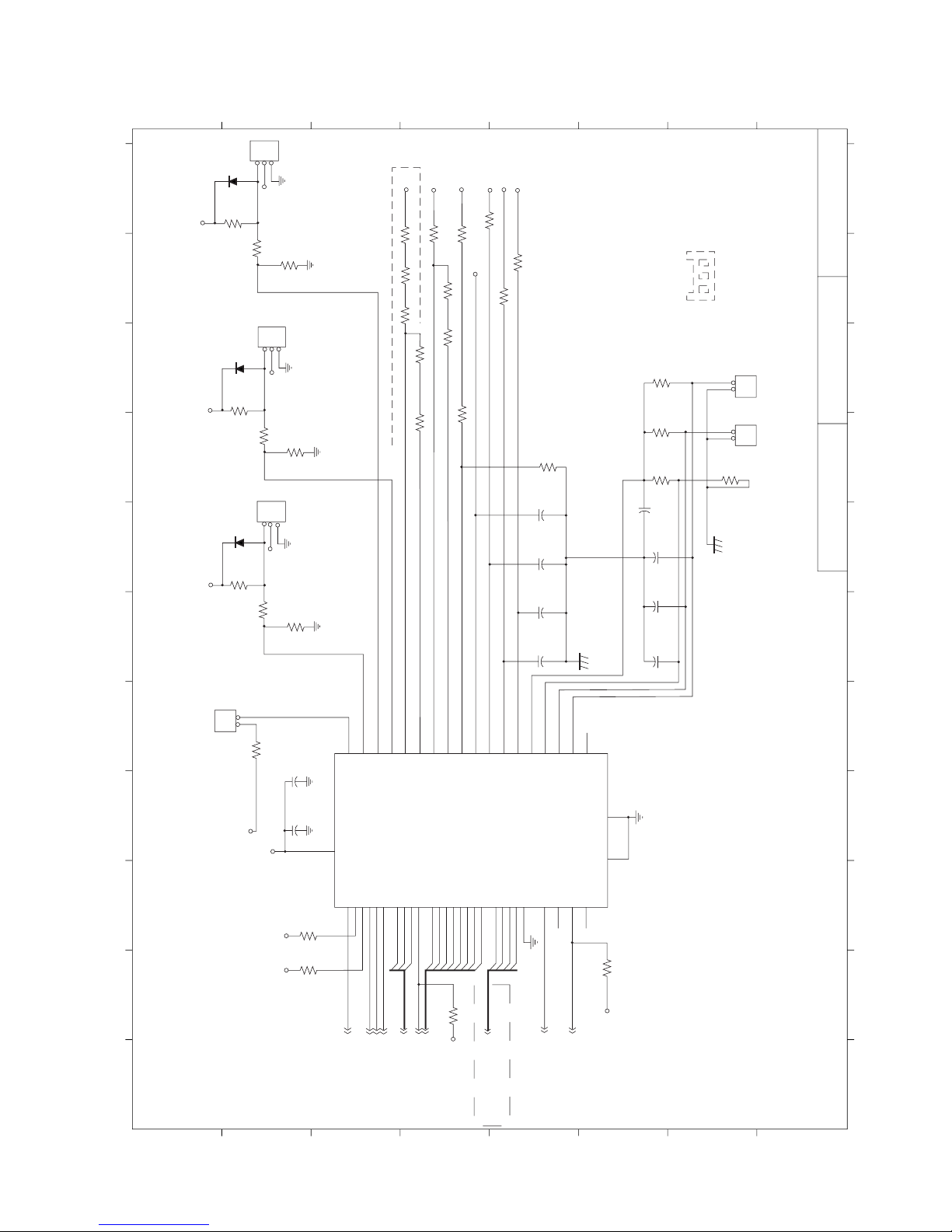
R315
10K
R314
10K
R316
10K
C385
0.1U
C384
0.1U
C387
0.1U
C389
0.1U
C381
0.1U
C350
0.1U
C176
0.1U
R274
10K
R377
R309
10K-NI
8.2K
R378
10K
R310
51K-NI
R311
51K-NI
R312 R313
FAN3x1
D2
1N4148
D5
1N4148
D4
1N4148
R304
10K
R301
10K
R49
4.7K
R45
4.7K
R44
4.7K
CN29
HEADER 2x1
C124
0.1U
C136
10U
R306
4.7K
R305
4.7K
R74
20K
R73
R257
U33
VCC VCC
VCC
VCC
13
3VSB
CPUFAN
-5VD+
-5VD-
-12VD+
-12VD-
+12VD
VCCD
VCC3D
VCORE
VTTD
W83781D
1618192028293130323334363537403938
42
MR
SDA
SCL
CLKIN
IOR-
IOW-A0A1A2CS-D0D1D2D3D4D5D6D7
VID0
VID1
VID2
VID3
VID4
SMI-
RSTOUT-
BEEP/GPO-
IRQ
R290
11 BEEP
6.14 EXTSMI-
1,17 VID[0..3]
4.7K
R152
VCC3
5 PGCS1-
5,7,8,10,14,15,21 SD[0..7]
5,7,8,10,14,15,21 SA[0..2]
16 OSC781
5,7,8,10,14,15,21 IOR-
5,7,8,10,14,15,21 IOW-
5,8 RSTDRV
4.7K
VCC
GNDD
14
27
GNDA
152221
312
CASEOPEN
FAN1 IN/OUT
FAN2 IN/OUT
FAN3 IN/OUT
-5VIN
-5VOUT
-12VIN
-12VOUT
+12VIN
+5VIN
+3.3VIN
VCOREA
VCOREB
VREF
VTIN1
VTIN2
VTIN3
OVT.
4746454811
10
98765
4
4112242517
SA0
SA1
SA2
SD0
SD1
SD2
SD3
SD4
SD5
SD6
SD7
VID0
VID1
VID2
VID3
442326
43
1
2
20K
10M-NI
+12V
+12V
+12V
+12V
+12V
+12V
R302
20K
R303
10K
FAN 3x1FAN 3x1
CN1
CN7
CN26
321
321
321
-5V
-12V
+12V
VCC3
VCCCORE
VTT
20K-NI 20K-NI
R291
210K
R292
20K
R266
R319
R298
10K
10K
10K
VCC
R275
51K
C383
0.1U
12V
G S PU5
SYSTEM
CPU TEMP
CN30
HEADER2x1
CN28
TRJT-1
TC1
TR-1S 10K
1
2
1
2
FAN1
FAN3
FAN2
2
1
3
4
5
6
7
8
2
1
3
4
5
6
7
8
BCDEFGHI JKA
BCDEFGHI JKA
Description: Board No. Drawing No.
SBC8360 18/23SBC8360SYSTEM MONITOR
— 69 —
Page 72

U35
J18
J17
H19
G20
H18
G19
F20
G18
F19
E20
F18
D20
E19
F17
E18
D19
D15
B16
A17
C15
A16
B15
C14
A15
B14
C13
A14
B13
D12
C12
A13
B12
D10
A10
B10
C10
A9
B9
A8
C9
B8
A7
C8
B7
A6
C7
B6
A5
VAA0
VAA5
D18
C19
B20
C18
A20
B19
A19
B18
C17
D16
MC0
MC1
MC2
MC3
MC4
MC5
MC6
MC7
MC8
MC9
MC10
MC11
MC12
MC13
MC14
MC15
MB0
MB1
MB2
MB3
MB4
MB5
MB6
MB7
MB8
MB9
MB10
MB11
MB12
MB13
MB14
MB15
MA0
MA1
MA2
MA3
MA4
MA5
MA6
MA7
MA8
MA9
MA10
MA11
MA12
MA13
MA14
MA15
AA0
AA1
AA2
AA3
AA4
AA5
AA6
AA7
AA8
AA9
U2
T3
R4
T2
U1
R3
T1
R2
R1
P2
N3
P1
N2
M4
M3
N1
J1
J2
H1
J3
J4
H2
G1
H3
G3
F2
E1
F3
D1
E2
F4
E3
W6
V7
Y6
W7
V8
Y7
W8
U9
V9
Y8
W9
Y9
V10
W10
Y10
U10
U11
Y11
W11
V11
Y12
Y13
V12
U12
W13
Y14
V13
W14
Y15
V14
W15
Y16
V15
Y17
W16
U15
P35
P34
P33
P32
P31
P30
P29
P28
P27
P26
P25
P24
P23
P22
P21
P20
P19
P18
P17
P16
P15
P14
P13
P12
P11
P10
P9
P8
P7
P6
P5
P4
P3
P2
P1
P0
GD31
GD30
GD29
GD28
GD27
GD26
GD25
GD24
GD23
GD22
GD21
GD20
GD19
GD18
GD17
GD16
GD15
GD14
GD13
GD12
GD11
GD10
GD9
GD8
GD7
GD6
GD5
GD4
GD3
GD2
GD1
GD0
AD0
AD1
AD2
AD3
AD4
AD5
AD6
AD7
AD8
AD9
AD10
AD11
AD12
AD13
AD14
AD15
AD16
AD17
AD18
AD19
AD20
AD21
AD22
AD23
AD24
AD25
AD26
AD27
AD28
AD29
AD30
AD31
P0
P1
P2
P3
P4
P5
P6
P7
P8
P9
P10
P11
P12
P13
P14
P15
P16
P17
P18
P19
P20
P21
P22
P23
P24
P25
P26
P27
P28
P29
P30
P31
P32
P33
P34
P35
MD0
MD1
MD2
MD3
MD4
MD5
MD6
MD7
MD8
MD9
MD10
MD11
MD12
MD13
MD14
MD15
M 20
ENABKL 20
SHFCLK 20
FLM 20
ENAVDO 20
LP 20
ENAVEE 20
R2
560
AVSS1
AVSS1 20
DDDA 20
DDCK 20
RED 20
GREEN 20
BLUE 20
HSYNC 20
VSYNC 20
CT69030
P[0..35] 20
R140
VAA5
VAA0
R139
4.7K
4.7K
C3
VCC3
VCCVP
VCCVA
VCC3
VCC3
VCC3
5.14.15.22 PIRQA-
3.14 GPAR
3.14 GDEVSEL-
3.14 GSTOP-
3.14 GFRAME-
3.14 GTRDY-
3.14 GIRDY-
3 -GBE0
3 -GBE1
3 -GBE2
3 -GBE3
3 GCLKO
3.5.12.15.21.22 PCIRST-
3 GD[D..31]
R87
4.7K
R90
4.7K
R138
4.7K
AVSS1
20 AVSS1
VCCVS
GNDVP
GNDVS
L11
VCC3
VCC3
VCC3
BEAD
BEAD
BEAD
L10 C121
1U
C120
0.1U
C77
0.1U
C82
1U
L5
BEAD
BEAD
L14
L12
C123
0.1U
C122
1U
RCLK/EXTMCLK
SGCLKI
SGCLKO
MVCC
MVCC
MVCC
CVCC
VVCC
IVCC
IVCC
PVCC
PVCC
DVCC
SVCC
AVCC
BVCC
BVCC
AGND
RGND
SGND
PGND
PGND
GND
GND
GND
GND
GND
GND
GND
GND
INT#
PAR
DEVSEL
SERR
PERR
STOP
FRAME
TRDY
IRDY
C/BE-0
C/BE-1
C/BE-2
C/BE-3
IDSEL
STBY
BCLK
RST
16 OSCVGA
E17
C20
H17
N17
D13
W1
U13
D9
W12
D5C4U8B3U5N4H4
Y2
Y1A2A3
B4
D14
P17
G17
U7
P4
G4
D7
U14
A4
M1
L4L3L2
L1
K2K4K1
P3M2K3
F1
G2
E4
D2
C1
-GSERR
-GPERR
GD25
STBY
DQMAH/CASAH
DQMAL/CASAL
RAS0
SWE/WEA
DQMBH/CASBH
DQMBL/CASBL
SCAS/WEB
DQMCH/CASCH
DQMCL/CASCL
RAS1
AA10/WEC
DQMDH/CASDH
DQMDL/CASDL
SCKE/WED
VCLK
HREF
PCLK
VREF
VRDY
M/DE/BLANK
ENABKL
SHCLK
FLM
ENAVOD
LP/DE
ENAVEE
RSET
GPIO2/DDDA
GPIO3/DDCK
RED
GRN
BLUE
HSYNC
VSYNC
Y3V4W3U3V2V1T4
C6
Y18
W17
V17
V16
U16V6U6Y5W5V5Y4W4W2V3U4
A11
D11
C11
B11
B17
C16
A18
J19
H20
K18
J20
R19
P18
T20
R18
U20
T19
R17
T18
U19
V20
T17
U18
V19
W20
W19
U17
V18
Y19
W18
R20
P19
N18
P20
N19
M17
M18
N20
M19
M20
L18
L19
L20
L17
K17
K20
GP0/ACTI
GP1/32KHZ
ROMEN/MCLKOUT
VP0
VP1
VP2
VP3
VP4
VP5
VP6
VP7
VP8
VP9
VP10
VP11
VP12
VP13
VP14
VP15
2
1
3
4
5
6
7
8
2
1
3
4
5
6
7
8
BCDEFGHI JKA
BCDEFGHI JKA
Description: Board No. Drawing No.
SBC8360 19/23SBC8360CT69030
— 70 —
Page 73

VCCM
CN11
1357911131517192123252729313335373941
43
135791113
15
C79
180P
C112
180P
AVSS1
C148
180P
C137
180P
246
8
101214
16
1357911131517
19
246
8
1012141618
20
S1G1S2
G2
U17
SI9953-P
2N3904Q42N3904
Q3
R1
+12V
51K
R48
51K
R76
4.7K
R82
ENABKL
19 ENAVDD
4.7K
D1D1D2
D2
876
5
123
4
246
8
1012141618202224262830323436384042
44
+12VM
-12V
P1 19
P3 19
P5 19
P7 19
P9 19
P11 19
P13 19
P15 19
P17 19
P19 19
P21 19
P23 19
FLM 19
LP 19
ENABKL 19
19 ENAVEE
19 P0
19 P2
19 P4
19 P6
19 P8
19 P10
19 P12
19 P14
19 P16
19 P18
19 P20
19 P22
19 M
19 P24
19 P26
19 P28
19 P30
19 P32
19 P34
P25 19
P27 19
P29 19 P31 19
P33 19
P35 19
19 SHFCLK
HEADER 8X2H
R-1
G-2
B-3
CN22
AVSS1
AVSS1
AVSS1
HS-13
VS-14
AVSS1
DDCDAT
DDCDAT
L6R396
R401
R400
R399
33
33
33
BEAD
L16
L13L9BEAD
BEAD
BEAD
DDCCLK
VS-14
HS-13
DDCCLK
HEADER 22X2H 2.0
U0504D
74HCT14
GND
CN6
HEADER 10X2H 2.0
+12VM
+12VM
+12VM
C1 C62
0.1U
C4
0.1U
C69
47U/10V
JP9
HEADER 3X1
C80
27P
C93
27P
C74
27P
C60
0.1U
C81
27P
C90
27P
C75
27P
L4
BEAD
L8
L7
BEAD
R94
75
R83
75
L53
R397
R402
19 RED
19 GREEN
19 BLUE
19 VSYNC
19 HSYNC
19 DDDA
19 DDCK
000
R398
BEAD
R86
75
+12V
C68
3.3U/25V
C59
0.1U
C58
0.1U
VCCM
VCCM
VCCM
DVCC
VCC
BEAD
BEAD
AVSS1
L15
G-2
B-3
R-1
3.3U/25V-NI
GND
GND
AVSS1
19 AVSS1
VCC3 VCC
3
2
1
DVCC
GND
GND
VCCM
+12VM
VCCM
+12VM
98
33
2
1
3
4
5
6
7
8
2
1
3
4
5
6
7
8
BCDEFGHI JKA
BCDEFGHI JKA
Description: Board No. Drawing No.
SBC8360 20/23SBC8360
CRT AND LCD CONNECTORS
— 71 —
Page 74

VCC
U32
74F174
346
111314
HAND
SA0
SD3
SD2
SD1
SD0
VCC
21
001
1
010
1
111
1
111
1
111
1
000
0
000
0
001
1
010
1
D0000-01FFF
D2000-03FFF
D4000-05FFF
D5000-07FFF
20 19 18 17 16 15 14 13
JP2
HEADER 2X2
U12
5 PGCS0-
20V8 DIP20
R308
BKLENA
PGCS0-
IOW- 5,7,8,10,14,15,18
5,7,8,10,14,15,18 IOR-
5,7,8,10,14,15,18 SA[0..14]
U13
DOCCSJ
SD0
SD1
3
6
8
11
14
SD2
SD3
U29
B1
B2
B3
B4
A1
A2
GA1#
GA2#
A3
A4
GA3#
GA4#
DID0
DID1
DID2
DID3
74F125
VCC
VCC
251491210
13
R307
10K
DIORDJ
VCC
SD0
SD1
SD2
SD3
D1D2D3D4D5D6CLK
CLR
Q1Q2Q3Q4Q5
Q6
DOD1
DOD3
DID0
DID2
13579
246
8
10
346
111314
9
1
2571012
15
DOD0
DOD1
DOD2
DOD3
3,5,12,15,19,22 PCIRST-
U11
74F174
CN24
HEADER 5X2H
DIOWRJ
PCIRST-
DOD0
DOD2
DID1
DID3
VCC
DOC/SRAM
DIO CONN
VCC
VCC
DOD0
R264
4.7K
R261
R263
R262
4.7K
4.7K
4.7K
R299
4.7K
R284
R300
R295
4.7K
4.7K
4.7K
DOD1
DOD2
DOD3
DID0
GND
DID1
DID2
DID3
VPP
SOCKET-DIP32
SD[0..7] 5,7,8,10,14,15,18
1
5,14,15 SMEMW-
5,14,15 SMEMR-
R322
4.7K
R379
4.7K
4.7K
R321
4.7K
VCC
S2
S1
123456789
1011131423
SA14
SA13
SA12
SA11
SA10
SA9
SA8
SA7
SA6
SA5
SA4
SA3
SA2
SA1
SA0
A16
A15
A14
A13
A12
A11
A10A9A8A7A6A5A4A3A2A1A0
DQ7
DQ6
DQ5
DQ4
DQ3
DQ2
DQ1
DQ0
21201918171514
13
SD7
SD6
SD5
SD4
SD3
SD2
SD1
SD0
2
3
29
284252326
27
56789
10111231242230
WE#
OE#
CE#
PWD#
15161718192021
22
DOCCSJ
DIOWRJ
DIORDJ
BKLENA
WDTTR
SA14
SA13
SA0
SA1
SA2
5,14,15 SA19
5,14,15 SA18
5,7,14,15 SA17
5,7,14,15 SA16
5,7,8,14,15 SA15
I0I1I2I3I4I5I6I7I8I9I10
I11
I12
I13
F0F1F2F3F4F5F6
F7
1
3
2
4
9
1
CLK
CLR
D1D2D3D4D5
D6
123456789
RA2
RA3
RTCC
RST
GND
RB0
RB1
RB2
RB3
RA1
RA0
CLKI
CLKO
VCC
RB7
RB6
RB5
RB4
181716151413121110
123
Q1Q2Q3Q4Q5
Q6
2571012
15
HANDSK
COMD1
PICD3
PICD2
PICD1
PICD0
WDTTR
VCC
R317
4.7K
C386
0.1U
R318
4.7K
U15
PIC16C54
R410
1501%
5,14,15 IOCHK-
WDT OUT
11 WDTRST
HEADER 3X1
JP7
OSCPIC 16
VCC
VCC
R287
4.7K
VCC
VCC3
2
1
3
4
5
6
7
8
2
1
3
4
5
6
7
8
BCDEFGHI JKA
BCDEFGHI JKA
Description: Board No. Drawing No.
SBC8360 21/23SBC8360DIO, DOC AND WDT
— 72 —
Page 75

VCC
11 WAKEUP
LANVDD
RTL8139B
MD5
MD6
MD7
LED0
LED1
LED2
VDD
CEXT4
CEXT3
GND
TXD+
TXD-
VDD
CEXT2
CEXT1
RXIN+
RXIN-
RTSET
GND
RTT1
RTT2
RTT3
GND
XTAL50
REXTPHY
VDD
LFTS
LFTM
GND
VDD
VDD
GND
MA16
MA15
MA14
MA13
MA12
MA11
102
101
100
99
98
97
96
95
94
93
92
91
90
89
88
87
86
85
84
83
82
81
80
79
78
77
76
75
74
73
72
71
70
69
68
67
66
65
103
104
105
106
107
108
109
110
111
112
113
114
115
116
117
118
119
120
121
122
123
124
125
126
127
128
AD31
AD30
AD29
AD28
AD27
AD26
AD25
AD24
3,4,15,19 PIRQA-
5,19,21 PCIRST-
16 LANPCLK
3,14 PGNT4-
3,14 PREQ4-
LANVDD
3,5,12,15 CBE3-
3,5,12,15 CBE2-
3,5,12,14,15 FRAME-
3,5,12,14,15 IRDY-
3,5,12,14,15 TRDY-
3,5,12,14,15 DEVSEL-
3,5,12,14,15 STOP-
AD6
AD7
AD8
AD9
AD10
AD11
AD12
AD13
AD14
AD15
AD16
AD17
AD18
AD19
AD20
AD21
AD22
AD23
AD24
VDD
CBE3B
IDSEL
AD23
AD22
AD21
GND
AD20
AD19
AD18
AD17
VDD
AD16
CBE2B
FRAMEB
IRDYB
TRDYB
GND
DEVSELB
STOPB
PERRB
SERRB
PAR
CBE1B
VDD
AD15
AD14
AD13
AD12
GND
AD11
AD10
AD9
AD8
VDD
CBE0B
AD7
AD6
1
2
3
4
5
6
7
8
9
10
11
12
13
14
15
16
17
18
19
20
21
22
23
24
25
26
27
28
29
30
31
32
33
34
35
36
37
38
MD4
MD3
MD2
VDD
MD1
MD0
VDD
ROMCSB
GND
GND
GND
INTAB
RSTB
CLK
GNTB
REQB
VDD
AD31
AD30
AD29
AD28
GND
AD27
AD26
AD25
AD24
LANVDD
R269
330
R210
10K
R211
R226
R221
1K
1.8K 1%
10K
R270
330
LANVDD
Q10
LT1117
5VSB
L45
123
4
1
2
4
3
BEAD
JP17
HEADER 4X1
5VSB 5VSB
CBE0- 3,5,12,15
CBE1- 3,5,12,15
PAR 3,5,12,15
SERR- 3,5,14,15
PERR- 14,15
RTL8139
AD[0..31] 3,5,12,15
LANVDD
LANVDD
U8
L47
AVCC2
L22
AVDD
L46
C217
27P
Y4
25MHZ
R329
49.9
C405
27P
R324
49.9
R296
49.9
L41
L42
L43
L44
BEAD
U16
LF8275
BEAD
BEAD
BEAD
RJ-1
RJ-2
TRX+
TRX-
TTX-
TTX+
R297
49.9
C380
0.1U
C403
27P
C391
0.1U
R325
75
R323
75
C394
0.01U/1KV
C392
0.1U
R326
75
R320
75
TXD+
RXIN+
RXIN-
TXD-
132
11
10
9
16151467
8
RD+
RD-CTTD-CTTD+
RX+
CT
RX-
TX-
CMT
TX+
R404
33
R403
33
C213
27P
R406
1.8K 1%
R407
0
AVDD
AVDD
AVDD
BEAD
BEAD
L
GND5
GND4
GND3
GND2
GND1
LANVDD
EECS
R408
0
R409
L20
BEAD
5VSB
NC
NC
LANVDD
U28
93C46
RMA2
RMA1
RMA0
123
4
CSCKDI
DO
VCC
NC
NC
GND
GND1
GND2
GND3
GND4
GND5
876
5
CN25
HEADER 4x2H
13579
TTX+
TRX+
RJ-2
RJ-1
TTX-
RJ-2
TRX-
246
8
10
R405
10K
MA10
MA9
GND
MA8
MA7
VDD
VDD
MA6
GND
GND
PCITSTB
MA5
MA4
MA3
EECS
MA2
MA1
MA0
VDD
AD0
AD1
AD2
AD3
AD4
GND
AD5
64636261605958575655545352515049484746454443424140
39
RMA2
RMA1
RMA0
AD0
AD1
AD2
AD3
AD4
AD5
LANVDD
LANVDD
LANVDD
C277
1U
C268
1U
C278
0.1U
C279
1U
8139B:
8139C:
ON: L45,L46,L47,R407
MAKE_OM_LAN:
R41,R43 ON
OSC=50MH3:
ORY=25MH2
R125 OFF
R125 ON
ON: Q10,R406,R226
OFF: Q10,R406
OFF: L45,L46,L47,L22,
R407, R221
C328
0.1U
C282
0.1U
C326
0.1U
C222
0.1U
C252
0.1U
C243
0.1U
C224
0.1U
LANVDD LANVDD
AVDD
BEAD
L23
AVDD LANVDD LANVDD LANVDD LANVDD LANVDD
2
1
3
4
5
6
7
8
2
1
3
4
5
6
7
8
BCDEFGHI JKA
BCDEFGHI JKA
Description: Board No. Drawing No.
SBC8360 22/23SBC8360LAN
— 73 —
Page 76

VCCCORE
VCCCORE
VTT
VTT
VCC3
VCC3
VCC3 VCC3
VCC3
VCC3
VCC3
VCC3
VCC3
VCC
VCC
VCC 5VSB
+12V -12V
C299
1U
C39
0.1U
C3
0.1U
C218
0.1U
C290
0.1U
C367
0.1U
C266
0.1U
C323
0.1U
C339
0.1U
C318
0.1U
C324
0.1U
C341
0.1U
C390
0.1U
C234
0.1U
C361
0.1U
C360
0.1U
C274
0.1U
C404
0.1U
C151
0.1U
C86
0.1U
C85
0.1U
C108
0.1U
C99
0.1U
C101
0.1U
C135
0.1U
C119
0.1U
C88
0.1U
C154
0.1U
C84
0.1U
C109
0.1U
C118
0.1U
C97
0.1U
C76
0.1U
C70
0.1U
C2
1000U
C35
1000U
C411
1U
C280
1U
C388
1U
C161
0.1U
C160
0.1U
C159
1U
C407
1U
C167
0.1U
C166
0.1U
C172
0.1U
C128
0.1U
C139
0.1U
C89
0.1U
C83
0.1U
C96
0.1U
C153
0.1U
C152
0.1U
C150
0.1U
C170
0.1U
C163
0.1U
C146
0.1U
C343
1U
C42
1U
C40
1U
C38
1U
C41
1U
C43
1U
C44
1U
C396
1U
C399
1U
C398
1U
C397
1U
C269
1U
FOR CPU
C238
1U
C168
0.1U
C145
0.1U
C73
1U
C216
1U
C149
0.1U
C162
0.1U
C408
1U
C178
1U
C295
1U
C284
1U
C317
1U
C47
1U
C296
1U
C37
1U
C36
1U
C336
1U
C375
1U
C329
1U
C363
1U
C225
1U
C227
1U
C303
1U
C226
1U
C346
1U
C335
1U
C250
1U
C262
1U
C285
1U
C316
1U
C302
1U
C315
1U
C327
1U
C294
1U
C298
1U
C313
1U
C333
1U
C356
1U
C374
1U
C430
1U
C431
1U
C71
10U
C67
10U
C413
10U
C66
1U
C126
1U
C165
0.1U
C116
0.1U
C211
0.1U
C210
0.1U
C127
0.1U
C125
0.1U
C111
0.1U
C421
1U
C422
1U
C409
1U
C65
1U
C230
1U
C115
0.1U
C106
0.1U
C104
0.1U
C103
0.1U
C102
0.1U
C191
0.1U
C140
0.1U
C155
0.1U
C156
0.1U
C157
0.1U
C131
0.1U
C5
0.1U
C194
0.1U
C382
1U
C358
1U
C78
3.3U/25V
C95
3.3U/25V
C110
1U
C393
0.1U
C406
0.1U
C63
0.1U
C372
0.1U
C325
0.1U
C301
0.1U
C232
0.1U
C64
1U
2
1
3
4
5
6
7
8
2
1
3
4
5
6
7
8
BCDEFGHI JKA
BCDEFGHI JKA
Description: Board No. Drawing No.
SBC8360 23/23SBC8360
— 74 —
Page 77

MOUSE
PS/2 and K/B
AU-DATA
KB-GNDL2
INDUCTOR
C8
22P
C6
22P
C7
22P
KV1KB-VCC
AU-CLK
PS2-6
12345
6
PS&KB
KB-VCC
KB-CLK
AU-DATA
KB-GND
KB-GND
KB-DATA
KB-GND
KB-VCC
AU-CLK
VCC
JP2X5A
13579
246
8
10
USB
USB
USBVCC
UV0-
UV0+
USBVCC
UV1-
UV1+
HEADER 4X2A
123
4
567
8
CN1
JP2X5A
13579
246
8
10
KB
KB-DATA
KB-GNDL1
INDUCTOR
L3
INDUCTOR
C5
22P
C3
22P
C4
22P
KV2KB-VCC
KB-CLK
PS2-6
12345
6
UV0-
UV0+
USBVCC
UV1-
UV1+
C9
0.1U
FDD CN
FDDA
DSKCHG-
SIDE1-
RDATA-
WPT-
TRK0-
WGATE-
WDATA-
STEP-
DIR-
DRVS0-
MOTE0-
INDEX-
REDWC-
JP2X17A
33312927252321191715131197531
34323028262422201816141210
864
2
FDD
SCSI26
26252423222120191817161514
131211
10
987654321
DSKCHG-
MOTE0-
DIR-
STEP-
WGATE-
TRK0-
WPT-
F1
FUSE
VCC
FDDDVCC
INDEX-
DRVS0-
REDWC-
WDATA-
RDATA-
SIDE1-
C2
10U/6V
FDDDVCC
C1
0.1U
2
1
3
4
5
6
7
8
2
1
3
4
5
6
7
8
BCDEFGHI JKA
BCDEFGHI JKA
Description: Board No. Drawing No.
PANEL 2120PANEL
PS/2 AND K/B, USB, FDD CN
— 75 —
Page 78

10. PARTS LIST
PARTS LIST
MODEL : QT-7300 (EX-963)
CONTENTS
EXPLODE VIEW............................................................................................................................ 77
1. MAIN COMPONENTS .............................................................................................................78
2. FDD/MOUSE/KB PCB ............................................................................................................. 79
3. LCD UR PCB ........................................................................................................................... 79
4. MULTI I/O PCB........................................................................................................................ 79
5. TOUCH PANEL CONTROL PCB ............................................................................................ 80
6. DRAWER DRIVE PCB ............................................................................................................80
7. RELAY PCB............................................................................................................................. 80
8. LCD CONVERTOR PCB ......................................................................................................... 80
9. OTHERS.................................................................................................................................. 81
10. DRAWER................................................................................................................................. 82
DL-2773 (M Type).................................................................................................................... 82
DL-2915 (M Type).................................................................................................................... 84
DL-3615 (L Type)..................................................................................................................... 86
11. DRAWING ............................................................................................................................... 88
NOTES :
1. Price and specifications are subject to change withput prior notice.
2. As for spare parts order and supply, refer to the “GUIDEBOOK for Spare Parts Supply”, published
separately.
3. The numbers in item column corespond to the same numbers in drawing.
4. CASIO does not supply the spare parts without parts code.
5. Remarks
Q'ty : Quantity used per unit
RANK: A = Essential
B = Stock recommended
C = Less recommended
X = No stock recommended
— 76 —
Page 79

23
3
21
33
15
29
20
22
4
16
14
12
13
2
18
32
33
25
27
28
1
9
19
40
11
26
10
30
31
39
34
39
5
5
7
17
6
8
40
— 77 —
40
36
41
35
38
37
43
42
Page 80

PARTS PRICE LIST
QT-7300
N
Item
Code No.
Parts Name
Specification
Q
Price Code
R
1. Main components
N 1 9487 0558
/with LED COVER
2
9487 0529
COVER/REAR
EDM-2314 (380/CASIO)
00-41500955
1DEX31904 9027
CAP/DUST SPILL
6332000010 (345)
00-41500970
1AMX
(EX960AC) (50)
5
1904 9044
LCD SET PIECE
EAM-1420
00-11100215
4ACX69487 0617
LCD-STAND-RSL
EBM-1565
00-33900305
1BLX79487 0618
LCD-STAND-LSF
EBM-2394
00-33900400
1BKX
8
9487 0619
BASE/METAL
EBM-2395
00-25400300
1CTX91904 9077
PLATE/SLOT
EBM-1381
00-10100785
1AQX
10
9487 0745
PANEL/CONNECTOR
ECM-1405B
00-40500306B
1
BF
X111904 9032
COVER/SLOT
EAM-1001 (T)
00-46501110
1ADX
12
9487 0533
BRACKET/KEYBOARD FDD
EBM-2126
00-41501980
1ATX131904 9029
STAND/FAN
EBM-1384
00-40500305
1AKX
14
9487 0550
SEPARATOR/ALUMI
EBM-2252
00-40504420
1AZX151904 9022
PLATE/LCD-REINFORCE
ECM-1411
00-10101250
1BKX161904 9063
PANEL/TOUCH
N010-0550-T711
00-12900030
1EAA179487 0620
LCD
AA121SJ02
00-12900221
1EUA
(DC12V0.9W)
19
9487 0763
SUPPLY/POWER
VLT100-4000
00-20105025
1EGA
20
9487 0670
MOTHER BOARD
SBC8360VE-4M(B1)
00-05100510B1
1FFA
CONNECTOR
22
9487 0746
HDD
MHR2010AT
00-60702500
1EMC
23
9487 0532
CABLE/HDD
EAH-0433
00-47418261
1BMC
LED CABLE
9487 0524
HARNESS ASSY
EAH-0434
00-47418262
1AEC
PS CABLE
9487 0523
HARNESS ASSY
EAH-0432B
00-47418260
1BRC
(22X14X10t)
4Q
N
FRONT COVER
EDM-2313 (380/CASIO) 00-41500935 1 CP C
4 1904 9070 RUBBER/WATERPROOF
N
1904 9030 PLATE/41P-PRESS EAM-1386 00-10100784 1 AE X
N
N
9487 0621 INVERTER/CFL CXA-L0612A-VJL 00-02802040 1 CZ C
N 9487 0534 HARNESS ASSY EAH-0239C (T) 00-47416475C 1 AG C
1904 8980 HARNESS ASSY EAH-0120A (T) 00-47415100 1 AF C
N 9487 0535 HARNESS ASSY EAH-0119B (T) 00-47415090B 1 AC C
N 9487 0536 HARNESS ASSY EAH-0118B (T) 00-47415080B 1 AC C
1904 9004 HARNESS ASSY EAH-0114 (T) 00-47413365 1 AV C
N 9487 0563 CABLE ASSY/LCD 050009-02 20-050009-02 1 CY C
18 1904 8977 FAN
N
N
1904 9008 HARNESS ASSY EAH-0113 (T) 00-47413364 1 AO C
N 21 9487 0525 CARD/RISER
N
N
N
N
1906 9292 CLAMP/FERRITE ZCAT1518-0730 00-21002000 1 AV C
CLIP S-508 00-40200030 4 X
N 9487 0528 COOLER/CPU CM21 00-00500086 1 CT B
9487 0215 CORE/FERRITE
N 9487 0671 CPU
N 9487 0539 CUSHION EAM-1450B (3X12X54) 00-60200580 1 AB X
N 9487 0641 DIMM/64MB HSD-B DN128B 00-03800210 1 DX A
N 9487 0537 DUCT/FAN 7262003007 00-41501376 1 BL C
1904 9055 HARNESS ASSY EAH-0115(T) 00-47413366 1 AT C
1904 9066 HARNESS ASSY EAH-0107 (T) 00-47413361 1 AM C
9487 0217 HARNESS ASSY EAH-0151 (T) 00-47416120 1 AB C
N 9487 0562 HARNESS ASSY EAH-0448 (T) 00-47418291 1 CR C
9487 0206 HOLDER/CARD 6337000001 00-41501420 1 AM C
INLET/AC JR-101S (U420) 00-20300510 1 X
LABEL/RATING 00-00000495 1 X
N 9487 0541 MYLAR/PC-B EAM-1783 00-13100030 1 AY X
N 9487 0542 PARTITION QT7000/7100 00-22410602 2 AF X
N 9487 0564 PLATE/INSULATION EAM-2253 00-41500995 1 AY C
RIVET CR-HT52 KASAMI 00-60600200 1 X
N 9487 0559 SCREW 3X12 BLACK 00-55100193 12 AA X
1904 9035 SCREW S 3X6 (NI) 00-55100530 3 AA X
6322000000
KD1204PKB-2
RISER W/O ISA
T5 T-221013
RB80526RY850128SL5
00-12301080 1 BO X
00-00501423 1 CE C
00-05100033 1 CR C
00-40300110 1 AD C
00-00500160 1 EG A
-78-
Page 81

N
Item
Code No.
Parts Name
Specification
Q
Price Code
R
N 9487 0560 SCREW S 3X6 BLACK 00-55100529 21 AA X
2. FDD/Mouse/KB PCB
(24)
PCB/PANEL 2000(T)
EBL-0453 (1)
00-00402040
1
X
C1,12,14
CHIP/CC
MCH182FN104ZK
00-01104014
3
X
C2,11,13
CHIP/TANTAL
TCFGBIC106M8R
00-01400320
3
X
C3-8
CHIP/CC
MCH185A220JK
00-01104044
6
X
CN1,PS&KB
1904 8947
CONNECTOR
5X2(FEMALE)180
00-03200830
2ADC
F1
9487 0552
SWITCH/POLY
RXE110 60V 1.10A
00-20203015
1ANC
F2,3
9487 0553
SWITCH/POLY
MINI SMDC100
00-20204008
2AIC
FDD
9487 0554
CONNECTOR
SCS126
00-03204180
1CCC
FDDA
1904 8946
CONNECTOR
17X2(FEMALE)
00-03200820
1AHC
JP1
1904 8926
CONNECTOR
S2B-XH-A
00-04001260
1ABC
K/B,MOUSE
9487 0556
CONNECTOR
MIN-DIN 6P
00-03200810
2AMC
L1-3
INDUCTOR/CHIP
SBY321611T-320Y-S
00-62100310
6
X
L1-5
INDUCTOR/CHIP
FB2012
00-01801450
5
X
USB
9487 0555
CONNECTOR
USB CONN TYPE A
KEYBOARD MOUSE
3. LCD VR PCB
(25)
PCB/PANEL 2000-6 (T)
EBL-0453 (2)
00-00402060
1
X
(GREEN 3PAI )
CN1
9487 0213
CONNECTOR
DF3D-5P-2H (21)
00-03202091
1AJC
CN2
1904 8963
CONNECTOR
DF3-4P-2H (21)
00-03202080
1AIC
CN3
1904 8964
CONNECTOR
DF3-2P-2H (21)
00-03202070
1AHC
R2.9
1904 8961
RESISTOR/CHIP
MCR10EZHJ000
00-01610010
2AAX
VR1
1904 8965
VR
VR B10K
00-03100510
1ALB
4. Multi I/O PCB
(26)
PCB/MULTI I/O(T)
EBL-0453 (3) REV;A2
00-00402050
1
X
C1-32
CHIP/CC
MCH185A101JK
00-01104049
32
X
DB9P(MALE)
COM1B.3B
1904 8958
CONNECTOR
5X2 (MALE)
00-03200890
2AAC
D101
NET
1904 8952
CONNECTOR
RJ45 (QT7000)
00-03200840
1ALC
NETA
1904 8953
CONNECTOR
4X2 (FEMALE)
00-03200850
1ADC
PRN DB25P(x2)
9487 0517
CONNECTOR
DB25-SK-2-4-4#40
00-03204000
1APC
PRNA
1904 8956
CONNECTOR
13X2 (FEMALE)
00-03200870
1AFC
COM1A-4A
1904 9036 SCREW B3X5 00-55100671 36 AA X
1904 9037 SCREW 4X6 00-55101045 4 AA X
1904 9038 SCREW 3X25 00-55100535 4 AA X
1904 9080 SCREW S3X4(NI) 00-55101206 3 AA X
1906 0855 SCREW P2X6 00-55100030 2 AA X
1904 9041 SCREW P3X6SW 00-55100120 5 AA X
N 9487 0561 SCREW EAM-2302 00-41502100 4 AB X
1904 9042 SCREW 3X4 00-55100775 7 AA X
SHEET/INSULATION EAM-1449 00-13101240 1 X
SHIELD/SHRINK 30X100M L-170mm 00-55700351 1 X
N 9487 0538 SWITCH ASSY/POWER 030426-00c 20-030426-00C 1 CG C
1904 8972 SWITCH/POWER SJ-W2H4A-03BB2 00-20200115 1 AU C
TIE/I TR-30R 00-40300230 3 X
TIE/INSULOCK CV-075 00-40300500 1 X
TUBE/HS (T) 5PAI L-20MM 00-55700610 4 X
TUBE/SUMI 25PAI L-165 00-55700115 1 X
1904 9043 WASHER 8X0.8(3MM) 00-55300110 3 AA X
1904 9081 WASHER/GEAR M3 00-55400020 1 AA X
N
N
N
N
N
N 9487 0551
BOARD ASSY/FDD USB
010657-01 00-69900270 1 CR C
00-03204190 1 AH C
PCB/FDD EAL-0607 00-00402380 1 X
1904 8960 LED
SLR-342MG
00-02700220 1 AB B
N RESISTOR/CHIP MCR10EZHJ562 00-01610269 1 X
N RESISTOR/CHIP MCR03EZHJ000 00-01612001 2 X
COM1-4,
N
9487 0516 CONNECTOR DE09-PK-2-4-4#40 00-03203840 3 AK C
N
PS&KB
1904 8947 CONNECTOR 5X2(FEMALE) 00-03200830 6 AD C
-79-
Page 82

N
Item
Code No.
Parts Name
Specification
Q
Price Code
RNVGA DB15P(x2)
9487 0518
CONNECTOR
HD15-SE-A
00-03204100
1ANC
VGAA
1904 8955
CONNECTOR
8X2 (FEMALE)
00-03200860
1AEC
1904 8957 HEADER 3PX2 00-04005030 4 AA X
5. Touch Panle Ccontrol PCB
(27)
PCB/TSCC(T)
EBL-0453 (4)
00-00402010
1
X
C10
CHIP/CC
MCH185C681KK
00-01104580
1
X
C11
CHIP/CC
MCH185C472KK
00-01104370
1
X
8. 20-24
C4.5.13.16.17.1
C6-9
CHIP/CC
MCH185C222KK
00-01104120
4
X
CN2
1904 8926
CONNECTOR
S2B-XH-A
00-04001260
1ABC
CN3
1904 8927
CONNECTOR
53015-1710
00-04003048
1ADC
D3-9
1904 8924
DIODE/DUAL
DAN217T146
00-00801320
7ABB
Q1.3
1904 8922
TRANSISTOR
DTC114TKAT146
00-00700885
2BKB
Q2.4.5
1904 8923
TRANSISTOR/DIGITAL
DTA124EKAT146
00-00700877
3AAB
. 14
R17
CHIP/CC
MCR03EZHJ822
00-01612810
1
X
R19.20.23.24
CHIP/CC
MCR03EZHJ101
00-01612008
4
X
18
R6
CHIP/CC
MCR03EZHJ203
00-01612202
1
X
22
U1
1904 8919
LSI
N010-0559-V021
00-12900035
1CIAU21904 8920
CPU
HIN232CB (T)
00-00501390
1BAAU31904 8921
EEP-ROM
S-29390AFJA-TB
00-00521010
1BKAY11904 8925
OSCILLATOR/CERAMIC
CSTCS8.00MT-TC
00-02300080
1AKX
6. Drawer drive PCB
(28)
PCB/CDCC(T)
EBL-0453 (5) Rev.A2
00-00402030
1
X
25,27,26,28,24
9487 0520
PCB ASSY SET (4pcs)
20-010159-07
1DWC
C1,3
CHIP/CC
MCH215F104ZK
00-01103120
2
X
C2,4
CHIP/CC
MCH185C102KK
00-01104050
2
XC5CAP/E
100 MF25V
00-01200907
1
XC6CHIP/CC
MCH185C561KK
00-01104410
1
XC8CAP/E
4700 MF 35V
00-01200420
1
X
CN1
1904 8939
CONNECTOR
TM2REA-1212
00-03202020
1BKC
D1,D2
1904 8936
DIODE/RECT
RL102-E (IN4002)
00-00800915
2AAAD31904 8937
DIODE/SWITCHING
21DQ06
00-00800320
1AFB
F1.2
1904 8940
FUSE
CCV 3
00-02500620
4AJAL1INDUCTOR
SF-T8-50S
00-01800090
1
X
Q1,Q2
1904 8933
TRANSISTOR
2SD986 (K)
00-00700240
2AGB
Q3,Q4
1904 8934
TRANSISTOR
2SA1993-T12-F
00-00700575
2AABQ51904 8935
TRANSISTOR
2SC3710A-Y
00-00702080
1AUB
R10
1904 8938
RESISTOR
RSF1BS 0.12OHM
00-01607155
1ACX
R16
1/16W CHIP
MCR03EZHJ471
00-01612411
1
XR71/16W 510
MCR03EZHJ511
00-01612510
1
X
U1
9487 0522
IC
SN74HC14NSR
00-00603635
1AEAU21904 8931
IC
M5291P
00-00600120
1APA
7. Relay PCB
29
1904 8930
PCB ASSY/RELAY
20-010157-01
1BRX
1904 8959 PLUG/SHORT 2P 00-03200900 8 AA C
1904 8951 SCREW P3X8 SW 00-55100130 2 AA X
SPACER SA55M3-10BS 00-35100045 2 X
WASHER SW M3 00-55300010 2 X
C3.7.12.14.15.1
CHIP/TANTAL10M 16V TCFGBIC106M8R 00-01400320 11 X
CHIP/CC MCH182FN104ZK 00-01104014 6 X
R1.2.4.8.9.11.12
R2.3.5.12.13.15.
R6.13-17.19.21.
CHIP/CC MCR03EZHJ472 00-01612412 5 X
CHIP/CC MCR03EZHJ102 00-01612009 6 X
CHIP/CC MCR03EZHJ103 00-01612010 9 X
N CHIP/CC MCR03EZHJ332 00-01612312 2 X
HEADER 5P X 2 90° 00-04005020 1 X
N
N
1904 8941 CONNECTOR 171826-4 00-04004002 1 AE C
EBL-0453(1) to (5)
NUT M3 00-55200010 1 X
SCREW P3X10SW 00-55100170 1 X
SINK/HEAT MB-205A-20 (PH5) 00-02100040 1 X
PCB/RELAY(T) EAL-0454 00-00402020 1 X
-80-
Page 83

N
Item
Code No.
Parts Name
Specification
Q
Price Code
R
TC1
1904 8929
CONNECTOR
53015-0710
00-04003048
1AHC
TC2
1904 8928
CONNECTOR
SLW15R-1C7
00-03200666
1AJC
8. LCD convertor PCB
9487 0642 PCB/LCD CONVERTER EAL-0620B 00-00402460B 1 AU B
30
9487 0230
CONVERTER ASSY/LCD
20-010162-04
1BYCC1CHIP/CC
MCH182FN104ZK
00-01104014
1
XC2CHIP/TANTAL 4.7M 16V
TCFGBIC475M8R
00-01400330
1
X
CN1
9487 0214
CONNECTOR
DF13-40DP-1.25V (59)
00-03202316
1AYC
CN2
1904 8970
CONNECTOR
DF9-41S-1V (22)
00-03202065
1AUC
CN3
1904 8969
CONNECTOR
DF3-5P-2V (20)
00-03202100
1AHCP1RESISTOR/CHIP
MCR03EZHJ000
00-01612001
1
X
(4006111709)
9. Others
31
1904 9045
CABLE MANAGEMENT
6332000003 (T) (345)
00-41501070
1BKX
32
9487 0543
RUBBER/HDD STANDARD
6196155000 (T)/30
00-41501105
4APX331904 8987
SCREW
4X6
00-55101045
4AAX
(T)(380)(QT7300C)
(T)(380)(QT7300C)
36
1904 8983
STAND UP
ECM-1409
00-11100216
1CCX
(380)(QT7300C)
(380)(QT7300C)
39
1904 8986
HINGE
7250200020 (T)
00-61700010
2BSX
40
9487 0571
SCREW
B3X5 BLACK
00-55100672
12AAX411904 8988
SCREW
3X10
00-55180084
6AAX421904 8991
FRAME/EAR-L
EBM-1388
00-10200960
2BBX
(T)(380)(QT7300C)
Q1 1904 9049 REGULATOR
AS1117 3.39737
00-02800730 1 AU C
N
N 34 9487 0565 CASE/MAIN PROP
N 35 9487 0566 COVER/PROP CASE
N 37 9487 0567 COVER/STAND
N 38 9487 0568 RUBBER/PROTECTION
EDM-1415
6332000004
ECM-1393
6322000001
00-41501001 1 BH X
00-41501011 1 AS X
00-40500303 1 BH X
00-12301086 1 BO C
N
N 43 9487 0569 COVER/EAR-L
6332000008
00-41501021 2 AP X
N ACCESSORIES KIT 20-200215-02 1 X
9487 0200 ADAPTOR/KEYBOARD PS-2 PS-2K/B ADAPTOR 00-22600191 1 BU C
N 9487 0549 CABLE/FDD EXT 5940112014 00-47400510 1 CL C
CUSHION EAM-1511 00-60200620 1 X
CUSHION/INSULATION EAM-1512(85X24X3) 00-60200630 1 X
CUSHION/VR EAM-1510 00-60200610 1 X
CUSHION/VR 2 EAM-1530 00-60200611 1 X
N 9487 0545 FLOPPY DISK 00-60703290 1 BB X
1904 8990 FOOT/RUBBER SJ-5302 00-25900110 4 AB C
N 9487 0570 FOOT/RUBBER CTM-290(13.5X3t) 00-25800080 2 AB C
N GASKET UC-300287L=50 00-03600020 1 X
PAD/BOTTOM QT-7300C 00-22410596 1 X
PAD/MIDDLE QT-7300C 00-22410597 1 X
PAD/PROP STAND QT-7000/7100 00-30106551 2 X
PROP SUB ASSY/MAIN 200210-03 20-200210-03 1 X
9487 0572 SCREW 4X6 BLACK 00-55101056 8 AA X
1904 8993 SCREW P3X10 00-55100159 4 AA X
SEAL/EMI EAR-0114(230V) 00-31100062 2 X
9487 0195 SHEET/MASKING EAM-1529 00-11900030 1 AE C
SLEEVE/DUMMY QT7000/7100 00-22410601 1 X
N 9487 0547 SPACER EAM-1849 00-35100300 3 AC X
9487 0207 TAPE/ADHESIVE EAM-1425 00-60700400 2 AC C
9487 0208 TAPE/ADHESIVE EAM-1426 00-60700410 2 AC C
-81-
Page 84

10. DRAWER
DL-2773 (M Type)
— 82 —
Page 85

DL-2773
N Item Code No. Parts name Specification Q'ty Price Code Rank
N 1 9487 0585 BOX 262Z-3110CC 1 DA X
2 1906 1309 CHASSIS/BOTTOM 264D-1101 1 CW X
3 5500 0619 ROLLER/DERLIN DR-19-B1 1 AG B
4 5500 0878 ROLLER/DERLIN DR-19-B2 3 AP B
5 1907 9682 WASHER SW-M6 2 AA X
6 1907 7150 NUT HN-M6 2 AA X
7 1908 1339 BRACKET/LOCK 37A-B150 1 BL X
N 8 9487 0586 SOLENOID (with Micro switch) 182Z-S154Q 1 CN B
9 9487 0395 BRACKET/SHAFT GUIDE 808R-1910 1 BH X
10 9487 0397 SCREW CP-M2.3X10 2 AA X
11 9487 0413 SPRING/MICRO SWITCH S808-1557 1 AC C
12 9487 0398 SCREW CPS-M3X5 1 AA X
13 1908 1318 SCREW CPS-M3X6 1 AA X
14 9487 0573 SCREW CPDT-M2.6X6 2 AA X
15 1908 3432 SPRING/LOCK S37-1551 1 AV C
16 9487 0400 TIE/INSULOCK P12-1555 1 AA X
17 1906 4014 SPRING/DRAWER S40-1351 1 AW C
18 1908 1343 HOLDER/SPRING 44A-1302 1 AW B
19 9487 0405 RUBBER/STOPPER R37-1561 1 AD X
20 1907 7157 WASHER PW-M4 1 AA X
N 21 9487 0590 SCREW CP-M4X12 1 AA X
22 9487 0399 SCREW CPS-M4X6 3 AA X
23 1906 4017 RUBBER/STOPPER 262A-1651 2 AN X
24 1905 9570 FOOT/RUBBER NR33-1461 4 AD X
25 9487 0396 SCREW CCST-M4X12 4 AA X
26 1906 4018 EARTH/LEAF SPRING 33V-1103 1 AN X
27 1906 4008 SCREW CCST-M3X6 1 AA X
28 9487 0574 SCREW CPDT-M3X5 5 AA X
29 9487 0391 DRAWER 264C-2100 1 CM X
30 1907 7153 SHAFT/HOLDER 12H-5339 1 AD X
N 31 9487 0591 RING/M4E RE-4JIS 1 AA X
32 9487 0393 CUSHION/TRAY 264D-2651 2 AE X
N 33 9487 0587 PANEL/FRONT 264D-2401CC 1 BH X
34 1907 7147 LOCK/CYLINDER HL-C168L 1 AV C
35 1907 7146 KEY/CYLINDER LOCK HL-C168K 2 AU C
36 1907 7145 CLIP 168-2552 1 AJ X
37 1907 9657 WASHER/LOCK KEY PW-2506 1 AF X
38 9487 0386 CASE/MONEY 264D-4181 1 BL C
39 1907 9659 PLATE/MONEY CASE PARTITION 70-9602 3 AE C
40 1907 9660 CASE/COIN P16-4183 1 AW C
41 1906 4021 PLATE/COIN CASE PARTITION P16-4184 6 AG C
42 1908 1308 BRACKET/BILL HOLDER 16C-4201 1 AS X
43 1907 7143 STOPPER/BILL HOLDER 13C-4202 4 AG X
44 1907 4279 HOLDER/BILL 16B-4203 4 AG B
45 1907 4280 SPRING/BILL HOLDER S16-4254 4 AA B
46 9487 0576 SCREW CPDT-M3X5Z 4 AA X
47 1907 7139 SCREW CPTS-M3X6 3 AA X
N 48 9487 0588 LABEL/DRAWER PO-2773 1 AC X
- 83 -
Page 86

DL-2915 (M Type)
— 84 —
Page 87

N
Item
Code No.
Parts name
Specification
Q'ty
Price code
RANK
N19487 0585
BOX
262Z-3110CC
1DAX21906 1309
CHASSIS/BOTTOM
264D-1101
1CWX35500 0619
ROLLER/DERLIN
DR-19-B1
1AGB45500 0878
ROLLER/DERLIN
DR-19-B2
3APB51907 9682
WASHER
SW-M6
2AAX61907 7150
NUT
HN-M6
2AAX71908 1339
BRACKET/LOCK
37A-B150
1BLXN8
9487 0586
SOLENOID (with Micro switch)
182Z-S154Q
1CNB99487 0395
BRACKET/SHAFT GUIDE
808R-1910
1BHX109487 0397
SCREW
CP-M2.3X10
2AAX119487 0413
SPRING/MICRO SWITCH
S808-1557
1ACC129487 0398
SCREW
CPS-M3X5
1AAX131908 1318
SCREW
CPS-M3X6
1AAX149487 0573
SCREW
CPDT-M2.6X6
2AAX151908 3432
SPRING/LOCK
S37-1551
1AVC169487 0400
TIE/INSULOCK
P12-1555
1AAX171906 4014
SPRING/DRAWER
S40-1351
1AWC181908 1343
HOLDER/SPRING
44A-1302
1AWB199487 0405
RUBBER/STOPPER
R37-1561
1ADX201907 7157
WASHER
PW-M4
1AAXN21
9487 0590
SCREW
CP-M4X12
1AAX229487 0399
SCREW
CPS-M4X6
3AAX231906 4017
RUBBER/STOPPER
262A-1651
2ANX241905 9570
FOOT/RUBBER
NR33-1461
4ADX259487 0396
SCREW
CCST-M4X12
4AAX261906 4018
EARTH/LEAF SPRING
33V-1103
1ANX271906 4008
SCREW
CCST-M3X6
1AAX289487 0574
SCREW
CPDT-M3X5
5AAX299487 0391
DRAWER
264C-2100
1CMX301907 7153
SHAFT/HOLDER
12H-5339
1ADXN31
9487 0591
RING/M4E
RE-4JIS
1AAX329487 0393
CUSHION/TRAY
264D-2651
2AEXN33
9487 0587
PANEL/FRONT
264D-2401CC
1BHX341907 7147
LOCK/CYLINDER
HL-C168L
1AVC351907 7146
KEY/CYLINDER LOCK
HL-C168K
2AUC361907 7145
CLIP
168-2552
1AJX371907 9657
WASHER/LOCK KEY
PW-2506
1AFX389487 0386
CASE/MONEY
264D-4181
1BLC391907 9660
CASE/COIN
P16-4183
1AWC401907 9661
PLATE/COIN CASE PARTITION
P16-4184
6BUC419487 0498
CASE/BILL
264D-4185
2BCC429487 0499
PLATE/BILL CASE PARTITION
264D-4186
5AFC439487 0500
PLATE/BILL CASE STOPPER
264D-4201
1AXX441907 4282
SCREW
CPTS-M3X6
3AAXN45
9487 0589
LABEL/DRAWER
PO-2915
1ACX
- 85 -
Page 88

DL-3615 (L Type)
— 86 —
Page 89

PARTS PRICE LIST
DL-3615
N Item Code No. Parts Name Spec. Q'ty Price Code R
N11906 0670
Box sub ass'y
ZD58110
1AUXN2
1906 0671
Lock ass'y sith Switch
ZD58140
1CFBN3
1906 0672
Nut
M4XP0.72AA
XN4
1906 0673
Label
DL-3615
1ACXN5
1906 0674
Cable ass'y
ZD53644
1BTXN6
1906 0675
Clamp
CKN-05
1ADX71907 6275
Gromet
B-11AA
XN8
1906 0676
Clamp
NK-3N
1AAXN9
1906 0677
Tapping screw
M4X61AAX10111907 7123
Push spring
ZD01370B
1ADX121907 6277
Damper rubber
K2320
1ACXN13
1906 0678
Tapping screw
M4X161AA
XN14
1907 9615
Earth spring
ZD02162C
1AEX151907 0004
Roller
DR-19B
4AJBN16
1906 0679
Drawer sub ass'y
ZD58120
1CFC171907 0135
Unlock unit A
ZD00250
1ANC181907 7930
Unlock spring
ZD00254
1ABCN19
1906 0680
Tapping screw
M3X42AA
XN20
1906 0681
Flat rivet
PAI 5X30
1AAXN21
1906 0682
CS ring
CS7W-S
1AAXN22
1906 0683
Front panel
ZD56721
1BHXN23
1906 0684
Tapping screw
M3.5
X
82BOX24
1902 7027
Cylinder lock
ZD00226
1BBC251907 7928
Clip
ZD00226-2
1AJCN26
1906 0685
Bill case
ZD04851
1BOX271907 7926
Coin case
ZD04843PS
1BNX281907 7925
Bill partition plate
ZD04842
4AHC291907 7924
Coin partition plate
ZD04844
5ADC301907 7923
Partition plate holder
ZD04845
5ACC311902 6991
Bill holder fixing plate
ZD00245
1AKC321907 6282
Bill holder stopper
ZV27040-1
5ACC331907 6281
Bill holder
ZD18931
5ABC341907 6280
Bill holder spring
ZD18932
5ABBN35
1906 0686
Tapping screw
M3X8(P tight)
5AAXN36
1906 0687
Tapping screw
M3X6(Bind)
5AAXN37
1906 0688
Bottom plate
ZD54031
1BTXN38
1906 0689
Damper rubber
ZD02032
2AEX391907 7921
Rubber foot
K3215
4ADXN40
1906 0690
Tapping screw
M4X164AA
XN41
1906 0691
Tapping screw
M3X5(With washer)
5AAX421907 7920
Cushion
ZD05422
1AEX
43
1907 7919
Key
ZD00226-1
1AUB
- 87 -
Page 90

11. DRAWING
— 88 —
Page 91

Ver. 1 : Correction of page 78, 79 and 81.
Ver. 2 : Correction of page 79.
Ver. 3 : Correction of page 78.
CASIO TECHNO CO.,LTD.
Overseas Service Division
Nishi-Shinjuku Kimuraya Bldg. 1F
5-25, Nishi-Shinjuku 7-Chome
Shinjuku-ku, Tokyo 160-0023, Japan
 Loading...