

Page 1
SERVICE MANUAL
(without price)
ELECTRONIC CASH REGISTER
QT-2000 (EX-580)
JUNE 1997
C
7
8
9
4
5
6
1
2
3
0
00
¥
Page 2

CONTENTS
QT-2000 Page
1. GENERAL ............................................................................................................... 1
1-1. System chart.................................................................................................... 1
1-2. Device list (Option) .......................................................................................... 2
2. SPECIFICATIONS................................................................................................. 3
3. QT-2000 CONNECTOR LOCATIONS .................................................................... 8
4. INITIALIZE OPERATION ...................................................................................... 11
4-1. To initialize QT-2000 terminal........................................................................ 11
4-2. To initialize QT-2000 terminal(add/replace one QT-2000) ............................ 14
4-3. To flag clear QT-2000 terminal(INIT2, Restore from flash) ........................... 17
5. CIRCUIT EXPLANATION ..................................................................................... 18
5-1. Block diagram (MAIN PCB E580-1)............................................................... 18
5-2. Memory map.................................................................................................. 19
5-3. I/O address map ............................................................................................ 20
5-4. LSI Pin description......................................................................................... 21
5-5. Power down detection circuit......................................................................... 33
5-6. Option RAM circuit......................................................................................... 34
6. OPTION INSTALLATION...................................................................................... 35
6-1. Clerk key unit (CLK-K17,CLK-K18) ............................................................... 35
6-2. Rear display (QT-2060D)............................................................................... 36
6-3. MCR unit (QT-2046MC)................................................................................. 37
6-4. Multi drawer (MDL-8)..................................................................................... 38
7.IN / ON LINE .......................................................................................................... 39
7-1. C-In line (ARCNET) ....................................................................................... 39
7-2. On line ........................................................................................................... 42
1. Direct connection to PC ................................................................................. 42
2. MODEM system............................................................................................. 43
7-3. Kitchen printer connection ............................................................................. 44
8.DIAGNOSTIC OPERATION................................................................................... 47
9.ERROR CODE LIST .............................................................................................. 67
10.IC DATA ............................................................................................................... 73
11.PCB LAYOUT ...................................................................................................... 80
12.CIRCUIT DIAGRAM............................................................................................. 82
13. PARTS LIST...................................................................................................... 104
Page 3
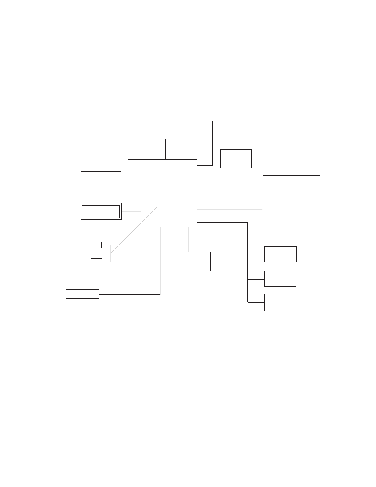
1. GENERAL
1-1. System chart
RAM610
4M bits
RAM530
1M bits
HHS-9
Scanner
QT-2046MC
MCR unit
MDL-8
Multi Drawer
2nd Display
QT-2000
Customer
Display
Pole
Cable SA-1062S
QT-2060D
Rear
Display
Clerk Key
CLK-K17 (6 clerk)
CLK-K18 (15 clerk)
QT-2063D
QT-2061S
KP-200 / KP-300
Kitchen Printer
SP-1200
Slip Printer
R/J Printer
TM-U950
TM-T85
TM-T88
SA-3015
TM-T85
UP-350
The QT-2000 has the following unique points:
(The system configuration is shown in the chart above.)
1. Separete R/J printer
2. Small foot-print and low-profile design
3. LCD display : Max. 2 LCD display
4. Flat keyboard menu holder : Max. 8 menu can be contorolled.
4 (direction) x 2 (holder)
5. Data backup function by EEPROM (Flash ROM)
6. Infrared communication interface
— 1 —
Page 4

1-2. Device list (Option)
No. Model Name Device Name Note
Sheet holder
1 SH-KIT1 Sheet holder kit 2 holders (1st - 4th, 5th - 8th)
Kitchen Printer
2 KP-200 Kitichen printer
3 KP-300 Kitchen printer with auto cutter
Slip printer
4 SP-1200 Slip printer
R/J printer
5 SA-3015 R/J and slip printer TM-U950 Paper size : 70mm
Dot matrix printer
6 TM-T85 Receipt printer TM-T85 Paper size : 80mm
Thermal printer
7 UP-350 Receipt printer TM-T88 Paper size : 80mm
Thermal printer
8 PS-150/PS-170 AC adaptor for TM-T85 / UP-350
9 SA-3087TM Printer cable for TM-T85 / UP-350
(Cable length : 3 m)
Display
10 QT-2062D Second LCD display
11 QT-2060D Rear display
12 QT-2063D Customer display
13 QT-2061S Pole for QT-2063D
14 SA-1062S Expantion cable for QT-2063D
(Cable length : 5 m)
Multi drawer
15 MDL-8 Multi drawer kit Additional 1 drawer
Memory
16 RAM-610-10LL RAM chip 4 M bits chip
17 RAM-530-10 RAM chip 1 M bits chip
MCR
18 QT-2046MC Magnetic card reader
Clerk key
19 CLK-K17 Clerk key kit for 6 clerk
20 CLK-K18 Clerk key kit for 15 clerk
Hand held scanner
21 HHS-9 scanner RS-232C
— 2 —
Page 5
2. SPECIFICATION
2-1. QT-2000
120V 230V
Power consumption In operation Max.: 0.7A 0.4A
Stand-by Max.: 0.4A 0.3A
Mode SW OFF Max.: 0.3A 0.2A
Memory Standard: 384 KB
Max: 1MB
Memory protection Back up battery Lithium-Banadium battery VL3032/S6A
Back up period 30 days ( 25°C )
Battery life Replace every 5 years
Charging time 48 hours for full charge
Clock and calender Accuracy within ±30 sec./month ( 25 °C )
Auto calender Effective 2099 A.D.
Environment Operating temperature 0°C ~ 40°C
Operating humidity 20% ~ 65%
Strorage temperature -20°C ~ 60°C
Storage humidity 10% ~ 80%
In the carton box : Storage temperature -20°C ~ 65°C
Storage humidity 10% ~ 80%
LCD display LCD life 15,000 hours
Back light Back light life 10,000 hours
Power prutection battery No function
CAUTION
Danger of explosion if battery is incorrectly replaced.
Replace only with the same or equivalent type
recommended by the manufacturer.
Dispose of used batteries according
to the manufacture’s instructions.
VORSICHT !
Explosionsgefahr bei unsachgemäßem Austausch der Batterie.
Ersatz nur durch denselben oder einen vom
Hersteller empfohlenen gleichwertigen Typ.
Entsorgung gebrauchter Batterien nach
Angaben des Herstellers.
ADVARSEL !
Lithiumbatteri - Eksplosionsfare ved fejlagtig hándtering.
Udskiftning má kun ske med batteri
af samme fabrikat og type.
Levér det brugte batteri tilbage til leverandØren.
— 3 —
Page 6

2-2. Printer
2-2-1. Model name : SA-3015
Item Description
Printer name TM-U950
Power source +24V DC ±10%
Current consumprion R/J Average : Approx. 1.8A Max : Approx. 8A
Print method Serial impact dot-matrix printer
MCBF 5,000,000 lines (auto-cutter and stamp once every 15 lines)
Print speed 233 CPS ( 9x9 dots : High speed )
Charactor per line R/J : 30 (9x9), 40 (7x9)
Stamp size 42 x 20 mm (Print area)
Roll paper Type : Fine quality paper ( Single layer only)
Slip paper Type : Plane paper, Carbon copy paper,
Ink ribbon Type : ERC-31
Interface Serial RS-232C interface
Slip Average : Approx. 2.3A
Standby : 0.3A
311 CPS ( 7x9 dots : Low speed )
Slip : 66 (9x9), 88 (7x9)
Width : 69.5 ±0.5 mm
Paper diameter : 83 mm or less
Paper thickeness : 0.06 to 0.09 mm
Pressure-sensitive paper
Number of paper : Original + 4 copies
Dimension : 70x70 to 210x297mm (WxH)
Thickness : 0.09 to 0.36mm
Ribbon life : 7,000,000 characters (18 dots per charactor)
2-2-2. Model name : TM-T85
Item Description
Printer name TM-T85
Power source +24V DC ±7%
Current consumprion Average : Approx. 1.3A Max : Approx. 6.0A
Standby : Approx. 0.1A
Print method Line thermal printing method
MCBF 3,500,000 lines (font A printing)
Print speed 12 lines/sec. (1/6 inch line feed)
13 lines/sec. (1/9 inch line feed)
Charactor per line 42 digits (12x24), 56 digits (9x7), 21 digits (24x24)
Print width 72mm
Roll paper Type : Prescribed thermal paper
Width : 80mm
Paper diameter : 83 mm or less
Paper thickeness : 65±5µ m
Interface Serial RS-232C interface
— 4 —
Page 7

2-2-3. Model name : UP-350 (TM-T88)
Item Description
Printer name TM-T88
Power source +24V DC ±7%
Current consumprion Average : Approx. 1.5A Max : Approx. 5.0A
Print method Line thermal printing method
MCBF 10,000,000 lines (font A printing)
Print speed High speed : 16.5 lines/sec. (1/6 inch line feed)
Charactor per line 42 digits (12x24), 56 digits (9x7)
Print width 72.2 ±0.2mm
Roll paper Type : Prescribed thermal paper
Interface Serial RS-232C interface
2-3. Slip printer
Model name : SP-1200
Standby : Approx. 0.2A
Low speed : 11.8 lines/sec. (1/6 inch line feed)
Width : 79.5±0.5mm
Paper diameter : 83 mm or less
Item Description
Printer name Model 290
Power source +24V DC ±10%
Print method Dot print ( with built-in shuttle head)
MCBF 1,500,000 lines
Print speed Approx. 2.3 to 1.9 lines/sec.
Charactor per line Max. : 35 digits (5x7)
Slip paper Type : Prescribed thermal paper
Carbon copy paper
Pressure-sensitive paper
Width : 80x80 to 182x257mm (WxL)
Number of paper : Max. : 3 sheets (Original + 2 copies)
Thickness : Total thickness : 0.35mm
Nomal paper : 0.09 to 0.25mm
Copy paper :Base sheet : 0.07 to 0.2mm
Duplicate : 0.04 to 0.07mm
Carbon paper : Approx 0.035mm
Ink ribbon Type : ERC-27
Ribbon life : 1,500,000 characters
Interface Serial interface
— 5 —
Page 8

2-4. Kitchen printer
Model name : KP-300
Item Description
Printer name DP-617
Power source AC115V / AC230V
Current consumprion 30w
Print method Serial impact printing method
MCBF Printer mechanism : 2,500,000 lines
Print speed 2.4 lines/sec.
Character per line 40 digits 400 dots/line
Roll paper Width : 76mm
Ink ribbon RE-1
Interface RS-422 interface
Model name : KP-200
Item Description
Printer name DP-575
Power source AC115V / AC230V
Current consumprion 25w
Print method Serial impact printing method
MCBF Printer mechanism : 1,500,000 lines
Print speed 1.2 lines/sec.
Character per line 40 digits
Roll paper Width : 69mm
Ink ribbon RB-2
Interface RS-422 interface
Both direction printing
Head : 50,000,000 character
Paper diameter : 80mm or less
1 direction printing ( L to R )
Head : 50,000,000 character
Paper diameter : 80mm or less
2-5. Hand scanner
Model name : HHS-9
Item Description
Power supply +5.0 V DC ± 5%
Power consumption Max. 0.4 W
Rush current Max. 1.5 A
Operating temperrature 0 to 40°C
Operating humidity 10 to 90% RH (not to condence dew)
Reading width 65 mm
Reading resolution less than 0.125 mm (NW-7,CODE39,ITF,STF)
PCS value 0.45 or more
less than 0.15 mm (CODE93,CODE128)
(wavelength 660 nm, white bar reflectivity ≥ 85%)
— 6 —
Page 9

2-6. MCR
Model name : QT-2046MC
Item Description
Model Name ZU-M1242S4
Card feed Manual operation
Data read direction One way (from right to left)
Read/Write Read only
Magnetic card ISO 7810 , ISO7811
Magnetic stripe encode Track 1: ISO1(IATA) Track 2 : ISO2(ABA)
Size 90 mm (L) x 25 mm (W) x 24 mm (H)
Weight About 28 g (Mechanisn only)
Power supply 5 V DC ± 10%, 6.0 mA (typ.) 9.0 mA (max.)
Feed speed 10 to 1500 mm/sec.
Life of magnetic head 300,000 pass (min.)
Life of electric circuit 50,000 hours
Error rate 1/1,000 (max.)
— 7 —
Page 10
3. QT-2000 CONNECTOR LOCATIONS
3-1. QT-2000 connector location
Power switch
RS-232C Com1
Slip printer port
RS-232C Com3
Bottom view
RS-232C Com2
In-lineKP In-line
Drawer cable
Infrared port
Com 1 : for hand held scanner HHS-9
Com 2 : for R/J printer (UP-350, SA-3015 and TM-T85)
Com 3 : for MODEM or PC
Power switch : for service maintenance
Make sure off this switch when open the machine.
Because, the power is applied even if the mode swith is off.
— 8 —
Page 11
3-2. Interface pin asignment
Com1: Hand held scanner HHS-9 (Location : CN2 on E580-CNB)
Pin No. Description
1 TXD1
2 RXD1
3 RTS1
4 CTS1
5 DSR1
6 DTR1
7 GND
8 NC
9 VCC
10 NC
11 GND
12 NC
13 NC
14 NC
15 GND
Com2 : R/J printer (Location : CN1 on E580-CNB)
Pin No. Description
1 NC
2 RXD2
3 TXD2
4 DTR2
5 GND
6 DSR2
7 RTS2
8 CTS2
9 NC
Com3 : Modem / PC (Location : CN4)
Pin No. Description
1 CD3
2 RXD3
3 TXD3
4 DTR3
5 GND
6 DSR3
7 RTS3
8 CTS3
9 CI3
— 9 —
Page 12
Slip printer : SP-1200 (Location : CN10)
Pin No. Description
1 VCC
2 VCC
3 Sensor signal
4 NC
5 VP
6 VP
7 VP
8 VP
9 Busy signal
10 NACK signal
11 GNDP
12 GNDP
13 Data signal
14 GNDP
15 NC
16 Clock signal
17 Clear signal
18 Reset signal
19 GNDP
20 GNDP
Kitchen printer : KP-200, KP-300 ( Location : CN2)
Pin No. Description
1 TXD (Red wire)
2 RXD (Black wire)
In-line I/F : C In-Line (ARCNET) (Location : CN2)
Pin No. Description
3 RXD (Black wire)
4 TXD (Red wire)
Drawer I/F (Location : DW1)
Pin No. Description
1 Drive signal (Red wire)
2 Power (Black wire)
3 Sensor siglal (Brown wire)
— 10 —
Page 13
4. INITIALIZE OPERATION
1
4-1.To initialize QT-2000 terminal
Preparation:
1. All peripheral devices and QT-2000 terminals of this cluster should be turned off.
2. Connect all of the peripheral devices (such as printer, display etc.) to QT-2000 terminal.
3. Connect all QT-2000 terminals by in-line.
Operation:
Date 00-00-00
Time 12:34 00
ID Character MC #01
Date 97-12-15
Check System Master
Time 12:34 00
KP System Master
R/J/Order Printer SA-3015
ID Character MC #01
Slip Printer SA-3015
Check System Master
Rear Display No
KP System Master
Remote Display No
R/J/Order Printer SA-3015
OK? Yes
Slip Printer SA-3015
Rear Display No
Remote Display No
OK? YES
4. Turn on all peripheral devices of a QT-2000 terminal.
5. Turn on this QT-2000 terminal with pressing the left-most
key of the top row and release the key after buzzer sounds.
6. After releasing the key, enter 10000 (for Eu/Di)/20000 (U.S.)
and press the right part of the <ST> key.
7. Enter the current date (YY/MM/DD order) and time and
press the <Yes> key.
Date 97-12-15
Time 12:34 00
ID Character MC #01
Check System Master
KP System Master
R/J/Order Printer SA-3015
Slip Printer SA-3015
Rear Display No
Remote Display No
OK? YES
Date 97-12-15
Time 12:34 00
ID Character MC #01
Check System Master
KP System Master
R/J/Order Printer SA-3015
Slip Printer SA-3015
Rear Display No
Remote Display No
OK? YES
Date 97-12-15
Time 12:34 00
ID Character MC #01
Check System Master
KP System Master
R/J/Order Printer SA-3015
Slip Printer SA-3015
Rear Display No
Remote Display No
OK? YES
8. In ID character field, the auto-defined ID No. is shown.
We recommend that you should not change the value.
9. In these fields, you can select
“1.Master/2.Backup Master/3.Satellite.”
Please select one of these options and press the <Yes> key.
10. In this field, you can select, “1.Non/2.UP-350/3.SA-3015”
for R/J/Order printer.
Please select one of these options and press the <Yes> key.
— 11 —
Page 14
Date 97-12-15
Time 12:34 00
ID Character MC #01
Check System Master
KP System Master
R/J/Order Printer SA-3015
Slip Printer SA-3015
Rear Display No
Remote Display No
OK? YES
11. In this field, you can select, “1.Non/2.SA-3015/3.SP-1200”
for slip printer.
Please select one of these options and press the <Yes> key.
Date 97-12-15
Time 12:34 00
ID Character MC #01
Check System Master
KP System Master
R/J/Order Printer SA-3015
Slip Printer SA-3015
Rear Display No
Remote Display No
OK? YES
Date 97-12-15
Time 12:34 00
ID Character MC #01
Check System Master
KP System Master
R/J/Order Printer SA-3015
Slip Printer SA-3015
Rear Display No
Remote Display No
OK? YES
Date 97-12-15
Time 12:34 00
ID Character MC #01
Check System Master
KP System Master
R/J/Order Printer SA-3015
Slip Printer SA-3015
Rear Display No
Remote Display No
OK? YES
12. In these fields, you can select, “1.Yes/2.No” for rear display
and remote display.
Please select one of these options and press the <Yes> key.
13. Please confirm all of the field and if they are all right, press
the <Yes> key to proceed the next step.
INIT 97-12-17 12:34 000000
AUTO PGM Start YES
14. If you want to download program data from other terminal,
press the <Yes> key and proceed the next step.
If you don't need to download any program data, just press the
<No> key (the initialization of this terminal is completed).
Return to step 4 to initialize other terminals.
— 12 —
Page 15
Program copy from other terminal.
gpy
INIT 97-12-15 12:34 000000
Received Data All PGM
PGM Receive from MC #05
OK? YES
INIT 97-12-15 12:34 000000
Received Data All PGM
PGM Receive from MC #05
OK? YES
15. In this field, you can select the receiving contents as
“1.All Data (including totalizer)/2.All PGM (program only).”
16. In this field, you should enter the source ID number of
the data and press the <Yes> key.
INIT 97-12-15 12:34 000000
Received Data All PGM
PGM Receive from MC #05
OK? YES
17. Please confirm all of the fields and if they are all right,
press the <Yes> key to proceed downloading.
After completion of downloading, return to step 4 to initialize
other terminals.
— 13 —
Page 16

4-2. To initialize QT-2000 terminal (add/replace one QT-2000)
Preparation:
1. All peripheral devices and QT-2000 terminals of this cluster should be turned off.
2. Connect all of the peripheral devices (such as printer, display etc.) to this QT-2000 terminal.
3. Connect this QT-2000 terminal to in-line.
Operation:
Date 00-00-00
Time 12:34 00
ID Character MC #01
Check System Master
Date 97-12-15
KP System Master
Time 12:34 00
R/J/Order Printer SA-3015
Slip Printer SA-3015
ID Character MC #01
Rear Display No
Check System Master
Remote Display No
KP System Master
OK? Yes
R/J/Order Printer SA-3015
Slip Printer SA-3015
Rear Display No
Remote Display No
OK? YES
4. Turn on all peripheral devices of this QT-2000 terminal.
And turn on all QT-2000 except this terminal of the cluster.
5. Turn on this QT-2000 terminal with pressing the left-most
key of the top row and release the key after buzzer sounds.
6. After releasing the key, enter 10000 (for Eu/Di)/20000 (U.S.)
and press the right part of the <ST> key.
7. Enter the current date (YY/MM/DD order) and time and
press the <Yes> key.
Date 97-12-15
Time 12:34 00
ID Character MC #01
Check System Master
KP System Master
R/J/Order Printer SA-3015
Slip Printer SA-3015
Rear Display No
Remote Display No
OK? YES
8. In ID character field, the auto-defined ID No. is shown.
Please check if the same value is set in this field.
We recommend that you should not change the value.
Date 97-12-15
Time 12:34 00
ID Character MC #01
Check System Master
KP System Master
R/J/Order Printer SA-3015
Slip Printer SA-3015
Rear Display No
Remote Display No
OK? YES
Date 97-12-15
Time 12:34 00
ID Character MC #01
Check System Master
KP System Master
R/J/Order Printer SA-3015
Slip Printer SA-3015
Rear Display No
Remote Display No
OK? YES
9. In these fields, you can select
“1.Master/2.Backup Master/3.Satellite.”
Please choose former options and press the <Yes> key.
10. In this field, you can select, “1.Non/2.UP-350/3.TM-U950”
for R/J/Order printer.
1
Please choose former option and press the <Yes> key.
— 14 —
Page 17
Date 97-12-15
Time 12:34 00
ID Character MC #01
Check System Master
KP System Master
R/J/Order Printer SA-3015
Slip Printer SA-3015
Rear Display No
Remote Display No
OK? YES
11. In this field, you can select, “1.Non/2.SA-3015/3.SP-1200”
for slip printer.
Please choose former options and press the <Yes> key.
Date 97-12-15
Time 12:34 00
ID Character MC #01
Check System Master
KP System Master
R/J/Order Printer SA-3015
Slip Printer SA-3015
Rear Display No
Remote Display No
OK? YES
Date 97-12-15
Time 12:34 00
ID Character MC #01
Check System Master
KP System Master
R/J/Order Printer SA-3015
Slip Printer SA-3015
Rear Display No
Remote Display No
OK? YES
Date 97-12-15
Time 12:34 00
ID Character MC #01
Check System Master
KP System Master
R/J/Order Printer SA-3015
Slip Printer SA-3015
Rear Display No
Remote Display No
OK? YES
12. In these fields, you can select, “1.Yes/2.No” for rear display
and remote display.
Please choose former options and press the <Yes> key.
13. Please confirm all of the field and if they are all right, press
the <Yes> key to proceed the next step.
INIT 97-12-17 12:34 000000
AUTO PGM Start YES
14.If you want to download program dasa from other terminal,
press the <Yes> key to proceed the next step.
If you don’t need to download any program data, just press the
<No> key (The initialization is completed).
— 15 —
Page 18
Program copy from other terminal.
INIT 97-12-15 12:34 000000
Received Data All PGM
PGM Receive from MC #05
OK? YES
INIT 97-12-15 12:34 000000
Received Data All PGM
PGM Receive from MC #05
OK? YES
15. In this field, you can select the receiving contents as
“1.AllData (including totalizer)/2.All PGM (program only).”
16. In this field, you should enter the source ID number of
the data and press the <Yes> key.
INIT 97-12-15 12:34 000000
Received Data All PGM
PGM Receive from MC #05
OK? YES
17. Please confirm all of the fields and if they are all right,
press the <Yes> key to proceed downloading.
After completion of downloading, the initialization opera-tion
is finished.
— 16 —
Page 19
4-3. To flag clear QT-2000 terminal (INIT2, Restore from flash)
Preparation:
1. All peripheral devices and this QT-2000 terminal should be turned off.
2. Check the connection of all peripheral devices (such as printer, display etc.) of this
QT-2000 terminal.
3. Check the connection of this QT-2000 terminal to in-line.
Operation:
15-12-97 12:34
INIT
1.Flag Clear
2.Init2
3.Restore
0.00
Note:
Performing “Init 2” requires password “8888888888” and
performing “Restore” requires password “0000000000.”
4. Turn on all peripheral devices of this QT-2000 terminal.
5. Turn on this QT-2000 terminal with pressing the right-most
key of the top row and release the key after buzzer sounds.
6. After releasing the key, press the right part of the <ST> key.
7. Select "1.Flag Clear" and press the <Yes> key.
The flag clear operation is finished.
— 17 —
Page 20
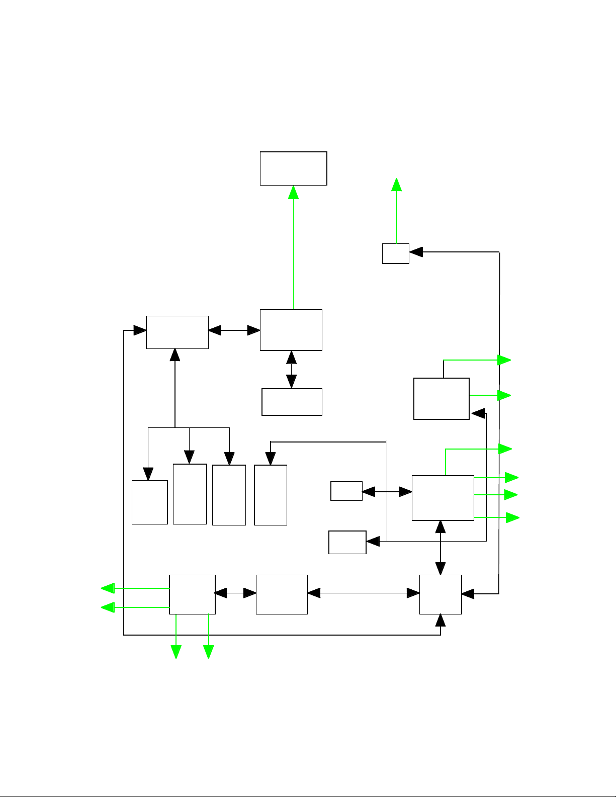
5. CIRCUIT EXPLANATION
y
y
y
5-1. Block diagram (MAIN PCB E580-1)
MASS memory
control
IC36
GA4
LCD displa
IC26
Display
controller
IC20
Video RAM
IN-LINE
ARCNET
IC10
ARCNET
Controller
IC11
GA2
Drawer
Keyboard
Kitchen
Printer
IR I/F
COM3
Modem
IC43
1M
SRAM
IC35 IC39 IC31
4M
SRAM
IC33
UART
COM2
Printer
1M
SRAM
COM1
Scanner
1M
EP ROM
IC32
GA3
IC22
16M F-ROM
IC23
2M SRAM
IC12
GA1
Slip
Printer
Back
Displa
Remort
Displa
IC6
CPU
— 18 —
Page 21
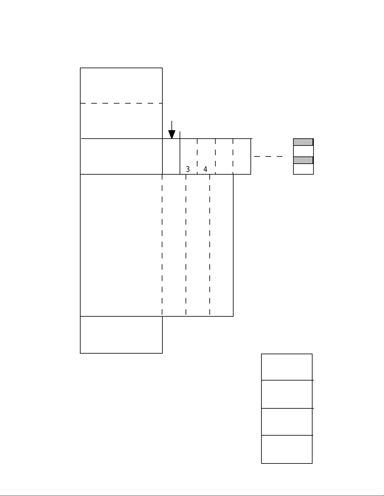
5-2. Memory map
00000h
20000h
40000h
60000h
80000h
SYSTEM RAM
2Mb x 1
RAM 1Mb x 1
16Mb FLASH ROM
Option RAM 1Mb
Option RAM 4Mb
2
1 3456
VRAM
256Kb x 2
Bank16
A0000h
C0000h
E0000h
FFFFFh
EP ROM
1Mb
Bank16 contents
40000h
VRAM
for LCD1
48000h
Control area
for LCD1
50000h
VRAM
for LCD2
— 19 —
Control area
for LCD2
58000h
Page 22
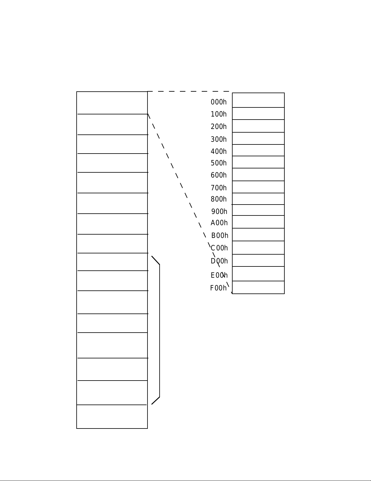
5-3. I/O Address map
W
W
Interrupt status port
There are 8 bits data for status per 1 port.
0000h
1000h
2000h
3000h
4000h
5000h
6000h
7000h
8000h
9000h
A000h
B000h
C000h
Rererved
(INT Status)
System
System
System
System
System
Reserved
Reserved
ARCNET R/
Back light control
for LCD1
Back light control
for LCD2
COM3 select
I/O port
000h
100h
200h
300h
400h
500h
600h
700h
800h
900h
A00h
B00h
C00h
D00h
E00h
F00h
System
Port #1
Port #2
Port #3
Port #4
Port #5
Port #6
Port #7
Port #8
Port #9
Port #10
Port #11
Port #12
Port #13
Port #14
Port #15
Users Area
( 15 ports )
D000h
E000h
F000h
FFFFh
Flash bank W
Future
Future
Reserved
— 20 —
Page 23
5-4. LSI pin description
1. CPU (uPD70108HGC-16-3B6)
Pin No. Name Description In/Out
1 A18/PS2 Address bus (A18) / Processor status Ou t
2 A17/PS1 Address bus (A17) / Processor status Ou t
3 A16/PS0 Address bus (A16) / Processor status Ou t
4 A1 5 Address bus (A15) Ou t
5 VDD Power source 6 VDD Power source 7 GND GND 8 GND GND -
9 IC Internaly connect (GND) 1 0 A1 4 Address bus (A14) Out
1 1 A1 3 Address bus (A13) Out
1 2 A1 2 Address bus (A12) Out
1 3 A1 1 Address bus (A11) Out
1 4 NC Not used 1 5 A1 0 Address bus (A10) Out
1 6 A9 Address bus (A9) Ou t
1 7 A8 Address bus (A8) Ou t
18 AD7 Address / Data bus (AD7) In/Out
19 AD6 Address / Data bus (AD6) In/Out
20 AD5 Address / Data bus (AD5) In/Out
21 AD4 Address / Data bus (AD4) In/Out
22 AD3 Address / Data bus (AD3) In/Out
23 AD2 Address / Data bus (AD2) In/Out
24 AD1 Address / Data bus (AD1) In/Out
25 AD0 Address / Data bus (AD0) In/Out
2 6 NC Not used 2 7 NC Not used 28 NMI Non-maskable interrupt (GND) 29 INT Maskable interrupt In
30 CLK System clock (16MHz) In
31 GND GND 3 2 NC Not used 33 GND GND 34 GND GND 35 RESET Reset In
36 READY Ready signal In
37 _POLL Polling signal In
3 8 _INTAK Interrupt acknowedge Out
39 ASTB Address strobe Ou t
4 0 NC Not used 4 1 _BUFEN Buffer enable Ou t
4 2 BUF_R/W Buffer read/write enable Out
43 IO/_M IO / memory select signal Out
44 _WR Write strobe Out
45 HLDAK Hold acknowlege Ou t
4 6 NC Not used 4 7 HLDRQ Hold request In
4 8 _RD Read strobe Ou t
4 9 S/_LG Small / Large select (5V) 50 LBS0 Not used 51 A19/PS3 Address bus (A19) / Processor status Ou t
5 2 NC Not used -
— 21 —
Page 24
(
)
2. GA1(MN53040KSF1)
Pin No. Name Description In/Out
1 E49MX2 Sub clock 4.92MHz Ou t
2 SVSS GND -
3 EADB0 Address bus (EADB0) Ou t
4 EADB1 Address bus (EADB1) Ou t
5 EADB2 Address bus (EADB2) Ou t
6 EADB3 Address bus (EADB3) Ou t
7 EADB4 Address bus (EADB4) Ou t
8 EADB5 Address bus (EADB5) Ou t
9 SVSS GND 10 EADB6 Address bus (EADB6) Ou t
11 EADB7 Address bus (EADB7) Ou t
12 EADB8 Address bus (EADB8) Ou t
13 EADB9 Address bus (EADB9) Ou t
14 EADB10 Address bus (EADB10) O u t
1 5 VDD VCC In
16 EADB11 Address bus (EADB11) O u t
17 VSS GND 18 EADB12 Address bus (EADB12) O u t
19 EADB13 Address bus (EADB13) O u t
20 EADB14 Address bus (EADB14) O u t
21 EADB15 Address bus (EADB15) O u t
22 EADB16 Address bus (EADB16) O u t
23 SVSS GND 24 EROMDC Direction select signal Out
25 _EMRD Output enable signal for system RAM Out
26 _EXINT Interruput signal from GA2,3,4 In
27 _EMWR Memory write signal Out
2 8 _ECGA2 Chip select signal for GA2 Out
29 _ERSET Reset signal In
30 _ECRA0 Bank select signal for RAM Out
31 _ECRA1 Bank select signal for RAM Out
32 _ECRA2 Bank select signal for RAM Out
33 _ECRA3 Bank select signal for RAM Out
34 EADB17 Address bus (EADB17) O u t
35 EADB18 Address bus (EADB18) O u t
36 EADB19 Not used 3 7 E1MN4M VCC In
38 _ECR04 Chip enable for ROM Out
39 _ECR03 Chip enable for FROM Out
40 _ECR02 Chip enable for FROM Out
41 _ECR01 Chip enable for FROM Out
42 _ECR00 Chip enable for FROM Out
43 _EIREQ VCC In
4 4 EIASTB GND In
45 EIHDAK GND In
46 VSS GND 4 7 _EIACK Not used O u t
4 8 VDD VCC In
4 9 EIHDRQ Not used Out
50 EAD0 Address / Data bus
AD0
In/Out
— 22 —
Page 25

Pin No. Name Description In/Out
y
51 EAD1 Address / Data bus (AD1) In/Out
52 EAD2 Address / Data bus (AD2) In/Out
53 EAD3 Address / Data bus (AD3) In/Out
54 EAD4 Address / Data bus (AD4) In/Out
55 EAD5 Address / Data bus (AD5) In/Out
56 SVSS GND 57 EAD6 Address / Data bus (AD6) In/Out
58 EAD7 Address / Data bus (AD7) In/Out
5 9 EA8 Address bus (A8) In
6 0 EA9 Address bus (A9) In
61 EA10 Address bus (A10) In
62 EA11 Address bus (A11) In
63 EA12 Address bus (A12) In
64 EA13 Address bus (A13) In
65 EA14 Address bus (A14) In
66 EA15 Address bus (A15) In
67 ECPURS Reset signal Out
68 EREADY Ready signal Out
69 EA16 Address bus (A16) In
70 EA17 Address bus (A17) In
71 EA18 Address bus (A18) In
72 EA19 Address bus (A19) In
73 _EINTA Interrupt acknowledge signal from CPU In
74 EASTB Address strobe signal In
75 EINT Interrupt signal to CPU Out
76 EINMCK IO / Memory select signal Out
77 VSS GND 7 8 _EINSD Not used Out
7 9 VDD VCC In
8 0 _EINRD VCC In
8 1 ESDEND Not used Out
82 _EKPSD Send data to kitchen printer Out
83 _EKPRD Receive data from kitchen printer In
84 EKPEND RTS signal for kitchen printer Out
85 ESD Send data for COM1 Out
86 ERD Receive data for COM1 In
87 _ECI VCC In
8 8 _EDR DSR signal for COM1 In
89 _EER DTR signal for COM1 Out
9 0 _ECD VCC In
91 _ECS CTS signal for COM1 In
92 _ERS RTS signal for COM1 Out
9 3 E16MX1 Main system clock 16MHz In
9 4 E16MX2 Main system clock 16MHz Out
95 SVSS GND 96 ECPURC CLock signal from CPU In
97 ECPUCK CLock signal from CPU Out
9 8 _FBFEN Buffer enable signal In
99 TEST2 GND In
100 EIONM IO / Memor
selection signal from CPU In
— 23 —
Page 26
Pin No. Name Description In/Out
y
y
)
101 EWR Write strobe signal from CPU I n
102 EHLADK Hold acknowledge signal from CPU In
103 EHLDRQ Hold request signal to CPU Out
104 _ERD Read signal In
105 _E1WT VCC In
106 _E2WT VCC In
107 _EDCR1 Data clear signal for back display Out
108 VDD VCC In
10 9 _EDNK1 Data NACK signal for back display In
110 VSS GND 111 EDDDAT Data signal for back display Out
112 EDDCLK Clock signal for back display Out
11 3 _EDNK2 Data NACK signal for remort display In
114 _EDCR2 Data clear signal for remort display Out
115 ESPBSY Busy signal for slip printer In
116 _ESPNK NACK signal for slip printer In
117 ESLPCR Data clear signal for slip printer Out
118 EPRDAT Data signal for slip printer Out
119 EPRCLK Clock signal for slip printer Out
120 ERJBSY GND In
121 _ERJNK Interrupt signal from ARCNET controller In
12 2 _ERJCR Not used O ut
12 3 TEST1 GND In
12 4 E49MX1 Sub s
stem clock 4.91MHz In
3. GA2 (MN53020KSK)
Pin No. Name Description In/Out
1 VSS GND -
2 XO Clock signal Out
3 _K13 Key input data signal (K13) In
4 _K12 Key input data signal (K12) In
5 _K11 Key input data signal (K11) In
6 _K10 Key input data signal (K10) In
7 _K9 Key input data signal (K9) In
8 _K8 Key input data signal (K8) In
9 _K7 Key input data signal (K7) In
10 _K6 Key input data signal (K6) In
11 _K5 Key input data signal (K5) In
12 _K4 Key input data signal (K4) In
13 _K3 Key input data signal (K3) In
14 _K2 Key input data signal (K2) In
15 _K1 Key input data signal (K1) In
16 _K0 Key input data signal (K0) In
17 _KO11 Key common signal (KO11) Out
18 _KO10 Key common signal (KO10) Out
19 _KO9 Key common signal (KO9) Out
20 _KO8 Ke
common signal (KO8
Out
— 24 —
Page 27

Pin No. Name Description In/Out
g
21 _KO7 Key common signal (KO7) Out
22 _KO6 Key common signal (KO6) Out
23 _KO5 Key common signal (KO5) Out
24 _KO4 Key common signal (KO4) Out
25 _KO3 Key common signal (KO3) Out
26 VSS GND 27 _KO2 Key common signal (KO2) Out
28 _KO1 Key common signal (KO1) Out
29 _KO0 Key common signal (KO0) Out
30 _INTPWD Power down signal In
31 AD7 Address / Data bus (AD7) In/Out
32 AD6 Address / Data bus (AD6) In/Out
33 AD5 Address / Data bus (AD5) In/Out
34 AD4 Address / Data bus (AD4) In/Out
35 AD3 Address / Data bus (AD3) In/Out
36 AD2 Address / Data bus (AD2) In/Out
37 VSS GND 38 AD1 Address / Data bus (AD1) In/Out
39 VDD VDD In
40 AD0 Address / Data bus (AD0) In/Out
4 1 _CRAM0 Chip select signal for system RAM Out
4 2 _CRAM1 Chip select signal for system RAM Out
4 3 _CRAM2 Nit used Ou t
4 4 CPUCLK Clock signal from CPU In
45 ASTB Address strobe signal from CPU In
46 _WR Write signal from CPU In
47 _RD Read signal from CPU In
48 ICEASTB GND In
49 _RAM3 Bank select signal In
5 0 NC Not used 51 VSS GND 5 2 _CRAM3 Not used O u t
53 _RAM2 Bank select signal for RAM In
54 _RAM1 Bank select signal for RAM In
55 _RAM0 Bank select signal for RAM In
56 _RESET Reset signal Out
5 7 _CSGA2 Chip select signal In
58 _MEMWR Memory write signal In
59 _INT Initilize signal Out
6 0 _REFRESH Not used O ut
6 1 _MEMWRT Not used Ou t
62 RFSEL VCC In
6 3 ITEST2 GND In
6 4 ITEST1 GND In
6 5 DIP8 Not used In
6 6 DIP7 Not used In
6 7 CASHSW6 Clerk switch signal I n
6 8 CASHSW5 Clerk switch signal In
6 9 CASHSW4 Clerk switch signal In
7 0 CASHSW3 Clerk switch si
nal In
— 25 —
Page 28

Pin No. Name Description In/Out
71 CASHSW2 Clerk switch signal In
7 2 CASHSW1 Clerk switch signal In
73 _SLIPSEN Sensor signal from slip printer In
74 OBRCLK Not used Out
7 5 OBRDATA VCC In
76 VSS GND 7 7 _DR4 Not used Ou t
7 8 _DR3 Not used Ou t
7 9 _DR2 Drawer open signal (DR2) Out
8 0 _DR1 Drawer open signal (DR1) Out
81 DRS Drawer sensor signal In
82 TAIWANJ GN D In
83 TAIWANR GND In
84 VLDSEN GND In
85 JPEND GND In
8 6 _PWON Not used Ou t
8 7 VDD VDD In
88 BUZER Buzzer signal Out
89 VSS GND 90 OFF GND In
91 PGM GND In
92 RF GND In
93 REG1 GND In
94 REG2 GND In
95 X Sheet select switch signal In
96 Z Sheet select switch signal In
97 XZ2 Sheet select switch signal In
98 _NACK Not used Ou t
99 XI Clock signal In
10 0 NC Not used -
— 26 —
Page 29
4. GA3 (MN53020KSG)
Pin No. Name Description In/Out
1 VSS GND -
2 XO Clock signal Out
3 SVDD VCC In
4 _CLOCK Not used Ou t
5 _ENABLE Not used Out
6 WMF1 GND In
7 WMF2 GND In
8 WMF3 GND In
9 WMF4 GND In
1 0 WMF5 GND In
1 1 WMF6 GND In
1 2 WMF7 GND In
1 3 WMF8 GND In
1 4 WMF9 GND In
15 _CLD2 Card loading signal In
16 _RCL2 Data sampling clock In
17 _RDT2 Data signal In
18 _CLD1 Card loading signal In
19 _RCL1 Data sampling clock In
20 _RDT1 Data signal In
21 _RESET Reset signal In
22 ASTB Address strobe signal In
2 3 _BUFEN Buffer enable signal In
24 BUFNRW Buffer read/write signal In
25 _WR Write signal In
26 VSS GND 27 INT Initilize signal Out
28 AD0 Address / Data bus (AD0) In/Out
29 AD1 Address / Data bus (AD1) In/Out
30 AD2 Address / Data bus (AD2) In/Out
31 AD3 Address / Data bus (AD3) In/Out
32 SVSS GND 33 AD4 Address / Data bus (AD4) In/Out
34 AD5 Address / Data bus (AD5) In/Out
35 AD6 Address / Data bus (AD6) In/Out
36 AD7 Address / Data bus (AD7) In/Out
37 VSS GND 38 AB8 Address signal (A8) In
39 VDD VCC In
40 AB9 Adress signal (A9) In
41 AB10 Adress signal (A10) In
42 AB11 Adress signal (A11) In
43 AB12 Adress signal (A12) In
44 AB13 Adress signal (A13) In
45 AB14 Adress signal (A14) In
46 AB15 Adress signal (A15) In
47 _RD Read signal In
48 ICEASTB GND In
49 IOM IO/Memory select signal In
5 0 NC Not used -
— 27 —
Page 30
Pin No. Name Description In/Out
51 VSS GND 52 USD0 Data bus for USART (USD0) In/Out
5 3 USD1 Data bus for USART (USD1) In/Out
5 4 USD2 Data bus for USART (USD2) In/Out
5 5 USD3 Data bus for USART (USD3) In/Out
5 6 USD4 Data bus for USART (USD4) In/Out
5 7 USD5 Data bus for USART (USD5) In/Out
58 SVSS GND 5 9 USD6 Data bus for USART (USD6) In/Out
6 0 USD7 Data bus for USART (USD7) In/Out
61 TOUT Not used Ou t
62 CLK Clock signal for USART Out
63 ADB0 Not used O ut
6 4 _RXC1 Not used Ou t
65 TXRDY1 Ready signal for IrDA or Com3 In
66 RXRDY1 GND In
67 _USART1 CH1 select signal for USART Out
68 _TXC1 Send clock signal for CH1 Out
69 _RXC2 Not used O ut
70 TXRDY2 Ready signal for Com2 In
71 RXRDY2 GND In
72 _USART2 CH2 select signal for USART Out
7 3 _TXC2 Not used Out
74 _ST2 VCC In
7 5 _RT VCC In
76 VSS GND 7 7 _CD VCC In
78 _CI VCC In
79 T3 GND In
80 SELECT GND In
8 1 PEND GND In
8 2 _FAULT VCC In
8 3 BUSY GND In
8 4 NACK VCC In
8 5 CENTD7 Not used O ut
8 6 CENTD8 Not used O ut
8 7 VDD VCC In
8 8 CENTD6 Not used O ut
89 VSS GND 9 0 CENTD4 Not used O ut
9 1 CENTD5 Not used O ut
9 2 CENTD3 Not used O ut
9 3 CENTD2 Not used O ut
9 4 CENTD1 Not used O ut
95 _STROBE Not used Ou t
96 _INT Not used Ou t
97 T2 GND In
98 T1 GND In
99 XIN Clock signal In
10 0 NC Not used -
— 28 —
Page 31

5. GA4 (MN56020KSJ)
Pin No. Name Description In/Out
1 VSS GND -
2 MD2 Data signal for MASS memory (MD2) In / Out
3 MD3 Data signal for MASS memory (MD3) In / Out
4 MD4 Data signal for MASS memory (MD4) In / Out
5 MD5 Data signal for MASS memory (MD5) In / Out
6 MD6 Data signal for MASS memory (MD6) In / Out
7 MD7 Data signal for MASS memory (MD7) In / Out
8 SVSS GND -
9 MA0 Address signal for MASS memory (MA0) Out
10 MA1 Address signal for MASS memory (MA1) Out
11 MA2 Address signal for MASS memory (MA2) Out
12 MA3 Address signal for MASS memory (MA3) Out
13 MA4 Address signal for MASS memory (MA4) Out
14 MA5 Address signal for MASS memory (MA5) Out
15 SVSS GND 16 MA6 Address signal for MASS memory (MA6) Out
17 MA7 Address signal for MASS memory (MA7) Out
18 MA8 Address signal for MASS memory (MA8) Out
19 MA9 Address signal for MASS memory (MA9) Out
20 SVSS GND 21 MA10 Address signal for MASS memory (MA10) Out
22 MA11 Address signal for MASS memory (MA11) Out
23 MA12 Address signal for MASS memory (MA12) Out
24 MA13 Address signal for MASS memory (MA13) Out
25 VSS GND 26 MA14 Address signal for MASS memory (MA14) Out
27 MA15 Address signal for MASS memory (MA15) Out
28 MA16 Address signal for MASS memory (MA16) Out
29 _INT Initilize signal Out
30 _RESET Reset signal In
31 AB19 Address bus (AB19) In
32 AB18 Address bus (AB18) In
33 AB17 Address bus (AB17) In
34 AB16 Address bus (AB16) In
35 AB15 Address bus (AB15) In
36 AB14 Address bus (AB14) In
3 7 VSSI GND 38 AB13 Address bus (AB13) In
39 AB12 Address bus (AB12) In
40 AB11 Address bus (AB11) In
41 AB10 Address bus (AB10) In
4 2 AB 9 Address bus (AB9) In
4 3 AB 8 Address bus (AB8) In
44 AD7 Address / Data bus (AD7) In / Out
45 AD6 Address / Data bus (AD6) In / Out
46 AD5 Address / Data bus (AD5) In / Out
47 AD4 Address / Data bus (AD4) In / Out
48 AD3 Address / Data bus (AD3) In / Out
49 AD2 Address / Data bus (AD2) In / Out
50 VDD VCC In
— 29 —
Page 32

Pin No. Name Description In/Out
51 VSS GND 52 AD1 Address / Data bus (AD1) In /Out
53 AD0 Address / Data bus (AD0) In / Out
5 4 _RFSHOT Not used Ou t
55 ASTB Address strobe signal In
56 IOXM IO / Memory select signal In
57 BUFXRW Buffer read/write signal In
5 8 CPUCLK Clock signal from CPU I n
5 9 _BUFEN Buffer enable signal In
60 _WR Write signal In
61 _RD Read signal In
62 _RFSH GND In
63 ICEAST GND In
6 4 TEST GND In
65 RW1 Memory write enable signal Out
6 6 RW2 Not used Ou t
67 _OE1 Memory output enable signal Out
68 _OE2 Not used Out
69 _CE0 Chip enable for MASS memory Out
70 _CE1 Chip enable for MASS memory Out
71 _CE2 Chip enable for MASS memory Out
72 _CE3 Chip enable for MASS memory Out
73 _CE4 Chip enable for MASS memory Out
74 _CE5 Chip enable for MASS memory Out
75 VSS GND 76 _CE6 Chip enable signal (Not used) 77 _CE7 Chip enable signal (Not used) 78 _CE8 Chip enable signal (Not used) 79 _CE9 Chip enable signal (Not used) 80 _CE10 Chip enable signal (Not used) 81 _CE11 Chip enable signal (Not used) 82 _CE12 Chip enable signal (Not used) 83 _CE13 Chip enable signal (Not used) 84 _CE14 Not used 85 _CE15 Chip select signal for LCD display Out
86 LS0 GND In
87 VDDI VCC In
88 LS1 VCC In
89 LS2 GND In
9 0 IOLS0 GND In
9 1 IOLS1 GND In
9 2 IOLS2 GND In
9 3 IOLS3 GND In
94 SELECT GND In
95 _INTIN VCC In
96 CEIN GND In
9 7 CEOT Not used Out
98 MD0 Data signal for MASS memory (MD0) In / Out
99 MD1 Data signal for MASS memory (MD1) In / Out
100 VDD VCC In
— 30 —
Page 33

6. NETWORK DRIVER (COM20020BILJP)
Pin No. Name In/Out Status Status Status Description
of OFF of ON of ON
No Token Token
1 A0/MUX In L L Pulse
2 A1 In L L L
3 A2/ALE In L L L
Input. On a non-multiplexed bus,
these signals are dirctly connectoed to
the low bits of the host address bus.
On a multiplexed address/data bus,
A0/MUX is tied low, A1 is left open,
and A2 is tied to the address latch
enable signal of the host. A1 is
connectoed to an internal pull-up
resistor.
4 AD0 In/Out L Pulse Pulse
5 AD1 In/Out L Pulse Pulse
6 AD2 In/Out L Pulse Pulse
8 D3 In/Out L Pulse Pulse
9 D4 In/Out L Pulse Pulse
10 D5 In/Out L Pulse Pulse
11 D6 In/Out L Pulse Pulse
12 D7 In/Out L Pulse Pulse
Input/Output. On a non-multiplexed
bus, these signals are used as the
data lines for the device. On a
multiplexed address/data bus,
AD0~AD2 act as the address lines
(latched by ALE) and as the low data
lines for the device. D3~D7 are
always used for data only. These
signals are connected to internal pull-
up resistors.
7,12,14 GND Power GND GND GND
16 XTAL1 In L Pulse Pulse
17 XTAL2 In L Pulse Pulse
Signal ground.
An external crystal shoul be connected
to these pins. If an external TTL clock
is used instead, it must be connected
to XTAL1 with a 390 ohms pull-up
resistor, and XTAL2 should be left
floating.
18 PULSE1 Out L H Pulse
19 PULSE2 Out L L L
Output. In normal mode, these active
low signals carry the transmit data
information, encoded in pulse format,
from the COM20020 to the media
driver circuitry. When the device is in
backplane mode, the PULSE1 signal
driver is programmable (push/pull or
open-drain), while the PULSE2 signal
provides a clock with frequency of
crystal/4. PULSE1 is connected to a
week internal pull-up resistor in
backplane mode.
20 RXIN In L H Pulse
Receive input. This signal carries the
receive data information from the line
receiver circuitry to the COM20020.
21 TXEN Out L L Pulse
Transmit Enable output. This signal
used in backplane mode to enable the
line drivers for transmission. The
polarity of the signal is programmable
by grounding the PULSE2 pin. This
option is valid only in backplane mode.
23 RESET IN In L H H
Input. This active low signal issued by
the microcontroller executes a hard-
ware reset. It is used to activate the
internal reset circuitry within the
COM20020.
— 31 —
Page 34

Pin No. Name In/Out Status Status Status Description
of OFF of ON of ON
No token Token
24 INTR Out L H Pulse
Interrupt output. This active low signal
is generated by the COM20020 when
an enabled interrupt condition occurs.
INTR returns to its inactive state when
the interrupt status condition or the
corresponding interrupt mask bit is
reset.
25 CS In L H Pulse
Chip select input. This active low
signal issued by the microcontroller
selects the COM20020 for an access.
26 WR/DIR In L Pulse Pulse
Input. On a 68XX-like bus, this signal
is issued by the microcontroller as the
Read/Write signal to determine the
direction of data transfer. In this case,
a logic "1" selects a read operation,
while a logic "0" selects a write operation. In this case, data is actually
strobed by the DS signal. On an
80XX-like bus, this active low signal is
isuued by the microcontroller to
indicate a write operation. in this
case, a logic "0" on this pin, when the
COM20020 is accessed, enables data
from the data bus to be written to the
device.
27 RD/DS In L L Pulse
Read/ Data strobe signal input. On a
68XX-like bus, this active low signal is
issued by the microcontroller as the
data strobe signal to strobe the data
onto the bus. On a 80XX-like bus, this
active low signal is issued by the
microcontroller to indicate a read
operation. In this case, a logic "0" on
this pin, when the COM20020 is
accessed, enables data from the
device to the data bus to be read by
the microcontroller.
15,18 VCC Power GND +5V +5V
Power supply +5V.
— 32 —
Page 35

5-5. Power down detection circuit
IC48 : Detection IC
The power is supplied at CN16 from switching power supply unit.
When the VP voltage become more than 22V, the voltage appears at pin No.2 of IC48 through
the zener diode ZD2.
The detection IC outputs "High" signal from pin No.6 and its signal going to IC45.
Then, the signal "INTPWD" becomes "High" and going to GA2.
The GA2 outputs "Reset" signal and reset the all GAs.
— 33 —
Page 36

5-6. Option RAM circuit
Standard memory capacity : 384 KB
To expand the memory capacity, put the option RAM chip on RAM1 or RAM2 position
Its convination is as follows;
Memory capacity Standard RAM1 RAM2
(Location : IC39) (Location : IC35)
384KB 384KB Nil Nil
512KB 384KB RAM530 Nil
1MB 384KB RAM530 RAM610
RAM530 : 1Mbits RAM (CXK581000P-10L)
RAM610 : 4Mbits RAM (CXK584000P-10LL)
— 34 —
Page 37

6. OPTION INSTALLATION
6-1. Clerk key unit (CLK-K17,CLK-K18)
1. Cut off the cable cover from the bottom case.
2. Release the screw which is fixing the keyboard and take tke keyboard out.
Cut the cable cover.
3. Insart the cable of clerk key unit and connect to CN5 of Main PCB.
CN5
Wire clamp
4. Tighten the screw to mount the clerk key unit.
Screw here.
Note :
Hold the cable using a wire
clamp to prevent the cut of wire.
— 35 —
Page 38
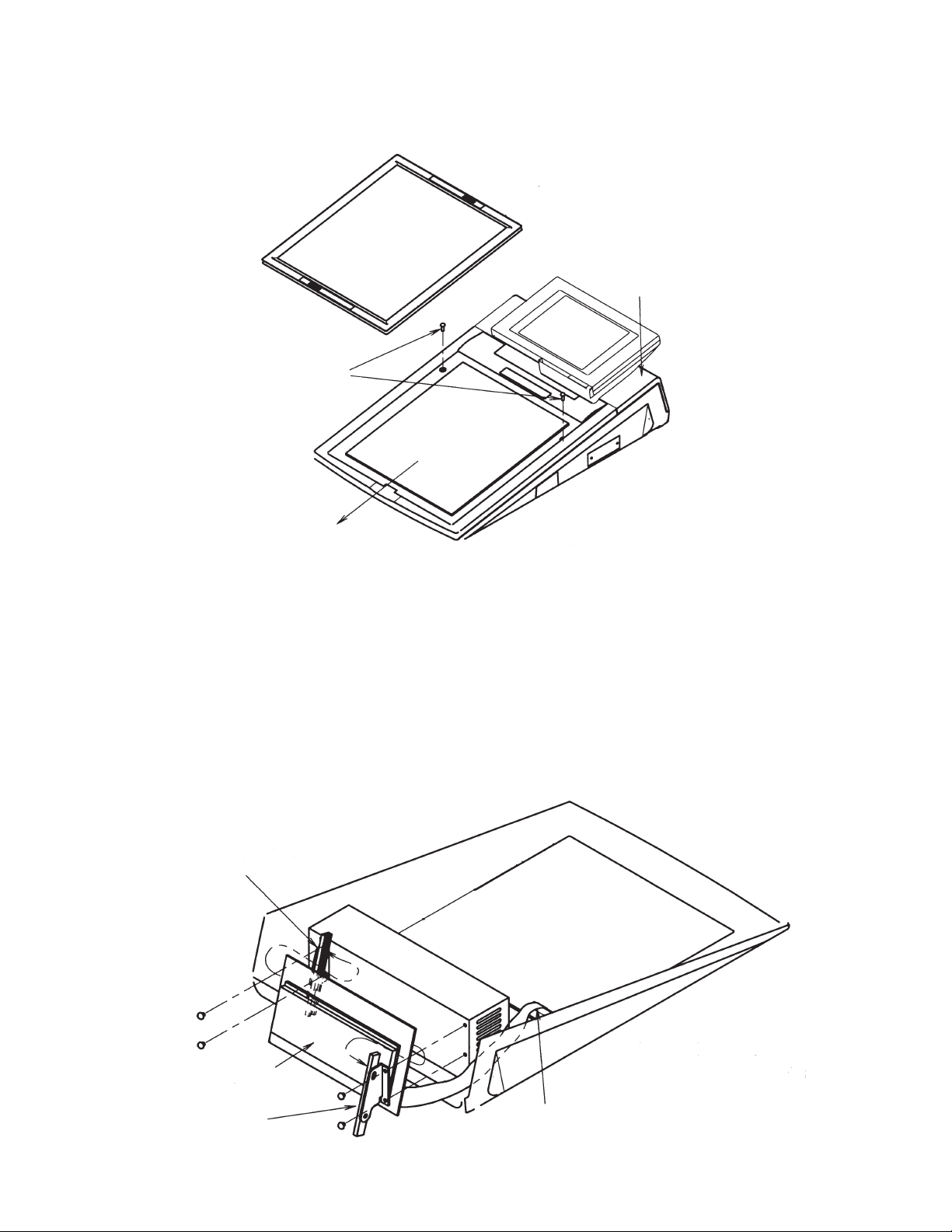
6-2. Rear Display (QT-2060D)
1. Release the screw which is fixing the keyboard and take tke keyboard out.
2. Remove the rear display window.
Rear display window
Release these screws
Slide the keyboard to the allow direction
3. Mount the display fixing plate (L).
4. Set the display PCB and display fixing plate (R), then tighten the screw.
5. Connect the display cable to CN15 of Main PCB.
Note :FG wire of the power code does not set behind displat PCB.
In case the FG wire is set behind the display PCB,the display might occurred flickering
problem.
Display fixing plate (L)
Display fixing plate (R)
CN15
— 36 —
Page 39

6-3. MCR Unit (QT-2046MC)
1. Release the screw which is fixing the keyboard and take tke keyboard out.
2. Remove the Main PCB and solder the connector which is in the QT-2046MC carton to the
location CN1 on Main PCB.
2. Mount the MCR unit on the lower case by screws and insart the cable to inside of the machine
from connector place.
4. Set the MAin PCB and connect the cable to CN1 on Main PCB.
Solder the connector here.
Cable for MCR is set
like this.
MCR mount stand
Screw here to mount
the MCR unit.
— 37 —
Page 40

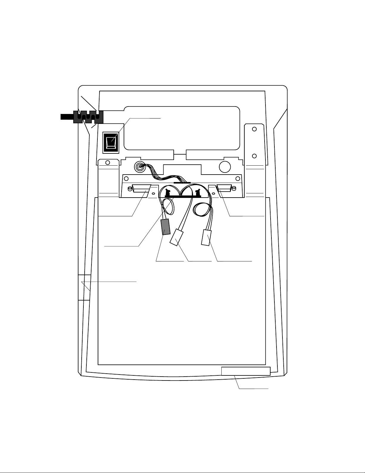
6-4. Multi drawer (MDL-8)
1. Release the screw which is fixing the keyboard and take tke keyboard out.
2. Round the cable of connector sub ass'y for drawer to ferrite core as following figure.
2. Remove the Main PCB and mount the following pars.
3. Connect the connector for FG to FG plate.
LocationCode No. Name Specification Q'ty
Q9 22304151 Transistor 2SD1853 1
D16 23010127 Diode 1SR35-100A 1
62195096 Connector sub ass'y for drawer E32564-2(#24-800) 1
62214686 connector for FG E31553-17(#20-800) 1
30304055 Ferrite core L5T18X6X10 1
Not used 26004918 Carbon film resistor R-25-1K-J 1
Not used 26007313 Carbon film resistor R-25-10K-J 1
51501640 Screw 3x10 ZMC-3 2
Location for mounting parts
Sloder the connector
ass'y for drawer here.
Round the cable of drawer connector.
Mount the transistor and diode here.
— 38 —
Page 41

7. IN / ON LINE
7-1. C-In line (ARCNET)
1) C-In line connection diagram
The maximum C-In line cable length and the maximum connection unit will be varied by the in-line
communication speed as shown below list.
[C-In line cable wiring]
Install the I/O-PB-12 in
the PC.
Note: When the cluster has more than 8 QT-2000 terminals,
all printer should be local printer.
When the cluster has less than or equal to 8 QT-2000
terminals, remote printer is allowable.
PC
In-line
Total Length : A
QT2000-1
R/J
R/JR/J
QT2000-32QT2000-4QT2000-3QT2000-2
R/JR/J
C-In line communication speed Maximum Maximum
(Baud rate) connection unit cable length A ( m )
1.25 M bps 8 86
625 K bps 12 200
312.5 K bps 20 430
156.25 K bps 32 890
Note : This C-In line system needs a I/O-PB-12 in the PC.
— 39 —
Page 42

2) C-In line cable, Connector, and Terminater
C-In line cable
Code No. Parts name Specification
1904 4023 In-line cable IPEV-SLA0.5x1P
C-In line connector(ECR side)
Code No. Parts name Specification
3500 5820 In-line connector kit XLP-KIT-1
C-In line connector (PC side)
Code No. Parts name Specification
1904 4069 Connector DE-9PF-N10
1904 4070 Junction shell DE-C8-J9-F1
Terminater
Code No. Parts name Specification
2600 2516 Carbon film resistor R-25-100-J
3) Termination point
ECRPC
ECR ECR
Terminater(100 ohms)
Terminater(100 ohms)
— 40 —
Page 43

4) Cable connection diagram (PC and MasterECR)
Signal Pin Signal Pin
SD 1 SD 1
RD 3 RD 2
FG FG plate FG Disconnect
(PC side) (ECR side)
Termination 'R in series are connected at pins
1 and 4 of two connectors at both the ends of
3
the in-line cable.
Fold the shield and fasten by
wrapping copper tape.
5)Cable connection diagram (Master ECR and Satellite ECR)
Red
Red
In-line cable
Wrap bent shield wire
with Copper tape
Shield wire
Black
Black
Terminator (100 ohms)
[Connection between PC and Master ECR]
Red
Red
In-line cable
Wrap bent shield wire
with Copper tape
Shield wire
Black
Black
In-line connector
In-line connector
— 41 —
Page 44
7-2. ON-line
Only the RS-232C Com3 port can be connected with a modem or perssonal computer.
1. Direct connection to PC
1-1. Connection layout
Up to 4 kitchen printers
KP KP KP
KP
PC
QT2000QT2000QT2000QT2000
KP/M CHK/BM CHK/M KP/BM
Slip SlipSlip
Using Com3 port
1-2. Cable wiring
QT-2000 (Com3) PC
Pin No. Signal name Pin No. Pin No. Signal name
3 SD / TXD 3 2 SD
2 RD / RXD 2 3 RD
7 RS / RTS 7 4 RS
8 CS / CTS 8 5 CS
1 CD / DCD 1 8 CD
4 ER / DTR 4 20 ER
6 DR / DSR 6 6 DR
9 CI / RI - 22 CI
5 GND 5 7 GND
R/J
(DSUB9) (DSUB25)
RS-232C
— 42 —
Page 45

2. MODEM system
nals
MAX : 15 m
Use Com2 or
Com3 port
2-1. Connection layout
.
Note: When the cluster has more than 8 QT-2000 terminals,
PC
on-line
2-2. Cable wiring
all printer should be local printer.
When the cluster has less than or equal to 8 QT-2000
terminals, remote printer is allowable.
R/JR/J
R/J
QT2000-32QT2000-3QT2000-2QT2000-1
R/J
QT-2000 (Com2) MODEM (DSUB25)
Pin No. Signal name Pin No. Signal name
3 SD/ TXD 2 SD
2 RD / RXD 3 RD
7 RS / RTS 4 RS
8 CS / CTS 5 CS
1 CD / DCD 8 CD
4 ER / DTR 20 ER
6 DR / DSR 6 DR
9 CI / RI 22 CI
5 GND 7 GND
QT-2000 (Com3) MODEM (DSUB25)
Pin No. Signal name Pin No. Signal name
3 SD/ TXD 2 SD
2 RD / RXD 3 RD
7 RS / RTS 4 RS
8 CS / CTS 5 CS
1 CD / DCD 8 CD
4 ER / DTR 20 ER
6 DR / DSR 6 DR
9 CI / RI 22 CI
5 GND 7 GND
— 43 —
Page 46

7-3. Kitchen printer connection
The kitchen printer control system requires a kitchen printer control master ( and back up master)
for kitchen printer control.
Maimum connection number : Max. 4 kitchen printer
Max. 4 terminals
1) Connection layout
Up to 4 kitchen printers
KP KP KP
KP/M CHK/BM CHK/M KP/BM
Slip SlipSlip
2) Connector and cable
Cable
Code No. Parts name Specification
1904 4023 In-line cable IPEV-SLA0.5x1P
KP
MAX : 1,000 m
R/J
Up to 4 QT-2000 terminals
PC
RS-232C
QT2000QT2000QT2000QT2000
Connector (ECR side)
Code No. Parts name Specification
3500 5820 In-line connector kit XLP-KIT-1
Connector (KP side)
Code No. Parts name Specification
1904 4069 Connector DE-9PF-N10
1904 4070 Junction shell DE-C8-J9-F1
— 44 —
— 44 —
Page 47

3) Cable connection diagram (ECR and Kitchen printer)
Signal Pin Signal Pin
SD 1 SD 1
RD 2 RD 3
FG FG plate FG Disconnect
(ECR side) (KP side)
[Connection for Kitchen printer side]
Termination 'R in series are connected at pins
Solder the cable as above wiring.
1 and 4 of two connectors at both the ends of
3
the in-line cable.
[Connection for ECR side]
In-line cable
Wrap bent shield wire
with Copper tape
Shield wire
Terminator (100 ohms)
Fold the shield and fasten by
wrapping copper tape.
Red
Red
Black
Black
In-line connector
— 45 —
Page 48

4) Kitchen printer controll setting
DIP switch setting for kitchen printer model KP-200 and KP-300 are as follows;
When the the DIP switch is changed, it is necessary to make initilize the kitchen printer.
Otherwise, DIp switch status can not read the CPU inside the controll board.
To make initilize, pressing "LF" button and power on the machine.
SW No.
1
2
3
4
5
6
KP-200 Bottom view
Machine number setting Baud rate setting
Kitchen printer
machine number
1
2
3
4
DIP SW No. DIP SW No.
1
2
3
4
OFF
OFF
OFF
OFF
ON
OFF
OFF
OFF
OFF
ON
OFF
OFF
ON
ON
OFF
OFF
7
8
Baud rate
600
1200
2400
4800
9600
Function
Machine number
Baud rate
5
OFF
ON
OFF
ON
OFF
6
OFF
OFF
ON
ON
OFF
Factory setting
OFF
OFF
OFF
OFF
ON
ON
OFF
OFF
7
8
OFF
OFF
OFF
OFF
OFF
OFF
OFF
OFF
ON
OFF
not used
}
KP-300 Bottom view
SW No.
1
2
Machine number
3
4
5
6
Baud rate
7
8
Machine number setting Baud rate setting
Kitchen printer
machine number
1
2
3
4
DIP SW No. DIP SW No.
1
2
3
4
OFF
OFF
OFF
OFF
ON
OFF
OFF
OFF
OFF
ON
OFF
OFF
ON
ON
OFF
OFF
— 46 —
Baud rate
600
1200
2400
4800
9600
Function
5
6
OFF
OFF
ON
OFF
OFF
ON
ON
ON
OFF
OFF
Factory setting
OFF
OFF
OFF
OFF
OFF
OFF
7
8
OFF
OFF
OFF
OFF
OFF
OFF
OFF
OFF
ON
OFF
ON
ON
not used
}
Page 49

8.DIAGNOSTIC PROGRAM
1. Starting the diagnostic program
(1)While holding down the button on the upper left corner (9 on the standard keyboard sheet), turn the power on.
(2)Release the button when the cash register beeps a buzzer sound.
(3)Using 10-key pad, input [9][9][9][9][9][0][0][0][0][0] then press [SUB TOTAL].
Note: While in the diagnostic mode, use the right half of the SUB TOTAL button for [SUB TOTAL] operations.
2. List of the diagnoses
Command
code
1 Rear display n01
2 Remote display n02
3 RJ printer n03 RS-232C COM2 test
4 Slip printer n04
5 Keyboard n05 buttons 1 to 168 check
6 OBR n06 RS-232C COM1 test.
7 MCR n07 Use checker magnetic card.
9 Drawer n09
10 Buzzer n10
11 Switches 11
12 Clock n12
Device to be checked Operation Note
Use checker bar code.
13 ROM n13 EPROM (128kB) x 1
14 RAM n14 Read/Write check
15 RAM n15 Read check
16 MRAM n16 Read/write check
17 MRAM n17 Read check
20 Low-Inline nm20 Transmit check
21 Low-inline nm21 Receive check
25 Async online m25 Loop back test
30 Infrared port 30 Infrared port receive test
31 Infrared port n31 Infrared port transmit test
— 47 —
Page 50

Command
code
32 Standard LCD n32
33 Optional LCD n33
34 Flash memory 34 Read/Write/Clear test
38 ARCNET n38 ARCNET ID set
39 ARCNET n39 ARCNET baud rate, token
40 ARCNET 40 ARCNET token stop
41 ARCNET nm41 ARCNET data transmit
42 ARCNET nm42 ARCNET data receive
3. Diagnoses
(1) Dot/7-segment display test
Operation: [n][0][1][SUB TOTAL] (for the rear display)
Device to be checked Operation Note
[n][0][2][SUB TOTAL] (for the remote display)
n = Number of execution and should be within the range of 0 to 9.
If no number or “0” is input, the test continues endlessly.
To stop the test, press [ESC].
Display: <LCD> <Dot/7-segment>
ABCDEFGHIJKLMNOP
0,12,34,56,78,90,
abcdefghijkolmnop
12,34,56,78,90,1
Prints “END *01” when the test is finished.
RJ Print:
SUB DISP
Displays “END *01” when the test is finished.
SUB DISP *01
* Displays or prints 02 while testing a remote display.
*
01
Displays alternately
— 48 —
Page 51

(2) R/J Printer test (RS-232C COM2)
Prints B’s on RS-232C printer for specified times.
Operation: [n][0][3][SUB TOTAL]
n = Number of execution and should be within the range of 0 to 9.
If no number or “0” is input, the test continues endlessly.
To stop the test, press [ESC].
Display: <LCD> <Dot/7-segment>
R/J 03
R/J 03
R/J 03
R/J 03
END 03
R/J print:
R/J 03
BBBBBBBBBBBBBBBBBBBBBBBBBBBBBBBBBBBBBBBB
BBBBBBBBBBBBBBBBBBBBBBBBBBBBBBBBBBBBBBBB
BBBBBBBBBBBBBBBBBBBBBBBBBBBBBBBBBBBBBBBB
BBBBBBBBBBBBBBBBBBBBBBBBBBBBBBBBBBBBBBBB
BBBBBBBBBBBBBBBBBBBBBBBBBBBBBBBBBBBBBBBB
BBBBBBBBBBBBBBBBBBBBBBBBBBBBBBBBBBBBBBBB
BBBBBBBBBBBBBBBBBBBBBBBBBBBBBBBBBBBBBBBB
BBBBBBBBBBBBBBBBBBBBBBBBBBBBBBBBBBBBBBBB
(3) Slip Printer test
Prints a test pattern on the slip printer for specified times and releases the slip.
Number of
execution
0
Dot/7-segment display indicates 0 only when
the test is continued from the “Dot/7-segment
display test.” When the test is performed
indipendently, the dot/7-segment display indicates nothing.
R/J Printer; TM-950 (2-sheet dot printer)
Partial cut (TM-950 printer prints “B” on the most significant digit)
Feed
Full cut (TM-950 printer prints “A” on the most significant digit)
0
TM-T85 (1-sheet thermal printer)
Operation: [n][0][4][SUB TOTAL]
n = Number of execution and should be within the range of 0 to 9.
If no number or “0” is input, the test continues endlessly.
To stop the test, press [ESC].
Display: <LCD> <Dot/7-segment>
slip 04
END 04
0
Slip print:
SLIP TEST PRINT
BBBBBBBBBBBBBBBBBBBBBBBB 8888888888
— 49 —
Dot/7-segment display indicates 0 only when
the test is continued from the “Dot/7-segment
display test.” When the test is performed
indipendently, the dot/7-segment display indicates nothing.
Release
0
Page 52

(4) Keyboard test
The display shows pressed button number when the key switch functions correctly.
Operation: [0][5][SUB TOTAL]
Press buttons and make sure that the pressed button number is displayed on the LCD.
Note:As [ESC] (button number159) button exits the diagnosis program, press [ESC] at the end.
Display: <LCD> <Dot/7-segment>
R/J Print:
KEY 05
KEY –– 26
KEY –– 27
KEY –– 28
KEY –– 29
KEY –––30
KEY 05
END 05
<Button numbers>
0
Dot/7-segment display indicates 0 only when
the test is continued from the “Dot/7-segment
display test.” When the test is performed
indipendently, the dot/7-segment display indicates nothing.
“END 05” will be displayed and
printed when [ESC] (button number
159) is pressed.
— 50 —
Press this button at the
end.
Page 53

(5) OBR test
Use only the checker bar code in which data 49401387 is written.
The program checks if the read data is 49401387.
Operation: [n][0][6][SUB TOT AL]
n = Number of execution and should be within the range of 0 to 9.
If no number or “0” is input, the test continues endlessly.
To stop the test, press [ESC].
Display: <LCD> <Dot/7-segment>
R/J Print:
OBR 06
OBR OK
OBR NG
FF4902580300562
END 06
OBR 06
OBR OK
OBR NG
When the read data is correct.
When the read data is incorrect.
Read data
0
When the read data is correct.
When the read data is incorrect.
0
Dot/7-segment display indicates 0 only
when the test is continued from the “Dot/
7-segment display test.” When the test
is performed indipendently, the dot/7segment display indicates nothing.
— 51 —
Page 54

(6) MCR test
Use only the checker magnet card.
Operation: [n][0][7][SUB TOTAL]
n = Number of execution and should be within the range of 0 to 9.
If no number or “0” is input, the test continues endlessly.
To stop the test, press [ESC].
Display: <LCD> <Dot/7-segment>
MCR 07
#1:OK #2:OK
#1:NG #2:NG
MCR#1
MCR#2
END 07
When the read data is incorrect, display indicates NG
and shows read data.
0
R/J Print:
MCR 07
#1:OK #2:OK
END 07
(7) Drawer test
Opens two drawers (multi drawer is optional) and shows open sensor status on the LCD.
Operation: [n][0][9][SUB TOTAL]
n = Number of execution and should be within the range of 0 to 9.
If no number or “0” is input, the test continues endlessly.
To stop the test, press [ESC].
“NG” when incorrect
Dot/7-segment display indicates 0 only when
the test is continued from the “Dot/7-segment
display test.” When the test is performed
indipendently, the dot/7-segment display indicates nothing.
Note: When MCR read error occurs, the display indicates “MCR READ ERR.”
0
Display: <LCD> <Dot/7-segment>
DRAWER 09
DRAWER: OPEN
END 09
R/J Print:
DRAWER 09
END 09
“NOT OPEN” when drawer does
not open
0
— 52 —
Dot/7-segment display indicates 0 only when
the test is continued from the “Dot/7-segment
display test.” When the test is performed
indipendently, the dot/7-segment display indicates nothing.
0
Page 55

(8) Buzzer test
Beep every 100 milliseconds. In one test, 2 buzzer sound.
Operation: [n][1][0][SUB TOT AL]
n = Number of execution and should be within the range of 0 to 9.
If no number or “0” is input, the test continues endlessly.
To stop the test, press [ESC].
Display: <LCD> <Dot/7-segment>
BUZZ 10
END 10
0
R/J Print:
BUZZ 10
END 10
(9) Switch test
Displays statuses of the switches and sensors of the connected devices.
Operation: [1][1][SUB TOTAL]
To stop the test, press [ESC].
Display: <LCD> <Dot/7-segment>
Keyboard Sheet 1 - 8
Not used
Not used
Slip paper sensor (0: slip inserted, 1: no slip inserted)
Drawer open sensor (0: close, 1: open)
Clerk key (00: not used, 01 - 15: clerk key no.)
No used
Dot/7-segment display indicates 0 only when
the test is continued from the “Dot/7-segment
display test.” When the test is performed
indipendently, the dot/7-segment display indicates nothing.
0
R/J Print:
STSW
0 0 0 0 0 0 1 00
END
STSW 11
END 11
11
11
0
Dot/7-segment display indicates 0 only when
the test is continued from the “Dot/7-segment
display test.” When the test is performed
indipendently, the dot/7-segment display indicates nothing.
— 53 —
Page 56

(10) Clock test
Operation: (1)Press [0][1][2][SUB TOTAL]
Display indicates date 99 12 31 MON, time 23 59 55.
If [1] is input instead of the first [0], the display shows the present time.
<LCD> <Dot/7-segment>
R/J Print:
CLOCK 12
99 12 31 MON
23 59 55
(2)Turn the power off.
(3)After for a while, turn the power on and
make sure that the time has been counted
while the register is off.
CLOCK 12
00 01 01 TUE
00 01 21
(4)Press [ESC] to exit from the program.
CLOCK 12
END 12
Counts up
Counts up
0
Dot/7-segment display indicates 0 only when
the test is continued from the “Dot/7-segment
display test.” When the test is performed
indipendently, the dot/7-segment display indicates nothing.
— 54 —
Page 57

(11) ROM test
Performs check sum test of the EPROM. Checks all the files written in the ROM and when an error occurs, the LCD
indicates the faulty file name and starting address of the file.
Operation: [n][1][3][SUB TOT AL]
n = Number of execution and should be within the range of 0 to 9.
If no number or “0” is input, the test continues endlessly.
To stop the test, press [ESC].
<LCD> <Dot/7-segment>
0
R/J Print:
ROM 13
config
cpyright
cmndrv.exe
ker.exe
tbox.exe
File names
Hndl580.exe
After the test, display indicates the result.
<LCD>
tbox.exe
hndl580.exe
diag580.exe
$tp.exe
config.env
ini.exe
ROM SUM CHECK OK
CREATE 97-04-17 11:53
Copywright (C) 1997
CASIO COMPUTER CO., LTD
All rights reserved.
ROM VER. AAFAB3075
END 13
Indicates “ESC” when the test is finished forcibly by [ESC].
0
ROM 13
config
cpyright
cmndrv.exe
fsys.exe
ker.exe
tbox.exe
hndl580.exe
diag580.exe
$tp.exe
config.env
ini.exe
ROM SUM CHECK OK
CREATE 97-04-17 11:53
Copyright (C) 1997
CASIO COMPUTER CO.,LTD
All rights reserved.
ROM VER. AAFAB 3075
END 13
Dot/7-segment display indicates 0 only when
the test is continued from the “Dot/7-segment
display test.” When the test is performed
indipendently, the dot/7-segment display indicates nothing.
— 55 —
Page 58
(12) RAM Read/Write test
Performs read after write test on RAM addresses 20000H to 3FFFF.
Operation: [n][1][4][SUB TOTAL]
n = Number of execution and should be within the range of 0 to 9.
If no number or “0” is input, the test continues endlessly.
To stop the test, press [ESC].
Display: <LCD> <Dot/7-segment>
R/J print:
RAM 14
RAM#2 OK
RAM#2 OK
RAM#2 OK
END 14
Number of execution.
Indicates “NG” when the
RAM is faulty.
0
Dot/7-segment display indicates 0 only when
the test is continued from the “Dot/7-segment
display test.” When the test is performed
indipendently, the dot/7-segment display indicates nothing.
0
RAM 14
RAM#2 OK
RAM#2 OK
“NG” when the RAM is
faulty
RAM#2 OK
END 14
(13) RAM Read test (memory backup test)
The program checks if RAM contents stored at the “RAM read/write test” are backed up after turning the power off.
Operation: (1)After the above “RAM Read/Write test”, turn the power off.
(2)After for a while, turn the power on then press [n][1][5][SUB TOTAL].
n = Number of execution and should be within the range of 0 to 9.
If no number or “0” is input, the test continues endlessly.
To stop the test, press [ESC].
Display: <LCD> <Dot/7-segment>
RAM 15
R/J print:
RAM#2 OK
RAM#2 OK
RAM#2 OK
END 15
Number of execution.
Indicates “NG” when the
RAM is faulty.
0
Dot/7-segment display indicates 0 only when
the test is continued from the “Dot/7-segment
display test.” When the test is performed
indipendently, the dot/7-segment display indicates nothing.
RAM 15
RAM#2 OK
RAM#2 OK
“NG” when the RAM is
faulty
RAM#2 OK
END 15
— 56 —
0
Page 59

(14) Mass RAM Read/Write test
Using the gate array and the CPU in QT-2000 circuit, the program performs RAM’s mass data (in 128k byte unit)
read after write test. The program does not diagnose VRAMs.
Operation: [n][1][6][SUB TOTAL].
n = Number of execution and should be within the range of 0 to 9.
If no number or “0” is input, the test continues endlessly.
To stop the test, press [ESC].
Display: <LCD> <Dot/7-segment>
RAM 16
MASS RAM CHIPS : m
m= bank number
0
MASS#m
Dot/7-segment display indicates 0 only when
the test is continued from the “Dot/7-segment
display test.” When the test is performed
indipendently, the dot/7-segment display indi-
R/J print:
MASS#m OK
END 16
or “NG”
Indicates “ESC” when
the test is finished
forcibly by [ESC].
0
cates nothing.
MASS 16
m= bank number
MASS RAM CHIPS : m
MASS#m OK
END 16
or “NG”
prints “ESC” when the
test is finished forcibly
by [ESC] button.
(15) Mass RAM backup test
The program checks if the memory contents stored in “Mass RAM read/write test” are backed up after power is
turned off then on again.
Operation: (1)After the above “RAM Read/Write test”, turn the power off.
(2)After for a while, turn the power on then press [n][1][7][SUB TOTAL].
n = Number of execution and should be within the range of 0 to 9.
If no number or “0” is input, the test continues endlessly.
To stop the test, press [ESC].
Display: <LCD> <Dot/7-segment>
MASS 17
MAS#m
MAS”m OK
END 17
R/J print:
m= bank number
or “NG”
Indicates “ESC” when
the test is finished
forcibly by [ESC].
0
Dot/7-segment display indicates 0 only when
the test is continued from the “Dot/7-segment
display test.” When the test is performed
indipendently, the dot/7-segment display indicates nothing.
MASS 17
MASS#m OK
END 17
m= bank number
or “NG”
prints “ESC” when the
test is finished forcibly
by [ESC] button.
— 57 —
0
Page 60

(16) Low inline data transmission test
Connect two QT-2000s with a standard inline cable (RS-485).
Inline cable: RS-485
C
7
8
9
4
5
6
1
2
3
0
00
•
C
7
8
9
4
5
6
1
2
3
0
00
•
Sender
Command code: 20
Perform the reception unit operation first then the transmission unit.
Operation: [n][m][2][0][SUB TOTAL]
n = Number of execution and should be within the range of 0 to 9.
If no number or “0” is input, the test continues endlessly.
m = baud rate (m > n) ; 0 : 1200 bps, 1: 2400 bps, 2: 4800 bps, 4: 9600 bps, 5: 19200 bps
To stop the test, press [ESC].
Reciever
Command code: 21
Display: <LCD> <Dot/7-segment>
L INLINE TX 20
OK: XX NG: XX
END 20
count up
Indicates “ESC” when
the test is finished
forcibly by [ESC].
0
Dot/7-segment display indicates 0 only when
the test is continued from the “Dot/7-segment
display test.” When the test is performed
indipendently, the dot/7-segment display indi-
R/J print:
cates nothing.
L INLINE TX 20
END 20
prints “ESC” when the
test is finished forcibly
by [ESC] button.
0
— 58 —
Page 61

(17) Low inline data reception test
Connect two QT-2000s with a standard inline cable (RS-485).
Perform the reception unit operation first then the transmission unit.
Operation: [n][m][2][1][SUB TOTAL]
n = Number of execution and should be within the range of 0 to 9.
If no number or “0” is input, the test continues endlessly.
m = baud rate (m > n) ; 0 : 1200 bps, 1: 2400 bps, 2: 4800 bps, 4: 9600 bps, 5: 19200 bps
To stop the test, press [ESC].
Display: <LCD> <Dot/7-segment>
L INLINE RX 21
OK: XX NG: XX
END 21
count up
Indicates “ESC” when
the test is finished
forcibly by [ESC].
R/J print:
L INLINE TX 21
END 21
prints “ESC” when the
test is finished forcibly
by [ESC] button.
(18) Asynchronous online test (loop back test)
Prepare the loop back connector.
Loop back connector wiring.
Pin No. 2: RD
3: SD
7: RTS
8: CTS
0
0
Dot/7-segment display indicates 0 only when
the test is continued from the “Dot/7-segment
display test.” When the test is performed
indipendently, the dot/7-segment display indicates nothing.
1: CD
4: DTR
6: DSR
9: CI
— 59 —
Page 62

Connect a loop back connector on COM3 port and perform the loop back test.
Operation: [m][2][5][SUB TOTAL]
m = baud rate ; 0: 1200 bps, 1: 2400 bps, 2: 4800 bps, 4: 9600 bps, 5: 19200 bps, 6:38400 bps
To stop the test, press [ESC].
Display: <LCD> <Dot/7-segment>
ASYNC ONLINE 25
OK: XX NG: XX
count up
0
ESC 21
0
Dot/7-segment display indicates 0 only when
the test is continued from the “Dot/7-segment
display test.” When the test is performed
indipendently, the dot/7-segment display indi-
R/J print:
cates nothing.
ASYNC ONLINE 25
ESC 25
(19) Infrared
Prepare two units of QT-2000 and set both units on the diagnostic mode. Face both units so that they can communicate by the infrared ports.
Prepare 2 machine and touch each IR I/F.
IR I/F
Sender
Command code: 30
Reciever
Command code: 31
C
7
8
9
4
5
6
1
2
3
0
00
•
— 60 —
Page 63

Operation: (1)On the receiving unit, press [3][0][SUB TOTAL].
The LCD on the receiving unit indicates;
ASYNC RX 30
✼
ESC 30
0
(2)On the transmission unit, press [n][3][1][SUB TOTAL].
n= Number of execution and should be within the range of 0 to 9.
If no number or “0” is input, the test continues endlessly.
To stop the test, press [ESC].
Display <LCD> <Dot/7-segment>
ASYNC TX/RX 31
OK: XX NG: XX
END 31
ASYNC TX/RX 31
OK: XX NG: XX
END 31
count up
Indicates “ESC” when
the test is finished
forcibly by [ESC].
Prints “ESC” when the
test is finish forcibly by
[ESC] button.
0
0
Dot/7-segment display indicates 0 only when
the test is continued from the “Dot/7-segment
display test.” When the test is performed
indipendently, the dot/7-segment display indicates nothing.
— 61 —
Page 64

(20) LCD test
Operation: [n][3][2][SUB TOTAL] (for standard LCD)
[n][3][3][SUB TOTAL] (for optional LCD)
n = Number of execution and should be within the range of 0 to 9.
If no number or “0” is input, the test continues endlessly.
To stop the test, press [ESC].
Display: <LCD>
R/J print
Repeats “n” times
LCD 32
END 32
— 62 —
Page 65

(21) Flash memory read/write/clear test
Performs read after write check on each bank of the flash memory. At the end of the test, all the data in the flash
memory are cleared.
The following table illustrates the relation between the address and the bank of the flash memory.
60000h
80000h
A0000h
C0000h
E0000h
Operation: [3][4][SUB TOTAL]
To stop the test, press [ESC].
Display: <LCD> <Dot/7-segment>
Flash 34
BANK#1 OK
BANK#2 OK
BANK#3 OK
BANK#4 OK
BANK#5 OK
or “NG”
...........
BANK#32 OK
END 34
Bank 1 Bank 9 Bank 17 Bank 25
Bank 2 Bank 10 Bank 18 Bank 26
Bank 3 Bank 11 Bank 19 Bank 27
Bank 4 Bank 12 Bank 20 Bank 28
Bank 5 Bank 13 Bank 21 Bank 29
Bank 6 Bank 14 Bank 22 Bank 30
Bank 7 Bank 15 Bank 23 Bank 31
Bank 8 Bank 16 Bank 24 Bank 32
Dot/7-segment display indicates 0 only when
the test is continued from the “Dot/7-segment
display test.” When the test is performed
indipendently, the dot/7-segment display indicates nothing.
0
0
R/J print:
FLASH 34
BANK#1 OK
BANK#2 OK
BANK#3 OK
or “NG”
...................
BANK#32 OK
END 34
— 63 —
Page 66

(22) ARCNET test-1 (ID number setting)
Sets ID number of ARCNET. Be sure to perform this program before doing the following ARCNET tests.
Operation: [m][m][m][3][8][SUB TOTAL]
mmm = ID number (001 to 253)
Display: <LCD> <Dot/7-segment>
ARC - ID 38
ARCNET MY - ID: xxx
END 38
R/J print:
ARC-ID 38
END 38
(23) ARCNET test-2 (baud rate setting, ARCNET communication)
After setting the baud rate, QT-2000s in the ARCNET start communications.
Operation: [n][3][9][SUB TOTAL]
n = baud rate; 0: 156.25kbps, 1: 312.5kbps, 2: 625kbps, 3: 1.25Mbps
Display: <LCD> <Dot/7-segment>
ARC–BPS 39
OK
END 39
R/J print:
ARC–BPS 39
END 39
ID No. ; 1 to 253
Indicates “INVALID ID XXX”
when invalid number is input.
or “NG”
0
0
Dot/7-segment display indicates 0 only when
the test is continued from the “Dot/7-segment
display test.” When the test is performed
indipendently, the dot/7-segment display indicates nothing.
Dot/7-segment display indicates 0 only when
the test is continued from the “Dot/7-segment
display test.” When the test is performed
indipendently, the dot/7-segment display indicates nothing.
0
0
— 64 —
Page 67

(24) ARCNET test-3 (ARCNET communication stop)
Terminates the ARCNET communications.
Operation: [4][0][SUB TOTAL]
Display: <LCD> <Dot/7-segment>
ARC–STP 40
OK
or “NG”
END 40
0
R/J print:
ARC–STP 40
END 40
(25) ARCNET test-4 (ARCNET data transmission/reception)
Checks data transmission and reception in the ARCNET.
Preparation
ARCNET
0
Dot/7-segment display indicates 0 only when
the test is continued from the “Dot/7-segment
display test.” When the test is performed
indipendently, the dot/7-segment display indicates nothing.
C
7
8
9
4
5
6
1
2
3
0
00
•
Sender
Command code: 41
— 65 —
C
7
8
9
4
5
6
1
2
3
0
00
•
Reciever
Command code: 42
Page 68

Operation: (1)Connect QT-2000s with ARCNET (inline) cable.
(2) On the reception unit, press [n][m][m][m][4][2][SUB TOTAL].
n = number of execution. Should be within 0 to 9. If 0 or no number is input, the execution
continues endlessly.
mmm = ID number of the unit from which the data is sent.
To stop the test press [ESC].
Display: <LCD> <Dot/7-segment>
ARC–RX 42
peer–node:mmm
ARC–RX OK:xx NG:xx
END 42
R/J print:
ARC–RX 42
END 42
(3) On the transmission unit, press [n][m][m][m][4][1][SUB TOTAL].
n = number of execution. Should be within 0 to 9. If 0 or no number is input, the execution
continues endlessly.
mmm = ID number of the unit to which the data is sent.
To stop the test press [ESC].
Display: <LCD> <Dot/7-segment>
Associated unit’s ID number
0
Dot/7-segment display indicates 0 only when
the test is continued from the “Dot/7-segment
display test.” When the test is performed
indipendently, the dot/7-segment display indicates nothing.
0
R/J print:
ARC–TX 41
peer–node:mmm
ARC–TX OK:xx NG:xx
END 41
ARC–TX 41
END 41
Associated unit’s ID number
0
— 66 —
0
Dot/7-segment display indicates 0 only when
the test is continued from the “Dot/7-segment
display test.” When the test is performed
indipendently, the dot/7-segment display indicates nothing.
Page 69

9. ERROR CODE LIST
9-1. Error message
When an error occurs on the QT-2000 terminal, buzzer sounds and the error message
appears on the main LCD screen.
The following table lists the error messages and descibes the action to takae.
Prompt message
Operator mistake
E001 Wrong Mode
E003 Wrong operator
E005 Insufficient memory
E011 Close the drawer
E012 Change journal roll
E013 Change receipt roll
E016 Change back to REG mode
E017 Enter Check/TBL number
E018 Enter Table No.
E019 Enter Number of covers
E020 Enter Seat number
E023 Stock running short
E024 No stock is available
E027 Cancel buffer full.
Please finalize the transaction
E029 No registration is possible
while you are in the tender
operation.
E031
Press ST key before Finalization
E033 Enter tendered amount
E035 Change amount exceeds the limit.
E036 Remove money from the drawer.
E037 Digit or Amount Limitation Over
E038 Perform Money Declaration
E040 Issue Guest Receipt
E041 Print Validation
E042 Insert VLD Paper and retry
E043 Remove VLDed paper or check
VLD sensor
E044 Print Check
E045 Print Check-Endorsement
E046 REG Buffer Full. Please
Finalize or NB.
E047 Print bill
E048 Insert Slip Paper and retry.
E049 CHECK memory full
E050 Detail memory Full.
E051 CHK/TBL No. is occupied.
E052 CHK/TBL No. is busy.
Meaning
Operation error
Check tracking (Open mode error)
Error clerk/Error clerk in CHK tracking
Memory allocation over
Drawer compulsory
Journal paper near end
Receipt/order paper near end
Prohibit plural operation in RF mode
Check # compulsory
Table # compulsory
Cover compulsory
Seat number compulsory
Alarm when any item drops below its programmed minimum stock quantity during registration
Error when actual stock value for a registration items is a
negative value
All void buffer full
Attemted registraion whilist partial tender operation is being done.
ST compulsory
Amount tender compulsory
Change amount exceeds the limit.
Contents of the drawer exceed the programmed limit—
Sentinel function
H.D.L., H.A.L.O error
Money declaration compulsory
Guest receipt compulsory
Validation compulsory
Alarm when no paper is inserted.
Alarm when the paper is left in the validation stage of the
printer.
CHK-PRT compulsory
CHK-END compulsory
Registration buffer full
Slip compulsory
Alarm when no paper is inserted in the Slip.
CHK tracking index full/near end
CHK tracking memory full/near end
Attempt made to use the New Check key to open a new
check using a number that is already used for and existing
check tracking memory
Attempt to use the same check number whilst the specified
number is used in the other terminal
— 67 —
Page 70

Prompt message
E053 CHK/TBL No. is not opened.
E054 Out of CHK/TBL No. Range
**********
E060 Printer offline.
**********
E061 Printer error
**********
E062 Printer paper end
E064 Printer buffer full
E067 Both KP Master&Backup master down.
KP control is not available.
**********
E068 KP Master is removed from system.
**********
E069 Kitchen Printer Master down.
Retry or Remove it from system?
YES: Retry for connection.
NO : Remove it from system.
**********
E070 Terminal out of action.
Cannot print.
**********
E071 Target terminal printer BF full.
Retry?
**********
E072 Target printer terminal is busy.
Retry?
**********
E073 No answer from target terminal.
E075 Negative Balance.
Cannot be finalized.
E080 Journal Memory Full
Please clear J-memo file.
E081 Data not found in J-memo
E082 ***** Illegal Data *****
E083 Cannot create J-memo file.
Check Flash memory.
E085 Data exist in Consolidation area.
**********
E105 Check/TBL Tracking Master down.
Retry or Remove it from system?
YES: Retry for connection.
NO : Remove it from system.
**********
E106 Check/TBL Tracking Backup master
down. Retry or Remove it from
system?
YES: Retry for connection.
NO : Remove it from system.
Meaning
CHECK# not found
CHECK# range over
Printer offline. "****" means ECR logical ID or
KP1 ~ KP4.
Printer downed. "****" means ECR logical ID or
KP1 ~ KP4.
Paper near-end/end "****" means ECR logical ID or
KP1 ~ KP4.
Print buffer full at sender side
KP printing is disabled.
KP master is removed from the system.
"****" means ECR logical ID.
KP control master down
"****" means ECR logical ID.
Down at target ECR which has printer "****" means
ECR logical ID.
Printer buffer full at target ECR which has printer
"****" means ECR logical ID.
Busy at target ECR which has printer "****" means
ECR logical ID.
Time out at ECR which has printer "****" means
ECR logical ID.
Attempted finalization when balance is less than zero
J-memo full
Data cannot be found in journal memory
Illegal J-memo data
J-memo file cannot be created.
Data exists in consolidation area
CHK master down "****" means ECR logical ID.
CHK BM down "****" means ECR logical ID.
— 68 —
Page 71

Prompt message
**********
E107 Both Master&Backup master down.
CHK/TBL tracking or Clerk inter-
rupt is not available.
**********
E108 CHK/TBL Master is removed from
system.
**********
E109 CHK/TBL Backup master is removed
for system.
E110 CHK data mismatch between
Master&Backup master.
E130 Middle of Pick up or Loan
Press Cancel Key.
E131 Middle of <Bill Copy> Press Cancel
key
E132 Middle of Money Declaration.
Press Cancel key
E133 Middle of <Media Change>
Press Cancel key
E134 Middle of Clerk Transfer
Press Cancel key
E136 Middle of <Separate Check>
Press ESC key
E138 Item are consolidated.
Change display mode and perform VOID
operation.
E139 Not allowed to be negative by
Minus/Coupon key.
E140 Wrong menu.
E145 Arrangement syntax error.
E150 Incorrect value entry.
E151 Incorrect key Pressed.
E152 PGM File or Record number does not
Exist.
E160 Flash memory full
E161 No backup data in Flash Memory
Meaning
CHK M/BM down "****" means ECR logical ID.
Master down then take it off from system "****" means
ECR logical ID.
Backup master down then take it off from system "****"
means ECR logical ID.
Data mismatch is occured.
During picking up
During Bill copy
During Money declaration
During Media CHG
During CLK Trans
During SEP CHK
Void operation is prohibited because of entering quantity.
Credit balance error
This sheet holder is prohibited by PGM
Arrangement syntax error
Incorrect entry for PGM
Linking is incorrect
No such file, no such record
Flash memory full
No data is backuped in Flash memory
— 69 —
Page 72

9-2. System error code
Thses error codes are displayed or printed on error log report.
edocrorrEgninaeM
0100)erawtfos(rorresseccareldnaH
1100)noitarugifnocmetsys(reldnahetucexetonnaC
2100CPybkaerB
3100RCEybkaerB
4100tekcapdnammocgniviecererofebffoRSD
5100tekcapdnammocforebmundnammoclagellievieceR
6100retcarahclagellievieceR
7100)erawdrah(rorredneS
8100)erawdrah(rorreevieceR
9100tekcapatadlagellievieceR
0200rorreesnopseroN
1200DItegtonnacroezilaitinitonnaC
2200tekcaplagellidevieceR
3200rorreeviecerTENC
4200rednesybnoitanimretlagellI
5200stekcaprehtogniviecergnirudtekcaplagellidevieceR
6200deviecerstekcapatadhguonetoN
7200rorreesarehsalF
8200rorreetirwhsalF
0400noitamrofni"H"oN
1400noitamrofni"I"oN
2400noitamrofni"F"oN
4400emaneliflagellI
5400stsixeelifoN
6400kcolblagellI
7400tekcapdnammoclagellI
8400)DMCtoN(.oNdnammoclagellI
9400)ATADtoN(.oNdnammoclagellI
0500rorreecneuqeS
1500langisRSDffonruT
2500noitallecnacdevieceR
3500dnammocgnitiawelihwrevoyrteR
4500TOEgnitiawelihwrevoyrteR
5500atadgnitiawelihwrevoyrteR
6500TOEdevieceR
7500KCAgnitiawelihwrevoyrteR
8500atadgnidneselihwrevoyrteR
9500"C"gnitiawelihwrevoyrteR
0600esnopsergnidneselihwrevoyrteR
1600gnidulcxeelihwrevoyrteR
4600dnekaerB
5600redaehtropergnitnirpgnirudrorrE
6600atadtropergnitnirpgnirudrorrE
7600aerakrowniatadtropergnitnirpgnirudrorrE
8600aeranoitadilosnocniatadtropergnitnirpgnirudrorrE
9600rorreraelcelifkroW
0700rorreraelcelifnoitadiolosnoC
1700rorrekcolZ
2700rorreraelcZ
3700rorreesaelerkcolZ
— 70 —
Page 73

edocrorrEgninaeM
4700aeranoitadilosnocotgnitalumuccagnirudrorrE
5700.krowotyromemlanimretmorfatadtropergniypocgnirudrorrE
6700yromemlanimretotatadkcotsgniypocgnirudrorrE
7700lanimretetilletasnororrekcolZ
8700lanimretetilletasnororreraelcZ
9700lanimretetilletasnororreesaelerkcolZ
8210metsysgnitarepootrorreretemaraP
9210ecapspaehfotuO
0310evirdrorrE
2310rorreezistekcapPTenil-nI
3310revoyrterenil-nI
0410rorreretemarapnoitaluclaC
1410egnareliffotuO
4410wolfrevonoitaluclaC
5410rorrenepoenil-nI
6410rorreesolcenil-nI
7410rorrednibenil-nI
9410deviecertonlangisNYS
0510enil-nidetcennoctoN
1510enil-nidetcennocsidtoN
2510BCNlagelliesU
3510revoyrterenil-nI
5510rorreecneuqesenil-nI
6510stsixetroponenil-nI
8510esunitroptegratenil-nI
1610ysubsiecruosermetsyS
2610GNerohpamesgnilloP
0710emanertonnaC
1710pukcip/hcraeselihwdnuofsiedocoN
3710)denepoydaerla(rorreeteledeliF
4710stsixeelifoN
5710noitamrofnielbatacoleroN
6710noitaercelifgnirudyromemhguonetoN
7710elifagnitirw/gnidaerelihwrorrerebmundroceR
9710rorreetaercelbuoD
2810rorreetirwhsalF
4810rorreraelchsalF
0910xobliamtcejboehttsixeoN
1910devirraegassemoN
2910diegassemdnesrorrE
3910revohtgnelegassemdneS
4910tolstsniagaegassemgnolooT
5910xobliamrofelifeerfoN
6910.smarapmetsysdetcejboehtdnuoftoN
7910ytpmeeueuQ
8910tuoemiT
2020BCFeerfoN
3020llufASDmetsyS
4020esunisiBCN
5020BCSrofelifeerfoN
6020nekorbretniopkniL
7020ledomBCPkaerB
8020knilBCPkaerB
— 71 —
Page 74

edocrorrEgninaeM
9020aeraBCPmorfegnarfotuO
0120aeraBCRmorfegnarfotuO
1120aeraeueuqmorfegnarfotuO
2120aeraeueuqmorfegnarfotuO
3120aeraBCSmorfegnarfotuO
4120redaeheueuqehtdnuoftoN
5120ytiroirpehtdnuoftoN
6120rorremuskcehC
7120rorresutatsssecorP
5320rorrelocotorpenil-nI
7420nekotenil-nipotS
9-3. Operation prompt
All prompt messages, together with descriptions and symbol characrer for printing on receipts,
slip or reports are contained in the listbelow.
These messages connot be added, modified or deleted.
Prompt message Meaning
Data cannot be printed out.
Do you want to display?
Do you want to clear data?
Cancel OK?
Please wait.
Item Consolidation Mode.
Non Consolidation Mode.
REG Mode
REFUND Mode
REG– Mode
REG2 Mode
Training
Please Sign on.
Enter Check/Table Number.
Enter Table Number.
Enter Number of covers.
Enter Seat Number
Perform Slip Printing
Issue Guest Receipt.
Perform Validation Printing.
Perform Check Printing.
Perform Check Endorsement.
Operation Code?
Request to check the data which cannot be printed
out.
Confirmation to reset displayed report.
Confirmation of all void operation.
Please wait. ECR now processing.
In the item consolidation mode.
Not in the item consolidation mode.
Mode change : REG mode
Mode change : RF mode
Mode change : REG– mode
Mode change : REG 2 mode
Training operator
Sign off
CHK# compulsory
TBL# compulsory
Covers compulsory
Seat# compulsory
Slip compulsory
GUEST RCT compulsory
VLD compulsory
CHK-PRT compulsory
CHK-END compulsory
Secret No entry for REG 2 mode.
The terminal losts system configuration. Execute reconfigu-
Requirement for system re-configuration.
ration procedure as soon as
possible. OK ?
This procedure stops system
maximum 60 sec.
Alert before flash memory clear.
OK ?
— 72 —
Page 75

10. IC data
1. COM20030BILJP
2. TC7S04F 3. TC7S08F
4. TC7S32F 5. TC4SU69F
— 73 —
Page 76

6. SED1351F0A
I/O CONTROL
ADDRESS
BUFFER
DATA
BUFFER
TIMING LOGIC
OSC
REFRESH
ADDRESS
COUNTER
MPX
16BIT
CONTROL REGISTER
VRAM
CONTROL
DISPLAY
TIMING
CONTROL
DISPLAY
DATA
CONTROL
MPX
— 74 —
Page 77

7. LH28F016SUT
— 75 —
Page 78

8. UPD70108HGC
— 76 —
Page 79

9. TC74HC00
11. TC74HC137
10. TC74HC02
12. TC74HC157
13. TC74HC244
14. TC74HC245
— 77 —
Page 80

15. TC74HC373
16. TC74HC4049
17. TC74HC4050
19. TC74HC751178
18. TC74HC74
— 78 —
Page 81

20. M51957BFP
POWER
NC
INPUT
NC
GND
21. M5291FP
COLLECTOR
EMITTER
CLOCK
NC
POWER
OUTPUT
DELAY VALUE
STD VOLTAGE SUPPLY
1.17
VOLTAGE
INPUT
OSC
COMPARATOR
GND
DELAY VALUE
DRIVER
PEAK CURRENT DETECTION
POWER
OUTPUT
22. SN75188
EARTH
COMPARATOR INPUT
23. SN75189
— 79 —
Page 82

1 1.PCB LAYOUT
TOP VIEW
— 80 —
Page 83

Bottom View
— 81 —
Page 84

12.CIRCUIT DIAGRAM
QT-2000
DESCRIPITION DRAWING NO. PRINTED BOARD NO.
BLOCK DIAGRAM E240446
MAIN PCB(1/9) E140201 E580-1 (1/9)
MAIN PCB(2/9) E140201 E580-1 (2/9)
MAIN PCB(3/9) E140201 E580-1 (3/9)
MAIN PCB(4/9) E240447 E580-1 (4/9)
MAIN PCB(5/9) E240447 E580-1 (5/9)
MAIN PCB(6/9) E240447 E580-1 (6/9)
MAIN PCB(7/9) E240447 E580-1 (7/9)
MAIN PCB(8/9) E240447 E580-1 (8/9)
MAIN PCB(9/9) E240447 E580-1 (9/9)
KEY BOARD 1 E240448
KEY BOARD 2 E440509 E580-E4-1
KEY SHEET SW E440510 E580-E4-2
CONTENTS
IR BOARD E440511 E580-IR
VORUME E440508 E580-E2-1
CONNECTOR BOARD E440512 E580-CNB
2nd DISPLAY E240449 E580-E2
REAR DISPLAY
DESCRIPITION DRAWING NO. PRINTED BOARD NO.
REAR DISPLAY E-210838 E-404-2 (1/3)
REAR DISPLAY E-310971 E-404-2 (2/3)
REAR DISPLAY E-310972 E-404-2 (3/3)
SLIP PRINTER SP1200
DESCRIPITION DRAWING NO. PRINTED BOARD NO.
BLOCK DIAGRAM
SHP PRINTER (1/2) E-210604 E-901-1
SHP PRINTER (2/2) E-411006 E-901-1
ONNECTOR WIRING
— 82 —
Page 85

BCDEFGHI JKA
1
2
3
4
1
2
3
4
SHEET DETECT SWITCH
5
6
7
5
6
7
8
8
Description: Board No. Drawing No.
E240446BLOCK DIAGRAM
BCDEFGHI JKA
— 83 —
Page 86

ABCDEFGHI JKLMNOP
1
2
3
4
5
1
2
3
4
5
10
6
7
8
9
6
7
8
9
10
Description: Board No. Drawing No.
E140201E580-1 (1/9)MAIN PCB
ABCDEFGHI JKLMNOP
— 84 —
Page 87

ABCDEFGHI JKLMNOP
1
2
3
4
5
1
2
3
4
5
10
6
7
8
9
6
7
8
9
10
Description: Board No. Drawing No.
E140201E580-1 (2/9)MAIN PCB
ABCDEFGHI JKLMNOP
— 85 —
Page 88

ABCDEFGHI JKLMNOP
1
2
3
4
5
1
2
3
4
5
10
6
7
8
9
6
7
8
9
10
Description: Board No. Drawing No.
E140201E580-1 (3/9)MAIN PCB
ABCDEFGHI JKLMNOP
— 86 —
Page 89

BCDEFGHI JKA
1
2
3
4
1
2
3
4
5
6
7
8
5
6
7
8
Description: Board No. Drawing No.
E240447E580-1 (4/9)MAIN PCB
BCDEFGHI JKA
— 87 —
Page 90

BCDEFGHI JKA
1
2
3
1
2
3
Non used pin condition
Input side
Output side
4
: GND
: Not connected
4
5
6
7
8
Description: Board No. Drawing No.
E240447E580-1 (5/9)MAIN PCB
5
6
7
8
BCDEFGHI JKA
— 88 —
Page 91

BCDEFGHI JKA
B : Power supply from VDD.
1
2
3
4
1
2
3
4
5
6
7
8
5
6
7
8
Description: Board No. Drawing No.
E240447E580-1 (6/9)MAIN PCB
BCDEFGHI JKA
— 89 —
Page 92

BCDEFGHI JKA
1
2
3
4
1
2
3
4
5
6
7
8
5
6
7
8
Description: Board No. Drawing No.
E240447E580-1 (7/9)MAIN PCB
BCDEFGHI JKA
— 90 —
Page 93

BCDEFGHI JKA
1
2
3
4
1
2
3
4
5
6
7
8
5
6
7
8
Description: Board No. Drawing No.
E240447E580-1 (8/9)MAIN PCB
BCDEFGHI JKA
— 91 —
Page 94

BCDEFGHI JKA
1
2
3
4
1
2
3
4
5
6
7
8
5
6
7
8
Description: Board No. Drawing No.
E240447E580-1 (9/9)MAIN PCB
BCDEFGHI JKA
— 92 —
Page 95

BCDEFGHI JKA
1
2
3
4
1
2
3
4
5
6
7
KEY BOARD CONTACT POSITION
8
5
6
7
8
Description: Board No. Drawing No.
E240448KEY BOARD 1
BCDEFGHI JKA
— 93 —
Page 96

ABCD
ABCD
1
2
3
4
5
6
1
2
3
4
5
6
ABCD
Description: Board No. Drawing No.
E440510E580-E4-2KEY SHEET SW
1
2
3
1
2
3
4
5
6
Description: Board No. Drawing No.
ABCD
4
5
6
E440509E580-E4-1KEY BOARD 2
— 94 —
Page 97

ABCD
ABCD
1
2
3
1
2
3
1
2
3
1
2
3
4
5
6
Description: Board No. Drawing No.
ABCD
4
5
6
E440511E580-IRIR BOARD
4
5
6
Description: Board No. Drawing No.
E440508E580-E2-1VOLUME
4
5
6
ABCD
— 95 —
Page 98

ABCD
1
2
3
1
2
3
— 96 —
4
5
6
Description: Board No. Drawing No.
ABCD
4
5
6
E440512E580-CNBCONNECTOR BOARD
Page 99

BCDEFGHI JKA
1
2
3
4
1
2
3
4
5
6
7
8
5
6
7
8
Description: Board No. Drawing No.
E240449E580-E22nd DISPLAY
BCDEFGHI JKA
— 97 —
Page 100

— 98 —
 Loading...