

Page 1
(without price)
Handheld Personal Computer
PA-2400U(PX-686)
MAR. 1998
PA-2400U
R
Page 2

CONTENTS
HARDWARE SPECIFICATIONS -------------------------------------------------------------- 1
General Specifications------------------------------------------------------------------- 1
Electrical Specifications-----------------------------------------------------------------2
ACCESSORIES ------------------------------------------------------------------------------------ 3
OPTIONS--------------------------------------------------------------------------------------------- 3
GENERAL GUIDE ---------------------------------------------------------------------------------4
DESKTOP COMPUTER SYSTEM CONFIGURATION ---------------------------------- 6
SETTING UP ----------------------------------------------------------------------------------------7
IMPORTANT BATTERY PRECAUTIONS--------------------------------------------------- 8
Replacing the main batteries ----------------------------------------------------------8
Replacing the back-up batteries------------------------------------------------------ 9
RESET ---------------------------------------------------------------------------------------------- 11
To reset the CASSIOPEIA------------------------------------------------------------- 11
FULL RESET-------------------------------------------------------------------------------------- 12
To perform a full reset ----------------------------------------------------------------- 12
CONNECTING TO A DESKTOP COMPUTER------------------------------------------- 13
To connect to a desktop computer ------------------------------------------------ 13
REPLACING THE PC CARD ----------------------------------------------------------------- 14
To replace the PC card----------------------------------------------------------------- 14
REPLACING THE COMPACTFLASH CARD -------------------------------------------- 16
To replace the CompactFlash card ------------------------------------------------ 16
CONNECTING TO A PRINTER -------------------------------------------------------------- 17
To connect to a printer----------------------------------------------------------------- 17
TECHNICAL REFERENCE ------------------------------------------------------------------- 18
About CASSIOPEIA standard interfaces ---------------------------------------- 18
MEMORY BACKUP / RESTORE ------------------------------------------------------------ 19
Backup -------------------------------------------------------------------------------------- 19
Restore -------------------------------------------------------------------------------------- 21
BLOCK DIAGRAM ------------------------------------------------------------------------------ 23
DEVICE FEATURES ---------------------------------------------------------------------------- 24
LSI/IC DATA -------------------------------------------------------------------------------------- 26
SH-7093 (CPU / IC1) --------------------------------------------------------------------- 26
MB87A915 (Gate Array/IC3) ---------------------------------------------------------- 29
MC34119 (IC2)----------------------------------------------------------------------------- 34
MAX3241CAI (IC5) ----------------------------------------------------------------------- 34
HN51W16160 ------------------------------------------------------------------------------ 35
RN5VD18CA (IC113) -------------------------------------------------------------------- 35
XC61A Series (IC100 ~ IC103,IC107,IC109,IC110,IC112,IC116) ----------- 35
MAX608 (IC105,IC106)------------------------------------------------------------------ 36
EMI FILTER ARRAY --------------------------------------------------------------------- 36
UPD23C64000LGY----------------------------------------------------------------------- 36
Page 3

POWER SUPPLY CIRCUIT ------------------------------------------------------------------- 37
Primary Circuit---------------------------------------------------------------------------- 37
5 V Circuit ---------------------------------------------------------------------------------- 38
3 V Circuit ---------------------------------------------------------------------------------- 39
PCMCIA Circuit --------------------------------------------------------------------------- 40
LCD power Circuit ----------------------------------------------------------------------- 41
Voltage Line ------------------------------------------------------------------------------- 42
DETECTOR CIRCUIT--------------------------------------------------------------------------- 43
DIAGNOSTIC PROGRAM--------------------------------------------------------------------- 44
Introduction-------------------------------------------------------------------------------- 44
OPERATION CHECK--------------------------------------------------------------------------- 45
Voltage Detectors Check-------------------------------------------------------------- 61
DISASSEMBLY • ASSEMBLY --------------------------------------------------------------- 63
1.Remove dummy card, CF card and stylus.----------------------------------- 63
2.Slide the lever to release position and remove the battery cover
then the main batteries out. ------------------------------------------------------- 63
3.Removal of backup battery. ------------------------------------------------------- 63
4.Removal of MROM ass’y.----------------------------------------------------------- 64
5.Removal of lower case. ------------------------------------------------------------- 65
6.Removal of main PCB.--------------------------------------------------------------- 66
7.Removal of touch panel.------------------------------------------------------------ 67
EXPLOED VIEW --------------------------------------------------------------------------------- 68
PARTS LIST--------------------------------------------------------------------------------------- 69
SCHEMATIC DIAGRAMS --------------------------------------------------------------------- 71
P686-MAIN (MAIN) ----------------------------------------------------------------------- 71
P686-MAIN (POWER SUPPLY) ------------------------------------------------------ 72
P686-MAIN (LCDM I/F)------------------------------------------------------------------ 73
P668-MROM (MASK ROM) ------------------------------------------------------------ 74
P686-LED (LED) -------------------------------------------------------------------------- 75
P686-PWKEY (POWER KEY)--------------------------------------------------------- 76
P686-2KEY (EL. CALB KEY)---------------------------------------------------------- 76
P686-ADP (AC ADAPTOR) ------------------------------------------------------------ 77
P686-3PIN (3PIN I/F)--------------------------------------------------------------------- 77
* Windows is a registered trademark of Microsoft Corporation in the U.S.A. and other countries.
* i486DX and Pentium are registered trademarks of Intel Corporation.
Page 4

HARDWARE SPECIFICATIONS
General Specifications
Model: PA-2400U
Display: 480 × 240 dots, FSTN LCD, 4 grayscale monochrome
CPU: SH3
Memory RAM: 8M bytes
ROM: 16M bytes
Speaker: Sound
Interfaces: RS-232C: 115.2K BPS
Data communication jack
PC card slot
CompactFlash card slot
Infrared port (IrDA compatible protocol)
Communication distance: 10 to 70 cm
Maximum Speed: 115.2K BPS
Power Supply: Main
PA-2120LIR Rechargeable Battery Pack (lithium ion batteries);
Two AA-size alkaline batteries LR6 (AM3);
AD-F50200 AC Adapter
Back-up
One CR2032 lithium battery,One IVR2430 battery
Power Consumption: 3.3 W
Battery Life: Main
Rechargeable battery pack: Approximately 15 hours repeating
one minute of input in Word,followed by 10 minutes of display:
Approximately 10 hours (input of 90 characters per minute in Word)
AA-size alkaline batteries: Approximately 25 hours repeating
one minute of input in Word,followed by 10 minutes of display:
Approximately 10 hours (input of 90 characters per minute in Word)
Main battery life is shortened by use of a modem card or PC card.
Back-up
Approximately 5 years when main batteries are replaced immediately after
display of the message: “Your main batteries are running very low on power.
Please change the batteries at your next opportunity.”
Approximately 1 month when no power is supplied from the main batteries.
Operating Temperature: 0 °C to 40 °C (32 °F to 104 °F)
Dimensions (excluding projections):
Folded: 21H × 179W × 107D mm (13/16"H × 7"W × 4-1/4"D)
Weight: 370 g (13.1 oz)
(with PA-2120LI rechargeable battery pack)
— 1 —
Page 5
Electrical Specifications
Current Consumption (V-in: 2.6 V ± 0.1 V, LCD Contrast VR: MID.):
Main Battery: Diagnostics Program with alkaline batteries
80 MHz: 500 mA or under
Sleep: 50 mA or under
Back-up Battery: Standby: 1.5 mA or under
Voltage Detectors:
VDET1: 2.1 V and under (Low battery message detector for alkaline batteries)
VDET2: 1.6 V and under (Foced power off detector for alkaline batteries)
VDET1R: 3.6 V and under (Low battery message detector for rechargeable battery)
VDET2R: 3.0 V and under (Foced power off detector for rechargeable battery)
VDETS: 2.7 V and under (Low battery message detector for back-up battery)
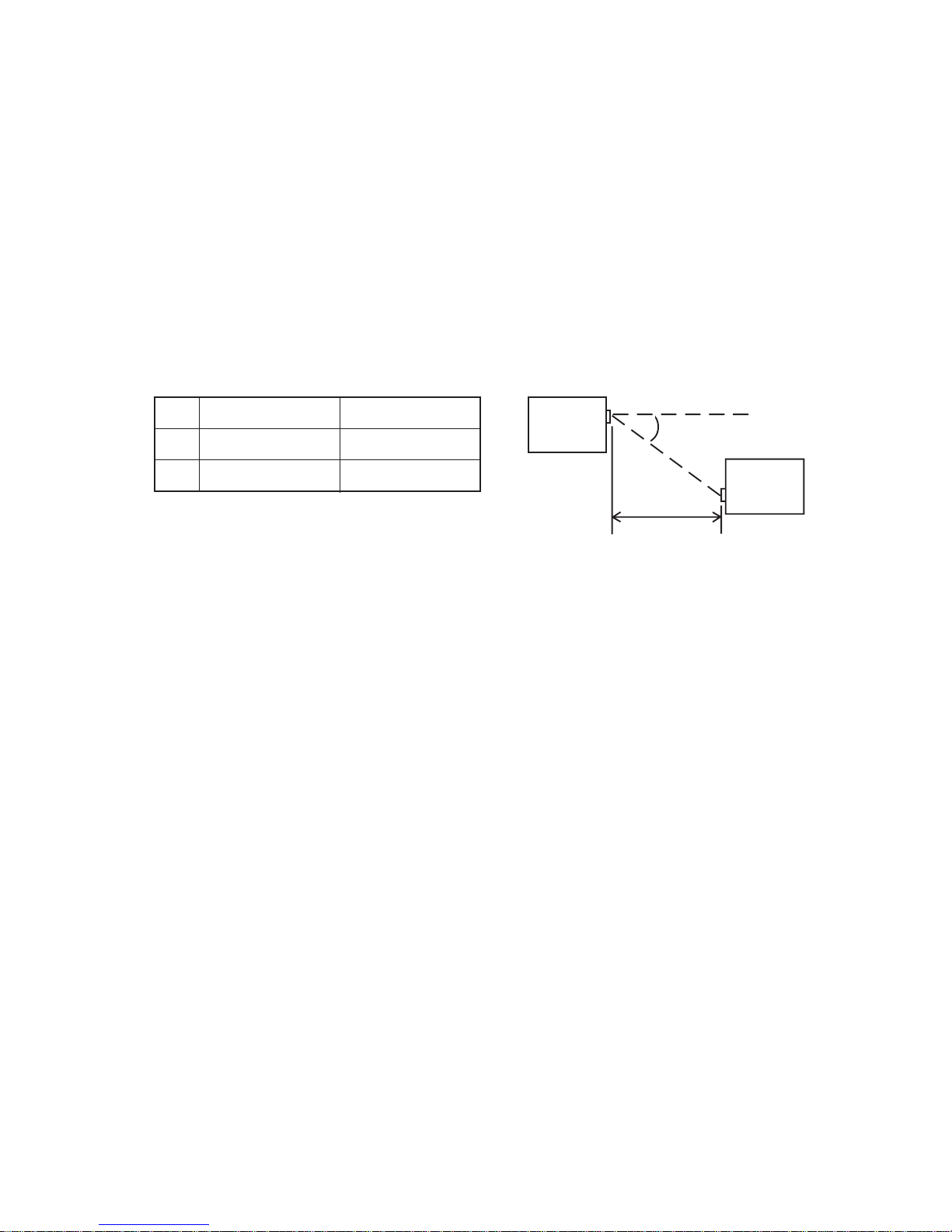
IrDA:
No. Length (L) Angle (A)
1 L = 80 cm A = ±15 degree
2 L = 10 cm A = 0 degree
PA-2400U
A
PA-2400U
L
— 2 —
Page 6
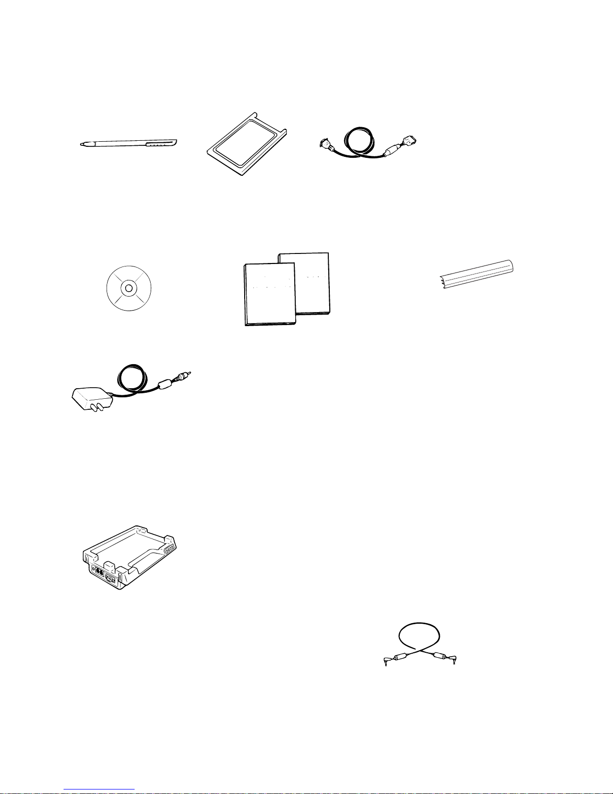
ACCESSORIES
• Stylus • Dummy Card • RS-232C Cable
The stylus is inserted into the CASSIOPEIA.
• CD-ROM
• AC Adapter
*The actual configuration of the AC adapter may differ from that shown in the above illustration.
• Manuals (Hardware Manual, User’s Guide)
The dummy card is inserted in the CASSIOPEIA.
• Rechargeable Battery Pack
(PA-2120L1)
OPTIONS
• I/O BOX PA-2110 IF (MASTER) / I/O BOX PA-2111 IF (SATELLITE)
• Data Communication Cable SB-62
This cable is used to connect a digital camera or other
external equipment to the PA-2400U.
• Dual Battery Charger PA-2040DCHG-E
Note: Optional materials are sold separately.
— 3 —
Page 7
GENERAL GUIDE
• Software Input Panel (SIP) button
Toggles the Software Input Panel on and off. Pressing this button together with the backlight button
displays the calibration screen.
• Backlight button
Toggles the backlight on and off. The
backlight also turns off automatically if
you do not perform any stylus operation
within a certain amount of time. Pressing
this button together with the Software Input Panel button displays the calibration
screen.
• Protective cover
• Data communication connector
For connection of a digital camera
or other peripheral.
• PC card slot cover
• Card eject button
Use this button to eject a PC card from
the unit.
• Speaker/
Microphone
Outputs alarm
and other sounds
and also picks up
sounds for recording.
• Stylus
For performing operations on the
touch screen.
To remove: Pull on the part of the stylus that protrudes from the unit.
To replace: Orient the stylus correctly and slide it into the unit. Press until it clicks into place.
Important
Take care to avoid damaging or losing the stylus.
,
• Power button
Press to toggle power on and off.
• Touch panel
Displays text data and operational indicators.
Keys and icons on the display can be tapped
with the stylus to perform various operations.
— 4 —
Page 8
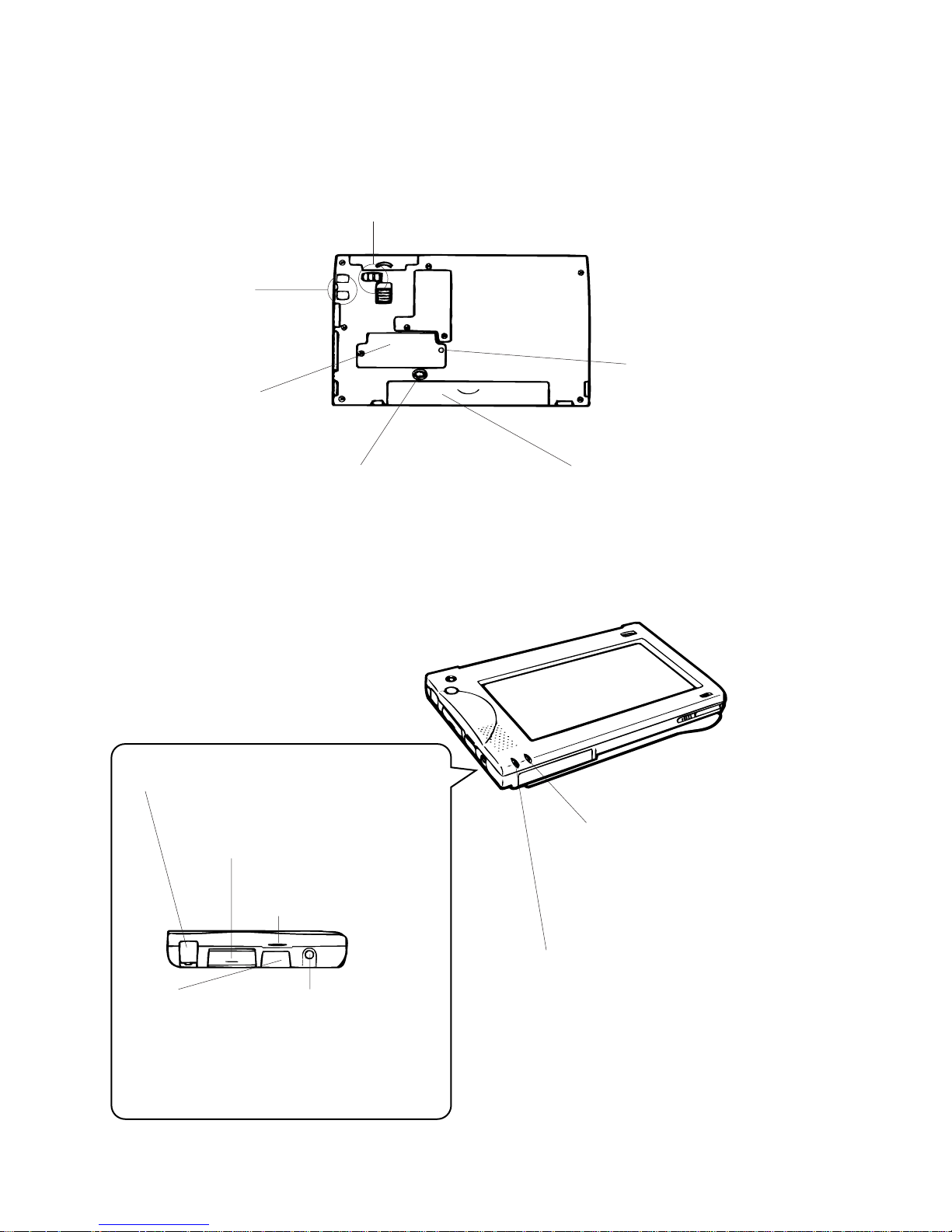
• Charge terminal
Connects to a terminal in
the Interface Unit for
charging.
• Backup battery
compartment cover
Open to access the back-up
battery compartment cover.
• CompactFlash card cover
• CompactFlash card eject lever
• CompactFlash card lock switch
Use the above when installing or removing a CompactFlash card.
• Reset button
See page XX.
• Battery holder release
Slide to release the battery holder.
Make sure this release is in the locked
position whenever using the unit.
• AC adapter connector
For connection of the AC adapter.
• RS-232C connector
For connection of an
RS-232C cable.
• Contrast adjustment dial
Rotate to adjust screen
contrast.
• Battery holder
Holds the main batteries
(two AA-size alkaline).
• Indicator (red)
Lights to indicate an alarm is set.
This indicator is also used to indicate various status of an application.
• Infrared port
• Indicator clear button
Turns off the red indicator
and stops the alarm.
Pressing this button turns
on power. Use the Power
button to turn power off.
• Charge indicator (green)
Lights to indicate that charging is
being performed.
— 5 —
Page 9

DESKTOP COMPUTER SYSTEM CONFIGURATION
The computer configuration described below is required to support the installer and the software applications contained on the Microsoft CD-ROM supplied with the CASSIOPEIA.
• Microsoft Windows NT Workstation 4.0 or Windows 95 (U.S. version)
• Desktop computer with a 486/33DX or higher processor (Pentium P90 recommended)
• 12 MB of memory for Windows NT Workstation 4.0
8 MB of memory (12 MB recommended) for Windows 95
• Hard disk drive with 10 to 50 MB of available hard disk space (actual requirements will vary based on
selection of features and user’s current system configuration)
• Available 9 pin communications port
• One CD-ROM drive
• VGA or higher-resolution graphics card (Super VGA 256-color recommended)
• Keyboard
• Microsoft Mouse or compatible pointing device
Options for either Windows NT Workstation 4.0 or Windows 95:
• Audio card/speakers for sound
• Microsoft Office 97 or Microsoft Office 95
• Serial or built-in infrared adapter for synchronization
• Modem for remote synchronization
• Ethernet LAN connection for remote synchronization
Important
• If you have a notebook PC with IrDA capabilities or a built-in modem, its COM port may not be set up for
use as a standard serial interface. In such a case, you must change the COM port settings so it can be
used as a standard serial interface. You should also check which COM ports are enabled on a desktop
PC before starting to install Windows CE Services. See the documentation that comes with your PC for
details.
— 6 —
Page 10
SETTING UP
1. Load the main batteries.
• Be sure to load the main batteries first. The CASSIOPEIA will not operate properly if you load the backup batteries first.
• Loading the back-up batteries first can cause the battery go dead very quickly. Replace the back-up
battery whenever the low back-up battery warning message appears on the display.
2. Wait for about five seconds and then turn on the CASSIOPEIA.
• Turning on power causes the CASSIOPEIA display to change in the sequence shown below.
Start up
screen
Set up
screens
Set up the CASSIOPEIA as described on page 11 of this manual.
3. After setting up the CASSIOPEIA, turn it off.
4. Load the back-up batteries.
• Use the following procedure to replace the rechargeable back-up battery.
1 Wipe the surface of the rechargeable back-up battery with a soft, dry cloth, and then load it into the
battery compartment with its positive side facing up (so you can see it).
A
2 Replace the battery holder and secure it in place
with Screw A.
3 Replace the sticker.
• See page 9 for details on replacing the primary
battery.
Rdchageable
back-up
battery
Primary
back-up
battery
After completing the above procedure, you can transfer any data you have saved on a disk or other
medium into CASSIOPEIA memory.
Important
• You can also find useful information in the H/PC Companion manual.
• The rechargeable battery pack that comes with the CASSIOPEIA is designed to provide the power
required by the CASSIOPEIA itself, the modem card, and any other devices that require large amounts
of power. It also is the most economical way to power the unit and its peripherals. Because of this, use
of the rechargeable battery pack that comes with the CASSIOPEIA is recommended.
• Should the display lock up or go blank at this time, first perform the full reset (page 12). If this does not
correct the problem, remove the main batteries from the CASSIOPEIA and then remove the back-up
battery. Wait for about five minutes, and then perform this procedure again, starting from step 1. Be
sure that the positive (+) and negative (–) poles of the batteries are facing correctly when you reload
them into the CASSIOPEIA.
• If the message “A problem with memory contents has been found, and memory must be initialized...”
appears, perform the full reset operation described on page 12.
• If the images on the display appear dim, adjust the contrast.
• Further information on the above procedures can be found in the H/PC Companion manual in
the section describing system set up in the owner’s manual.
— 7 —
Page 11
IMPORTANT BATTERY PRECAUTIONS
The CASSIOPEIA has a dual power supply that consists of a battery pack (or ,main batteries) and back-up
batteries. Be sure to load the battery pack (or the main batteries) and back-up batteries before using the
CASSIOPEIA. Also, charge the battery pack (or replace batteries) as soon as possible at the first sign of
low power.
Important!
• Use the battery pack or two AA-size alkaline batteries for the main power supply, and a CR2032 lithium
battery and a IVR 2430 battery for the back-up power supply. Never use any other type of battery with
the CASSIOPEIA.
• The rechargeable back-up battery (IVR2430) is charged by power from the main power supply. The
rechargeable battery is provided in order to prevent premature discharging of the primary back-up battery (CR2032). Never remove the rechargeable back-up battery.
• Never remove both the battery pack (or the main batteries) and the primary back-up battery from the
CASSIOPEIA at the same time. If you do, data stored in memory can be corrupted or lost entirely.
• Never remove the primary back-up battery from the CASSIOPEIA while the battery pack is full discharged (or the main batteries are dead). If you do, data stored in memory can be corrupted or lost
entirely.
• Whenever the battery pack (or the main batteries) and the primary back-up battery both require replacement, be sure to replace the battery pack (or the main batteries) first, before replacing the back-up
battery.
• Be sure to watch out for signs of low battery power. Recharge the battery pack or replace main batteries
as soon as possible after the message shown below appears on the display.
“Your main batteries are running very low on power. Please change the batteries at your next opportunity.”
Replace the primary back-up battery as soon as possible after the message shown below appears.
“Your backup battery is very low or missing. Data loss may result from failure to replace the battery very
soon.”
Failure to replace batteries when they are low can result in corruption or loss of data stored in memory.
Replacing the main batteries
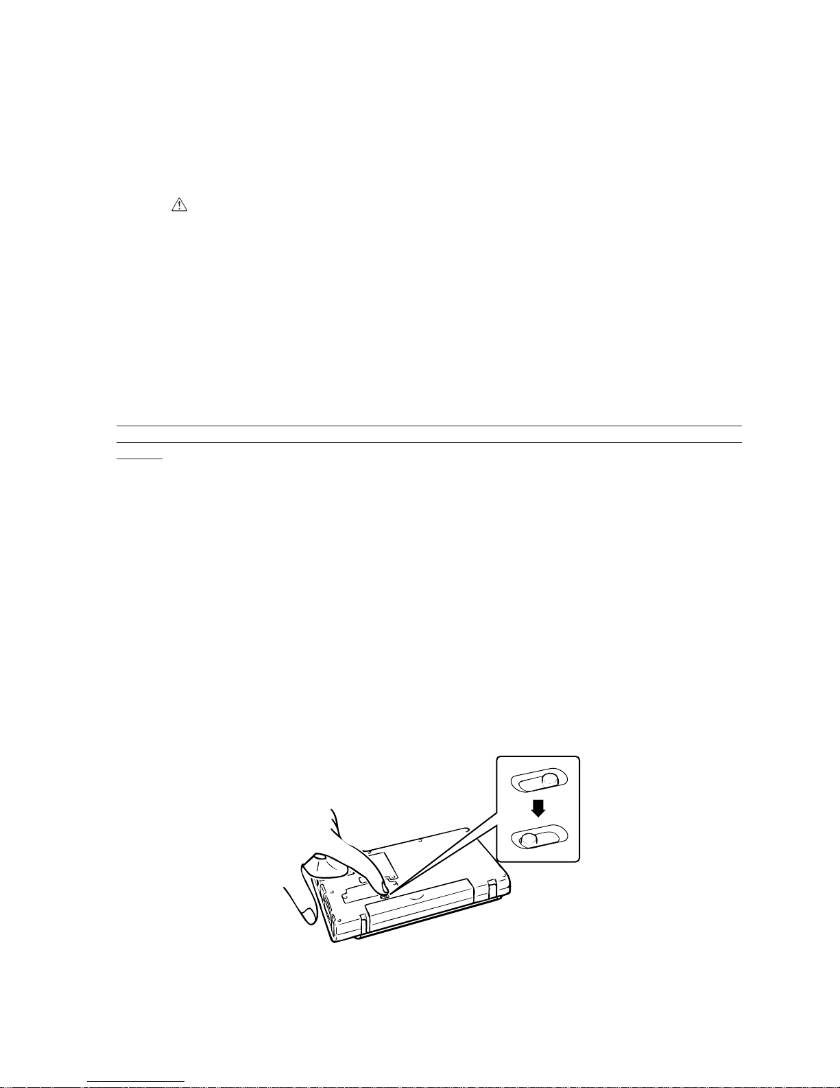
1. Make sure the CASSIOPEIA is turned off.
• If the CASSIOPEIA is on, press the power button to turn it off.
2. Close the CASSIOPEIA and turn it over.
3. While holding the battery holder release in the “FREE” position, slide the battery holder from the CASSIOPEIA.
• While holding the battery holder in release position, grasp the center of the battery holder and carefully
pull it from the CASSIOPEIA.
— 8 —
Page 12
4. Remove the old batteries from the battery holder and load two new ones.
• When loading new batteries, make sure that their positive (+) and negative (–) ends are facing correctly.
5. Reattach the battery holder to the CASSIOPEIA.
• The battery holder will emit a click and the battery holder release will automatically lock when the battery
holder is securely in place.
Replacing the back-up batteries
The CASSIOPEIA uses two lithium batteries for back-up power: a CR2032 primary battery and an IVR2430
rechargeable battery. The rechargeable battery comes pre-installed in the CASIOPEIA when you purchase
it.
Important!
• Never remove both the main batteries and the back-up batteries from the CASSIOPEIA at the same
time. If you do, data stored in memory can be corrupted or lost entirely.
• The rechargeable back-up battery is charged by power from the main batteries. The rechargeable battery is provided in order to prevent premature discharging of the primary back-up battery. Never remove
the rechargeable back-up battery.
• Replace the primary back-up battery as soon as possible after the message shown below appears.
“Your backup battery is very low or missing. Data loss may result from failure to replace the battery very
soon.”
To replace the primary back-up battery
1. Make sure the CASSIOPEIA is turned off.
• If the CASSIOPEIA is on, press the power switch to turn it off.
2. Close the protective cover and turn the CASSIOPEIA over.
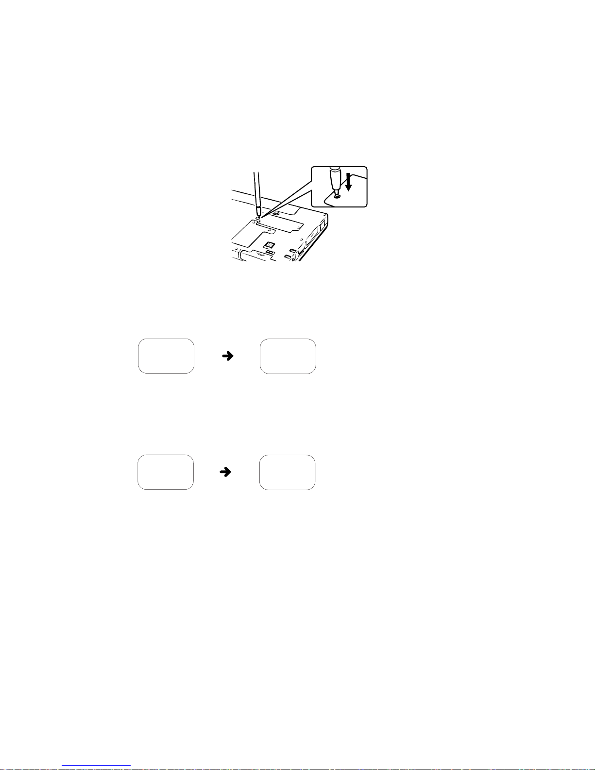
3. Remove the screw that secures the back-up battery compartment cover in place.
— 9 —
Page 13
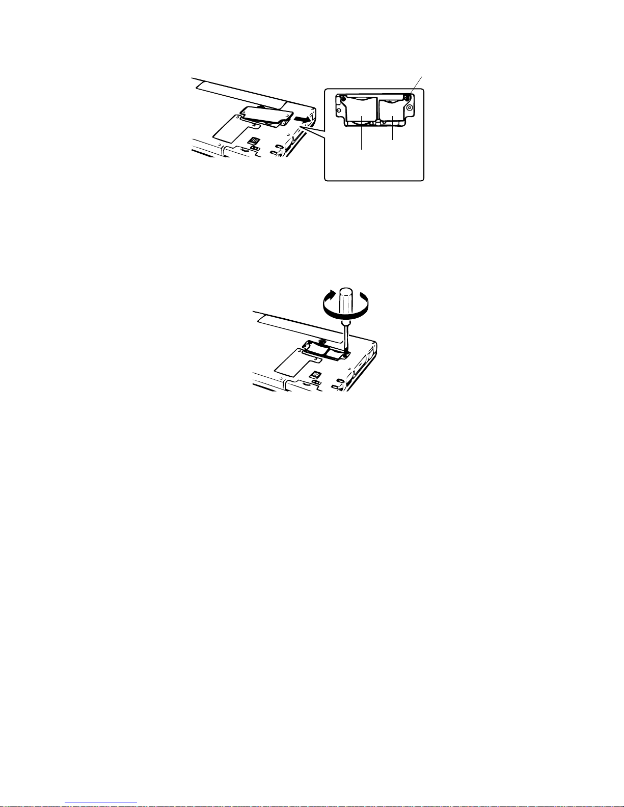
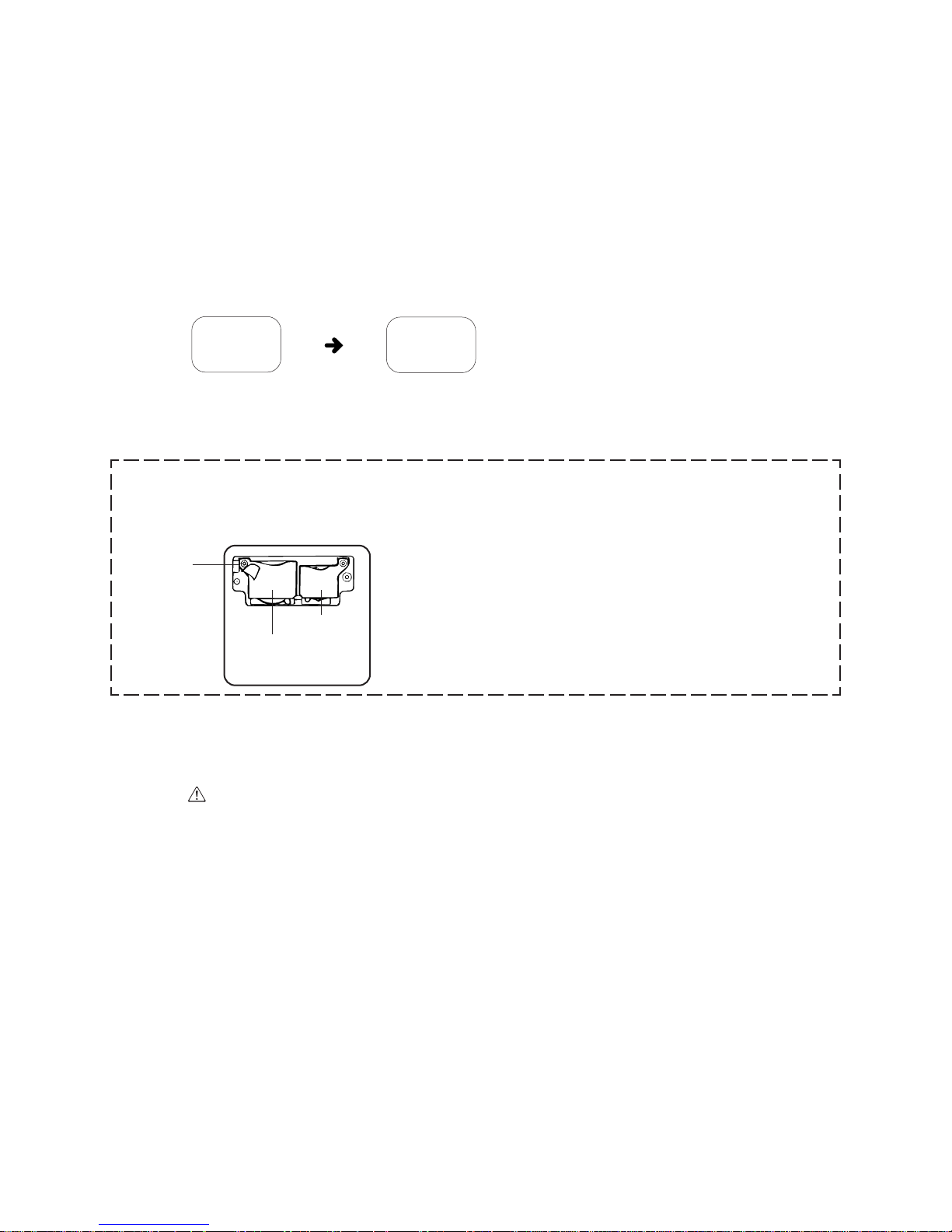
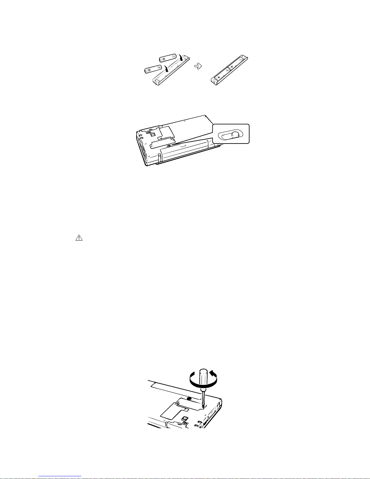
4. Remove the back-up battery compartment cover.
A
Rechargeable
back-up
battery cover
Primary
back-up
battery
cover
5. Remove Screw A and then remove the primary back-up battery holder.
6. Remove the old primary back-up battery.
• Do not remove the rechargeable battery while the primary battery is removed.
7. Wipe off the surfaces of a new lithium battery with a soft, dry cloth and load it into the battery compartment with its positive (+) side facing up (so you can see it).
8. Replace the primary back-up battery holder and secure it in place with its screw.
— 10 —
Page 14
RESET
You should reset the CASSIOPEIA whenever it stops working or whenever some other operational problem
has caused it to malfunction.
To reset the CASSIOPEIA
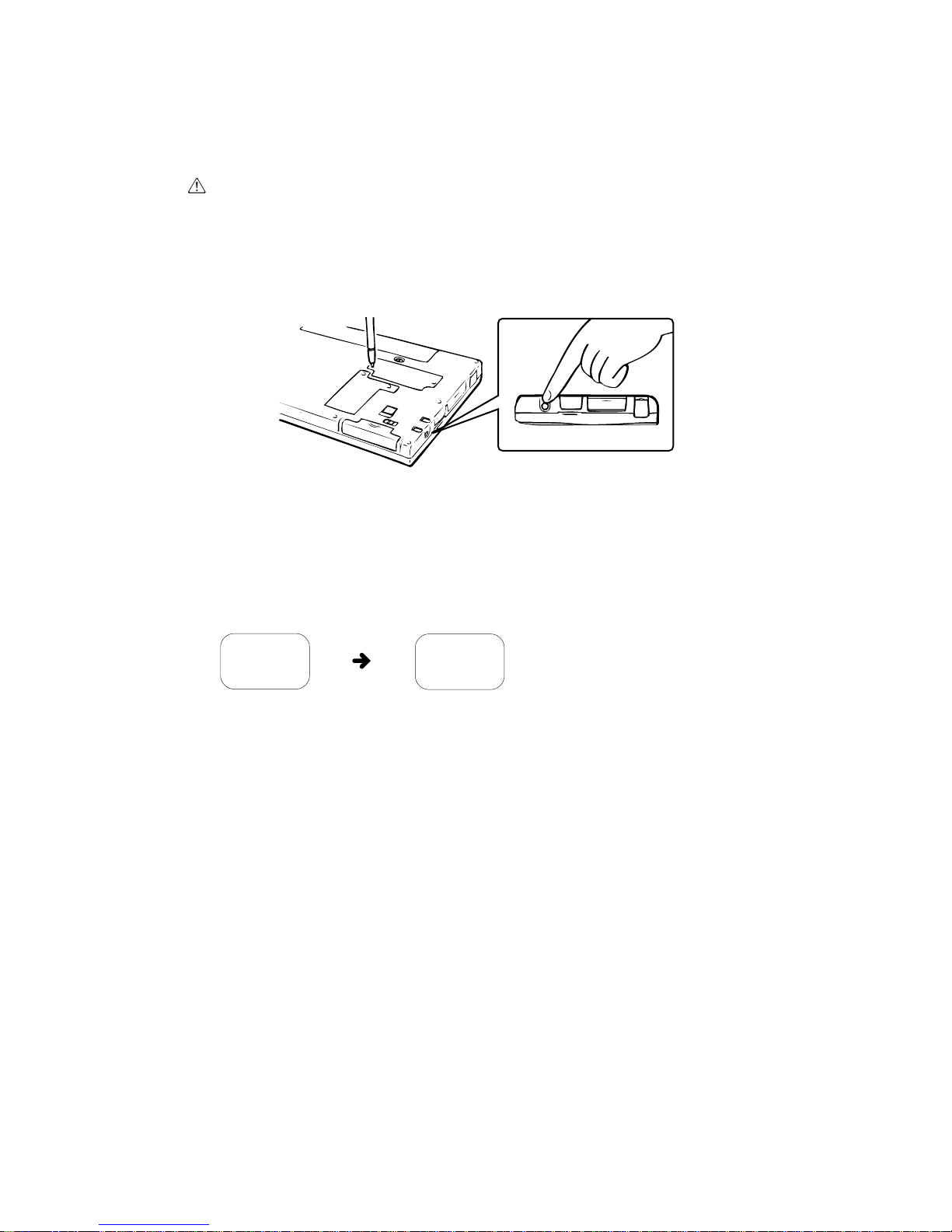
1. Press the RESET button with the stylus.
• This automatically turns off CASSIOPEIA power.
2. Press the power switch to turn on power and start the reset process.
• What happens next depends on memory status.
Case A: Memory Contents Not Corrupted
In this case, the display changes in the sequence shown below.
Start up
screen
Normal operation is restored after the desktop appears, with all memory contents and settings unchanged.
Nomal
Desktop
Case B: Memory Contents Corrupted
In this case, the message “A problem with memory contents has been found, and memory must be initialized...” appears on the screen. Use the stylus to touch the screen to change in the sequence shown below.
Start up
screen
Set up the CASSIOPEIA as described on page 7 of this manual. The desktop appears after set up is
complete.
When memory is seriously corrupted, the above procedure deletes all data stored in memory. When
memory contents are not deleted*, save any data you need onto a computer disk or other medium
and then perform the full reset procedure on page 12.
*Data may be corrupted, so edit data after checking it.
Set up
screens
— 11 —
Page 15
FULL RESET
Perform the full reset when you want to clear all memory contents and settings because memory contents
are corrupted, because you have forgotten the security code, or for any other reason.
Important
The following procedure deletes all data in memory. Be sure to save any important data contents you may
need later to a computer disk or other medium. Always keep separate back-up copies of important data.
To perform a full reset
1. While holding down the indicator clear button, press the RESET button.
2. The message “All memory contents will be deleted! Touch the screen to continue...” appears on the
display.
• If you don’t want to perform a full reset, press the RESET button.
This performs the normal reset, which does not clear memory contents.
\
3. To continue with the full reset procedure and clear all memory contents, touch the screen with the stylus.
• The display changes in the sequence shown below.
Start up
screen
Set up
screens
• Set up the CASSIOPEIA as described on page 7 of this manual.
— 12 —
Page 16
CONNECTING TO A DESKTOP COMPUTER
Use the following procedure to connect the CASSIOPEIA to a desktop computer.
Note that exchanging data with a desktop computer requires Microsoft Windows CE Services, which is on
the Microsoft CD-ROM that is included with the CASSIOPEIA.
Requirements
RS-232C cable (supplied with CASSIOPEIA)
To connect to a desktop computer
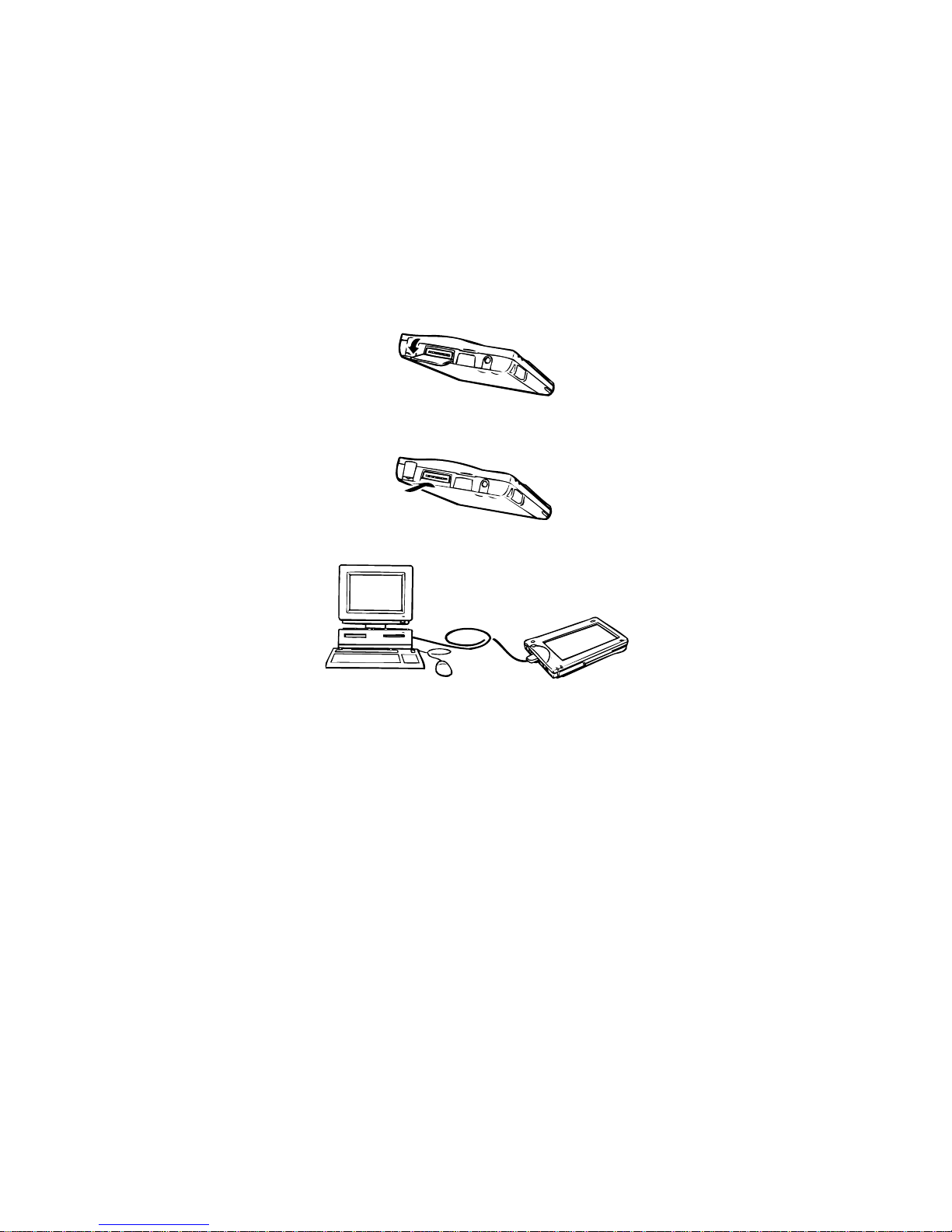
1. Open the RS-232C connector cover on the side of the CASSIOPEIA.
2. Slide the cover into the CASSIOPEIA case as shown below.
3. Use the RS-232C cable to connect the CASSIOPEIA to your desktop computer.
• You can also connect the CASSIOPEIA to your computer using the Interface Unit. See the documentation that comes with the Interface Unit for details.
• If your desktop computer supports infrared communications, you can also use CASSIOPEIA’s infrared
port to exchange data.
— 13 —
Page 17
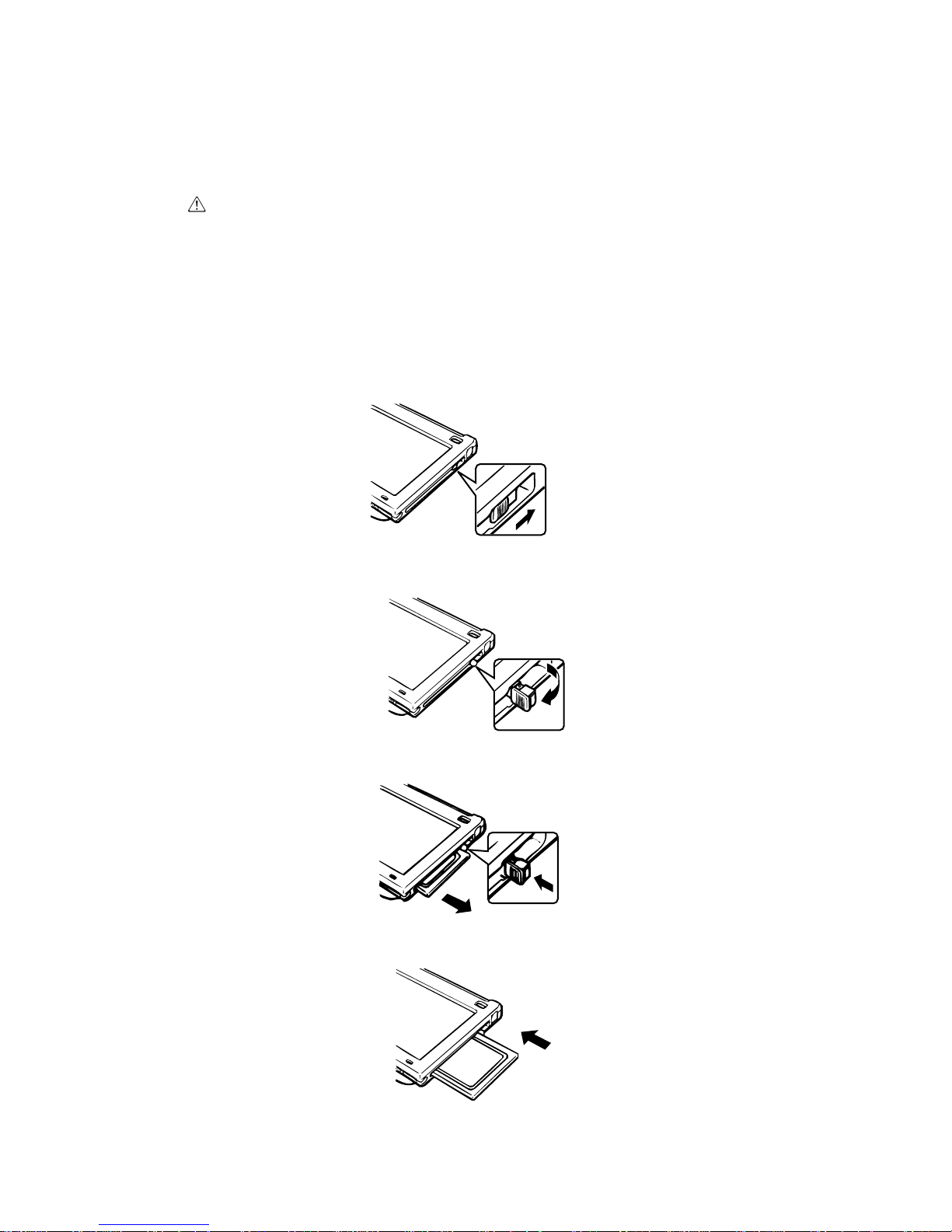
REPLACING THE PC CARD
The CASSIOPEIA comes equipped with a PC card slot that supports memory, modem and other PC cards*.
* Use only PC cards that are compatible with the CASSIOPEIA.
Important
• Be sure to keep the dummy card that comes with the CASSIOPEIA inserted in the card slot whenever
you are not using a PC card.
• Be sure to save any unsaved input or edited data before replacing the PC card.
• Never remove the PC card from the CASSIOPEIA while a PC card operation is in progress. Doing so
can corrupt CASSIOPEIA memory and PC card memory.
To replace the PC card
1. Slide the card lock lever in the direction indicated by the arrow.
2. Raise the card eject button.
3. Use the RS-232C cable to connect the CASSIOPEIA to your desktop computer.
4. Insert a new PC card into the slot.
• Push the card into the slot as far as it will go.
— 14 —
Page 18
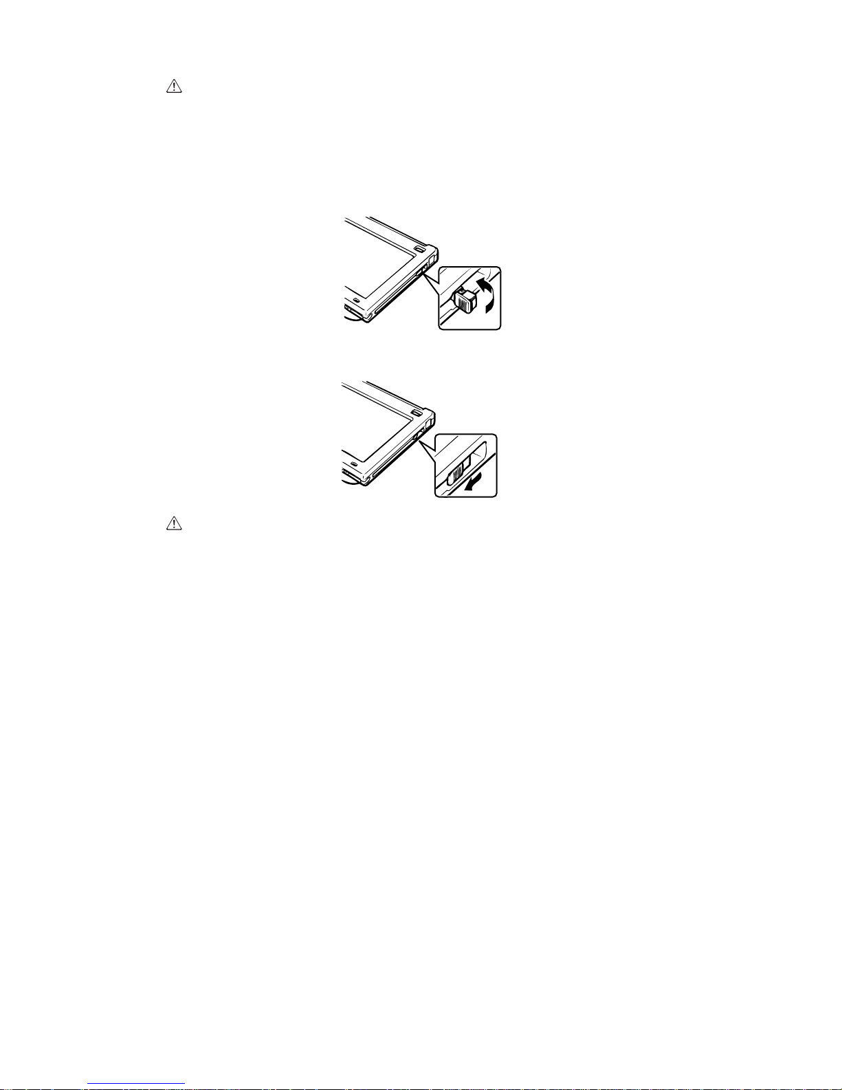
Important
• Take care to orient the card correctly. The top of the card should be facing in the same direction as the
top of the CASSIOPEIA. The card will stop part way into the slot if it is not oriented correctly.
• If the card stops part way into the slot, do not try to force it. Doing so can damage the card or the
CASSIOPEIA. Remove the card, make sure it is oriented correctly, and then try inserting it again.
5. Return the card eject button back to its folded position.
6. Return the card eject button back to its folded position.
Important
• See the documentation that comes with the PC card and the H/PC Companion manual for information
on PC card operations.
• Pressing the Power button to turn off power while a PC card is loaded may cause the enter display
screen to momentarily change to a negative image (black areas become white areas become black).
This dose not indicate malfunction.
— 15 —
Page 19
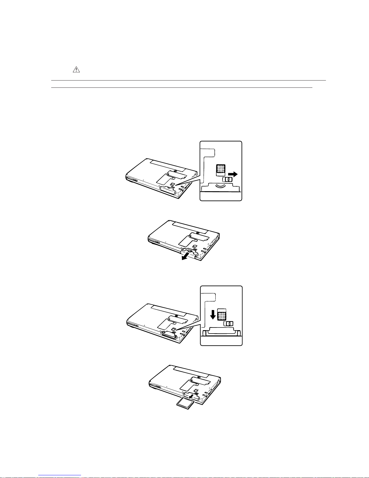
REPLACING THE COMPACTFLASH CARD
The CASSIOPEIA comes equipped with a card slot that supports CompactFlash cards.
Important
• If the card stops part way into the slot, do not try to force it. Doing so can damage the card or the
CASSIOPEIA. Remove the card, make sure it is oriented correctly, and then try inserting it again.
• Be sure to save any unsaved input or edited data before replacing the CompactFlash card.
To replace the CompactFlash card
1. Make sure that CASSIOPEIA power is turned off.
2. Release the card lock switch.
3. Slide the card cover from the CASSIOPEIA.
4. Slide the card eject switch in the direction indicated by the arrow to partially eject the card.
5. Pull the card from the slot.
— 16 —
Page 20
6. Insert a new CompactFlash card into the slot.
• Double-check to make sure that the card is oriented correctly before you insert it into the slot.
• Push the card into the slot as far as it will go.
Important
• Take care to orient the card correctly. The top of the card should be facing in the same direction as the
top of the CASSIOPEIA. The card will stop part way into the slot if it is not oriented correctly.
7. Replace the card cover.
Important
• In order to protect data stored in memory, the CASSIOPEIA automatically turns off whenever you re-
move the card cover. Also, power will not turn on while the cover is removed.
8. Return the card lock switch to its original position.
CONNECTING TO A PRINTER
Use the following procedure to connect the CASSIOPEIA to a printer.
Requirements
• RS-232C cable (supplied with CASSIOPEIA)
• Converter (commercially available)*
* Use a printer or a converter that matches the interface shown on page 18.
To connect to a printer
1. Make sure the printer and the CASSIOPEIA are both turned off.
2. Connect the converter to the connector of the RS-232C cable, and then connect the cable to your printer
and the CASSIOPEIA.
Converter
Connect to printer
RS-232C Cable
• If your printer supports infrared communications, you can also send data using the CASSIOPEIA’s
infrared port.
— 17 —
Page 21
TECHNICAL REFERENCE
About CASSIOPEIA standard interfaces
The following describes the interfaces that are equipped on the CASSIOPEIA as standard.
Basically, operation should not be expected from any device that is not compatible with these interfaces*.
1. Serial Port: Requires a 16550 compatible UART with FIFO buffer.
For RS-232C, Modem, and other connections.
2. Printer Interface: PCL 3 standard. For printers.
* Operation requires development of a separate driver using special development tools.
• Even when using a compatible peripheral, there still may be some minor incompatibilities.
• Some of the modem card models shown on the modem selection screen may not, in fact, be compatible .
• Be sure to read the Microsoft ReadMe file.
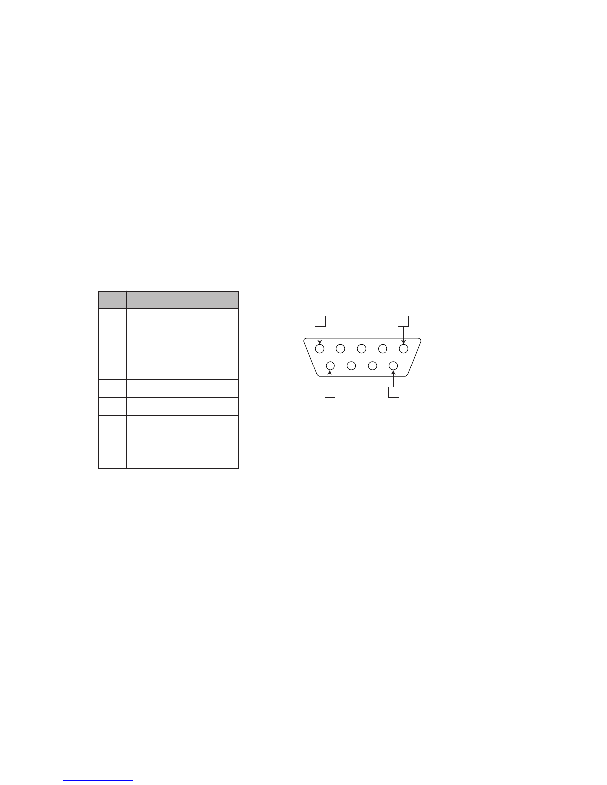
RS-232C interface
Pin Signal Name
1 Data Terminal Ready
2 Transmit Data
3 Receive Data
4 Data Carrier Detect
5 GND
6 Data Terminal Ready
7 Clear To Send
8 Request To Send
9 Reserved
15
69
RS-232C Cable 9-pin Connector
— 18 —
Page 22
MEMORY BACKUP / RESTORE
Make the backup copy by Windows CE Services to your PC before repairing PA-2400U, and restore the
data from PC to user’s PA-2400U after repairing.
For the details of Backup/Restore, refer to the operation manual of Windows CE Services.
Notes: 1* Backup program of Windows CE Services back up only files and databases. Setup data
including Owner, World Clock and so on, can not be backed up to PC.
2* Use AC adaptor when making backup copy and restoring.
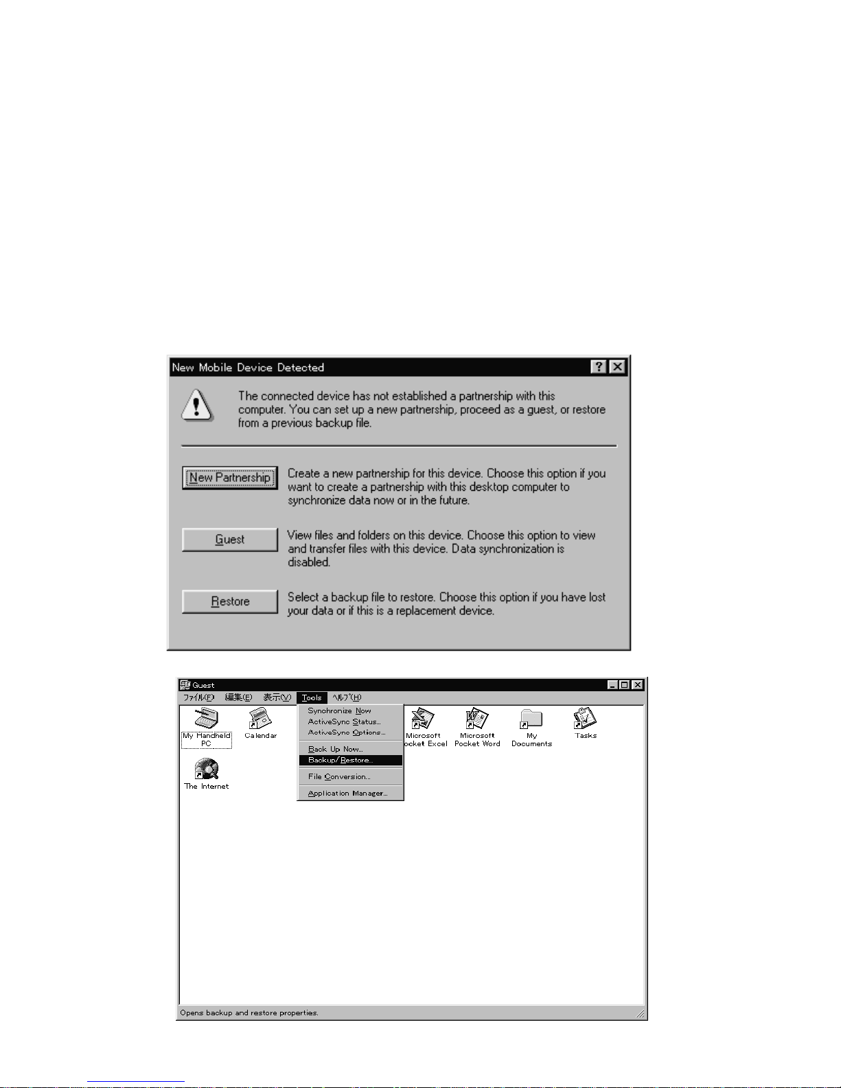
Backup
1. Connect user’s PA-2400U to your PC with RS-232C cable.
2. Start Windows CE Services on your PC.
3. Windows CE Services detects PA-2400U is connected automatically.
4. PC shows the following dialog and click “Guest”.
5. Select “Backup/Restore...” from “Tools” pop up menu.
— 19 —
Page 23
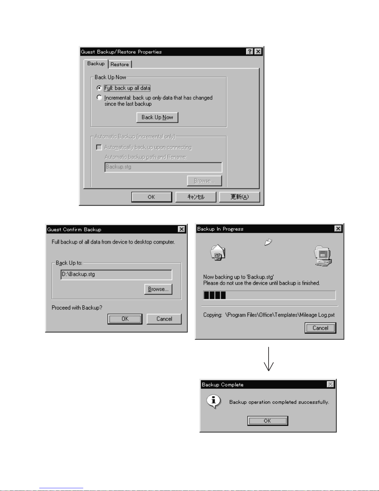
6. Click “Full: back up all data” and “Back Up Now”.
7. Confirm the file name of bakup copy and then click “OK”. Backup starts.
— 20 —
Page 24
Restore
Execute Restore after repairing.
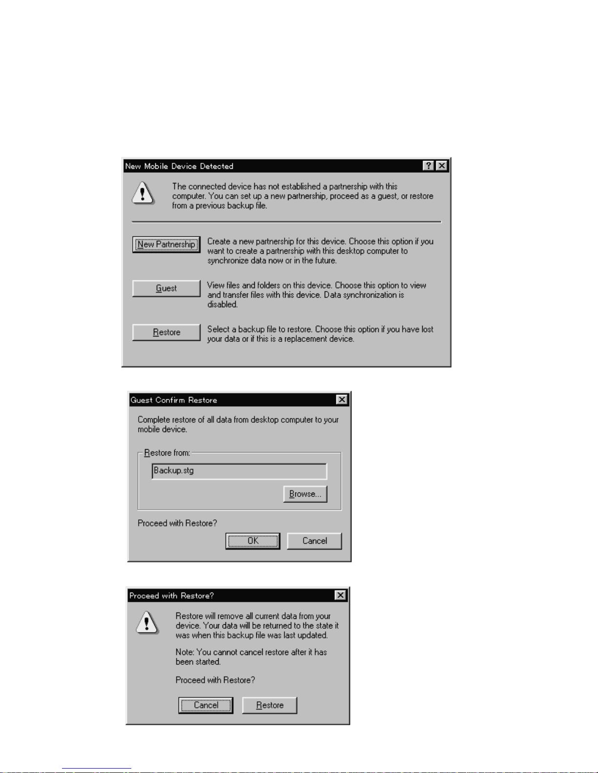
1. Turn on the user’s PA-2400U and then Welcome wizard appears.
2. Execute touch panel calibration and then skip other setups after calibration.
3. Connect repaired PA-2400U to your PC with RS-232C cable.
4. Start Windows CE Services on your PC.
5. Click “Restore” and confirm the file name backed up. Then click “OK”.
6. Click “Restore”.
— 21 —
Page 25
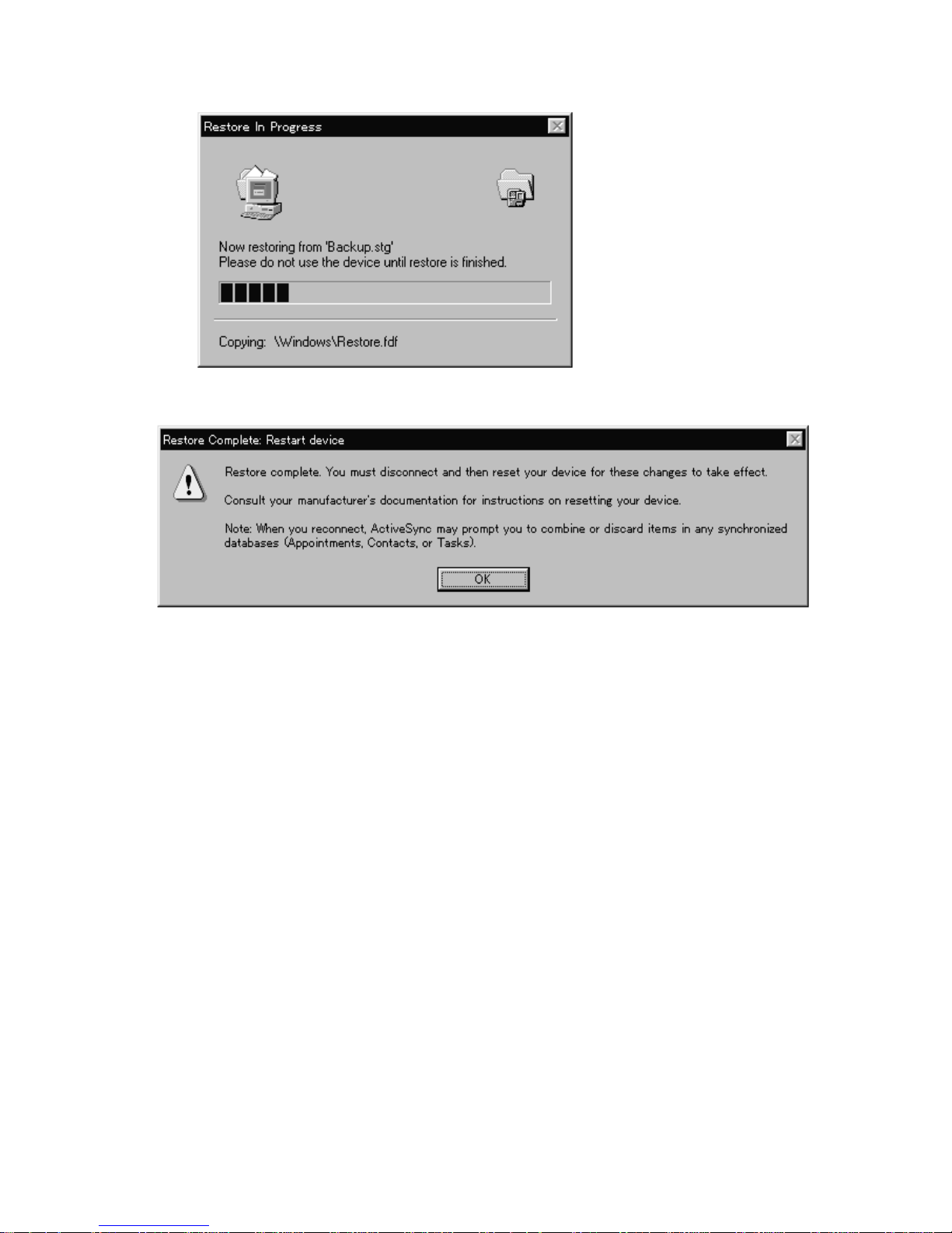
7. Restoring starts.
8. Click “OK”.
— 22 —
Page 26

BLOCK DIAGRAM
CompactFlash
Card
PCMCIA
Card
10 M 32.768 K
PLL X4
80 MHz
CPU
SH-7093 (IC1)
RAM 8 Mbyte
HM51W16160
(RAM1~RAM4)
ROM 16Mbyte
Memory Slot
(MROM1, MROM2)
Audio Amp.
MC34119
(IC9)
SP
Mini Jack
IrDA
IrDA Transceiver
CIM-10S
(IC4)
RS232C
Connector
RS232C Transceiver
MAX3241
(IC5)
+3.3 V +5 V LCD Power
Power Supply
Circuit
Gate Array
MB87A915 (IC3)
ACL
Voltage Detector
Recharger
3.68M
LCD unit
EL
Indicator
(Red) LED
Charge
Indicator
(Green) LED
LCD
EL Driver
HV803
(IC801)
Touch Panel
MIC
AAX2
IVR2430
Alkaline
or
Li-ion
CR2032X2
— 23 —
Page 27

DEVICE FEATURES
Device Features
CPU SH-7093 (IC1)
Hitachi 32 bit RISC CPU.
Sleep/Standby Power Mode.
TLB supports 1K/4K bytes page,128 entries.
8K bytes Cash.
Interrupt Controller.
User Break Controller.
Bus State Controller.
Watch Dog Timer.
CASIO proprietary RTC.
2K bytes Mask ROM.
ON Controller.
1 ch Serial I/F.
1 ch Serial I/F with 16 bytes FIFO.
1 channel Reload Timer.
2 channel Free Run Timer.
System RAM HM51W16160 (RAM1~RAM4)
8M bytes DRAM (16M bit DRAM 4K refresh)
ROM 16M bytes Mask ROM
Memory Slot P660-HROM PCB
Connects to memory board with ROM.
This connects a development board as well.
System LSI MB87A915 (IC3)
LCD Controller.
System Controller.
DRAM Access Controller.
Interrupt Controller.
Key Controller.
Audio Controller.
DMA Controller.
Dead Man’s Switch.
Touch Panel Controller.
Infra Red Controller.
RS232C I/F Controller.
IrDA I/F Controller.
3-pin I/F Controller.
LED Controller.
PCMCIA Controller.
CompactFlash Controller.
LCD 4 gray levels
480 × 240, landscape
0.275 mm/pitch
LCD Driver 2 × 120 ch common driver.
3 × 160 ch segment driver with SRAM and disply control logic.
Touch Panel Resistive input device at the screen pixel resolution.
Just fitting to LCD panel.
Controller in System LSI.
— 24 —
Page 28

Device Features
Touch Panel A/D 10 bit analog to digital converter in System LSI.
Audio D/A 10 bit digital to analog converter in System LSI.
8/11.025/22.05 kHz sampling.
Audio A/D 10 bit analog to digital converter in System LSI.
8/11.025/22.05 kHz sampling.
Speaker 20 mm dynamic type.
PCMCIA One slot for PCMCIA Type I/II card.
Compliance with PCMCIA ver.2.1.
IrDA / RS232C Serial I/F with 16 byte FIFO in CPU.
(alternative) 115.2 kbaud.
IrDA 0 - 1 m.
9-pin RS232C ±12 V I/F.
3-pin Serial Port CASIO proprietary serial interface to Casio’s digital cameras and electric orga-
nizerand so on.
Up to 38.4 kbaud.
0 to +5 V I/F.
Notification LED LED Controller in System LSI.
Notification Button Independent switch.
ACL Automatic hard reset for first time. “Power ON Reset” occurs in case of ACL.
Reset Mechanism ‘Manual Reset’ occurs when user pushes ‘Reset Switch’.
‘Power ON Reset’ occurs when user push ‘Reset Switch’ with pressing ‘Notification Switch’.
Battery Cover Detector Detects both open and closed.
Battery Detector Detects Alkaline or NiMH.
Voltage Detector 5 levels with Alkaline / NiMH and 1 level with backup battery.
Main Battery Alkaline AA × 2.
NiMH.
AC adapter.
Power Supply 3.3 V for most hardware logic.
5 V for PCMCIA and 3-pin serial interface.
24 V for LCD panel driver.
— 25 —
Page 29

LSI/IC DATA
SH-7093 (CPU / IC1)
No. Pin Name In/Out Function To/From
1 D27 I/O Data bus
2 D26 I/O Data bus
3 D25 I/O Data bus
4 D24 I/O Data bus
5 D23/Port 7 I/O Data bus
6 Vss GND
7 Vcc +3.3V source
8 D22/Port 6 I/O Data bus
9 D21/Port 5 I/O Data bus
10 D20/Port 4 I/O Data bus
11 D19/Port 3 I/O Data bus
12 D18/Port 2 I/O Data bus
13 D17/Port 1 I/O Data bus
14 D16/Port 0 I/O Data bus
15 D15 I/O Data bus
16 D14 I/O Data bus
17 Vss GND
18 Vcc +3.3V source
19 Vss GND
20 Vcc +3.3V source
21 D13 I/O Data bus
22 D12 I/O Data bus
23 D11 I/O Data bus
24 D10 I/O Data bus
25 D9 I/O Data bus
26 D8 I/O Data bus
27 D7 I/O Data bus
28 D6 I/O Data bus
29 D5 I/O Data bus
30 Vss GND
31 Vcc +3.3V source
32 D4 I/O Data bus
33 D3 I/O Data bus
34 D2 I/O Data bus
35 D1 I/O Data bus
36 D0 I/O Data bus
37 A0 O Address bus
38 A1 O Address bus
39 A2 O Address bus
40 A3 O Address bus
41 Vss GND
42 Vcc +3.3V source
43 A4 O Address bus
44 A5 O Address bus
45 A6 O Address bus
46 A7 O Address bus
47 A8 O Address bus
48 A9 O Address bus
49 Vss GND
50 Vcc +3.3V source
51 A10 O Address bus
52 A11 O Address bus
53 A12 O Address bus
54 Vss GND
55 Vcc +3.3V source
56 A13 O Address bus
57 A14 O Address bus
— 26 —
Page 30

No. Pin Name In/Out Function To/From
g
58 A15 O Address bus
59 Vss GND
60 Vcc +3.3V source
61 A16 O Address bus
62 A17 O Address bus
63 A18 O Address bus
64 A19 O Address bus
65 A20 O Address bus
66 A21 O Address bus
67 A22 O Address bus
68 Vss GND
69 Vcc +3.3V source
70 A23 O Address bus
71 A24 O Address bus
72 A25 O Address bus
73 Vss (PLL) GND for PLL
74 CAP1 O Capacitor connecting terminal for PLL
75 Vcc (PLL)
+3.3V source for PLL
76 Vss GND
77 ONENB I ON Circuit enable signal BGA288
78 Vcc +3.3V source
79 EXTAL I Oscillator in (10MHz) X2
80 XTAL O Oscillator out (10MHz) X2
81 TESTMDB I Test mode control GND
82 Vss GND
83 Vcc +3.3V source
84 MD2 / RXD0 I Data input of serial port 0 BGA288
85 MD1 / TXD0 I/O Data output of serial port 0 BGA288
86 MD0 / SCK0 I/O Not used
87 BREQB I Bus request BGA288
88 RESETB I Reset signal from BGA288 BGA288
89 NMI I Non-maskable Interrupt request BGA288
90 IRL3B I Interrupt request BGA288
91 RXD1 I Data input of serial port 1 IC5(RS232C),BGA288
92 TXD1 O Data output of serial port 1 IC5(RS232C),BGA288
93 SCK1 I/O Clock of serial port 1 BGA288
94 CTS1 I Serial port 1 transmission permission IC5(RS232C)
95 RTS1 O Serial port 1 transmission request IC5(RS232C)
96 BACKB O Bus access permission BGA288
97 IOIS16B I Write protect input BGA288
98 STATUS0 O
STATUS0 si
nal to BGA288
BGA288
99 ONSTATUSB O V3ROM (+3.3V) ON/OFF control. H=ON BGA288,Power supply unit
100 Vss GND
101 CKIO I/O System clock I/O BGA288
102 Vcc +3.3V source
103 MD4 / CE2BB I/O PCMCIA CE2B signal BGA288
104 MD3 / CE2AB I/O PCMCIA CE2A signal BGA288
105 ONB I On circuit start request BGA288
106 RD / WRB O Read/Write signal BGA288,RAM,ROM
107 RDB O Read pulse BGA288,ROM,LCD unit
108 CS6B / CE1BB O Chip select-6 sigmal BGA288
109 CS5B / CE1AB O Chip select-5 sigmal BGA288
110 CS4B O Chip select-4 sigmal BGA288,ROM Board
111 CS3B O Not used
112 CS2B O Chip select-2 sigmal BGA288
113 CS1B O Chip select-1 sigmal ROM Board
114 CS0B O Chip select-0 sigmal ROM Board
115 Vss GND
116 Vcc +3.3V source
117 WE3B / ICIOWRB O D31-D24 select signal / IO Write BGA288
118 WE2B / ICIORDB O D23-D16 select signal / IO Read BGA288,ROM Board
— 27 —
Page 31

No. Pin Name In/Out Function To/From
119 CASHHB / CAS2HB O D31-D24 / D15-D8 select signal BGA288,ROM Board
120 CASHLB / CAS2LB O D23-D16 / D7-D0 select signal BGA288,ROM Board
121 Vss GND
122 Vcc +3.3V source
123 WE1B O D15-D8 select signal BGA288
124 WE0B O D7-D0 select signal BGA288,LCD uint,ROM Board
125 CASLHB O D15-D8 select signal BGA288,ROM Board
126 CASLLB / OEB O D7-D0 select / memory select signal BGA288,ROM Board
127 Vss GND
128 Vcc +3.3V source
129 RASB / CEB O CE signal for RAM,ROM BGA288,RAM,ROM Board
130 MD5 / RAS2B Not used
131 HSTBYB I Not used +3.3V source
132 WAITB I Hardware wait request BGA288
133 Vss GND
134 RTCCLK O RTC clock output BGA288
135 Vcc(RTC) +3.3V source(for internal RTC)
136 XTAL2 O Oscillator terminal(for internal RTC) C6
137 EXTAL2 I Oscillator terminal(for internal RTC) C6
138 Vss(RTC) GND(for internal RTC)
139 Vcc +3.3V source
140 D31 I/O Data bus
141 D30 I/O Data bus
142 D29 I/O Data bus
143 D28 I/O Data bus
144 Vss GND
— 28 —
Page 32

MB87A915 (Gate Array/IC3)
y
No. Pin Name Volt In/Out Function To/From
1 CFCE1B 3v O CE signal for CompactFlash card CompactFlash card
2 IOPORT0 3v I Detects I/O BOX Q131 (Power supply)
3 IOPORT1 3v I/O I/O Port 1 LCD unit
4 VSS GND
5 V5D3 5V I/O Data bus PCMCIA CARD
6 VS1 Voltage detect for PCMCIA PCMCIA CARD
7 V5D4 5V I/O Data bus PCMCIA CARD
8 V5D11 5V I/O Data bus PCMCIA CARD
9 CD1B I PCMCIA CARD detect PCMCIA CARD
10 V5D5 5V I/O Data bus PCMCIA CARD
11 VDD1 5V +5V source
12 V5CE2B 5V O CE2 signal for PCMCIA CARD PCMCIA CARD
13 V5D12 5V I/O Data bus PCMCIA CARD
14 V5D6 5V I/O Data bus PCMCIA CARD
15 V5D13 5V I/O Data bus PCMCIA CARD
16 V5CE1B 5V O CE1 signal for PCMCIA CARD PCMCIA CARD
17 V5A10 5V O Address bus PCMCIA CARD
18 V5OEB 5V O OE signal for PCMCIA CARD PCMCIA CARD
19 V5A11 5V O Address bus PCMCIA CARD
20 VSS GND
21 VDD1 5V +5V source
22 VSS GND
23 V5IORDB 5V O IORD signal for PCMCIA CARD PCMCIA CARD
24 V5A9 5V O Address bus PCMCIA CARD
25 V5IOWRB 5V O IOWR signal for PCMCIA CARD PCMCIA CARD
26 V5A8 5V O Address bus PCMCIA CARD
27 V5A17 5V O Address bus PCMCIA CARD
28 V5A13 5V O Address bus PCMCIA CARD
29 V5A18 5V O Address bus PCMCIA CARD
30 V5A14 5V O Address bus PCMCIA CARD
31 VDD1 5V +5V source
32 V5A19 5V O Address bus PCMCIA CARD
33 V5WEB 5V O WE signal for PCMCIA CARD PCMCIA CARD
34 V5A20 5V O Address bus PCMCIA CARD
35 V5A21 5V O Address bus PCMCIA CARD
36 V5A16 5V O Address bus PCMCIA CARD
37 VSS GND
38 V5A22 5V O Address bus PCMCIA CARD
39 V5A15 5V O Address bus PCMCIA CARD
40 VDD1 5V +5V source
41 V5A23 5V O Address bus PCMCIA CARD
42 V5A12 5V O Address bus PCMCIA CARD
43 V5A24 5V O Address bus PCMCIA CARD
44 V5A7 5V O Address bus PCMCIA CARD
45 VDD1 5V +5V source
46 VSS GND
47 V5A25 5V O Address bus PCMCIA CARD
48 V5A6 5V O Address bus PCMCIA CARD
49 V5A5 5V O Address bus PCMCIA CARD
50 V5RESET 5V O Reset signal for PCMCIA CARD PCMCIA CARD
51 V5A4 5V O Address bus PCMCIA CARD
52 V5A3 5V O Address bus PCMCIA CARD
53 V5A2 5V O Address bus PCMCIA CARD
54 V5REGB 5V O
55 VDD1 5V +5V source
56 V5D7 5V I/O Data bus PCMCIA CARD
57 V5D14 5V I/O Data bus PCMCIA CARD
58 V5A1 5V O Address bus PCMCIA CARD
59 V5D15 5V I/O Data bus PCMCIA CARD
Attribute memor
select
PCMCIA CARD
— 29 —
Page 33

No. Pin Name Volt In/Out Function To/From
60 V5D0 5V I/O Data bus PCMCIA CARD
61 V5A0 5V O Address bus PCMCIA CARD
62 VDD1 5V +5V source
63 V5D8 5V I/O Data bus PCMCIA CARD
64 V5D1 5V I/O Data bus PCMCIA CARD
65 V5D9 5V I/O Data bus PCMCIA CARD
66 V5BSYB 5V I Busy/Ready signal for PCMCIA CARD PCMCIA CARD
67 VSS GND
68 VSS GND
69 V5WAITB 5V I Wait signal for PCMCIA CARD PCMCIA CARD
70 V5D2 5V I/O Data bus PCMCIA CARD
71 V5INPACKB 5V I Input response PCMCIA CARD
72 V5D10 5V I/O Data bus PCMCIA CARD
73 V5BVD2 5V I Voltage detect for PCMCIA PCMCIA CARD,SP
74 LEDONB 3V O LED signal LCD unit
75 PIRB 3V O Voltage V5IRDA(3V) control Q123(Power)
76 V5BVD1 5V I Battery Detector PCMCIA CARD
77 V5IOIS16B 5V I Write protect PCMCIA CARD
78 IRTXD 3V O Infrared output IrDA
79 CD2B 3V I Card detect PCMCIA CARD
80 IRRXD 3V I Infrared input IrDA
81 VDD2 3V +3V source
82 VSS GND
83 DISPOFFB 3V O LCD off signal LCD unit
84 DISPCSB 3V O CE signal for LCD driver LCD unit
85 DISPRSTB 3V O Reset signal for LCD driner LCD unit
86 DISPWTB 3V I Wait signal from LCD driver LCD unit
87 IOPORT2 3V I/O Not used
88 PSW0 3V O Touch panel control Touch panel
89 PSW1 3V O Touch panel control Touch panel
90 PSW2 3V O Touch panel control Touch panel
91 PSW3 3V O Touch panel control Touch panel
92 PSW4 3V O Touch panel control Touch panel
93 FLSHRSTB 3V O Reset signal for Flash ROM board
94 PMUTE 3V O Audio mute signal Audio amp
95 PRECB 3V O Power supply control for recording circuit LCD unit
96 FUNKEYIN7 3V I Function input Keyboard
97 FUNKEYIN6 3V I Function input Keyboard
98 FUNKEYIN5 3V I Function input Keyboard
99 FUNKEYIN4 3V I Function input Keyboard
100 FUNKEYIN3 3V I Function input Keyboard
101 FUNKEYIN2 3V I Function input Keyboard
102 FUNKEYIN1 3V I Function input Keyboard
103 NC Not used
104 AVCC3 Analog I +3V source for D/A converter of audio +3V source
105 AUDIN Analog I Audio signal input for record LCD unit
106 AUDVRL Analog I Reference voltage for A/D,D/A converters
107 AUDOUT Analog O Audio signal output for play Audio amp
108 AUDVRH Analog I Reference voltage for A/D,D/A converters
109 AVCC2 Analog I +3V source for Touch panel +3V source
110 AGND2 Analog I Ground for Touch panel GND
111 AGND1 Analog I Analog ground GND
112 AVCC1 Analog I +3V source for D/A converter of audio +3V source
113 TCPIN2 Analog I Analog signal input from Touch panel Touch panel
114 VDETADIN Analog I Power detecting signal Power supply
115 TCPVRL Analog I Reference voltage for A/D converter of TP
116 TCPVRH Analog I Reference voltage for A/D converter of TP
117 TCPIN1 Analog I Analog signal input from Touch panel Touch panel
118 NC Not used
119 FUNKEYIN0 3V I Function input Keyboard
120 KBOUT8 3V O Key common signal Keyboard
— 30 —
Page 34

No. Pin Name Volt In/Out Function To/From
121 KBOUT7 3V O Key common signal Keyboard
122 KBOUT6 3V O Key common signal Keyboard
123 KBOUT5 3V O Key common signal Keyboard
124 KBOUT4 3V O Key common signal Keyboard
125 KBOUT3 3V O Key common signal Keyboard
126 KBOUT2 3V O Key common signal Keyboard
127 KBOUT1 3V O Key common signal Keyboard
128 KBOUT0 3V O Key common signal Keyboard
129 KBDIN0 3V I Key input signal Keyboard
130 KBDIN1 3V I Key input signal Keyboard
131 KBDIN2 3V I Key input signal Keyboard
132 KBDIN3 3V I Key input signal Keyboard
133 KBDIN4 3V I Key input signal Keyboard
134 KBDIN5 3V I Key input signal Keyboard
135 KBDIN6 3V I Key input signal Keyboard
136 VSS GND
137 KBDIN7 3V I Key input signal Keyboard
138 XCKIN Analog I Oscillator input(3.68MHz) X1
139 XCKOUT Analog I/O Oscillator output(3.68MHz) X1
140 VDD2 3V +3V source
141 ONSWB 3V I ON switch signal Keyboard
142 PENPUTB 3V I Pen down status signal Touch panel
143 LEDOFFB 3V I LED cancel signal LCD unit (SW)
144 DOCKB 3V I Cradle detector RS232C
145 CHGDTCT 3V I Power supply
146 ACLB 3V I ACL signal at battery loaded. IC113(Power supply)
147 BCVRB 3V I Battery cover detecting port SW100
148 BATDTCT 3V I Alkaline/NiMH detecting port SW101
149 ACDTCTB 3V I AC adaptor detect port Q105 (Power supply)
150 VDETS 3V I Backup battery detecting signal Q119 (Power supply)
151 VDTC5B 3V I Alkaline battery detecting signal IC109 (Power supply)
152 VDTC3B 3V I Alkaline battery detecting signal IC110 (Power supply)
153 VDET3B 3V I Alkaline battery detecting signal IC107 (Power supply)
154 VDET2R 3V I NiMH detecting signal(Off) Q100 (Power supply)
155 VDET2 3V I Alkaline battery detecting signal(Off) Q103 (Power supply)
156 VDET1RB 3V I NiMH detecting signal(Low Battery) IC101 (Power supply)
157 VDET1B 3V I Alkaline battery detecting signal(Low Battery) IC100 (Power supply)
158 PSEL5 3V O Power supply select signal for PCMCIA (3/5V) Q113 (Power supply)
159 PLCD 3V O LCD Voltage control signal Q201 (I/F Block)
160 PEL 3V O EL Voltage control signal Q116 (Power supply)
161 PDMMYS 3V O For backup battery detector IC115 (Power supply)
162 PDMMYM 3V O V3 system control signal Q112 (Power supply)
163 PCRD2 3V O VGA288 Voltage control signal Q118 (Power supply)
164 PCRD 3V O PCMCIA Voltage control signal Q117 (Power supply)
165 P5DCHG 3V O V5 Voltage control signal Q115 (Power supply)
166 P5V 3V O V5 Voltage control signal Q107,Q111 (Power supply)
167 P25ON 3V O LCD(+25V) Voltage control signal IC201
168 EVOLDAT 3V O Electronic volume (DAT) IC202 (EVOL)
169 EVOLDIR 3V O Electronic volume (DIR) IC202 (EVOL)
170 EVOLCS 3V O Electronic volume (CS) IC202 (EVOL)
171 EVOLCLK 3V O Electronic volume (CLK) IC202 (EVOL)
172 CAS1HUB 3V O CAS signal for DRAM DRAM
173 CAS1HLB 3V O CAS signal for DRAM DRAM
174 CAS1LUB 3V O CAS signal for DRAM DRAM
175 CAS1LLB 3V O CAS signal for DRAM DRAM
176 CAS0HUB 3V O CAS signal for DRAM DRAM
177 CAS0HLB 3V O CAS signal for DRAM DRAM
178 CAS0LUB 3V O CAS signal for DRAM DRAM
179 VSS GND
180 VDD2 3V +3V source
181 CAS0LLB 3V O CAS signal for DRAM DRAM
— 31 —
Page 35

No. Pin Name Volt In/Out Function To/From
182 LOCK 3V I Not used
183 MEMCLB 3V I Not used
184 A25 3V I Address bus
185 A24 3V I Address bus
186 A23 3V I/O Address bus
187 A22 3V I/O Address bus
188 A21 3V I/O Address bus
189 A20 3V I/O Address bus
190 A19 3V I Address bus
191 A18 3V I Address bus
192 A17 3V I Address bus
193 A16 3V I Address bus
194 A15 3V I Address bus
195 A14 3V I Address bus
196 A13 3V I Address bus
197 A12 3V I Address bus
198 A11 3V I/O Address bus
199 A10 3V I/O Address bus
200 A9 3V I/O Address bus
201 A8 3V I/O Address bus
202 A7 3V I/O Address bus
203 VSS GND
204 A6 3V I/O Address bus
205 A5 3V I/O Address bus
206 A4 3V I/O Address bus
207 VDD2 3V +3V source
208 A3 3V I/O Address bus
209 A2 3V I/O Address bus
210 A1 3V I Address bus
211 A0 3V I Address bus
212 D0 3V I/O Data bus
213 D1 3V I/O Data bus
214 D2 3V I/O Data bus
215 D3 3V I/O Data bus
216 D4 3V I/O Data bus
217 D5 3V I/O Data bus
218 VDD2 3V +3V source
219 VSS GND
220 D6 3V I/O Data bus
221 D7 3V I/O Data bus
222 D8 3V I/O Data bus
223 D9 3V I/O Data bus
224 D10 3V I/O Data bus
225 D11 3V I/O Data bus
226 D12 3V I/O Data bus
227 D13 3V I/O Data bus
228 D14 3V I/O Data bus
229 D15 3V I/O Data bus
230 MCLOCK 3V I CKIO signal from CPU IC1
231 ONENB 3V O ON Circuit enable signal IC1
232 RXD0 3V O Data output of serial port 0 IC1
233 TXD0 3V I Data input of serial port 0 IC1
234 BREQB 3V O REQ signal to CPU IC1
235 RESETB 3V O RESET signal to CPU IC1
236 VSS GND
237 IRQB 3V O IRQ signal to CPU IC1
238 RXDSH 3V I/O Data output of signal port 1 IC5(RS232C),BGA288
239 TXDSH 3V I Data input of serial port 1 BGA288
240 SCK 3V O Clock of serial port 1 IC1
241 BACKB 3V I Bus access permission from CPU IC1
242 IOIS16B 3V O Write protect signal to CPU IC1
— 32 —
Page 36

No. Pin Name Volt In/Out Function To/From
g
243 STATUS0 3V I
STATUS0 si
nal from CPU
IC1
244 ONSTATUSB 3V I ONSTATUS signal from CPU IC1
245 CE2B 3V I CE2B signal from CPU IC1
246 CE2A 3V I CE2A signal from CPU IC1
247 VDD2 3V +3V source
248 ONB 3V O ON circuit start signal to CPU IC1
249 RDWRB 3V I/O Read/Write signal from CPU IC1
250 RDB 3V I Read pulse signal from CPU IC1
251 CS6B 3V I Chip select-6 signal from CPU (PCMCIA) IC1
252 CS4B 3V I Chip select-4 signal from CPU (HOTARU) IC1
253 CS2B 3V I Chip select-2 signal from CPU (LCD Driver) IC1
254 CS5B 3V I Chip select-5 signal from CPU IC1
255 ICIOWRB 3V I IOWR signal from CPU IC1
256 ICIORDB 3V I IORD signal from CPU IC1
257 CASHHB 3V I CASHH signal from CPU IC1
258 CASHLB 3V I CASHL signal from CPU IC1
259 WRHB 3V I WE1 signal from CPU IC1
260 WRLB 3V I WE0 signal from CPU IC1
261 CASLHB 3V I CASLH signal from CPU IC1
262 CASLLB 3V I CASLL signal from CPU IC1
263 RASB 3V I/O RAS/CE signal from CPU IC1
264 HSTBY 3V O HSTBY signal to CPU IC1
265 WAITB 3V O WAIT signal to CPU IC1
266 CKRTC256 3V I RTC clock signal from CPU IC1
267 CFCVRB 3V I Compact Flash lock switch SW1
268 CFWEB 3V O WE signal for CompactFlash card CompactFlash card
269 CFWAITB 3V I Wait signal for CompactFlash card CompactFlash card
270 CFVS1 3V I Voltage detect for CompactFlash card CompactFlash card
271 CFRESET 3V O Reset signal for CompactFlash card CompactFlash card
272 CFREGB 3V O REG signal for CompactFlash card CompactFlash card
273 CFRDY 3V I RDY/BSY signal for CompactFlash card CompactFlash card
274 CFOEB 3V O OE signal for CompactFlash card CompactFlash card
275 CFCD2 3V I CompactFlash card detector CompactFlash card
276 CFCD1 3V I CompactFlash card detector CompactFlash card
277 VSS GND
278 CFCE2B 3V O CE2 signal for CompactFlash card CompactFlash card
279 TEST3 3V I Not used GND
280 TEST2 3V I Not used GND
281 TEST1 3V I Not used GND
282 DTYPE64 3V I Not used
283 SIFSHUTB 3V O RXD1 signal for CPU IC5 (RS232C)
284 SIFENB 3V O 9-pin RXD1 control IC5 (RS232C)
285 MDTR 3V O RS232C control signal IC5 (RS232C)
286 MDCD 3V I RS232C control signal IC5 (RS232C)
287 TXDB 3V O 3-pin TXD signal 3pin JACK
288 RXDB 3V I 3-pin RXD signal 3pin JACK
— 33 —
Page 37

MC34119 (IC2)
1
CD
FC2
FC1
Vin
2
3
4
VO2
8
Gnd
7
V
6
VO1
5
(Top View)
MAX3241CAI (IC5)
CC
C2+
C2–
V–
R1IN
R2IN
R3IN
R4IN
R5IN
T1OUT
T2OUT
T3OUT
T3IN
T2IN
T1IN
1
2
3
MAX3241
4
5
6
7
8
9
10
11
12
13
14
(Top View)
28
27
26
25
24
23
22
21
20
19
18
17
16
15
C1+
V+
VCC
GND
C1EN
SHON
R1OUTB
R2OUTB
R1OUT
R2OUT
R3OUT
R4OUT
R5OUT
VCC=3 V
to 5.5 V
C1
C2
LOGIC
INPUTS
LOGIC
OUTPUTS
+
+
+
0.1 µf
28
24
1
2
14
13
12
21
20
19
18
17
16
15
23
C1+
C1–
C2+
C2–
T1IN
T2IN
T3IN
R1OUTB
R2OUTB
R1OUT
R2OUT
R3OUT
R4OUT
R5OUT
EN
26
VCC
MAX3241
GND
25
V+
V–
T1OUT
T2OUT
T3OUT
R1IN
5k
R2IN
5k
R3IN
5k
R4IN
5k
R5IN
5k
SHDN
27
10
11
22
3
9
4
5
6
7
8
+
C3
C4
+
RS-232
OUTPUTS
RS-232
INPUTS
— 34 —
Page 38

HN51W16160
RN5VD18CA (IC113)
A0 to A11 : Address Inputs
I/O 1 to I/O 16 : Data Inputs/Outputs
RAS : Row Address Strobe
UCAS : Column Address Strobe (upper)
LCAS : Column Address Strobe (lower)
WE : Write enable
OE : Output enable
VCC : Power Supply
GND : Ground
NC : No Connection
54
123
OUT : Output (H=Detected)
VDD : Voltage source
GND : Ground
NC : No connection
CD : Connect to capacitor for delay
XC61A Series (IC100 ~ IC103,IC107,IC109,IC110,IC112,IC116)
V
IN
123
V
OUTVIN
V
OUT
Vref
V
V
SS
— 35 —
SS
Page 39

MAX608 (IC105,IC106)
DIP/SO
EMI FILTER ARRAY
EXT
OUT
FB
SHDN
1
2
3
4
(Top View)
8
7
6
5
CS
GND
AGND
REF
UPD23C64000LGY
— 36 —
Page 40

POWER SUPPLY CIRCUIT
The power supply circuit consists of 5 blocks which are Primary circuit, 5 V circuit, 3 V circuit , PCMCIA
power circuit and LCD power circuit as follows;
PCMCIA
power circuit
PCMCIA
5V circuit
5 V system
Fuse
Alkaline
Primary
circuit
3V circuit
LCD
power circuit
LCD
3 V system
Li-ion
AC Adapter
To Detector (VSUB)
IVR2430
CR2032 X 2
Primary Circuit
The voltages from both batteries, alkaline and Li-ion, apply to V5 and V3 circuits through the fuse when the
batteries is loaded.
CHGDTCTB is for Li-ion detect. When Li-ion is full charged CHGDTCTB becomes L.
ACDTCTB is for AC adapter detector. It detects whether AC adapter is used or not. When AC adapter is
used ACDTCTB becomes L.
IODTCT is for I/O BOX detector. It detects whether I/O BOX is used or not. When I/O BOX is used IODTCT
becomes L.
Alkaline
(1.6 ~ 3.4 V)
AC Adapter
I/O BOX
Li-ion
(3.0 ~ 3.6 V)
F102
L100
L105
F100
D100
C105
CHGDTCTB (to MB87A915)
D101 F101
To 3V and V5 circuits.
Q102
D102
D110
ACDTCTB (to MB87A915)
IODTCT (to MB87A915)
C142
— 37 —
Page 41

5 V Circuit
DC/DC converter MAX608ESA (IC105) generates +5.11 V and it makes up 5 V system.
VIO : +5 V source for 3-pin jack and LCD power block.
BATDTCT: It distinguishes alkaline and Li-ion to change the load according to the battery. When
alkaline is used, it is H. When Li-ion, it is L.
P5V : Controls ON/OFF of DC-DC converter (IC105). From pin 166 of MB87A915.
V3SYS
SW100
BATDTCT
Alkaline = OPEN
Li-ion = CLOSE
Primary Circuit
Changeover circuit for loading
Q104
L101
SHDN
EXT
MAX608 (IC105)
CS
IC104
D105F101 L102
Q109
D104
Q106
BATDTCT = OPEN
✽
Q104 ON
IC104 OFF
BATDTCT = CLOSE
✽
Q104 OFF
IC104 ON
VI0
Load: Min.
Load: Max.
Q107
P5V
— 38 —
Page 42

3 V Circuit
DC/DC converter MAX608ESA (IC106) generates +3.77 V and it makes up 3 V system.
V3MAIN : The reference voltage for the detector.
V3SYS : +3.4 V source for IC1,IC3,IC5.
V3RAM : +3.4 V source for DRAM (RAM5 ~ RAM8).
V3ROM : +3.4 V source for ROM (U301,U302).
ONSTATUSB : Controls ON/OFF of V3ROM. From pin 99 of CPU.
V3IRDA : +3.4 V source for IrDA Transceiver CIM-10S (IC4).
PIRB : Controls ON/OFF of V3IRDA. From pin 75 of MB87A915 (IC3).
VSUB : +2.7 V source for detecting memory backup battery.
V3AUD : +3.4 V source for MB87A195 (IC3).
PDMMYM : Controls ON/OFF of the load at detecting voltage.
Primary Circuit
L103
D103
Q110
Q121
Q110
V3MAIN
V3REC
PRECB
V3SYS
SHDN EXT
MAX608 (IC106)
DC-DC converter
Q108
V+
CS
(Normally L)
PDMMYM
VIN EXT
VOUT
IC108
3.4 V Regulator
Q112
CR2032
Q129
Q122
Q123
V3RAM
V3ROM
(To ROM)
ONSTATUSB
OFF: H
ON: L
V3IRDA
(To IrDA)
PIRB
(Normally H)
VSUB
L106
IVR2430
— 39 —
IC115
Q128
OUT
VSS LH
IC117
Page 43

PCMCIA Circuit
DC/DC converter MAX1651 (IC111) generates 3.4 V
VEL : 5.11 V source for LCD unit.
PEL : Controls ON/OFF of VEL. From pin 160 of MB87A915 (IC3).
VPC : 3.4 V or 5.11 V source for detecting PCMCIA power.
PSEL5 : Power supply select signal for PCMCIA (H=5 V, L=3 V).
VCRDIF : 3.4 V or 5.11 V source for MB87A915 (IC3).
PCRD : Controls ON/OFF of VCRDIF, From pin 164 of MB87A915 (IC3).
VCARD : 3.4 V or 5.11 V source for PCMCIA connector.
PCRD2 : Controls ON/OFF of VCARD. From pin 163 of MB87A915 (IC3).
P5DCHG : VCRDIF control signal.
ONSTATUSB : VCRDIF control signal.
P5V : Controls ON/OFF of VPC. From pin 166 of MB87A915 (IC3).
5V Circuit (VIO)
Q114
Q113
V+
CS
MAX1651(IC111)
EXT
Q125
Q116
VEL
PEL
VPC
PSEL5
Q117
Q126
Q120
VCRDIF
PCRD
Q124R140
L104
VCARD
Q115Q132
D109
Q118
PCRD2
Q111
P5DCHG
ONSTATUSB
P5V
— 40 —
Page 44

LCD power Circuit
DC/DC converter RN5VH3 (IC201) generates LCD power and it makes up LCD power system for LCD.
VDD : +3.7 V source for LCD unit.
VAMP : +7.0 V source for LCD unit.
PLCD : Controls ON/OFF of VAMP. From pin 159 of MB87A915 (IC3).
VLCD+: +15.5 V source for LCD unit.
VTH : LCD power source for LCD unit.
EVOL 0-3 : LCD status.
P25ON : Controls ON/OFF of LCD power. From pin 167 of MB87A915 (IC3).
VLCD- : -10.0 V source for LCD unit.
ONSTATUSB : Controls ON/OFF of LCD power. From pin 99 of CPU (IC1).
VDD
V3MAIN
Q200
+
+
VDD
SCI7660
(IC200)
CAP+
V0
Q201
L219
VDD
Q202
Q203 D203
EXT1
EXT2
D200
RV5 VH3
(IC201)
FB1
CSW
VAMP
PLCD
VLCD+
VTH
VR1
VR2
P25ON
VLCD-
— 41 —
Page 45

Voltage Line
V3AUD
V3RAM
V3SYS
V3ROM
V3IRDA
VCRDIF
VIO
VCARD
VLCD+
VLCD–
VDD
VEL
VTH
IC1
SH-7093
CPU
CN5
3P Jack
IC3
BGA288
GATE ARRAY
Connector
PCMCIA
U301/U302
32M-MASK
ROM
Connector
RS-232C
Connector
CF
RAM5~8
ECSTOJY106R
D-RAM
Connector
LCD unit
IC5
MAX3241
RS232C
IC9
MC34119
AudioIC
IC4
CIM-10S
IRIC
— 42 —
Page 46

DETECTOR CIRCUIT
The detector circuit consists of 7 blocks as follows;
1 : VDETECTOR1 (Alkaline and Li-ion) 5 : Full charge detector
2 : VDETECTOR2 (Alkaline and Li-ion) 6 : 3V detector (AC adaptor is not used)
3 : Backup battery detector 7 : PCMCIA voltage detector
4 : AC Adaptor detector
VDETECTOR 1
VBAT
VSUB
CN101
Li-ion(CN105)
Alkaline Detector
IC100(2.1V)
Li-ion Detector
IC101(3.6V)
VDETECTOR 2
Alkaline Detector
IC102(1.6V)
Li-ion Detector
IC103(3V)
BACKUP BATTERY DETECTOR
IC112(2.7V)
AC ADAPTOR DETECTOR
Q105
FULL CHARGE DETECTOR
Q101
VDET1B
(L=Low battery message)
VDET1RB
(L=Low battery message)
VDET2
(H=Forced power off)
VDET2R
(H=Forced power off)
VDETS
(H=Low battery message)
ACDTCB
(L=Adaptor used)
CHGDTCTB
(L=Full charge)
3V DETECTOR (AC ADAPTOR NO USED)
V3MAIN
PCMCIA VOLTAGE DETECTOR
5 Voltage
VPC
3 Voltage
IC107(3.4V)
IC109(4.5V)
IC110(2.6V)
VDET3B
(L=Low 3V voltage message)
VDTC5B
(L=Low PCMCIA voltage message)
VDTC3B
(L=Low PCMCIA voltage message)
— 43 —
Page 47

DIAGNOSTIC PROGRAM
Introduction
The following steps must be followed before diagnostics.
START
Press RESET
button and then
ON
NO
NO
Remove Main
and Backup
batteries
Load main
batteries
Press ON
Display appear?
Display appear?
❋Be sure to keep separate back-up copies of
all important data in PA-2400U, because the
DIAGNOSTICS make data corrupt.
❋Make sure that Battery Holder Release
switch is on “NORMAL OPERATION” side.
YES
YES
Replace
batteries with
new ones
Display appear?
NO
Repair needed
— 44 —
YES
To Diagnostic
Page 48

OPERATION CHECK
Preparation
1 : PA-2400U 5 : AC-adapter
2 : Alkaline batteries 6 : Charger
3 : Jigs of RS-JIG-232C and RS-JIG-3PIN 7 : Rechargeable battery pack
4 : RAM Card XC-110 8 : Diagnostic program (Diag686.EXE)
Notes: • Diag 686 EXE. (Program is included in CD-ROM(Service Information Disc) with Service Manual
PA-2400U)
• When using alkaline batteries use new ones.
• After all inspections are done perform Full Reset.
(After performing Full Reset make sure Diag 686. EXE is not in the computer.)
Step
Operation Display Note
1
Turn power on. Operate
full Reset (refer to P12).
Tap center of display
2
3
Tap center of display
Touch five crosses as
they appear.
Tap center of display
4
Next
5
Next
Next
6
Next
7
8
Next
Next
9
Done
10
Connect PA-2400U and a PC
11
then copy Diag686.exe onto
the desk top of PA-2400U.
Disconnect PA-2400U
12
and the PC
To hide task-bar open
13
Task-bar properties.
Click Start, click Settings,
click Task-bar, and
choose Autohide Taskbar.
14
Double click Diag icon
Picture of sky with sun and clouds. Wait
for about 10 seconds.
HP/C Setup Wizard Introduction
Touch Screen Calibration
Touch five crosses as they appear
World Clock (World Map)
World Clock (Calender, Clock)
Owner Properties
Synchronizing with your Desktop Com-
puter
Differences from Microsoft Windows
Finished!
Windows CE Menu Display
Copy Diag686EXE to PA-2400U from
CD.
<< Select Model >> Ver ∗ . ∗∗
1 : EA (8MB)
2 : AA (4MB)
Make sure the diagnostic
program is copied.
Make sure that the diagnostic program starts.
Notes: •Take CF card out after turning the power off.
• When new Diag program comes out, the Ver. value will vary.
— 45 —
Page 49

Common Operation
Model selection
Start diagnostic program. Model selection display appears.
Tap the model which is to be tested.
Menu display
Choose the test you want to be performed from the main menu.
1 Tapping the test No.
• Selects the menu and executes the test.
2 Tapping “NEXT”
• Displays next menu.
3 Tapping “BACK”
• Displays previous menu.
4 Tapping “EXIT”
• Goes back to Main Menu.
• Goes back to Menu previous to the result.
• Goes back to menu previous to the operation.
5 ON/OFF key
• Turns computer on and off.
<< Select Model >> Ver ∗ . ∗∗
1 : EA (8MB)
2 : AA (4MB)
6 SIP key
• SIP operates.
7 EL key
• Backlight turns on and off.
8 Tapping “Q”
• Goes back to user flow.
Error
Displays errors detected from module tested.
Display varies depending on module, although whenever error occurs “NG” is displayed.
[EXIT] : Goes back to Menu Display
<< ∗∗∗∗∗∗ >>
∗∗∗∗ ----> NG
[ EXIT ]
— 46 —
Page 50

MENU Display
1) MENU1
∗∗ Main Menu 1 ∗∗
DRAM
1.
MASKROM
2.
ONkey
3.
SIP key
4.
EL key
5.
Notification key
6.
Reset key
7.
ATP
8.
[ BACK ]
LCD
9.
Reserve
10.
RS-232C_LP
11.
Reserve
12.
Reserve
13.
IrDA_SD
14.
IrDA_RD
15.
IrDA_Int
16.
Ver ∗ . ∗∗
[ NEXT ]
2) MENU2
3) MENU3
[ BACK ]
∗∗ Main Menu 2 ∗∗
3PIN_LP
17.
LED_RED
18.
CPMCIA
19.
CF
20.
LB
21.
VDET3(LB-1)
22.
Switch
23.
AUDIO
24.
[ BACK ]
[ BACK ]
∗∗ Main Menu 3 ∗∗
QA
33.
TEST
34.
TEST2
35.
TEST3
36.
Reserve
37.
Reserve
38.
Reserve
39.
Reserve Q : Quit
40.
[ BACK ]
[ BACK ]
[NEXT ]
Voltage
25.
Sleep
26.
CPU RUN
27.
Reserve
28.
Reserve
29.
AUDIO MENU1
30.
AUDIO MENU2
31.
Reserve
32.
[NEXT ]
[NEXT ]
[ NEXT ]
[ NEXT ]
Ver ∗ . ∗∗
Ver ∗ . ∗∗
Windows
CE Menu
NOTE
• On Menu Display greyscale programs are unable to operate.
Example:
7. Reset key
8. ATP
9. LCD
10. Reserve
11. RS-232C_LP
12. Reserve
13. Reserve
• For Test 21. LB refer to Voltage Detectors Check.
• Test 33 to 36 are for factory test.
Do not operate.
— 47 —
Page 51

TEST
No.
Display Operation Result
2-1
3-1
∗∗ Main Menu 1 ∗∗
DRAM
1.
MASKROM
2.
ON key
3.
SIP key
4.
EL key
5.
Notification key
6.
Reset key
7.
ATP
8.
[ BACK ] [ NEXT ]
∗∗ Main Menu 1 ∗∗
DRAM
1.
MASKROM
2.
ON key
3.
SIP key
4.
EL key
5.
Notification key
6.
Reset key
7.
ATP
8.
[ BACK ] [ NEXT ]
LCD
9.
Reserve
10.
RS-232C_LP
11.
Reserve
12.
Reserve
13.
IrDA_SD
14.
IrDA_RD
15.
IrDA_Int
16.
LCD
9.
Reserve
10.
RS-232C_LP
11.
Reserve
12.
Reserve
13.
IrDA_SD
14.
IrDA_RD
15.
IrDA_Int
16.
Ver ∗ . ∗∗
Ver ∗ . ∗∗
Tap “2.MASKROM” on the
display.
Tap “[ Exit ]” to go back to
Main Menu 1.
Tap “ 3.ON key” on the display.
<< MASK ROM >>
base addr. sumvalue
SUM 1(A000000)
SUM 2(A000000)
SUM 3(HIGH)
SUM 4(LOW)
[ Exit ]
=∗∗∗∗
=∗∗∗∗
=∗∗∗∗
=∗∗∗∗
Make sure checksum values are as
shown below.
(Operates ROM Checksum by 2
Mbyte.)
SUM1=0C25
SUM2=83CB
Make sure checksum values are as
shown below.
(Operates Checksum of ROM address 1bit High and 1 bit Low.)
SUM3=0A48
SUM4=081A
<< ON key >>
Push ON Key
[ Exit ]
3-2
4-1
∗∗ Main Menu 1 ∗∗
DRAM
1.
MASKROM
2.
ON key
3.
SIP key
4.
EL key
5.
Notification key
6.
Reset key
7.
ATP
8.
[ BACK ] [ NEXT ]
LCD
9.
Reserve
10.
RS-232C_LP
11.
Reserve
12.
Reserve
13.
IrDA_SD
14.
IrDA_RD
15.
IrDA_Int
16.
Ver ∗ . ∗∗
4-2
Press ON Key.
Tap “4.SIP key” on the display.
Press SIP Key.
Note)Operate the same op-
eration once again to
deactivate SIP.
— 48 —
Goes back to Main Menu 1.
<< SIP key >>
Push SIP Key
[ Exit ]
Goes back to Main Menu 1.
Page 52

TEST
No.
Display Operation Result
5-1
5-2
6-1
∗∗ Main Menu 1 ∗∗
DRAM
1.
MASKROM
2.
ON key
3.
SIP key
4.
EL key
5.
Notification key
6.
Reset key
7.
ATP
8.
[ BACK ] [ NEXT ]
∗∗ Main Menu 1 ∗∗
DRAM
1.
MASKROM
2.
ON key
3.
SIP key
4.
EL key
5.
Notification key
6.
Reset key
7.
ATP
8.
[ BACK ] [ NEXT ]
LCD
9.
Reserve
10.
RS-232C_LP
11.
Reserve
12.
Reserve
13.
IrDA_SD
14.
IrDA_RD
15.
IrDA_Int
16.
LCD
9.
Reserve
10.
RS-232C_LP
11.
Reserve
12.
Reserve
13.
IrDA_SD
14.
IrDA_RD
15.
IrDA_Int
16.
Ver ∗ . ∗∗
Ver ∗ . ∗∗
Tap “5.EL Key” on the display.
Press EL Key.
Tap “6.Notification key” on the
display.
<< EL key >>
Push EL Key
[ Exit ]
EL turn on and display goes back
to Main Menu 1.
Then turn EL off by pressing EL key.
<< Notification key >>
Push Notification Key
[ Exit ]
6-2
8-1
∗∗ Main Menu 1 ∗∗
DRAM
1.
MASKROM
2.
ON key
3.
SIP key
4.
EL key
5.
Notification key
6.
Reset key
7.
ATP
8.
[ BACK ] [ NEXT ]
LCD
9.
Reserve
10.
RS-232C_LP
11.
Reserve
12.
Reserve
13.
IrDA_SD
14.
IrDA_RD
15.
IrDA_Int
16.
Ver ∗ . ∗∗
Press Notification Key.
Tap “8.ATP” on the display.
Goes back to Main Menu 1.
Note)Press Notification SW once again
to deactivate recording software.
— 49 —
Page 53

TEST
<< ATP >>
[ Exit ]
1. Case >OK
No.
Display Operation Result
8-2
8-3
8-4
<< ATP >>
1.2.Case
Points
[ Exit ]
<< ATP >>
1.2.Case
Points
[ Exit ]
Tap “1.Case” on the display.
Tap “[ EXIT ]” to go back to
<<ATP>> Menu.
Tap “2.Points” on the display.
Tap “+” on the display.
Tap all 4 points in any order.
When tapped “+” disappears.
After tapping all four “+” display
goes back to <<ATP>> menu.
8-5
9-1
<< ATP >>
1.2.Case
Points
[ Exit ]
∗∗ Main Menu 1 ∗∗
DRAM
1.
MASKROM
2.
ON key
3.
SIP key
4.
EL key
5.
Notification key
6.
Reset key
7.
ATP
8.
[ BACK ] [ NEXT ]
LCD
9.
Reserve
10.
RS-232C_LP
11.
Reserve
12.
Reserve
13.
IrDA_SD
14.
IrDA_RD
15.
IrDA_Int
16.
Ver ∗ . ∗∗
Tap “[ Exit ]” to go back to Main
Menu 1.
Tap “9.LCD” on the display.
Displays vertical lines.
— 50 —
Page 54

TEST
No.
Display Operation Result
9-2
9-3
9-4
Tap center of the display.
Displays horizontal lines.
Tap center of the display.
Displays checker.
Tap center of the display.
9-5
9-6
Displays reverse checker.
Tap center of the display.
Displays as shown adove.
Tap center of the display.
Displays gradation.
— 51 —
Page 55

TEST
No.
Display Operation Result
9-7
9-8
9-9
Tap center of the display.
Displays gradation.
Tap center of the display.
Displays gradation.
Tap center of the display.
9-10
11-1
11-2
∗∗ Main Menu 1 ∗∗
DRAM
1.
MASKROM
2.
ON key
3.
SIP key
4.
EL key
5.
Notification key
6.
Reset key
7.
ATP
8.
[ BACK ] [ NEXT ]
<< RS-232C_LP >>
TDX-RDX
RTS-CTS
DTR-DCD
DCD Inter
>OK
>OK
>OK
>OK
[ Exit ]
LCD
9.
Reserve
10.
RS-232C_LP
11.
Reserve
12.
Reserve
13.
IrDA_SD
14.
IrDA_RD
15.
IrDA_Int
16.
Ver ∗ . ∗∗
Tap center of the display.
Tap “11. RS-232C_LP” on the
display.
Note)Make sure RS-232C test
connector is connected.
Operate loop back test.
— 52 —
Displays gradation.
Goes back to Main Menu 1.
Displays as shown in the far left.
Goes back to Main Menu 1 in few
seconds.
Page 56

TEST
<< IrDA_SD >>
[ Exit ]
SEND Speed : 115200bps
Now Sending. . .
<< IrDA_SD >>
[ Exit ]
SEND Speed : 115200bps
Now Sending. . .
No.
Display Operation Result
14-1
14-2
14-3
∗∗ Main Menu 1 ∗∗
DRAM
1.
MASKROM
2.
ON key
3.
SIP key
4.
EL key
5.
Notification key
6.
Reset key
7.
ATP
8.
[ BACK ] [ NEXT ]
<< IrDA_SD >>
1.
SEND Speed : 2400bps
2.
SEND Speed : 115200bps
3.
SEND Speed : 2400bps (EX)
4.
SEND Speed : 115200bps (EX)
5.
SD_RD Speed : 115200bps
[ Exit ]
<< IrDA_SD >>
1.
SEND Speed : 2400bps
2.
SEND Speed : 115200bps
3.
SEND Speed : 2400bps (EX)
4.
SEND Speed : 115200bps (EX)
5.
SD_RD Speed : 115200bps
[ Exit ]
10.
11.
12.
13.
14.
15.
16.
Ver ∗ . ∗∗
LCD
9.
Reserve
RS-232C_LP
Reserve
Reserve
IrDA_SD
IrDA_RD
IrDA_Int
Tap “14. IrDA_SD” on the display.
Note)Execute in two way com-
munication.
Tap “2. SEND speed : 115200
bps” on the display.
Note)The difference between
1. and 2. is the communication speed.
The contents are the
same.
To abort send tap “[Exit]” on the
display.
Tap “4. SEND Speed : 115200
bps (EX)” on the display.
Note)Adjust communication
speed with the receiving
unit.
The difference between
3. and 4. is the communication speed.The contents are the same.
To abort send tap “[Exit]” on the
display.
Send data.
Send 80 Byte data.
14-4
14-5
<< IrDA_SD >>
1.
SEND Speed : 2400bps
2.
SEND Speed : 115200bps
3.
SEND Speed : 2400bps (EX)
4.
SEND Speed : 115200bps (EX)
5.
SD_RD Speed : 115200bps
[ Exit ]
<< IrDA_SD >>
SEND Speed : 115200bps
Now Sending. . .
[ Exit ]
Tap “5. SD_RD Speed :
115200 bps” on the display.
Note)Tap RD_SD for the re-
ceiving unit.
Send 80 Byte data.
— 53 —
Page 57

TEST
<< IrDA_RD >>
[ Exit ]
UUUUUUUU. . . . . . . .
<< IrDA_RD >>
[ Exit ]
UUUUUUUU. . . . . . . .
No.
Display Operation Result
14-6
14-7
15-1
<< IrDA_RD >>
UUUUUUUU. . . . . . . .
[ Exit ]
<< IrDA_SD >>
1.
SEND Speed : 2400bps
2.
SEND Speed : 115200bps
3.
SEND Speed : 2400bps (EX)
4.
SEND Speed : 115200bps (EX)
5.
SD_RD Speed : 115200bps
[ Exit ]
∗∗ Main Menu 1 ∗∗
DRAM
1.
MASKROM
2.
ON key
3.
SIP key
4.
EL key
5.
Notification key
6.
Reset key
7.
ATP
8.
[ BACK ] [ NEXT ]
10.
11.
12.
13.
14.
15.
16.
Ver ∗ . ∗∗
LCD
9.
Reserve
RS-232C_LP
Reserve
Reserve
IrDA_SD
IrDA_RD
IrDA_Int
Receive data. Repeat transmit
mode and receive mode.
To abort tap “[Exit]” on the display.
Tap “[Exit]” to go back to Main
Menu 1.
Tap “15. IrDA_RD” on the display.
Note)Execute in two way
communication.
15-2
15-3
<< IrDA_RD >>
1.
REC Speed : 2400bps
2.
REC Speed : 115200bps
3.
REC Speed : 2400bps (EX)
4.
REC Speed : 115200bps (EX)
5.
RD_SD Speed : 115200bps
[ Exit ]
<< IrDA_RD >>
1.
REC Speed : 2400bps
2.
REC Speed : 115200bps
3.
REC Speed : 2400bps (EX)
4.
REC Speed : 115200bps (EX)
5.
RD_SD Speed : 115200bps
[ Exit ]
Tap “2. REC Speed : 115200
bps” on the display.
Note)Adjust communication
Speed with transmitting
unit.
The difference between
1. and 2. is the communication Speed. The
contents are the same.
Displays received data.
Tap “[Exit]” on the display.
Tap “4. REC Speed : 115200
bps (EX)” on the display.
Note)Adjust communication
speed with the transmitting unit.
The difference between
3. and 4. is the communication speed. Contents are the same.
Displays received data.
Tap “[Exit]” on the display.
— 54 —
Page 58

TEST
<< 3PIN_LP >>
[ Exit ]
TXD–RXD -----> OK
No.
Display Operation Result
15-4
15-5
15-6
<< IrDA_RD >>
1.
REC Speed : 2400bps
2.
REC Speed : 115200bps
3.
REC Speed : 2400bps (EX)
4.
REC Speed : 115200bps (EX)
5.
RD_SD Speed : 115200bps
[ Exit ]
<< IrDA_RD >>
UUUUUUUU. . . . . . . .
[ Exit ]
<< IrDA_SD >>
SEND Speed : 115200bps
Now Sending. . .
Tap “5. RD_SD Speed :
115200 bps” on the display.
Note)Tap SD_RD for the
transmitting unit.
To abort tap “[Exit]” on the display.
Displays received data.
Send 80 Byte data.
Repeat receive and send.
15-7
17-1
[ Exit ]
<< IrDA_RD >>
1.
REC Speed : 2400bps
2.
REC Speed : 115200bps
3.
REC Speed : 2400bps (EX)
4.
REC Speed : 115200bps (EX)
5.
RD_SD Speed : 115200bps
[ Exit ]
∗∗ Main Menu 2 ∗∗
3PIN_LP
17.
LED_RED
18.
CPMCIA
19.
CF
20.
LB
21.
VDET3(LB-1)
22.
Switch
23.
AUDIO
24.
[ BACK ]
Voltage
25.
Sleep
26.
CPU RUN
27.
Reserve
28.
Reserve
29.
AUDIO MENU1
30.
AUDIO MENU2
31.
Reserve
32.
[ NEXT ]
Ver ∗ . ∗∗
Tap “[Exit]” to go back to Main
Menu 1.
Tap “17. 3PIN_LP” on the display.
(Operate loop back test.)
Note)Make sure 3 PIN test
cable is connected.
Displays as shown above.
Goes back to Main Menu 2 in few
seconds.
— 55 —
Page 59

TEST
<< LED_RED >>
[ Exit ]
LED_RED Light -----> ON
No.
Display Operation Result
18-1
18-2
19-1
∗∗ Main Menu 2 ∗∗
3PIN_LP
17.
LED_RED
18.
CPMCIA
19.
CF
20.
LB
21.
VDET3(LB-1)
22.
Switch
23.
AUDIO
24.
[ BACK ]
∗∗ Main Menu 2 ∗∗
3PIN_LP
17.
LED_RED
18.
CPMCIA
19.
CF
20.
LB
21.
VDET3(LB-1)
22.
Switch
23.
AUDIO
24.
[ BACK ]
Voltage
25.
Sleep
26.
CPU RUN
27.
Reserve
28.
Reserve
29.
AUDIO MENU1
30.
AUDIO MENU2
31.
Reserve
32.
[ NEXT ]
Voltage
25.
Sleep
26.
CPU RUN
27.
Reserve
28.
Reserve
29.
AUDIO MENU1
30.
AUDIO MENU2
31.
Reserve
32.
[ NEXT ]
Ver ∗ . ∗∗
Ver ∗ . ∗∗
Tap “18. LED_RED” on the display.
Press Notification key
Tap “[Exit]” on the display.
Tap “19. PCMCIA” on the dis-
play.
Red LED flashes.
Red LED goes out.
19-2
23-1
23-2
<< PCMCIA >>
PCMCIA (implement)
1.
PCMCIA (RAM card)
2.
PCMCIA (WAIT)
3.
PCMCIA (without 16bit data write)
4.
[ Exit ]
∗∗ Main Menu 2 ∗∗
3PIN_LP
17.
LED_RED
18.
CPMCIA
19.
CF
20.
LB
21.
VDET3(LB-1)
22.
Switch
23.
AUDIO
24.
[ BACK ]
<< Switch >>
Recharge
VDETC3
VDETC5
ACADP/creadle
B Cover
CF Cover
IOPORTO (I/OBOX)
[ Push Notification Button ]
25.
26.
27.
28.
29.
30.
31.
32.
ON
ON
Ver ∗ . ∗∗
Voltage
Sleep
CPU RUN
Reserve
Reserve
AUDIO MENU1
AUDIO MENU2
Reserve
[ NEXT ]
OFF
NOTUSED
CLOSED
CLOSED
NOTUSED
Tap “2. PCMCIA (RAM card)”
on the display.
Note)Make sure RAM card
(512KB) is implemented.
Tap “[Exit]” to go back to Main
Menu 2.
Tap “23. Switch” on the display.
Note) Press Notification key
once again to deactivate recording application.
Press Notification key to go
back to Main Menu 2.
Goes back to <<PCMCIA>> menu in
few seconds.
When each SW is detected display
changes from OFF to ON, CLOSED
to OPEN, and NOT USED to USED.
— 56 —
Page 60

TEST
<< AUDIO >>
Speker ON
<< AUDIO >>
Audio 0.5 KHz
<< AUDIO >>
Audio 1KHz
<< AUDIO >>
Audio 2KHz
No.
Display Operation Result
24-1
24-2
24-3
∗∗ Main Menu 2 ∗∗
3PIN_LP
17.
LED_RED
18.
CPMCIA
19.
CF
20.
LB
21.
VDET3(LB-1)
22.
Switch
23.
AUDIO
24.
[ BACK ]
<< AUDIO >>
Speker
1.
0.5 KHz
2.
1 KHz
3.
2 KHz
4.
Microhone
5.
[ Exit ]
<< AUDIO >>
Speker
1.
0.5 KHz
2.
1 KHz
3.
2 KHz
4.
Microhone
5.
Voltage
25.
Sleep
26.
CPU RUN
27.
Reserve
28.
Reserve
29.
AUDIO MENU1
30.
AUDIO MENU2
31.
Reserve
32.
[ NEXT ]
Ver ∗ . ∗∗
Tap “24. AUDIO” on the display.
Tap “1. Speaker” on the display.
Tap center to go back to
<<AUDIO>> Menu.
Buzzer sounds.
Tap “2. 0.5KHz” on the display.
Tap center to go back to
<<AUDIO>> Menu.
24-4
24-5
[ Exit ]
<< AUDIO >>
Speker
1.
0.5 KHz
2.
1 KHz
3.
2 KHz
4.
Microhone
5.
[ Exit ]
<< AUDIO >>
Speker
1.
0.5 KHz
2.
1 KHz
3.
2 KHz
4.
Microhone
5.
[ Exit ]
Beep sounds.
Tap “3. 1 KHz” on the display.
Tap center to go back to
<<AUDIO>> Menu.
Beep sounds.
Tap “4. 2 KHz” on the display.
Tap center to go back to
<<AUDIO>> Menu.
Beep sounds.
— 57 —
Page 61

TEST
No.
Display Operation Result
24-6
24-7
24-8
<< AUDIO >>
Speker
1.
0.5 KHz
2.
1 KHz
3.
2 KHz
4.
Microhone
5.
[ Exit ]
<< MicroPhone >>
[ Tap to PlayBack Start! ]
[ Exit ]
<< MicroPhone >>
[ Now PlayBack . . . ]
Tap “5. Microphone” on the
display.
Talk against the microphone.
Tap center of display. Or wait
for 5 seconds. Press “[Exit]” to
go back to previous display.
Recorded sound is played.
24-9
25-1
[ Exit ]
<< AUDIO >>
Speker
1.
0.5 KHz
2.
1 KHz
3.
2 KHz
4.
Microhone
5.
[ Exit ]
∗∗ Main Menu 2 ∗∗
3PIN_LP
17.
LED_RED
18.
CPMCIA
19.
CF
20.
LB
21.
VDET3(LB-1)
22.
Switch
23.
AUDIO
24.
[ BACK ]
Voltage
25.
Sleep
26.
CPU RUN
27.
Reserve
28.
Reserve
29.
AUDIO MENU1
30.
AUDIO MENU2
31.
Reserve
32.
[ NEXT ]
Ver ∗ . ∗∗
Tap “[Exit]” on the display.
Tap “25. Voltage” on the display.
Gose back to Main Menu 2.
— 58 —
Page 62

TEST
No.
Display Operation Result
25-2
25-3
25-4
<< Voltage >>
VIO
1.
VPC
2.
VCRDIF
3.
VCARD
4.
V3AUD
5.
V3REC
6.
V3IRDA
7.
[ Exit ]
<< Voltage >>
VIO
1.
VPC
2.
VCRDIF
3.
VCARD
4.
V3AUD
5.
V3REC
6.
V3IRDA
7.
[ Exit ]
<< Voltage >>
VIO
1.
VPC
2.
VCRDIF
3.
VCARD
4.
V3AUD
5.
V3REC
6.
V3IRDA
7.
Tap “1. VIO” on the display.
Tap “[Exit] to go back to
<<Voltage>> Menu.
Tap “2. VPC” on the display.
Tap “[Exit] to go back to
<<Voltage>> Menu.
Tap “3. VCRDIF” on the display.
Tap “[Exit] to go back to
<<Voltage>> Menu.
<< VIO >>
VIO ON
[ Exit ]
Turn VIO on.
<< VPC >>
VPC ON
[ Exit ]
Turn VPC on.
<< VCRDIF >>
VCRDIF ON
25-5
25-6
[ Exit ]
<< Voltage >>
VIO
1.
VPC
2.
VCRDIF
3.
VCARD
4.
V3AUD
5.
V3REC
6.
V3IRDA
7.
[ Exit ]
<< Voltage >>
VIO
1.
VPC
2.
VCRDIF
3.
VCARD
4.
V3AUD
5.
V3REC
6.
V3IRDA
7.
[ Exit ]
Tap “4. VCARD” on the display.
Tap “[Exit] to go back to
<<Voltage>> Menu.
Tap “5. V3AUD” on the display.
Tap “[Exit] to go back to
<<Voltage>> Menu.
[ Exit ]
Turn VCRDIF on.
<< VCARD >>
VCARD ON
[ Exit ]
Turn VCARD on.
<< V3AUD >>
V3AUD ON
[ Exit ]
Turn V3AUD on.
— 59 —
Page 63

TEST
No.
Display Operation Result
25-7
25-8
25-9
26-1
<< Voltage >>
VIO
1.
VPC
2.
VCRDIF
3.
VCARD
4.
V3AUD
5.
V3REC
6.
V3IRDA
7.
[ Exit ]
<< Voltage >>
VIO
1.
VPC
2.
VCRDIF
3.
VCARD
4.
V3AUD
5.
V3REC
6.
V3IRDA
7.
[ Exit ]
∗∗ Main Menu 2 ∗∗
3PIN_LP
17.
LED_RED
18.
CPMCIA
19.
CF
20.
LB
21.
VDET3(LB-1)
22.
Switch
23.
AUDIO
24.
[ BACK ]
Voltage
25.
Sleep
26.
CPU RUN
27.
Reserve
28.
Reserve
29.
AUDIO MENU1
30.
AUDIO MENU2
31.
Reserve
32.
[ NEXT ]
Ver ∗ . ∗∗
Tap “6. V3REC” on the display.
Tap “[Exit] to go back to
<<Voltage>> Menu.
Tap “7. V3IRDA” on the display.
Tap “[Exit] to go back to
<<Voltage>> Menu.
Tap “[Exit] on the display.
Tap “26. Sleep” on the display.
Tap “[Exit] to go back to Main
Menu 2.
<< V3IRDA >>
V3REC ON
[ Exit ]
Turn V3REC on.
<< V3IRDA >>
V3IRDA ON
[ Exit ]
Gose back to Main Menu 2.
<< Sleep >>
CPU Sleep
ZZZZZ. . . . .
[ Exit ]
27-1
∗∗ Main Menu 2 ∗∗
3PIN_LP
17.
LED_RED
18.
CPMCIA
19.
CF
20.
LB
21.
VDET3(LB-1)
22.
Switch
23.
AUDIO
24.
[ BACK ]
Voltage
25.
Sleep
26.
CPU RUN
27.
Reserve
28.
Reserve
29.
AUDIO MENU1
30.
AUDIO MENU2
31.
Reserve
32.
[ NEXT ]
Ver ∗ . ∗∗
Tap “27. CPU RUN” on the display.
Tap “[Exit] to go back to Main
Menu 2.
— 60 —
CPU gose into sleep operation.
<< CPU RUN >>
CPU RUN. . .
[ Exit ]
CPU is running.
Page 64

Voltage Detectors Check
Check the following detectors;
VDET1: Low battery message detector for alkaline batteries.(2.1V)
VDET2: Foced power off detector for alkaline batteries.(1.6V)
VDET1R: Low battery message detector for rechargeable battery.(3.6 V )
VDET2R: Foced power off detector for rechargeable battery.(3.0 V)
VDETS: Low battery message detector for back-up battery.(2.7 V )
Step
Setting Connect the items as
Vb = 2.6 ± 0.02 V
Operation Display (Wiring) Note
Alkaline battery terminal
shown.
-
Tap “21.LB” on the display.
<< LB >>
VDET1
VDET2
VDET1R
VDET2R
VDETS
Li
V
Vb
AM3
PA-2400U
+
ChargerAC adapter
OFF
OFF
OFF
OFF
OFF
VDET1
Put power supply voltage
down by degrees.
VDET2
Put power supply voltage
down by degrees.
[ Push Notification Button ]
VDET1 ON
VDET2 OFF
VDET1 ON
VDET2 ON
— 61 —
Measure the voltage that
VDET1 becomes ON.
VDET1 = 2.1 V
Measure the voltage that
VDET2 becomes ON.
VDET2 = 1.6 V
Page 65

Step Operation Display (Wiring) Note
Setting Change to connect power
supply to the terminals for
rechargeable battery.
Vr = 2.6 ± 0.02 V
VDET1R
VDET2R
Put power supply voltage
down by degrees.
Put power supply voltage
down by degrees.
Rechargeable battery terminal
-
V
Vr
VDET1R ON
VDET2R OFF
VDET1R ON
VDET2R ON
PA-2400U
+
ChargerAC adapter
Connect the items as
shown.
Measure the voltage that
VDET1R becomes ON.
VDET1R = 3.6 V
Measure the voltage that
VDET2R becomes ON.
VDET2R = 3.0V
VDETS
Change to connect
power supply to the terminals for backup battery.
Vs = 3.0 V
Put power supply voltage
down by degrees.
Connect the items as
Backup battery terminal
shown.
-
V
Vs
VDETS ON Measure the voltage that
PA-2400U
+
VDETS becomes ON.
VDETS = 2.7 V
— 62 —
Page 66

DISASSEMBLY • ASSEMBLY
1. Remove dummy card, CF card and stylus.
2. Slide the lever to release position and remove the battery cover then take the
main batteries out.
3. Removal of backup battery.
1. Unscrew screw 1.
2. Remove B cover.
SCREW 1
3. Unscrew screw 2.
4. Remove B holder L.
5. Remove lithium battery (CR2030).
6. Unscrew screw 3 under B label.
7. Remove B holder V.
8. Remove vanadium lithium battery.
SCREW 2
SCREW 3
— 63 —
Page 67

4. Removal of MROM ass’y.
1. Unscrew screw 4 and 5, then remove ROM board cover.
2. Unscrew screw 6.
screw 4,5
screw 6
3. Remove ROM by lifting it straight up.
— 64 —
Page 68

5. Removal of lower case.
1. Remove eight screws.
2. Remove lower case gently from the left side.
✻ There are no hooks on the cases so that you can remove the case easily.
SCREW
SCREW
<Separated>
3. Remove two lead wires from main PCB.
— 65 —
Page 69

6. Removal of main PCB.
1. Remove two connectors.
2. Remove power supply terminal from upper case.
3. Remove two connectors.
4. Remove power supply terminal.
5. Unscrew screws of stylus holder.
6. Remove stylus holder.
CONNECTORPOWER SUPPLY TERMINAL
7. Remove five screws.
8. Remove connector of LED PCB ass’y.
SCREW
9. Slide the main PCB downward and desolder the lead wires.
LEAD WIRES
SCREW
— 66 —
Page 70

10. Remove two connectors and main PCB can be separated.
7. Removal of touch panel.
1. Follow steps 1 through 8 on "Removal of main PCB",
then remove the screw as shown on the right.
2. Remove connector.
3. Unscrew two screws.
4. Remove three hooks.
Do not touch
— 67 —
Page 71

— 68 —
EXPLODED VIEW
1
36
34
31
30
35
38
27
26
27
27
27
28
28
28
28
33
29
30
37
32
11
39
3
11
8
9
11
11
23
22
11
11
40
41
42
43
15
15
4
5
17
21
21
18
13
14
16
4
6
20
7
54
19
15
53
44
45
46
50
48
10
47
49
47
49
48
44
52
4
2
12
11
11
24
25
11
51
Page 72

PART S LI ST
Item Code No. Parts Name Specifications Q R
COMPONENT
1 6512 6658 HINGE ASS'Y/COVER C341648*1 1 C
2 6512 7116 CARD/DUMMY C341724A-1 1 C
3 6540 0041 CASE ASS'Y/BATTERY (MAIN) C241035C*1 1 C
4 6512 6849 SCREW C442310-1 4 X
5 6512 7118 COVER/BATTERY (BACK-UP) C241018A-1 1 X
6 6512 6676 COVER/ROM C241019-1 1 X
7 6512 7197 COVER/CF CARD C241014B-1 1 C
8 6540 0249 PCB ASS'Y/ROM C341644*3 1 A
9 6512 6718 BLIND C442235-1 1 X
10 6512 6682 KNOB/SWITCH C341583-1 1 X
11 6328 2780 SCREW A44793-1 15 X
12 6512 7115 HOLDER/PEN C341627A-1 1 X
13 6512 7137 LABEL C442263-2 1 X
14 6562 1260 HOLDER/BATTERY (IVR2430) Y410401-1 1 X
15 6350 6500 SCREW A33953-43 1 X
16 6513 1902 HOLDER/BATTERY (CR2032) Y410400-1 1 X
17 6512 7032 SCREW ASS'Y C442530*1 1 X
18 6338 8270 SCREW A33953-35 1 X
19 6512 6851 SCREW C442311-1 1 X
20 6512 7193 PLATE/RATING C442229A-4-1 1 X
21 6397 6260 SCREW C411457-1 2 X
22 6540 0264 PCB ASS'Y/ADAPTER C341979*1 1 C
23 6512 6733 CABLE C442176-1 2 C
24 6540 0266 PCB ASS'Y/3P CONNECTOR C341980*1 1 C
25 3335 6708 UNIT/LCD MD564TN10-E1 1 A
27 6512 6714 CUSHION C442262-2 2 B
28 6512 6713 CUSHION C442262-1 2 B
29 6540 0268 PCB ASS'Y/POWER KEY C341981*1 1 B
30 6334 7860 SCREW A33953-13 4 X
31 6540 0271 PCB ASS'Y/BL and WIN KEY C341982*1 1 B
32 6540 0273 PCB ASS'Y/LED C341983*1 1 C
33 6512 6693 BUTTON/POWER C341591-1 1 X
34 6512 7154 BUTTON/BL C341993-1 1 X
35 6512 6715 NET/SPEAKER C442241-1 1 X
36 6512 7228 CASE/UPPER C140564A-3 1 C
37 6512 6685 COVER/LED C341595-1 1 X
38 6512 6981 SPACER/SPEAKER C442464-1 1 X
39 6540 0254 PCB ASS'Y/CPU C140691*1 1 A
40 6512 6696 COVER/ADAPTER C341597-1 1 B
41 6512 6683 COVER/RS232C C341584-1 1 B
42 6512 6687 FILTER/IR-DA C341636-1 1 C
43 6512 7114 KEY/NOTIFICATION C341594A-1 1 X
44 6512 6719 CUSHION C442234-1 1 X
45 6512 6675 LEVER/BATTERY LOCK C241020-1 1 C
46 6512 6705 COVER/BATTERY LOCK C341598-1 1 X
47 6511 0880 BLIND/NUT C412282-1 5 X
48 6393 1700 NUT A411430-1 2 X
49 6513 4513 NUT C440716-1 3 X
50 3841 2157 SPRING E-566 1 C
51 6512 6703 TERMINAL C341596-1 2 C
52 6512 7122 CASE/LOWER C140565A-2 1 C
53 6512 6695 COVER/3P CONNECTOR C341582-1 1 C
54 6512 6659 STYLUS C341649*1 1 B
Notes: Q – Quantity used per unit A: Essential
R – Rank B: Stock recommended
R –
C: Others
D: No stock recommend
— 69 —
Page 73

Item Code No. Parts Name Specifications Q R
LCD UNIT
26 TOUCH PANEL ASS'Y 1 A
27 6512 6714 CUSHION C442262-2 2 B
28 6512 6713 CUSHION C442262-1 2 B
Above items are assembled in the LCD Unit (Item 25).
P686-MAIN PCB UNIT
X1 2590 2712 OSCILLATOR/CRYSTAL CX-5F-3.6864MHz 1 C
X2 2590 2718 OSCILLATOR/CRYSTAL MA-406#10M16PF 1 C
X3 2590 2719 OSCILLATOR/CRYSTAL MC-306#7PF/10 1 B
SW1 3412 1204 SWITCH SKHMPU-T3000 1 B
SW100 2254 0557 SWITCH ESE11MH2T 1 C
SW101,SW201 2254 0555 SWITCH ESE22MH4 2 C
SW200 3412 1645 SWITCH SKQLLC-T3000 1 C
F101 3632 0733 FUSE/CHIP 431002 1 B
IC4 2725 1336 IR-DA MODULE CIM-10S-T 1 B
IC105,IC106 2105 6223 CONVERTER /DC-DC MAX608ESA-T 2 C
IC111 2775 3312 CONVERTER/DC-DC MAX1651CSA-T 1 C
IC2 2116 0225 IC/AMP MC34119DTBEL 1 C
Q101,Q105,Q115, 2590 2697 TRANSISTOR/CHIP DTC114EETL 5 C
Q119,Q127
ACCESSORY
3301 0448 AC ADAPTOR AD-C50200U 1 X
3335 6594 CABLE/RS232C TPX1375-010100 1 X
3335 6657 SOFTWARE/CD-ROM (MS) CDZ340AA01A 1 X
JIG
1909 2389 RS232C test connector RS-JIG-232C 1
1909 2388 RAM card XC-110 1
1909 2391 3-pin test cable RS-JIG-3PIN 1
Notes: Q – Quantity used per unit A: Essential
R – Rank B: Stock recommended
R –
C: Others
D: No stock recommend
— 70 —
Page 74

— 71 —
SCHEMATIC DIAGRAMS
P668-MAIN (MAIN)
to PWKEY-PCB
DRAM
CN1 CN2
to 2KEY-PCB
to LCD-I/F BLOCK
to LCD-I/F BLOCK to LCD-I/F BLOCK
IrDA-I/F
to LCD-I/F BLOCK
✻ R63 is not mounted
✻ R68 is not mounted
✻ R42 is not mounted
✻ C53 is not mounted
✻ R3 is not mounted
✻ R9 is not mounted
10.0 MHz for Oscillator (Main Clock)
3.68 MHz for Oscillator (Main Clock)
32.768 MHz for Clock
to Supp. BLOCK
to LCD-I/F
BLOCK
to LCD-I/F BLOCK
to LCD-I/F BLOCKCN4 TO RS232C CN5 TO RCMCIA
Gate Array
CPU
Page 75

— 72 —
P686-MAIN (POWER SUPPLY)
ON: Li-ion
OFF: Alka line
Alkaline Battery Detector
Primary Circuit
3.77 V DC/DC
3.4 V DC/DC
ACL
3.4 V Regulator
3 V Detector
PCMCIA Detector
Li-ion Battery Detector
Frame grounding
Screw on
the frame
✻ C104 is not mounted
✻ R180 is not mounted
✻ SW102 is not mounted
✻ C136 is not mounted
Page 76

— 73 —
P686-MAIN (LCDM I/F)
CN201 CN200
CN203
to LED-PCB
CN205CN206
to MROM-PCB TO Compact Flash
LCD Power Circuit
CN202
to LCDM-PCB
to LCDM-PCB
✻ C201 is not mounted
✻ R34, R35 is not mounted
✻ C208 is not mounted
✻ C211 is not mounted
✻ R226 is not mounted
Page 77

— 74 —
P668-MROM (MASK ROM)
for OS
for dictionary
Page 78

P686-LED (LED)
from MAIN-PCB
— 75 —
Page 79

P686-PWKEY (POWER KEY)
from MAIN-PCB
P686-2KEY (EL. CALB KEY)
from MAIN-PCB
— 76 —
Page 80

P686-ADP (AC ADAPTOR)
from MAIN-PCB
P686-3PIN (3PIN I/F)
from MAIN-PCB
— 77 —
Page 81

CASIO TECHNO CO.,LTD.
Overseas Service Division
8-11-10, Nishi-Shinjuku
Shinjuku-ku, Tokyo 160-0023, Japan
 Loading...