

Page 1

QV-3EX
(KX-711D)
MAY. 2000
(without price)
R
Page 2

CONTENTS
SPECIFICATIONS ....................................................................................................................................... 1
BLOCK DIAGRAM ...................................................................................................................................... 3
CIRCUIT BLOCK.........................................................................................................................................4
ADJUSTMENT ............................................................................................................................................ 5
1. Program version upgrading..............................................................................................................6
1-1. How to confirm the program (graphic menu) version.............................................................. 6
1-2. Upgrading procedure using the CompactFlash card............................................................... 6
1-3. Upgrading procedure using the PC link cable..........................................................................7
2. Test mode........................................................................................................................................... 9
2-1. Booting ......................................................................................................................................... 9
2-2. Item for testing.............................................................................................................................9
3. Adjustment ....................................................................................................................................... 11
3-1. Color adjustment data writing.................................................................................................. 11
3-1-1. Note........................................................................................................................................11
3-1-2. The example which must be adjusted ................................................................................ 11
3-1-3. To replace the lens ass'y ..................................................................................................... 11
3-1-4. To replace MAIN-PCB (in case the contents of EEPROM can be read)........................... 15
3-1-5. In case of replacing MAIN-PCB and lens ass'y
(EEPROM on MAIN-PCB contents cannot be read)........................................................... 17
3-2. Flash adjustment ....................................................................................................................... 19
3-3. Flash operation and recharge operation ................................................................................. 21
3-4. Current consumption ................................................................................................................ 23
3-5. VCOM DC adjustment................................................................................................................ 24
3-6. Operation check......................................................................................................................... 25
DISASSEMBLY/ASSEMBLY .................................................................................................................... 26
EXPLODED VIEW ..................................................................................................................................... 40
PARTS LIST .............................................................................................................................................. 41
PRINTED CIRCUIT BOARDS ................................................................................................................... 44
SCHEMATIC DIAGRAMS ......................................................................................................................... 52
Page 3

SPECIFICATIONS
File Format Still images (including panoramas): JPEG (Exif . Ver. 2.1), DCF standard (Design rule f or Camera
File system), DPOF compatible, Movies: AVI
Recording Medium CompactFlash card (Type I/II)
Recorded Image Size 2016 x 1536 pixels, 1008 x 768 pixels
Standard Memory Capacity, Number of Image Files, Computer Output Image Size
Still
Image size
(pixels)
2016
x
1536
1008
x
768
Storage Capacity 300KB/second
Recording Time 30 seconds per movie (NORMAL)
Quality
FINE
NORMAL
ECONOMY
FINE
NORMAL
ECONOMY
File size
1.4MB/image
1MB/image
600KB/image
350KB/image
250KB/image
150KB/image
10 seconds per movie (PAST)
8MB
CompactFlash card
5 images
6 images
11 images
19 images
27 images
43 images
Movie
Number of images
64MB
CompactFlash card
43 images
60 images
99 images
167 images
229 images
365 images
340MB
Microdrive
245 images
342 images
562 images
943 images
1292 images
2054 images
• The above figures are approximations only.
Image Deletion Currently Selected image; Single image; all images in a folder; all images in memory (with image
protection)
Imaging Element 1/1.8-inch CCD (Total Pixels: 3.34 million, Effective Pixels; 3.24 million)
Lens F2.6; f = 8.1mm (equivalent to 40mm lens for 35mm film)
Zoom 12-step digital zoom (1, 1.2, 1.4, 1.6, 1.8, 2, 2.2, 2.4, 2.6, 2.8, 3, 3.2)
Image size: 1008 x 768 pixels
Focusing Contrast-detect Auto Focus; manual focus with macro mode, Infinity mode, and focus lock
Focus Range Normal focus: 0.5m to ∞ (1.6´ to ∞)
Macro focus: 10cm to 50cm (3.9˝ to 19.7˝)
(approximately 10cm to ∞ (3.9˝ to ∞) with manual focus), from surface of protective lens filter
Exposure Control Light Metering: Multi-pattern, average, spot by CCD
Exposure: Program AE, Aperture priority AE, Manual expose
Exposure Compensation: –2EV to +2EV (1/3EV units)
Exposure Range: Approximately EV4 to EV6
Shutter CCD electronic shutter; mechanical shutter, 1 to 1/3000 second
Aperture F2.6/4.2/6.6, auto switching or manual switching
White Balance Automatic, fixed (4 modes), manual switching
Self-timer 10 seconds, 2 seconds
Built-in Flash Flash Modes: AUTO, OFF, ON, Red eye reduction
Flash Range: Approximately 0.7 to 3 meters (2.3´ to 9.8´)
Recording Functions Program AE Mode (P Mode), Aperture Pr ior ity Auto Mode (A Mode), Manual Mode (M Mode),
One-shot, Continuous, AEB, Macro, Movie, Panorama, Night scene, Landscape, Monochrome
and Sepia, Self-timer
Monitor 1.8" TFT, low-glare color HAST LCD (122,100 pixels, 555 x 220)
Viewfinder LCD Monitor or Viewfinder
— 1 —
Page 4

Clock Built-in quartz digital timepiece for time and date recording and storage with image data; auto
calendar up to 2049
Input/Output Terminals DIGITAL IN/OUT , USB port (special mini port), AC adapter connector , VIDEO OUT (NTSC, PAL)
Power Supply Lithium Ion Rechargeable Battery (NP-L7)
AC adapter (AD-C620)
AC Adapter/Charger (BC-7LA)
Battery Life The values noted below indicate the number of hours bef ore battery failure under normal operating
temperature (25°C). These values are for reference only, and do not guarantee that any particular
set of batteries actually will provide the service life indicated. Low temperatures shorten battery
life.
Battery T ype
NP-L7 Lithium Ion
Rechargeable Battery
Continuous recording values show the number of shots without using the flash. The number of
shots depends on use of the flash and whether flash is turned on or off.
Power Consumption Approximately 7.5W
Dimensions 114.8(W) x 62(H) x 32.8(D) mm (4.5˝(W) x 2.4˝(H) x 1.3˝(D))
Weight Approximately 215g (7.6oz) (excluding the battery)
Standard Accessories 8MB CompactFlash card; strap; soft case; USB cable; video cable; data transfer cable; CD-
ROM; Lithium Ion Rechargeable Battery (NP-L7), AC Adapter/Charger (BC-7LA), User’s Guide,
Bundled Software user’s Manual, AC Adapter/Charger User’s Guide, Lithium Ion Rechargeable
Battery User’s Guide
• This camera does not have a separate battery to power its clock. Clock settings are cleared whenever power to the camera is cut
off (by the battery going dead while the camera is not connected to AC power outlet with the AC adapter) for about 48 hours. After
power is resumed, either by loading a fresh battery or connecting to an AC power outlet, you will have to set the correct time and
date again.
• The liquid crystal panel built into this camer a is the product of precision engineering, with a pix el yield of 99.99%. This also means,
however that 0.01% of the pixels can be expected to fail to light or to remain lit at all times.
Approximate Continuous
Play Time
100 minutes
Approximate Continuous
Record Time
65 minutes (390 shots) with the
monitor screen turned on
270 minutes (1,620 shots) with the
monitor screen turned off
— 2 —
Page 5
— 3 —
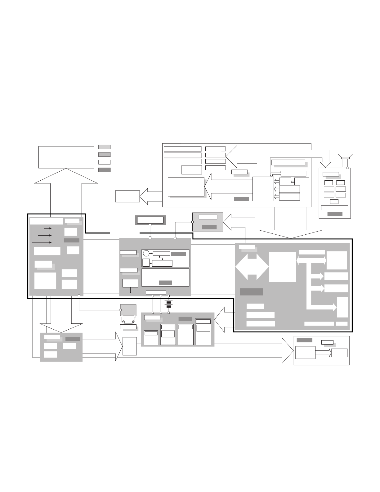
BLOCK DIAGRAM
Dimmer sensor
KIN4 EVCC3
DGND
4Pin FPC
2pin 2pin
3 Pin
10 Pin FPC
19 Pin FPC
30 Pin FPC
15 Pin FPC
74-pin rigid
10Pin FPC
24 Pin FPC
26 Pin FPC
8 Pin FPC
BUZZER
K–PCB
+
–
Down
MENU
DISP
SET
Back up
Capacitor
Voltage Detector
(Primary Battery)
Voltage Detector
(Secondary Battery)
Battery Detect SW
UP
7-contact
dial unit
Bcak light
Controller
LENS
UNIT
Xe
LAMP
1.8'' TFT
LCD Module
COD18T1029
VGH
VSS
VC1
VC2
VGL
GVDD
CP
GRES
CT1 SHUTTER
AFP0
AFPO
IRISD0 IRISD1
IRISD2 IRISD3
AFD0 AFD1
AFD2 AFD3
VCC5-1 MGND
GPCK
GSRT
STBYB1
RESET
VCOM
VBC
STBYB1
SRT
VSH
OE
CLR
MCLK
HCNT
SVDD
VG
VG
VR
HDB R G B FRP LCLK CLR
OE SRT HCNT GPCK GRES
GSRT CP LCDCTL BLCTL
LICS SDI SDO E2CS SCK
CT1 SHUTTER AFPI AFPO
IRISD0~IRISD3 AFD0~
AFD3 VCC5-1 VCC3-1 DGND
BLVCC VCC3 VCC1-1 VCC5
VCC515 VEE9 AGND MGND
XV1~XV4 DSUB CDSCS
ADCLK FR SHP SHD CLPDM
FH1 FH2 CLPOB OFDC
CD0~CD9 CH1~CH4 PBLK
PWCTLO PWCTL1 ADPTN CHG LTTRG
CENDN LEVELN F56 PWM OUT
VCC1-3 EVCC3 VCC3 VCC1.8 VCC5
VCC5-S DGND SGND AGND
BLCTL LCDCTL LCLK SRT CP GPCK
GSRT GRES OE HCNT CLR HDB
R G B FRP LIFCS E2CS SCK SDO
SDI AFD0~AFD3 CT1 SHUTTER
AFPO AFPI IRISD0~IRISD3
XV1~XV4 DSUB CDSCS ADCLK FR
SHP SHD CLPDM CH1~CH4 CLPOB
CD0~CD9 OFDC PBLK FH1 FH2
VBBENB EXCOS BLCTL
KEYINTB MACT FOUT SRDY
PSDATA PSCK SRSTB
RESETB LCDCTL PWCTLO
PWCTL1 RTCREG FRESETB
CFCOVER RED VCC1-3
VCC5 VCC3 EVCC3 DGND
VCC DGND
D+ D– RX
JKSW TX
VIDEO2
V4 V3A V3B V2 V1A
V1B VOUT VL CSUB
SUB VDD H1 H2 RG
DGND VCC5
SHTR+ SHTR– IRISM+ IRISM–
IRISS+ IRISS– AFA– AFA+
AFB– AFB+ AFCTHD AFPIDET
VCC33LZ VDD-AF
ST–BLOCK
VCC3
3.3V
BLVCC
BLGND
BLCNTB
BLVCC
8.0V
VCC4
1.8V
Photo
Sensor
VCC3-1
3.3V
VCC5
5.0V
GND
Power Supply Controller
SGND
Comparator
High voltage
generator
SGND
DGND
DGND
DGND
DGND
MGND
GND
VCC5-1
5.0V
EVCC3
3.3V
PW–BLOCK
D–BLOCK
CCD
H–BAFFER
V–Dr
HG75M
(SPEED)
Address DATA EX
SH7709A
Temperature Sensor
SDRAM x2
CF
CF SW
C–FPC
ICX252AQ
CCD
H–BAFFER
TC74VHC04AFT
x 2
H1 H2 RG
CF LED(GREEN)
128Mbit
FLASH/MASK Memory
16Mbit
Address
DATA
Address
CFDATA
Address
DATA
VIDEO Driver (75 Ω)
Serial
Transport
Buffer
USB Buffer
BLVCC
(BLGND)
BL–PCB
82-pin rigid
JK–PCB
DC
JACK
SERIAL
JACK
VIDEO
JACK
USB
JACK
Fuse X 4
Fuse X 3
Battery
Fuse X 3
Fuse X 3
Common
Choke
Common
Choke
Common Choke
GND
JK–IN
L–BLOCK
Power Supply Controller
CCD–BLOCK
AD9803
CDS/AGC/ADC
MD–PCB
Moter
DRIVER
Shutter
DRIVER
EEPROM
Moter
DRIVER
V-Dr
CXD3400N
RB5P0050M
RGB Tr ansport Interface
RGB
Filter
AGND
VCOM
Amp
VCC3-1
14.15V
VCC2
8.0V
VOD
3.0V
Flash LED (Orange)
ST UNIT
Flash Key
FLED FRLED FGLED PRLED PGLED
POFFB REC/PLAY SHUT1 SHUT2
EVCC3 ANO AN1 AN2
EVCC3 KIN0 KIN1 BUZ+ BUZ– DGND BTYP
S1 S2 S3 S4 S5 S6 S7 S8 S9 S10
S11 S12 S13 S14 S15 S16 S17
S18 S19 S20 COM1 COM2
OUT SGND SCR IGBTN
VCC5-S IGBT-OFF
SHUTTER
MACRO Key
TIMER key
SUB–FPC
HD404889
4 bit
Microprocessor
4 bit Microprocessor-BLOCK
Hardware reset
RTC–
4574JE
Power SW
REC/PLAY
SUB–LCD
Focus LED
(Two-color)
Power LED
(Two-color)
· · ·Normal PCB
· · ·Rigid flexible PCB
· · ·Reinforced FPC board
· · ·Direct lead wire
connected PCB
MAIN-PCB
Page 6
PCB
MAIN PW
D
L
BL
SUB
C
MD
Circuit Block
Main Power Supply
Lens Unit AF Power
CCD 5V Power Supply
Shutter Power Supply
Flash Control Power
Video Driver Power Supply
CCD Power Supply
BL Power Supply
Charging Booster Circuit
Charging Conparator
Stand-by Power
MPU
CPU
Flash Memory (Mask ROM)
SDRAM
BUS BUFFER
Video 75 ohm driver
Serial transport driver
V driver
CDS/AGC/ADC
TFT-LCM
RGB Interface
LCD Power Supply
LCD Power Supply (VDD)
VCOM-Amp
EEPROM
Inverter Circuit
4 bit Microprocessor
(Mask ROM)
RTC
Back up Capacitor
SUB-LCD
Switch/Key
CCD
H driver
AF/AE Motor driver
Shutter driver
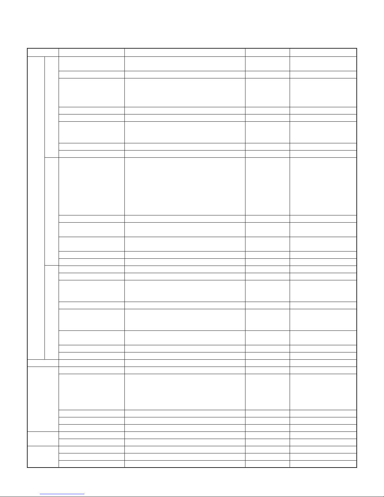
CIRCUIT BLOCK
Outline
1.8V Non adjustable step down transformer
3.3V Non adjustable step down transformer
3.3V Non adjustable step down transformer
5.0V V oltage regulator
Power specifications (+15V, -7.5V)
8.0V Up Converter
300V Booster
Current control circuit
Charging control circuit
Light emission control circuit
3.3V Regulator (EVCC)
Serial Interface
CCD Interface
VIDEO/RGB Encoder
JPEG
DMA Controller
BUS Interface
USB Interface
Built-in DRAM 2MB
32bit CPU (SH3)
16 Mbit (1 M x 16 bit) Flash Memory
64 Mbit (1 Mword x 16 bit x 4 bank) x 2
CF ADRESS BUS BUFFER (3 state buffer)
Vertical register driver
CDS
11 bit Programmable Gain Amplifier
10 bit A/D converter
1.8'' high definition TFT (556 x 220)
Serial data RGB interface
Writes picture quality, contrast, br ightness, gamma
data in serial
Power specifications (+5.0V, +14.75V)
fly-back transformer
3.3V Regulator
VCOM-AC/DC Adjustment
4 Kbit (256 word x 16 bit)
Inverter transformer shape is modified (Po wer Supply=8.0V)
LCD driver
Power ON sequence
Key scanning
Beep control
I/O and others
Built-in 32 KHz clock real time clock
Watch backup
3340,000 picture element interline
Horizontal register driving buffer x 2
1 - 2 phase excitation
Main Devices
S-8520B18
S-8520B33
S-8520B33
MAX685
S-8327B54MC
RN5RL33A
HG75M
SH7709A
LH28F160S3B
KM416S4030
and others
TC74AC367FT
TK15405MTL
CXD3400N
AD9803
C0D18T1029R
RB5P0050M
MB3800PFV
RN5RL33AA
NJM3414AV
BR93LC66FV
HD404889
RTC-4574JE
ICX252AQ
TC74VHC04AFT
LB1846M
C9201A
Note
No adjustments
No adjustments
No adjustments
Adjustment
No adjustments
Newly employed transformer
No adjustments
CSP264pin package
CSP208pin package
Compatible with the Mask Rom
CSP package
— 4 —
Page 7
■ Preparation
1. PC (IBM Compatible)/OS:Windows 95/98
2. Link cable.
3. Adjustment program
1) ADJ711.exe (Color adjustment data transfer program)
2) fload.exe (Camera unit version up program)
3) 711rom.bin (Camera unit program data)
4) 711gmenu.bin (Camera unit menu display data)
4. AC adaptor or stabilizer
5. Digital oscilloscope
6. Multimeter
7. Ammeter
8. Frequency counter
9. TV (with video terminal)
ADJUSTMENT
10. Video cable
11. Battery (battery operation/battery cover lock)
12. PC link program : Photo Loader (Communication function confirmation)
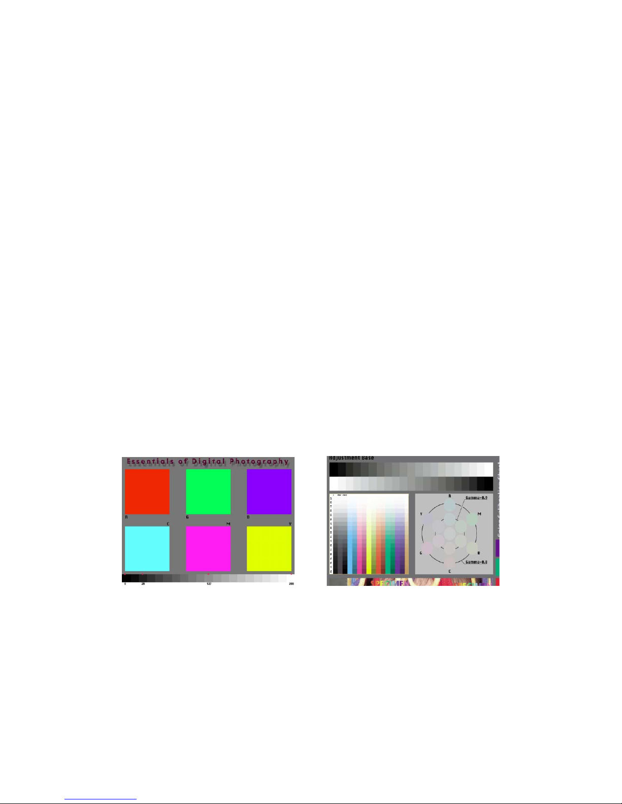
CHART2.JPGCHART1.JPG
■ Notes
Normally power is supplied using AC adaptor.
When error occurs, use a voltage regulator, and supply the specified power.
Make sure to confirm video output specifications (NTSC or PAL) after exchanging the MAIN-PCB.
— 5 —
Page 8

1. Program version upgrading
In the camera unit, program and graphic menu are stored.
Please check the version and update it if the version is not updated.
There are two method of program updating; using CompactFlash card or utilizing PC link cable.
Note:
1. Be sure to use AC adaptor.
2. If Mask ROM is mounted on the unit, updating the program is not possible.
1-1. How to confirm the program (graphic menu) version
1. Boot the test mode.
Turn the power on while pressing DISP and MENU buttons simultaneously.
2. Check the LCD display.
(Example)
TEST MODE
PROG 00. 07. 28. 20. 01 r Program version
GMENU 99. 12. 27. 18. 12 r Graphic menu version
· · · ·
1-2. Upgrading procedure using the CompactFlash card
(1) Copy the latest program ( 711rom.bin) and graphic menu ( 711gmenu.bin) on a CompactFlash card
then set the CompactFlash card on the camera.
(2) Connect an AC adaptor on the camera.
(3) Press DISP and MENU keys simultaneously and set the unit in PLAY mode then turn the power on.
Upgrading starts automatically.
Both program and graphic menu are upgraded.
(4) After about 40 seconds, upgrading is completed and unit turns the power off automatically.
(5) Chgange the CompactFlash card with the one for picture taking.
(6) Boot the test mode and confirm the program version.
Press DISP and MENU keys simultaneously and set the unit in PLAY mode then turn the power on.
(7) Finally, check the camera's function (shooting and playback).
— 6 —
Page 9
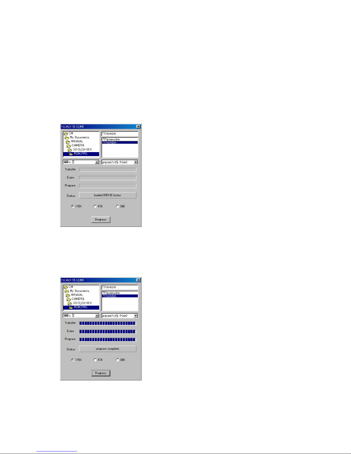
1-3. Upgrading procedure using the PC link cable
[Note]
Try the following methods when upgrading using CompactFlash card is failed and the unit cannot be turned
on. It may succeed the upgrading.
(1) Turn the camera off and extract CompactFlash card.
Close CompactFlash card cover and extract battery.
(2) Connect AC adaptor and PC link cable on the unit.
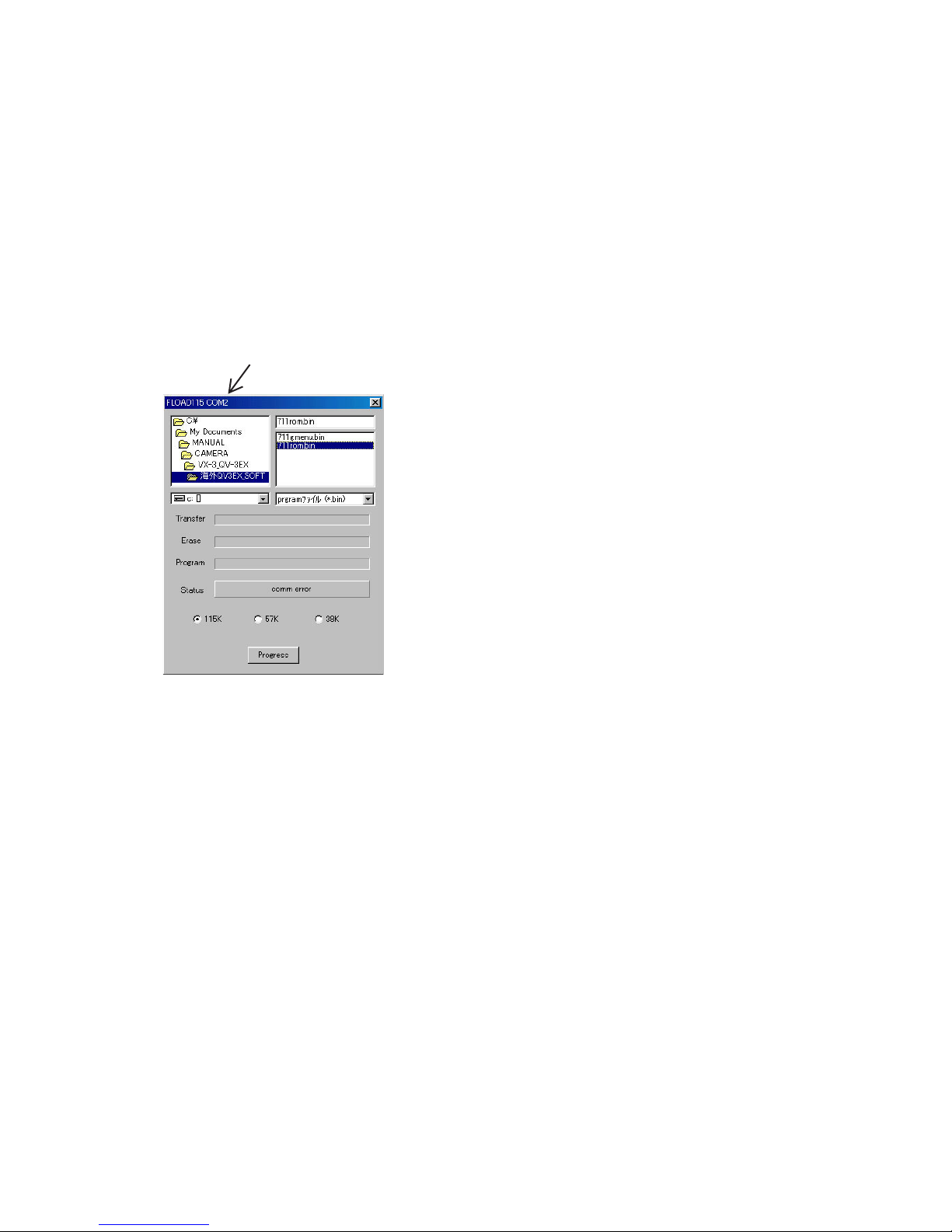
(3) Boot the transmission program (fload.exe).
(4) Choose program file ( 711rom.bin) or graphic menu file (711gmenu.bin).
(5) Select data transmission speed (115K/57K/38K).
(If errors occur, lower the transmission speed.)
(6) Click Progress button.
(7) Turn the camera on within 5 seconds.
(8) Data transmission starts.
(9) Data transmission is completed nor mally when Status box shows "program complete."
(10) Disconnect AC adaptor plug (cannot be turned off by the power switch).
(11) Change the CompactFlash card with one for shooting.
— 7 —
Page 10
(12) Boot the test mode and confir m the version.
Turn the camera on while pressing DISP and MENU buttons.
(13) Shoot a picture and confirm the camera function (shooting and playback.)
[Note]
In default, COM port 1 is set. If other port is used, boot it using MS-DOS prompt with fload port number
(1 – 4).
<Example>
fload 2 [Enter]; this sets COM port 2.
COM 2 is shown here
— 8 —
Page 11
2. Test mode
Note: Do not perform the menu item unless explained here.
(It may damage the internal data and camera becomes unusable.)
2-1. Booting
To boot the test mode;
Turn the camera on while pressing DISP and MENU buttons.
To boot MENU1
Press DISP ➜ DISP ➜ MENU keys in order rapidly.
To boot MENU2
Press FLASH ➜ FLASH ➜ MENU keys in order rapidly.
To boot MENU3
Press SELF ➜ SELF ➜ MENU keys in order rapidly.
* T o ex ecute
Use + or – keys to select a test item then press shutter button to execute it.
2-2. Item for testing
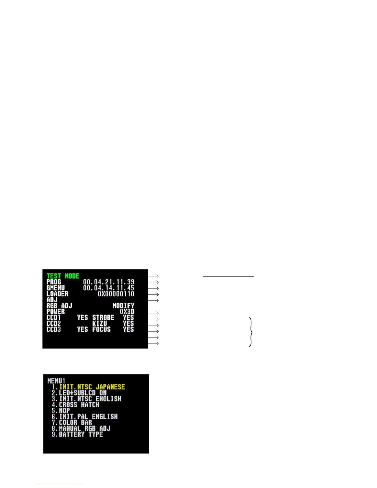
1 TEST MODE
2 MENU1
• TEST MODE
• PROGRAM Version
• Graphic Menu Version
• Loader Version
• ADJ
• Power MCU Version
• CCD ADJUST 1 (Yes/No/NG)
• CCD ADJUST 3 (Yes/No/NG)
• STROBE ADJUST (Yes/No/NG)
• KIZU ADJUST (Yes/No/NG)
• FOCUS ADJUST (Yes/No/NG)
Indicates in green-color if all items
have been adjusted.
Indicates "YES" if adjustments have
been completed.
Indicates "NO" if adjustments have
not been proceeded.
Indicates "NG" if an adjustments
failure occurred.
— 9 —
Page 12
3 MENU2
4 MENU3
— 10 —
Page 13
3. Adjustment
3-1. Color adjustment data writing
3-1-1. Note
(1) Set of lens ass’y adjusted in the factory and a floppy disc containing the lens’ adjustment data are
provided as a spare part.
(2) These adjustment data are stored in the EEPROM on MAIN-PCB.
(3) Help command on adjustment window cannot be used as it uses Japanese system.
3-1-2. The example which must be adjusted
It is necessary to write color adjustment data for the replacements of the following units.
(1) Lens ass'y : [3-1-3]
(2) MAIN-PCB (when EEPROM contents can be read) : [3-1-4]
(3) MAIN-PCB and lens ass'y (when EEPROM contents cannot be read) : [3-1-5]
3-1-3. To replace the lens ass'y
(1) Connect AC adaptor and PC link cable to the camera.
Note: Connect the link cable to serial port COM1.
(2) Turn the camera on to set it on PLAY mode.
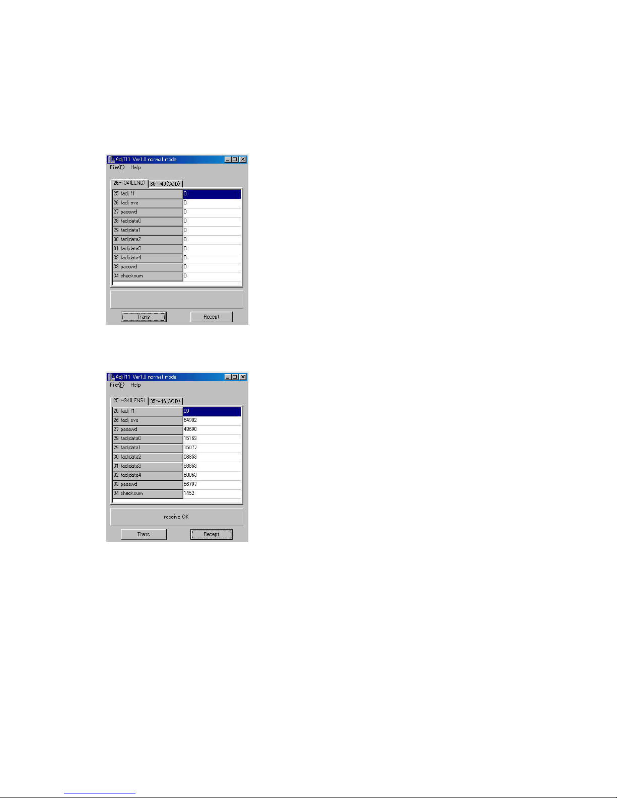
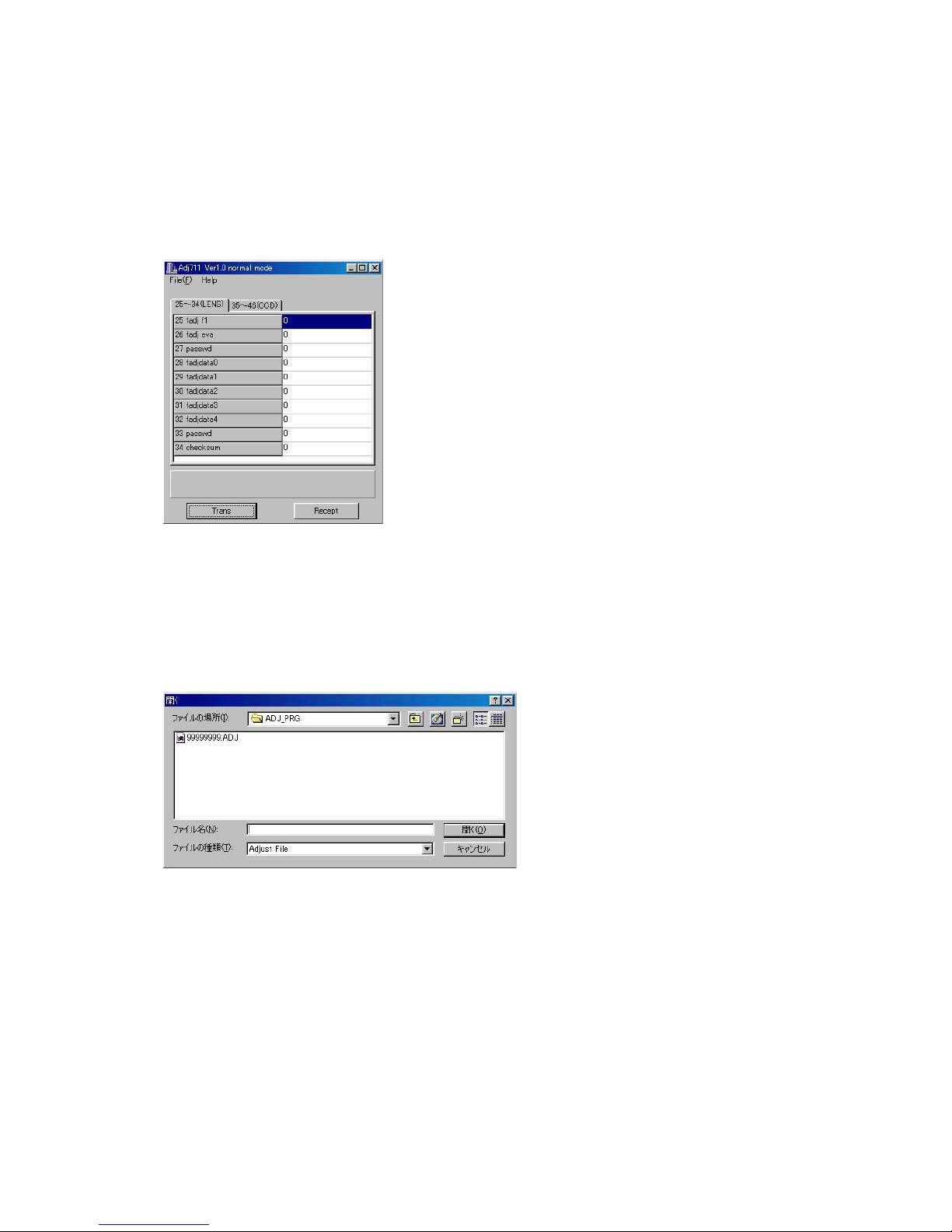
(3) Boot adjustment program adj711.exe.
At this time, each adjustment data are 0.
— 11 —
Page 14
(4) Read the adjustment data of before repairs.
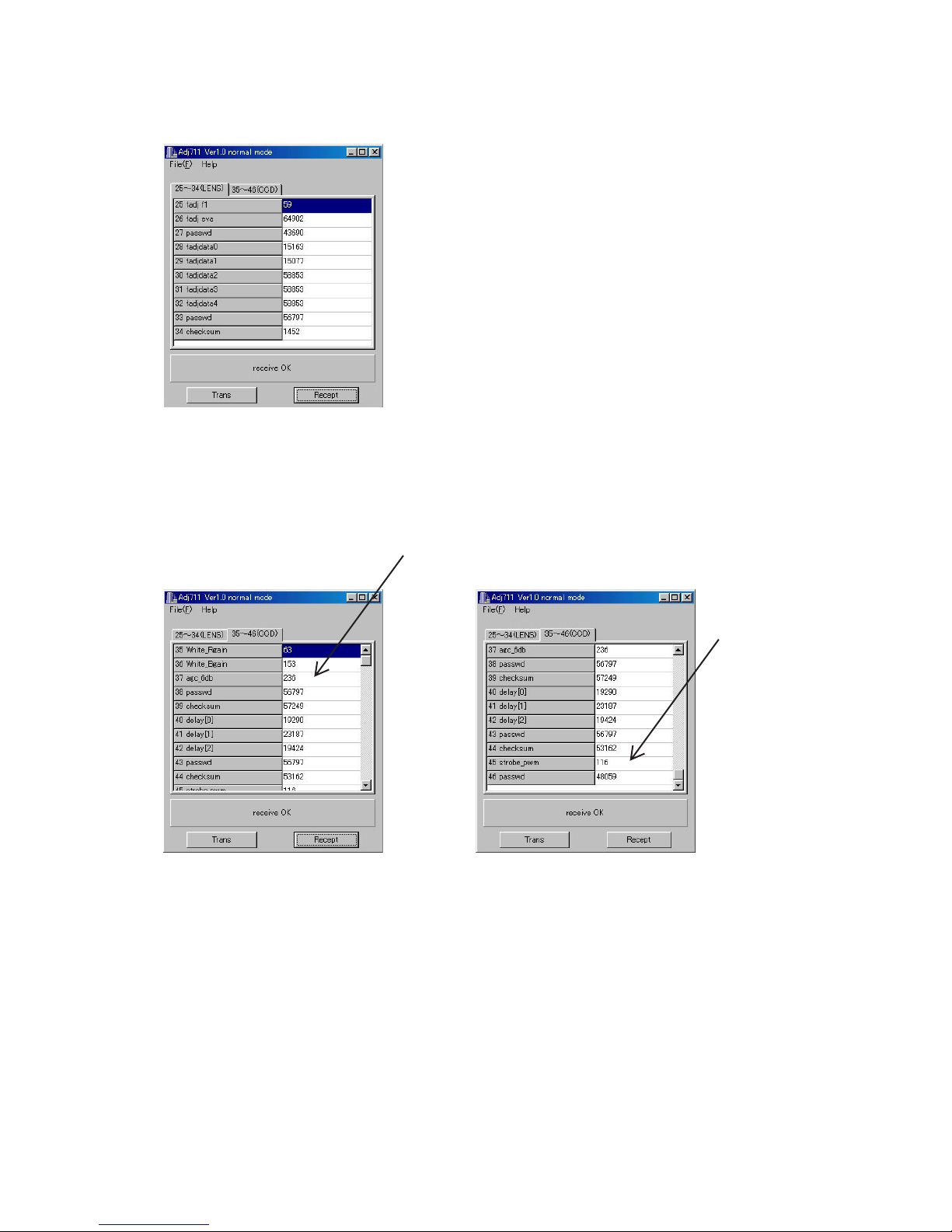
Click the Receipt button. “receive OK” will be indicated and adjustment data are shown.
Reference: At this time you can save the adjustment data in your PC.
File (F) ➜ Save as (A)
Select the drive and name the file then save it.
(Note: Do not forget to put extension code ".ADJ".)
(5) Write down the following numbers.
37 agc_6db
45 strobe_pwm
(6) Replace the lens ass'y.
(Adjusted in the factory and comes with adjustment data)
(7) Connect AC adaptor and PC link cable to the camera.
(8) Turn the camera on and set it on PLAY mode.
(9) Boot the adjustment program (adj711.exe).
— 12 —
Page 15
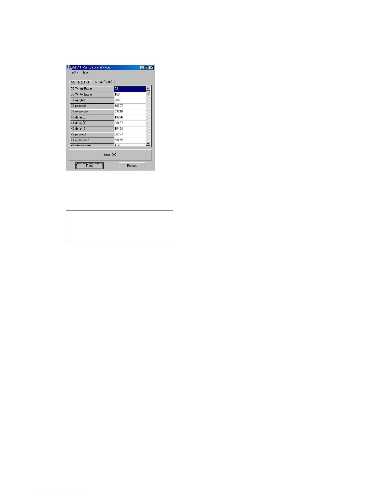
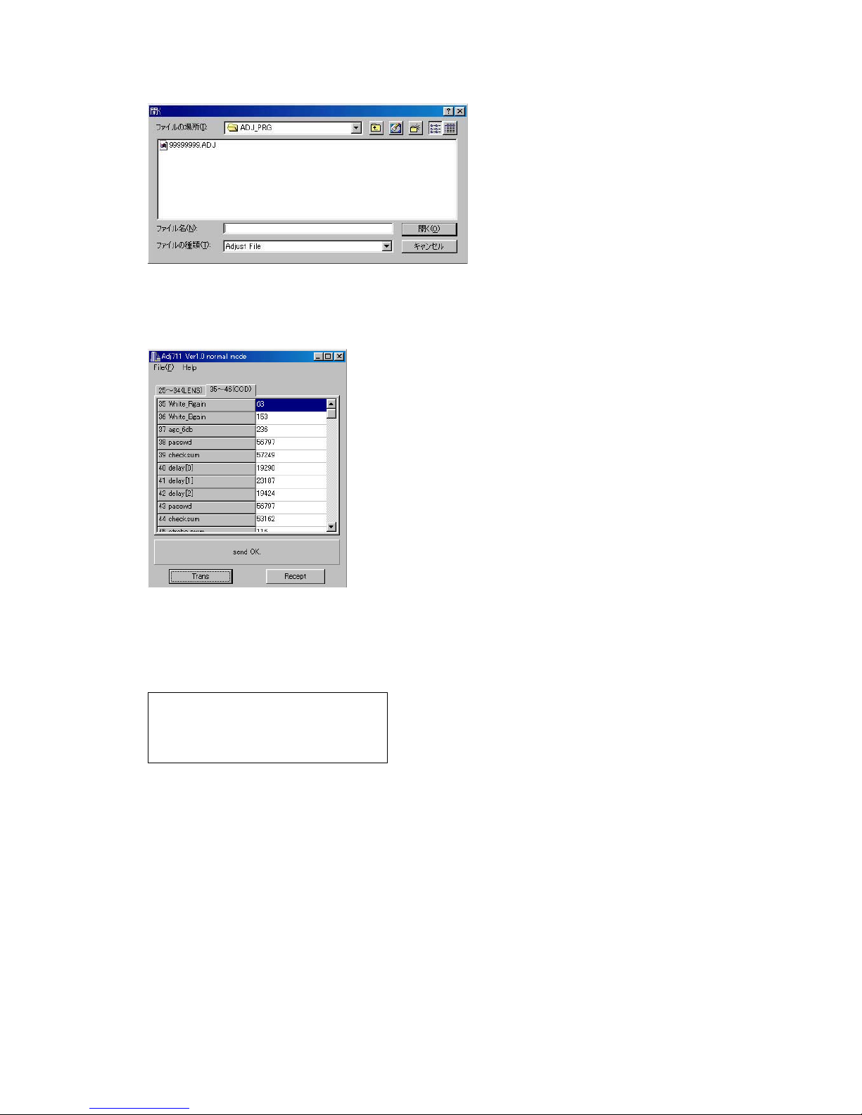
(10) Insert the floppy disc containing adjustment data of the lens ass'y in your PC and read the data.
File (F) ➜ Open (O)
Select FDD
Select adjustment data file with extension code .ADJ.
The file cannot be displayed if there is no extension code adj. In such a case, change the file name and
extension code “adj” using Explorer.
* Adjustment data file name: 99999999.ADJ
* 99999999 is the 8-digit number written on the seal stuck on the side of the lens unit.
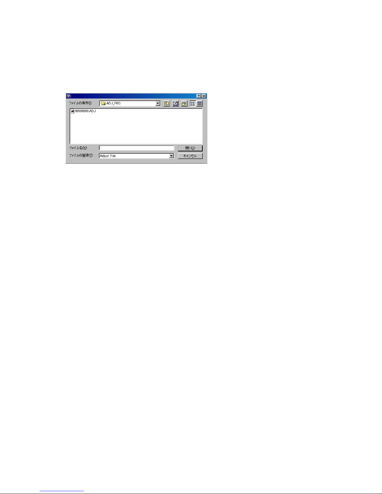
(11) Change the following data with the number you have written on step 5 (data before replacing the lens
unit).
Caution: Never change the other data.
37 agc_6db
45 strobe_pwm
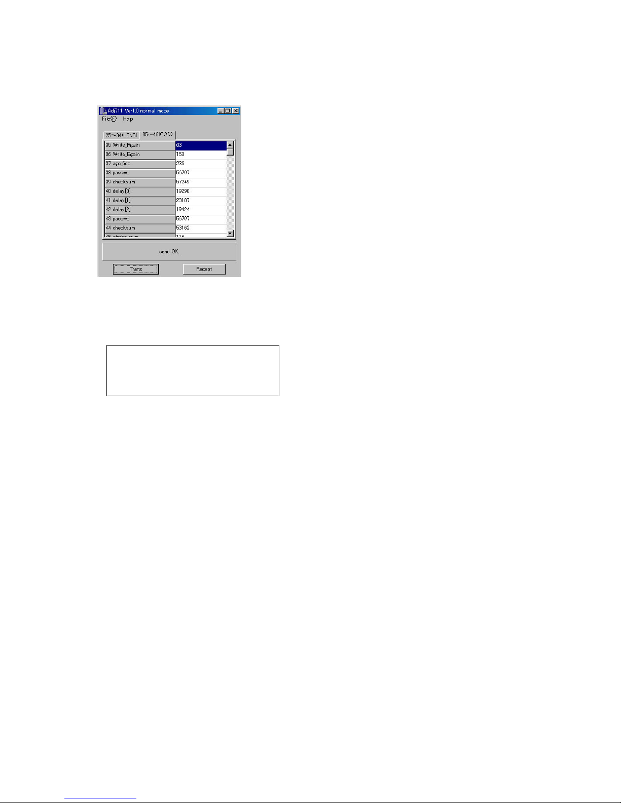
(12) Input the sum of four values in Checksum column.
(Example) 35 White_R gain 63
+
36 White_B gain 153
+
37 agc_6db 236 (Changed value)
+
38 Passwd 56797 (Fixed value)
||
39 checksum 57249 (Total value)
Note: If erroneous nuber is input, color adjustment cannot be done.
— 13 —
Page 16
(13) Transfer the data to the camera.
Click Trans button on ADJ window.
“send OK” will be shown.
(14) Turn the camera off.
(15) Booting the test mode, be sure that each adjustment item is YES.
Power on while pressing DISP and MENU keys simultaneously.
CCD1
CCD2
CCD3
YES
YES
STROBE
KIZU
FOCUS
YES
YES
YES
(16) Check the camera operation by shooting a picture and play it back.
— 14 —
Page 17
3-1-4. To replace MAIN-PCB (in case the contents of EEPROM can be read)
(1) Connect AC adaptor and PC link cable to the camera.
Note: Connect the link cable to serial port COM1.
(2) Turn the camera on to set it on PLAY mode.
(3) Boot adjustment program adj711.exe.
At this time, each adjustment data are 0.
(4) Read the adjustment data of before repairs.
Click the Receipt button. "receive OK" will be indicated and adjustment data are shown.
(5) Save the adjustment data in the PC.
File (F) ➜ Save as (A)
Select a drive to save data.
Name a file name then save the data.
(It is better to name the camera's serial number as the file name.)
XXXXXXXX.ADJ (Note: do not forget the extension code .ADJ.)
(6) Replace the MAIN-PCB.
(7) Connect AC adaptor and PC link cable to the camera.
(8) Turn the camera on and set it on PLAY mode.
(9) Boot the adjustment program (adj711.exe).
— 15 —
Page 18
(10) Load the saved data of the lens unit.
(11) Transfer the data to the camera.
Click Trans button on ADJ window.
“send OK” will be shown.
(12) Turn the camera off.
(13) Booting the test mode, be sure that each adjustment item is YES.
Power on while pressing DISP and MENU keys simultaneously.
CCD1
CCD2
CCD3
YES
YES
STROBE
KIZU
FOCUS
YES
YES
YES
(14) Check the camera operation by shooting a picture and play it back.
— 16 —
Page 19
3-1-5. In case of replacing MAIN-PCB and lens ass'y (EEPROM on MAIN-PCB contents cannot be read)
(1) Replace MAIN-PCB and lens ass'y.
(2) Connect AC adaptor and PC link cable to the camera.
Note: Connect the link cable to serial port COM1.
(3) Turn the camera on to set it on PLAY mode.
(4) Boot adjustment program adj711.exe.
At this point, adjustment data of each item is zero.
(5) Insert the floppy disc containing adjustment data of the lens ass'y in your PC and read the data.
File (F) ➜ Open (O)
Select FDD
Select adjustment data file with extension code .ADJ.and load it.
The file cannot be displayed if there is no extension code adj. In such a case, change the file name and
extension code “adj” using Explorer.
* Adjustment data file; 99999999.adj
* 99999999; 8-digit number printed on the seal on the side of camera
— 17 —
Page 20
(6) Transfer the adjustment data to the camera.
Clock Trans button on ADJ program window.
Send OK. Will be shown.
(7) Turn the camera off.
(8) Booting the test mode, be sure that each adjustment item is YES.
Power on while pressing DISP and MENU keys simultaneously.
CCD1
CCD2
CCD3
YES
YES
STROBE
KIZU
FOCUS
YES
YES
YES
(9) Perform the function check (Record/Playback).
(10) Perfor m the flash adjustment.
— 18 —
Page 21

3-2. Flash adjustment
1. General
When you exchange a flash unit, please perform this adjustment.
2. Necessary equipment
(1) Dar k room
(2) AC adaptor
(3) Gray paper (Superior's oxford gray No. 22)
The following sizes are available from us (also available from camra shop).
Parts code Parts name Specifications
1904 5411 Superior photographing background paper No. 22 (1.75 x 2.7m)
1904 5412 Sperior photographing background paper No. 22 (2.72 x 11m)
3. Condition
(1) Perform in a dark room.
(2) Distance between flash lens and gray paper should be 1 meter.
(3) Use lighter color of the gray paper.
Paper should be larger enough to fit in a picture taken from 1 meter distance.
(Reference; more than 1.5m x 2.0m)
4. Adjustment
(1) Connect an AC adaptor to the camera.
(2) Boot the MENU2 in the test mode.
Press DISP and MENU keys and turn the power on in REC mode.
Press FLASH ➜ FLASH ➜ MENU in order quickly.
(4) Using + and – keys, choose STROB ADJUST and press the shutter button.
(5) If the following display is indicated, turn the light off and press the shutter under the above conditions.
— 19 —
Page 22

(6) The flash flashes more than 10 times.
(7) Confirm the following indication and turn the camera off.
(8) Boot the test mode.
Turn the camera on while pressing DISP and MENU keys.
(9) Make sure that STROB ADJ column is YES.
(10) Turn the camera off.
5. Block diagram
Back ground paper.
1m
MF/
/
INFO
MENU
SET/
DISP
PLAY
OFF
REC
CARD
— 20 —
Page 23

3-3. Flash operation and recharge operation
1. General
When a flash is used and abnormal, check.
2. Conditions
•Set QV-3EX in “REC” mode.
•Normal Recording mode.
•Apply 6.0 ± 0.1 V voltage on DC in jack.
3. Preparation
(1) AC adaptor or stabilizer.
(2) Digital oscilloscope.
(2) Ammeter.
(3) TV (With video ter minal).
(4) Video cable.
4. Adjustment and checking
(1) Shoot a picture with flash OFF. (Make sure there is no flash)
(2) Shoot a picture with flash ON and make sure it flashes once.
(3) Shoot in red eye reduction mode and make sure it flashes twice.
(4) Connect QV-3000EX and TV with video cab le and mak e sure that the pictures taken in steps (2) and (3)
are not whitish, dark or erroneously colored.
(5) Make sure that the charging current is less than 1.3 A.
(6) Confirm the waveform at flashing with a digital oscilloscope and compare it with the waveform shown
on the next page.
5. Notes
(1) Excuete in a dark room.
(2) Shoot a colorful object as much as possible.
Digital oscilloscope
Bring the probe closer
to the camera
Flash lens surface
DIGITAL
VIDEO
OUT
USB
DC IN 6V
Video input cable
TIME : 1.0 µsec/DIV
VOLTS : 1 V/DIV(AC mode)
QV-3EX
TV monitor
(with a video input terminal)
— 21 —
Page 24

Flash trigger waveform
1. Normal waveform TIME : 1 µ sec/DIV
VOLTS : 1 V/DIV
CH1
The first pulse on
the positive side.
ACQUIRE
NORMAL
1V
ENVELOPE
757µV
It is OK if a wave-shaped waveform is generated up
to the second pulse on the positive side.
The first pulse on the negative side.
1
2
AVS
REPET
ON | OFF
SAVE ON
ON | OFF
UERT1µV
2. NG waveforms when trigger skipping occurs.
(1) When tr igger skipping occurs on the first
positive pulse.
(2) When trigger skipping occurs on the first
negative pulse.
— 22 —
Page 25

3-4. Current consumption
1. General
When consumption of a battery is early, check.
2. Conditions
•Set QV-3000EX to “PLAY” mode.
3. Preparation
(1) Voltage regulator.
(2) Ammeter.
4. Adjustment procedure
(1) Current consumption (DC in = 6.0 ± 0.1 [V])
• Make sure that current consumption is less than 550 mA in PLAY mode.
• Make sure that current consumption is less than 800 mA in REC mode.
(Flash charge current is not included)
(2) Lower the voltage from 6 V as shown below then make sure the battery war ning indicator changes.
DC in = 5.15 ± 0.05 [V]
— 23 —
Page 26

3-5. VCOM DC adjustment
1. General
Perform these adjustments when you replace LCD module or MAIN-PCB.
2. Preparation
(1) AC adaptor or stabilizer.
(2) Photo sensor/ Photo sensor amp (C2719)/L.P.F
(3) Digital oscilloscope.
3. Adjustment and checking
(1) Turn the power on while pressing DISP and MENU keys simultaneously. (TEST MODE)
(2) Push DISP ➜ DISP ➜ MENU keys in order rapidly. (TEST MODE 1)
(3) Select and execute VCOM-DC of MANUAL RGB ADJ.
(4) Monitoring the photosensor output with an oscilloscope via a 60 Hz cutoff L.P.F., adjust + or – keys so
that 60 Hz ripple component is minimum.
Photo diode
S1153
MF/
/
INFO
MENU
PLAY
OFF
REC
SET/
DISP
LCD
QV-3EX
L.P.F
Photo Sensor Amp
C2719
Oscilloscope
CARD
Minimize the
ripple components
— 24 —
Page 27

3-6. Operation check
1. Preparation
(1) Batteries.
(2) AC adaptor.
(3) PC (IBM compatible)/OS:Windows 95/98.
(4) Link cable.
(5) Photo loader (program).
(6) TV (with video teminal).
(7) Video cable.
(8) USB cable/USB driver
(9) Test chart (for photography check)
(That which carried out color printing of picture data "CHART1.JPG" and the "CHART2.JPG".)
2. Check matter
(1) Photography check (Please be sure to carry out.)
1 Shoot the test chart without flashing.
2 Shoot the test chart with flashing.
3 Confirm the result (compare with properly functioning camera) for;
• Color
• Focus and resolution
(2) Unti-shock check, Battery operations
(3) Power jack, switch, buttons operations
(4) CompactFlash insersion/eject operation, Cov er open/close operation, battery cover open/close operation.
(5) Resolution and color reproduction.
(6) Image reversing, Normal/Macro switching, AE operation , AF operation, Self-timer count down displa y,
exposure adjustment function, flash display function, self-timer function.
(7) Video output, digital communication, USB function.
(8) Flash operation.
(9) Dust and scratches on lens.
(10) Exter nal inspection.
3. Note
(1) Make sure Video out setting are appropriate to your country.
(i.e. Japan=NTSC, England = PAL)
4. Test chart picture
CHART2.JPGCHART1.JPG
— 25 —
Page 28

DISASSEMBLY
1. Tool
Soldering iron / solder / desoldering wire
Precision screwdrivers / Tweezers
Discharge tool (Resistor 1.5 kΩ 5 W) / Pliers
2. Remove battery and CF card.
4. Remove the screws at the other side (× 2).
Screw
5. Remove the screws at the bottom (× 4).
3. Remove two screws at the side of the camera .
Screw
Screw
6. While pushing the botton, open the case.
7. Remove the upper case from the bottom as
shown on the figure.
— 26 —
Page 29

8. The figure shows the camera whose upper case
has removed.
12. The figure shows the side cover opened.
9. Open the CF cover.
10. Insert the screwdriver (–) between the cases.
13. Remove the bottom case.
14. Rotate the upper case pivotting on the rotary
switch.
11. Open the case with twisting the screwdriver.
15. Slowly remove the upper case not to damage
the shutter bottom and the switch.
— 27 —
Page 30

16. The figure shows the back side of the camera
case opened.
20. Insert the screwdriver (–).
17. The figure shows the front side of the camera
case opened.
18. Peel off the waring label.
21. Pry up the indicator block with screwdriver.
22. Insert the screwdriver (–).
19. Discharge flash capacitor by discharging tool.
23. Remove the indicator block with screwdriver.
TerminalTerminal
— 28 —
Page 31

24. Remove the cable.
Cable
28. Remove a screw (black) on MD-PCB.
25. Remove the cable.
Cable
26. Remove a screw (black).
29. Remove the cable.
30. Insert a screwdriver (–) bewtween space shown
in the figure.
Screw
27. Remove the connector.
31. Pry up MD-PCB with a screwdr iver.
— 29 —
Page 32

32. Remove the cable.
36. Remove a screw (Zinc × 1).
33. Remove the cables (white × 1, black × 1) by
desoldering.
34. Remove the switch cable.
37. Remove a screw (black × 1).
38. Remove the switch.
35. Remove the screws (Zinc × 4).
Screw
39. Remove the screw on the side (black × 1).
— 30 —
Page 33

40. Remove a screw (Ni 8mm × 1).
Screw
44. Remove the MAIN-PCB ass’y.
41. Insert a screwdriver (–).
42. Unhook the MAIN-PCB ass’y.
45. Remove the JK-PCB screws (Ni × 2).
Screw
46. Remove the screws on flash block (black × 2).
43. Pull up the MAIN-PCB ass'y from the bottom.
Screw
47. Desolder two of battery springs on JK-PCB
(× 2).
— 31 —
Page 34

48. Remove JK-PCB.
52. Insert a screwdriver (–).
49. Remove flash block.
50. Figure shown MAIN-PCB ass’y removed from
chassis
53. Unhook the ass’y by pr ying down the screwdriver.
54. Open the D-PCB.
51. Remove screw (Ni × 1)
55. Figure shown D-PCB opened.
— 32 —
Page 35

56. Remove a screw on L-PCB (Zinc × 1).
Screw
60. Figure shows MAIN-PCB ass’y removed from
chassis.
57. Remove a screw on L-PCB (BLACK × 1).
Screw
58. Remove two screws on PW-PCB (Zinc × 2).
61. Remove the connector.
62. Remove DISP button.
Screw Screw
59. Remove MAIN-PCB ass’y from chassis.
63. Peel off KEY-PCB at one side by using a
screwdriver.
— 33 —
Page 36

64. Peel off KEY-PCB at the other side b y using the
screwdriver .
68. Peel off SUB-PCB with using a screwdriver (–).
65. Figure shows removed KEY-PCB.
66. Remove metal fittings on SUB-PUB (two places
are calked).
69. Peel off SUB-PCB.
70. Peel off SUB-PCB.
67. Remove SUB-LCD.
71. Remove SUB-PCB from the chassis.
— 34 —
Page 37

72. Remove screws on the optical lens (Ni × 2).
Screw
73. Remove the lens.
76. Remove the battery cover.
74. Remove the screws (Ni × 1).
Screw
75. Remove the frame.
— 35 —
Page 38

Notice in assembly procedure
1. Make sure that all parts are back in shape if
those has been deformed when assemble.
2. Building MAIN-PCB into chassis.
(1) Place MAIN-PCB as shown below.
(4) Put L-PCB through chassis.
(5) Put PW-PCB into the square hole on the
chassis.
(2) Put JK-PCB through the ring shaped
cable of flash block.
(3) Replace JK-PCB where it was.
(6) Put PW-PCB into the gash on the
chassis.
(7) Assemble the flash capacitor block.
— 36 —
Page 39

(8) Fix L-PCB into the square hole on the
chassis.
(12)Reassmble D-PCB.
(9) Fix L-PCB by driving a screw (Zinc × 1).
(10)Fix L-PCB by driving a screw
(black × 1).
(13)Put D-PCB into the gash on the chassis.
(14)Assemble D-PCB with pushing the par t
as shown in the figure.
(11)Fix PW-PCB by driving two screws
(Zinc × 2).
Screw
(15)Drive a screw as shown (Ni × 1).
— 37 —
Page 40

3. Building MAIN-PCB into the frame (summary).
(1) Build MAIN-PCB into the frame.
(2) When they are assembled.
(5) Assemble JK-PCB cable.
(3) Fix the gray cable of flash block onto the
MAIN PCB.
(4) Fix three cables of flash block onto the
MAIN PCB.
— 38 —
Page 41

4. Build the frame into the case.
Pin on the shutter button or the shutter switch
may be damaged when building the frame
into the case without knowing the below
notice.
(1) Open the CF cover and put the trame into
the case from rotary switch part.
Be careful not to close it completely.
(4) Build the frame into the case , then
remove the plate.
(2) Prepare a plate made of thin resin.
(3) Insert the plate between chassis button
and chassis switch.
— 39 —
Page 42

EXPLODED VIEW
4-1
38
21-2
41
40
N1
S1
× 2
43
42
× 2
39
23
51
4-3
4-2
4-3
3
S8
× 3
4
5
1
2
45
S1
S7
54
48
52
34
47
53
S1
46
49
S7
× 3
10-1
44
23
50
10-2
3637
33
35
32
6
7
8
9
10
S6
21-3
31
10-3
30
S1
× 2
22
21-1
21
S7
S7
22
× 2
S8
24
S3
18
× 2
19
25
26
S1
S1
× 3
S4
S7
23
29
28
27
S1
16
17
10-4
11
12
13
× 2
14
15
20
S8
— 40 —
S8
× 2
Page 43

QV-3EX
MAIN BODY COMPONENT
N Item Code No. Parts Name Specification Q Price Code R
N 1 1001 9229 CASE/CENTER K241310-1 1 AB X
N 2 1001 9233 TAPE/DOUBLE SIDE K441932-7 1 AA X
N 3 1001 9234 TAPE/DOUBLE SIDE K441988-1 1 AA X
N 4 1002 2620 ASSY/FRONT PANEL K342194*1 TK(K711) 1 CO X
N 4-1 1001 9230 BUTTON/MODE K341781-1 1 AG X
N 4-2 1001 9231 PANEL/DISPLAY B-K711 K441928-1 1 AB X
N 4-3 1001 9232 TAPE/DOUBLE SIDE K441932-1 2 AA X
N 5 1001 9222 KNOB/PW K341783-1 1 AA X
N 6 1001 9223 FRAME/PW K341784-1 1 AA X
N 7 1001 9224 BUTTON/PW K341785-1 1 AA X
N 8 1002 2090 SPRING/PW K442301-1 1 AA X
N 9 1001 9221 PLATE/PW K341782-1 1 AA X
N 10 1002 2625 ASSY/DISPLAY K342198*1 TK(K711) 1 CI A
N 10-1 1001 9249 PANEL/DISPLAY A-K711 K341825-1 1 AJ X
N 10-2 1001 2616 LCD COD18T1035FN 1 DE A
N 10-3 1002 2624 ASSY/BL K342197*1 TK(K711) 1 BZ A
10-4 3851 2113 FLUORESCENT LAMP CAS-1.8JS1.8-1 1 AW A
N 11 1002 6388 UNIT/LENS K342200*1 TK(K711) 1 EJ A
N 12 1001 9170 TAPE/DOUBLE SIDE K442069-1 1 AA X
N 13 1001 9168 PLATE/LENS K441981-1 1 AH X
N 14 10019216 BUTTON/SHUTTER K341823-1 1 AG X
N 15 1002 2626 ASSY/CF COVER K241437*1 TK(K711) 1 AY A
N 16 10019169 TAPE/DOUBLE SIDE K442003-3 1 AA X
N 17 1001 9162 COVER/FINDER K341779-1 1 AF X
N 18 1002 2629 ASSY/REAR PANEL K241438*2 TK(K711) 1 CO X
N 19 1002 0902 PLATE/RATING K441965-2 1 AA X
N 20 1001 9163 PANEL/LENS K341820-1 1 AU X
N 21 1002 2631 PCB ASSY/MAIN K241440*1 TK(K711) 1 EJ A
N 21-1 1002 2606 PCB ASSY/STC K442260*1 TK(K711) 1 DN A
N 21-2 1002 2608 PCB ASSY/JACK K442261*1 TK(K711) 1 DN A
N 21-3 1001 4397 STROBE UNIT CO-711 1 CA A
N 22 1001 9152 CUSHION K442250-1 1 AA X
N 23 1001 9197 TAPE/DOUBLE SIDE K441932-5 6 AA X
N 24 1001 9213 CASE/CENTER K341827-1 1 AB X
N 25 1001 9211 TAPE/DOUBLE SIDE K441932-2 1 AA X
N 26 1001 9142 SHASSIS K241306-1 1 AL X
27 6613 1330 PIN/STRAP R340181-2 1 AE C
N 28 1001 9212 CASE/CENTER K341824-1 1 AB X
N 29 1001 9141 SWITCH UNIT IB-VC-Y0458 1 BY A
N 30 1001 9192 FRAME K140672-1 1 AD X
N 31 1001 9195 SPRING/BATTERY B-K711 K241313-1 1 AD X
32 1000 5396 PLATE/INSULATION K441867-2 1 AA X
N 33 1001 9194 SPRING/BATTERY A-K711 K241312-1 1 AC X
N 34 1001 9193 FRAME K140673-1 1 AH X
N 35 1001 9190 CUSHION K442004-1 1 AA X
N 36 1001 9196 SCREW/STAND K341787-1 1 AC X
N 37 1001 9201 SEAL/BLIND K442035-1 1 AA X
N 38 1002 2610 ASSY/BATTERY COVER K442280*1 TK(K711) 1 AX A
Notes: NEW : New registration parts
Q : Quantity used per unit
R : Rank
- 41 -
Page 44
N Item Code No. Parts Name Specification Q Price Code R
N 39 1001 9198 TAPE/DOUBLE SIDE K441932-8 1 AA X
N 40 1001 9214 CASE/CENTER K341828-1 1 AB X
N 41 1001 9164 COVER/JACK K341853-1 1 AB X
N 42 1001 9156 BUTTON/LCD K341780-1 1 AG X
N 43 1002 2623 ASSY/BUTTON K342196*1 TK(K711) 1 CH X
N 44 1001 9149 BUZZER 7BB-15-6A64 1 AJ X
N 45 1001 9199 PROTECTOR/FINDER K441961-1 1 AB X
N 46 1001 9157 CASE/SHIELD K341786-1 1 AA X
47 2725 1391 LCD CA487-TS 1 AL A
N 48 1001 2612 CONNECTOR K442024-1 1 AA X
N 49 1002 2609 PCB ASSY/SUB K442262*1 TK(K711) 1 CV A
N 50 1002 2637 PCB ASSY/MAIN K140754*2 TK(K711) 1 DP A
N 51 1001 9151 LABEL/CAUTION K442249-1 1 AA X
N 52 1001 9150 TAPE/DOUBLE SIDE K441932-10 1 AA X
N 53 1001 9270 CUSHION K442250-2 1 AA X
N 54 1001 9200 TAPE/DOUBLE SIDE K442003-1 1 AA X
N1 6392 2390 NUT A411287-1 2 AA X
N S1 1001 2551 SCREW BT3 1.7X3.5 BK 12 AA X
S2 5860 0420 SCREW BT3 1.7X4 NI 3 AA X
S3 5860 3458 SCREW BT3 1.7X8 NI 1 AA X
N S4 1001 9145 SCREW ST1 2.0X3.5 NI 1 AA X
N S5 1001 9146 SCREW ST3 1.7X3.5 BK 1 AA X
N S6 1001 9147 SCREW ST3 1.7X4.0 NI 0 AA X
N S7 1001 9154 SCREW ST3 1.7X4.0 ZMC 8 AA X
N S8 1001 9171 SCREW K442173-1 8 AA X
ACCESSORY
N Item Code No. Parts Name Specification Q Price Code R
N 1002 1142 AC ADAPTER/ CHARGER BC-7LA-WW 1 CY C
N 1000 6300 CABLE/POWER CBL-K799-AC-EU 1 AR C
N 1002 1138 CD-ROM(MS) CK711DEA01R 1 AL X
1015 1524 CARD/CF HB289008C4XA 1 DF X
N 1000 6298 CABLE/DC CBL-K799-DC 1 BC C
3502 2744 CABLE/USB 59204-2301 1 BK C
N 1002 1136 STRAP ST-K711 1 BB C
N 1002 1137 CASE/SOFT SC-711 1 BV C
1015 1471 CABLE/PC-LINK LC9F-DOS-K740-L 1 BU C
1014 8773 CABLE/VIDEO VC-K723-FC 1 AR C
N 1002 1141 BATTERY/LITHIUM-ION BATT-K796-LI-E 1 CV X
Notes: NEW : New registration parts
Q : Quantity used per unit
R : Rank
- 42 -
Page 45

PCB
N Item Code No. Parts Name Specification Q Price Code R
MAIN PCB
D811 2370 1393 LED SLR-332VC3F 1 AA X
FU102 2797 5616 FUSE PI-R43101.5 1 AC A
FU103 2797 5737 FUSE PI-R431.750 1 AC A
FU104 2797 5716 FUSE PI-R431002 1 AC A
FU105 2797 5737 FUSE PI-R431.750 1 AC A
N SW800 1001 5276 SWITCH SPVC21-T 1 AC C
SUB PCB
N C804 7740 3521 CONDENSER/BACKUP PAS621L-VL3 1 AT X
SW800 3412 1995 SWITCH/TACT SKQRAA-T 1 AB C
SW801 3412 1995 SWITCH/TACT SKQRAA-T 1 AB C
SW802 3412 1995 SWITCH/TACT SKQRAA-T 1 AB C
N SW810 1001 9105 SWITCH/SLIDE SSSS213-12-B 1 AD C
N SW830 1001 4578 SWITCH TSW-3D-T50 1 AC C
JK PCB
N JK190 1001 5273 JACK HEC3604-010120 1 AD B
JK194 3501 8197 JACK/MINI HSJ1169-019010 1 AF B
JK196 3025 1937 JACK HSJ1636-011020 1 AE B
KEY PCB
SW862 3412 1995 SWITCH/TACT SKQRAA-T 1 AB C
SW863 3412 1995 SWITCH/TACT SKQRAA-T 1 AB C
SW868 3412 1995 SWITCH/TACT SKQRAA-T 1 AB C
SW869 3412 1995 SWITCH/TACT SKQRAA-T 1 AB C
SW870 3412 1995 SWITCH/TACT SKQRAA-T 1 AB C
SW871 3412 1995 SWITCH/TACT SKQRAA-T 1 AB C
SW872 3412 1995 SWITCH/TACT SKQRAA-T 1 AB C
Notes: NEW : New registration parts
Q : Quantity used per unit
R : Rank
- 43 -
Page 46

PRINTED CIRCUIT BOARDS
MAIN PCB
MAIN-PCB consists of thres PCB.
Details are in the following page.
LINER-PCB POWER-PCB DIGITAL-PCB
DIGITAL-PCB POWER-PCB LINER-PCB
— 44 —
Page 47

DIGITAL-PCB (PCB 711-D)
— 45 —
Page 48

LINER-PCB (PCB 711-L)
— 46 —
Page 49

POWER-PCB (PCB 711-PW)
— 47 —
Page 50

SUB-PCB (PCB 711-SUB)
— 48 —
Page 51

BACK LIGHT -PCB (PCB 711-BL)
JACK-PCB (PCB 711-JK)
— 49 —
Page 52

KEY-PCB (PCB 711-K)
MD-PCB (PCB 711-MD)
— 50 —
Page 53

CCD-PCB (PCB 711-CCD)
FLASH-PCB (PCB 711-STC)
— 51 —
Page 54

— 52 —
SCHEMATIC DIAGRAMS
DIGITAL-PCB (PCB-K711-D)
Page 55

— 53 —
LINER-PCB (PCB-K711-L)
Page 56

— 54 —
POWER-PCB (PCB-K716-PW)
Page 57

— 55 —
SUB-PCB (PCB-K711-SUB)
Page 58

— 56 —
BACK LIGHT-PCB (PCB-K711-BL)
Page 59

— 57 —
JACK-PCB (PCB-K711-JK)
Page 60

— 58 —
KEY-PCB (PCB-K711-K)
Page 61

— 59 —
MD-PCB (PCB-K711-MD)
Page 62

— 60 —
CCD-PCB (PCB-K711-C)
Page 63

FLASH-PCB (PCB-K711-STC)
— 61 —
Page 64

CASIO TECHNO CO.,LTD.
Overseas Service Division
Nishi-Shinjuku Kimuraya Bldg. 1F
5-25, Nishi-Shinjuku 7-Chome
Shinjuku-ku, Tokyo 160-0023, Japan
 Loading...