

Page 1
SERVICE MANUAL
INDEX
(without price)
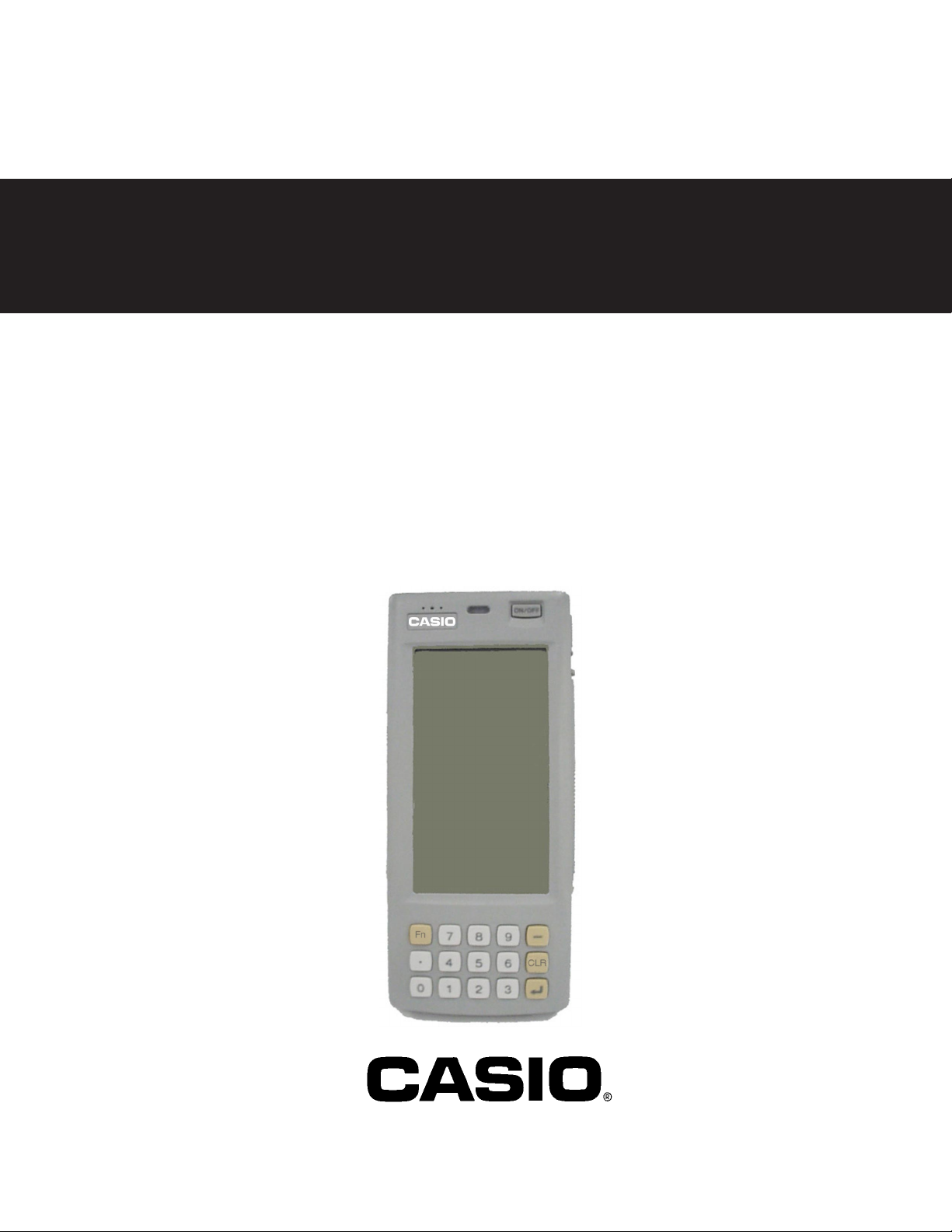
HANDY TERMINAL
IT-2000 (PX-704)
JAN 1998
Page 2

CONTENTS
1. SPECIFICATIONS ................................................................................................1
1.1 CPU .............................................................................................................1
1.2 Hardware.....................................................................................................1
1.3 Memory .......................................................................................................1
1.4 Touch Panel ................................................................................................1
1.5 Display ........................................................................................................1
1.6 Sound..........................................................................................................1
1.7 Key .............................................................................................................. 1
1.8 Interface ...................................................................................................... 1
1.9 PC card ....................................................................................................... 2
1.10 Power supply..............................................................................................2
1.11 Durability .................................................................................................... 2
2. OPTIONS .............................................................................................................. 3
3. INTERFACE PIN ASSIGNMENT .......................................................................... 5
3.1 8 Pin serial I/F ............................................................................................. 5
3.2 14 Pin serial I/F (RS-232C)......................................................................... 5
3.3 Card I/F........................................................................................................ 6
4. SYSTEM DIAGRAM .............................................................................................8
4.1 System diagram ......................................................................................... 8
4.2 Block diagram ............................................................................................ 9
4.3 PCB diagram ............................................................................................ 10
4.4 Power supply diagram ............................................................................. 11
5. CIRCUIT DESCRIPTION ....................................................................................12
5.1 Memory .....................................................................................................12
5.2 KBC ........................................................................................................... 15
5.3 Communication ........................................................................................ 21
5.4 PC Card .....................................................................................................22
5.5 Power Supply ...........................................................................................24
6. DISASSEMBLY .................................................................................................. 26
6.1 Removal of the main battery and the backup batteries ....................... 26
6.2 Removal of the battery pack cover ........................................................ 26
6.3 Removal of the Lower case block .......................................................... 26
6.4 Removal of SUB ass’y PCB ....................................................................27
6.5 Disassembly of the Middle Case Block ................................................. 27
6.6 Disassembly of Upper Case Block ......................................................... 29
7. DIAGNOSTIC PROGRAM.................................................................................. 30
7.1 General...................................................................................................... 30
7.2 Inspection Detail ...................................................................................... 32
7.3 Special tool ...............................................................................................33
7.4 Diagnostic test ......................................................................................... 35
8. CIRCUIT DIAGRAMS ......................................................................................... 53
8.1 Curcuit diagram INDEX ........................................................................... 53
9. EXPLODED VIEW .............................................................................................. 75
10. PARTS LIST........................................................................................................76
Page 3

1. SPECIFICATIONS
1.1 CPU CPU: Intel 80486 GX (32 bit)
Clock: 25M Hz
1.2 Hardware Configuration: IBM PC AT Architecture and dedicated hardware
1.3 Memory Main memory:
4MB 16Mbit DRAM × 2
File memory:
0MB (for D10 Model)
4MB 32Mbit NAND Flash × 1 (for D20 Model)
8MB 32Mbit NAND Flash × 2 (for W30, D30P Model)
DOS & BIOS Memory:
1MB 8Mbit Flash E2PROM × 1
MASK ROM:
8MB 64Mbit MASK ROM × 1 (W30 Model only)
Video Memory:
512KB 4Mbit DRAM × 1
HW Window Memory:
32KB 256Kbit SRAM × 1
1.4 Touch Panel Type: Analog Type
Resolution: 192 × 384 dots
1.5 Display LCD Type: FSTN semi-transparent LCD
Resolution: 192 × 384 dots
Back light: EL back light (with auto-off function)
Character type: Alpha-numeric (ANK), user defined characters
Character size:
Normal size 12 dots: 6 × 12 dots
(Alpha-numeric) 16 dots: 8 × 16 dots
24 dots: 12 × 24 dots
Double size 12 dots: 12 × 12 dots
(Kanji) 16 dots: 16 × 16 dots
24 dots: 24 × 24 dots
Contrast:
VGA mode 4 gradation (Internal control 16 gradation)
HW Window 2 gradation
1.6 Sound Sound source: Buzzer
Volume: 4 steps (Max/Mid/Min/Off)
1.7 Key Numeral keys: 11 (Including decimal point)
Function keys: 4 (“–”, “Fn”, “CLR”, “Return”)
1.8 Interface [COM1]:
8 pin serial I/F
Purpose: for connections of BCR, PC
Baud rate: 300 ~ 115,200 bps
Transfer type: Start-stop synchronous transmission
I/F level: SD(1) less than –5.0 V
SD(0) more than +5.0 V
RD(1) less than +0.6 V
RD(0) more than +2.4 V
— 1 —
Page 4

[COM2]:
14 pin serial I/F (RS-232C)
Purpose: for dedicated peripheral devices only
Baud rate: 300 ~ 115,200 bps
Transfer type: Start-stop synchronous transmission
I/F level: SD(1) less than –5.0 V
SD(0) more than +5.0 V
RD(1) less than +0.6 V
RD(0) more than +2.4 V
Infrared (conforms to IrDA Ver. 1.0)
Purpose: for data transfer to I/O box
Baud rate: 2,400 ~ 115,200 bps
Transfer type: Start-stop synchronous transmission
Transfer distance: 60 cm
Infrared (conforms to IrDA Ver. 1.1)
Purpose: for data transfer to I/O box
Baud rate: 0.576/1.152/4M bps
Transfer type: Flame synchronous transmission
Transfer distance: 60 cm
1.9 PC card Conforms to PCMCIA 2.1 standard
Supply voltage: 3.3 V/5 V
1.10 Power supply Main Battery
Type: Lithium ion battery pack NP-500
Operating duration: 8 hours (Calculate: Display = 1:10, 20 °C, Back light = off)
Sub batteries
Type: Primary: Coin type lithium ion battery CR2032
Secondary: Rechargeable battery IVR2430
Backup duration: 2 weeks
1.11 Durability File memory (NAND Flash):Erasing 500,000 times
Touch panel: 100,000 characters
Back light: 2,500 hours (Half life period)
— 2 —
Page 5

2. OPTIONS
I/O BOX
Battery pack
• IT-2060IO-E (Satellite I/O BOX)
• IT-2065IO-E (Master I/O BOX)
• DT-9023LI (Lithium ion battery pack)
Charger
Cable
• DT-9021CHG-E (for Lithum ion battery)
• DT-881RSC (MODEM cable between IT-2060/2065IO-
E/9-pin female and PC/25-pin male)
• DT-822RSC (Cross cable between IT-2060IO-E and
PC/25-pin male)
• DT-883RSC (Cross cable between IT-2060IO-E and
PC/25-pin female)
• DT-887AX (Cross cable between IT-2060IO-E and PC/
9-pin female)
• DT-888RSC (Modular cable between IT-2060/2065IO-E
and IT-2060/2065IO-E, 6-pin and 6-pin)
• DT-9689AX (RS-232C 9-pin cable between IT-2000 and
PC)
• SB-751HF (SCSI cable between IT-2065IO-E and PC
:Centro 50-pin full male)
• SB-752HH (SCSI cable between IT-2065IO-E and PC
:Centro 50-pin half male)
• SB-753HP (SCSI cable between IT-2065IO-E and PC
:Pin type half 50-pin male)
— 3 —
Page 6
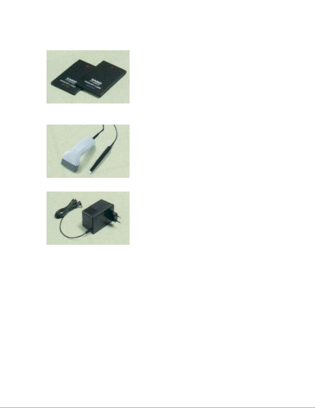
Card
Scanner
AC adaptor
Conforms to the PCMCIA 2.1 standard.
• DT-635MC (S-RAM/256 Kbytes)
• DT-636MC (S-RAM/512 Kbytes)
• DT-637MC (S-RAM/1 Mbyte)
• DT-9031BFMC (F-ROM/4 Mbytes)
• DT-9032BFMC (F-ROM/6 Mbytes)
• DT-9033BFMC (F-ROM/10 Mbytes)
• DT-9034BFMC (F-ROM/20 Mbytes)
• DT-9650BCR (Pen type Bar Code Reader with built-in
decoder)
• DT-9656BCR (Touch type Bar Code Reader with builtin decoder)
• DT-825ADP-U (120VAC, for IT-2060IO-E and IT2065IO-E)
• DT-825ADP-G (230VAC, for IT-2060IO-E and IT2065IO-E)
• DT-9020ADP-U (120VAC, for IT-2000)
• DT-9020ADP-G (230VAC, for IT-2000)
— 4 —
Page 7
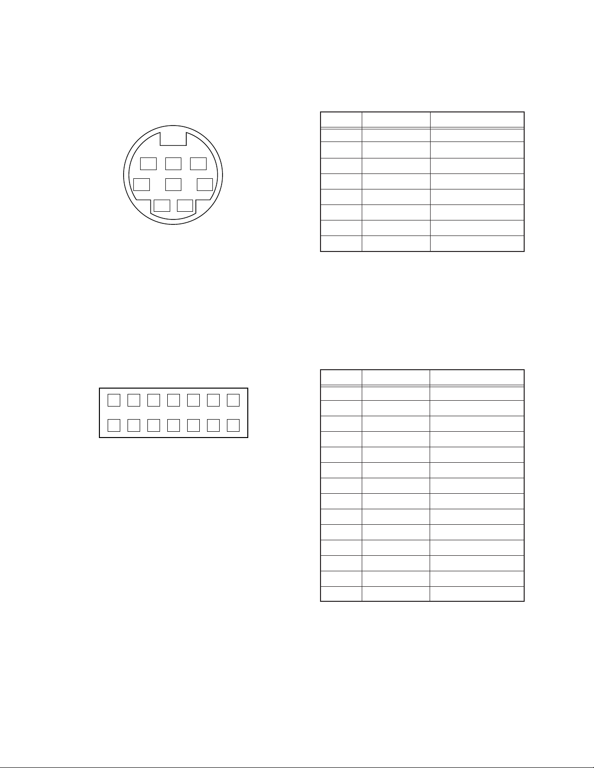
3. INTERFACE PIN ASSIGNMENT
3.1 8 Pin serial I/F
876
543
21
PIN No. Signal Name Description
1 SD Send data
2 RD Receive data
3 RS Request to send
4 CS Clear to send
5 VOUT Power
6 GND Ground
7 ER Equipment ready
8 DR Data set ready
3.2 14 Pin serial I/F (RS-232C)
8 9 10 11 12 13 14
1234567
PIN No. Signal Name Description
1 GND Ground
2 GND Ground
3 NC No Connect
4 SD Send data
5 RD Receive data
6 RS Request to send
7 ER Equipment ready
8 CS Clear to send
9 CI Carrier indicater
10 DR Data set ready
11 CD Carrier detect
12 EXSW External Switch
13 V
14 V
H
H
Power
Power
— 5 —
Page 8
3.3 Card I/F
3.3.1 Memory Card Interface
Memory Card Interface Signals
Pin No. Signal Name I / O Description Pin No. Signal Name I / O Description
1 GND Ground 35 GND Ground
2 D3 I/O Data3 36 CD1# O Card detect1
3 D4 I/O Data4 37 D11 I/O Data11
4 D5 I/O Data5 38 D12 I/O Data12
5 D6 I/O Data6 39 D13 I/O Data13
6 D7 I/O Data7 40 D14 I/O Data14
7 CE1# I Card enable 1 41 D15 I/O Data15
8 A10 I Address10 42 CE2# O Card enable2
9 OE# I Output enable 43 VS1# I 5 V Detect
10 A11 I Address11 44 RFU Reserve
11 A9 I Address9 45 RFU Reserve
12 A8 I Address8 46 A17 I Address17
13 A13 I Address13 47 A18 I Address18
14 A14 I Address14 48 A19 I Address19
15 WE#/PGM I Write enable 49 A20 I Address20
16 RDY/BSY# O Ready/Busy 50 A21 I Address21
17 Vcc Power 51 Vcc Power
18 Vpp1 Programming power1 52 Vpp2 Programming power2
19 A16 I Address16 53 A22 I Address22
20 A15 I Address15 54 A23 I Address23
21 A12 I Address12 55 A24 I Address24
22 A7 I Address7 56 A25 I Address25
23 A6 I Address6 57 RFU Reserve
24 A5 I Address5 58 RESET I Reset
25 A4 I Address4 59 WAIT# O Wait
26 A3 I Address3 60 RFU Reserve
27 A2 I Address2 61 REG# I Atribute memory select
28 A1 I Address1 62 BVD2 O Battery voltage detect2
29 A0 I Address0 63 BVD1 O Battery voltage detect1
30 D0 I / O Data0 64 D8 I/ O Data8
31 D1 I / O Data1 65 D9 I/ O Data9
32 D2 I / O Data2 66 D10 I / O Data10
33 WP O Write protect 67 CD2# O Card detect2
34 GND Ground 68 GND Ground
— 6 —
Page 9

3.3.2 I/O Card Interface
I/O Card Interface signals
Pin No. Signal Name I / O Description Pin No. Signal Name I / O Description
1 GND Ground 35 GND Ground
2 D3 I/O Data3 36 CD1# Card detect1
3 D4 I/O Data4 37 D11 I/O Data11
4 D5 I/O Data5 38 D12 I/O Data12
5 D6 I/O Data6 39 D13 I/O Data13
6 D7 I/O Data7 40 D14 I/O Data14
7 CE1# I Card enable 1 41 D15 I/O Data15
8 A10 I Address10 42 CE2# I Card enable2
9 OE# I Output enable 43 VS1# O 5 V Detect
10 A11 I Address11 44 IORD# I I/O Read
11 A9 I Address9 45 IOWR# I I/O Write
12 A8 I Address8 46 A17 I Address17
13 A13 I Address13 47 A18 I Address18
14 A14 I Address14 48 A19 I Address19
15 WE#/PGM I Write enable 49 A20 I Address20
16 IRE0# O Interrupt request 50 A21 I Address21
17 V c c Power 51 Vc c Power
18 Vpp1 Programming and 52 Vpp2 Programming and
periferal power1 pelipheral power2
19 A16 I Address16 53 A22 I Address22
20 A15 I Address15 54 A23 I Address23
21 A12 I Address12 55 A24 I Address24
22 A7 I Address7 56 A25 I Address25
23 A6 I Address6 57 RFU Reserve
24 A5 I Address5 58 RESET I Reset
25 A4 I Address4 59 WAIT# O Wait
26 A3 I Address3 60 INPACK# O Inputaknolage
27 A2 I Address2 61 REG# I Atribute memory select
28 A1 I Address1 62 SPKR# O Degital Sound signal
29 A0 I Address0 63 STSCHG# O Card status change
30 D0 I/O Data0 64 D8 I/O Data8
31 D1 I/O Data1 65 D9 I/O Data9
32 D2 I/O Data2 66 D10 I/O Data10
33 IOIS16# O 16bit I/O port 67 CD2# O Card detect2
34 GND Ground 68 GND Ground
— 7 —
Page 10

4. SYSTEM DIAGRAM
4.1 System diagram
— 8 —
Page 11

4.2 Block diagram
Battery senser
Tenperature senser
Illuminace senser
— 9 —
Page 12
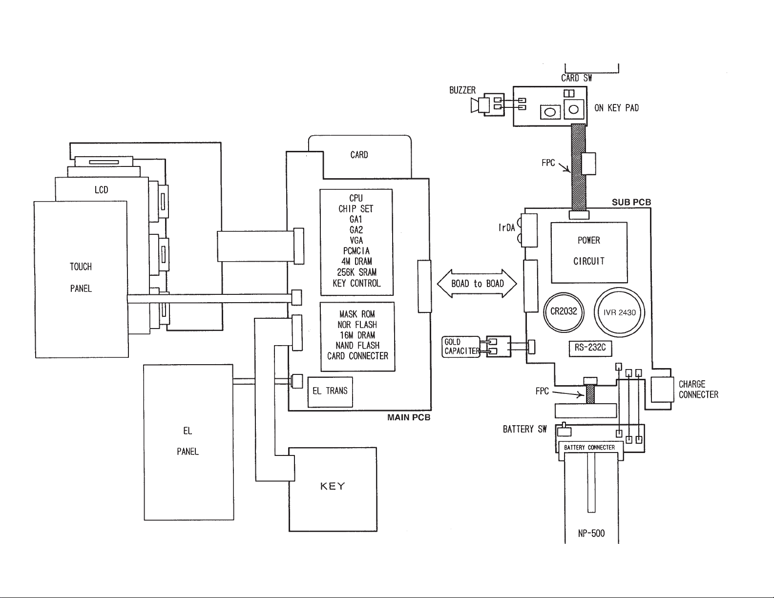
— 10 —
4.3 PCB diagram
ILLUMINACE
SENSOR
8 pin I/F
CONNECTOR
RECHARGE PIN
Page 13
4.4 Power supply diagram
— 11 —
Page 14
5. CIRCUIT DESCRIPTION
5.1 Memory
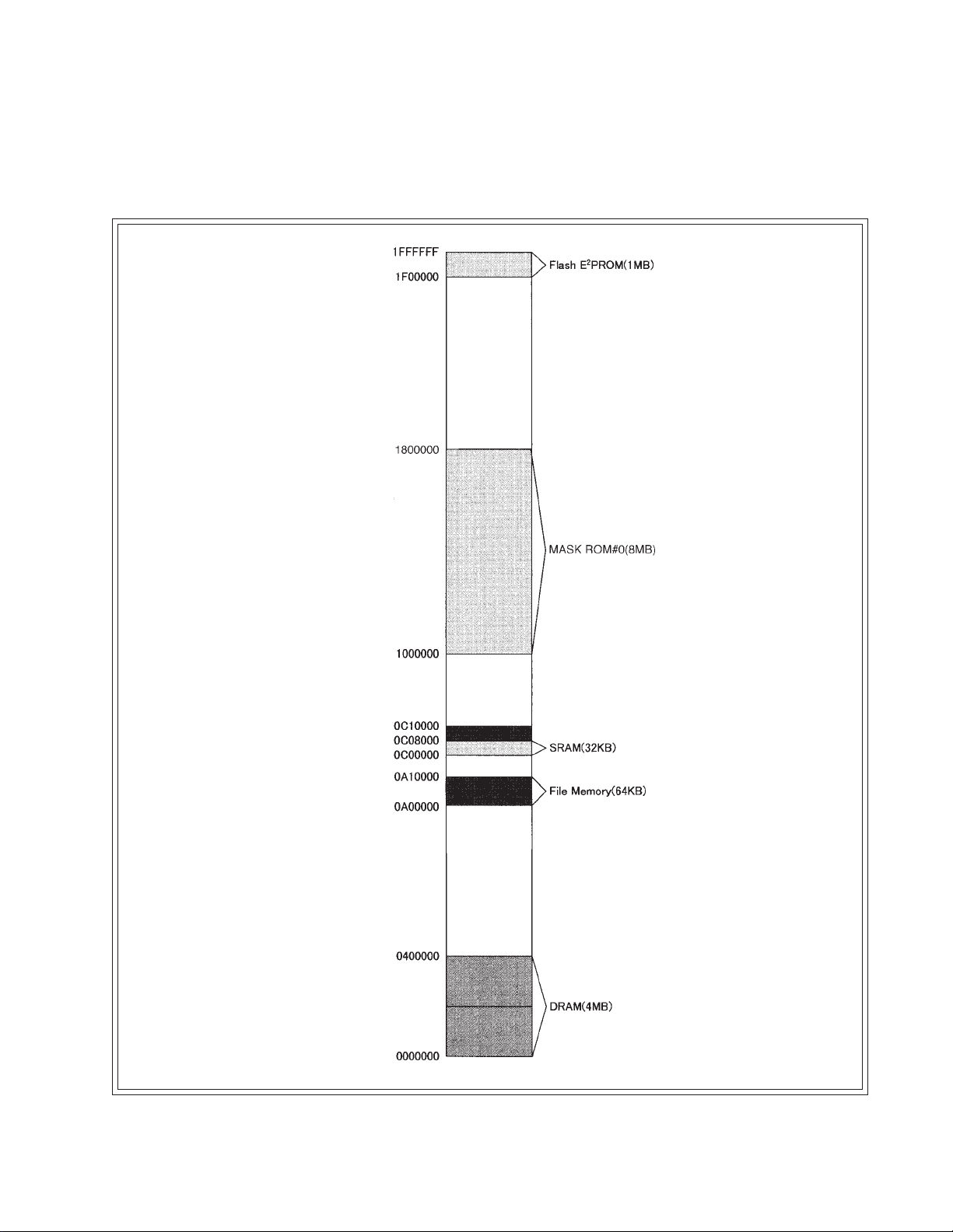
5.1.1 Memory map
Memory map of IT-2000 W30 model is shown in Figure 5.1.1.
Figure 5.1.1 Memory map
— 12 —
Page 15
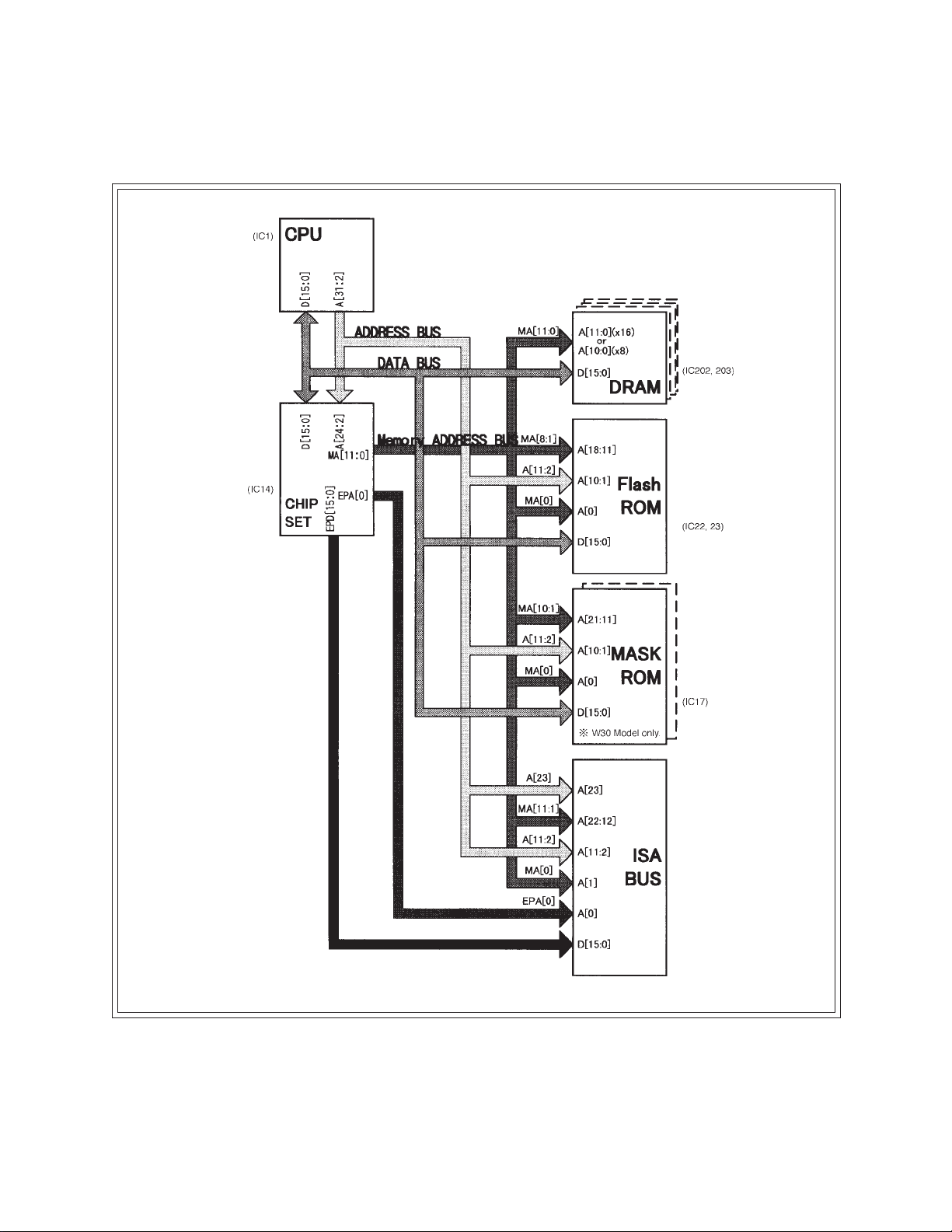
5.1.2 Memory block diagram
Memory block diagram is shown in Figure 5.1.2.
Figure 5.1.2 Memory block diagram
— 13 —
Page 16
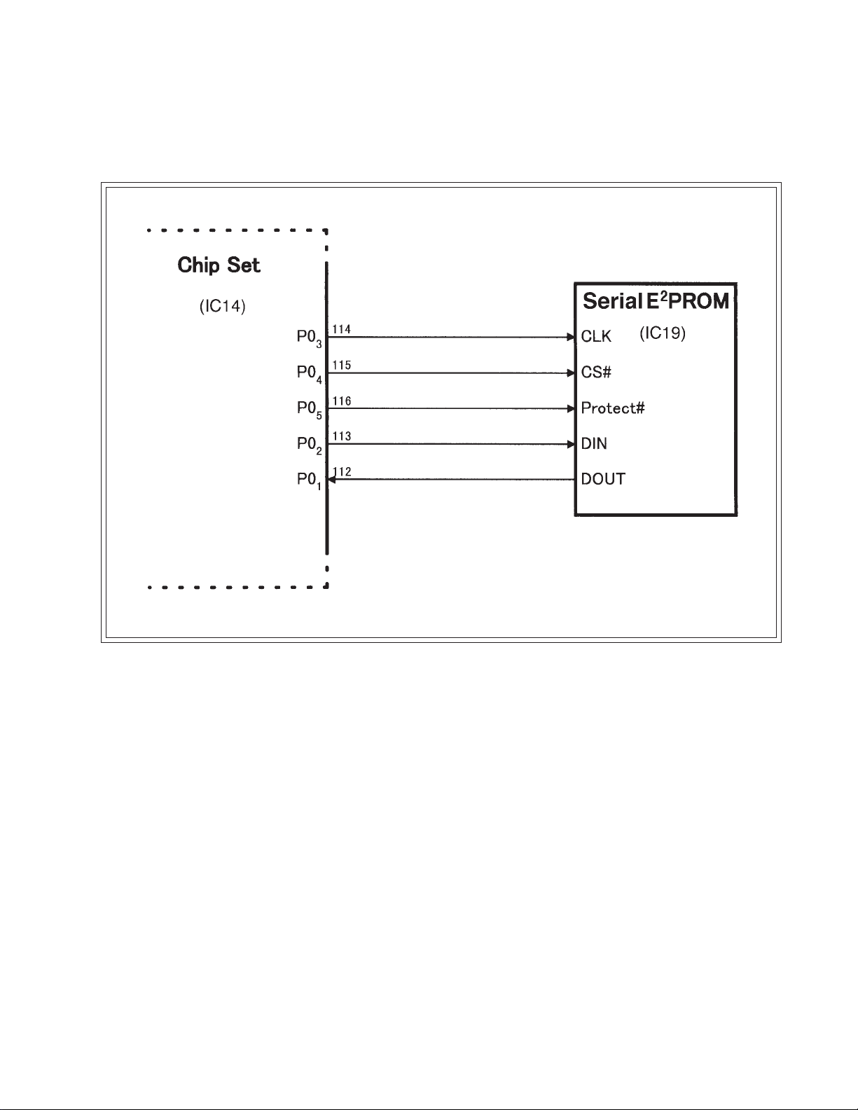
5.1.3 Serial E2PROM
Password and configurations data of the machine are saved in serial E2PROM.
E2PROM diagram is shown in Figure 5.1.3.
Figure 5.1.3 Serial E2PROM
— 14 —
Page 17
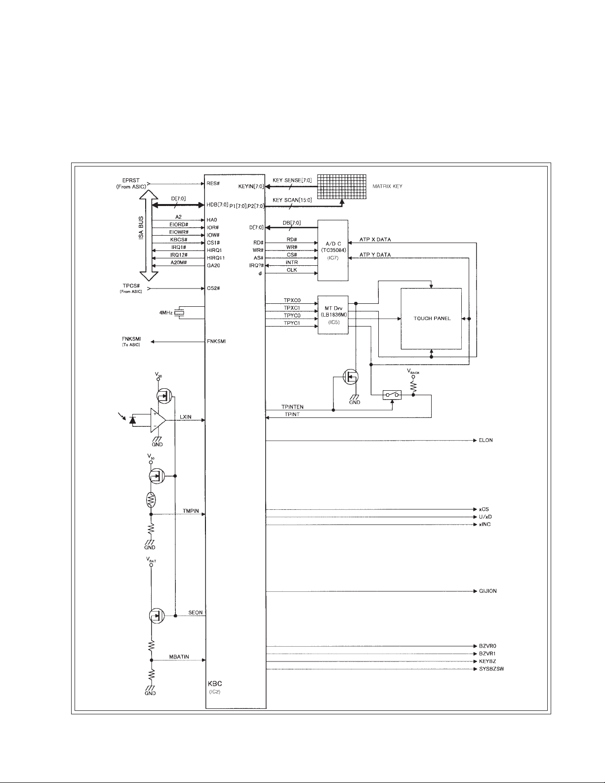
5.2 KBC
5.2.1 KBC block diagram
Input of matrix key and touch panel, LCD contrast, automatic backlight ON/OFF, VBAT monitoring, and
buzzer are controlled at KBC.
KBC diagram is shown in Figure 5.2.1.
Figure 5.2.1 KBC block diagram
— 15 —
Page 18
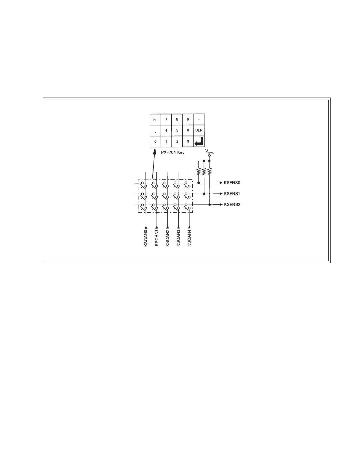
5.2.2 Matrix key
5.2.2.1 Matrix key diagram
Matrix key diagram is shown in Figure 5.2.2.1.
KSENS[2:0] is connected to KEYIN#[2:0] of KBC.
KSCAN[4.0] is connected to a general port of KBC.
Figure 5.2.2.1 Matrix key diagram
— 16 —
Page 19

5.2.2.2 Key Sequence
Interrupt is occurred by pressing the key.
When KBC acknowledges the interrupt, it starts to scan and ends after all SCANS are done once.
Key sequence diagram is shown in Figure 5.2.2.2.
Figure 5.2.2.2 Key Sequence
— 17 —
Page 20
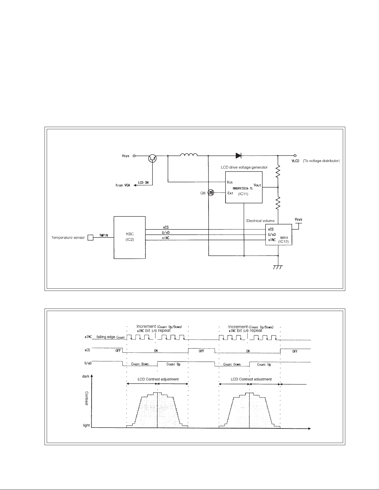
5.2.3 LCD Contrast control
LCD contrast is controlled by KBC.
Use a function of KBC, A/D converter to measure the temperature with a temperature sensor. Then give
the measured data (10 bits AD value) to the system. According to the value system returns the contrast
data to KBC.
KBC adjusts LCD contrast by contrast data.
LCD contrast diagram is shown in Figure 5.2.3.1.
LCD contrast adjustment is shown in Figure 5.2.3.2.
Figure 5.2.3.1 LCD Contrast control diagram
Figure 5.2.3.2 LCD contrast adjustment sequence
— 18 —
Page 21
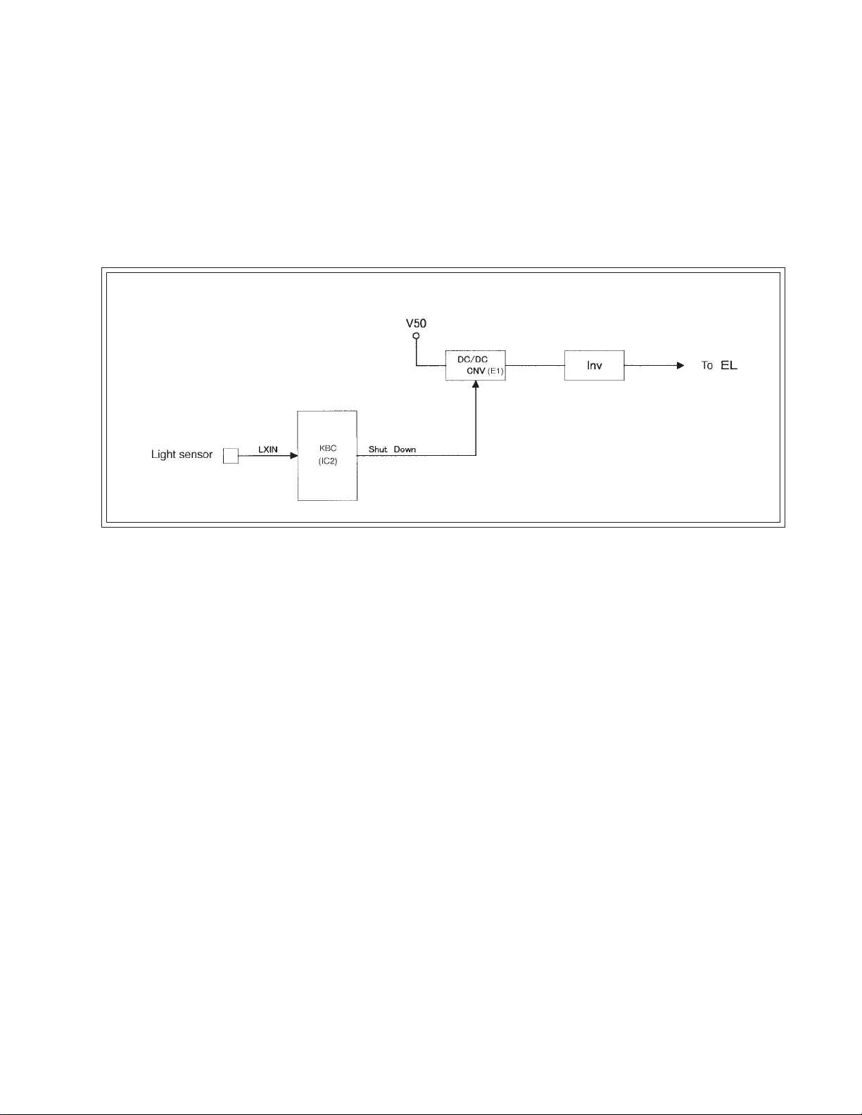
5.2.4 Backlight Control
Backlight is controlled by KBC.
Measure the amount of light with the light sensor.
When light amount falls below a certain amount backlight turns on. When light amount exceeds a certain
amount backlight turns off.
By having a certain amount of hysteresis it prevents the flickering of the backlight.
Backlight control is shown in Figure 5.2.4.
Figure 5.2.4 Backlight Control
— 19 —
Page 22
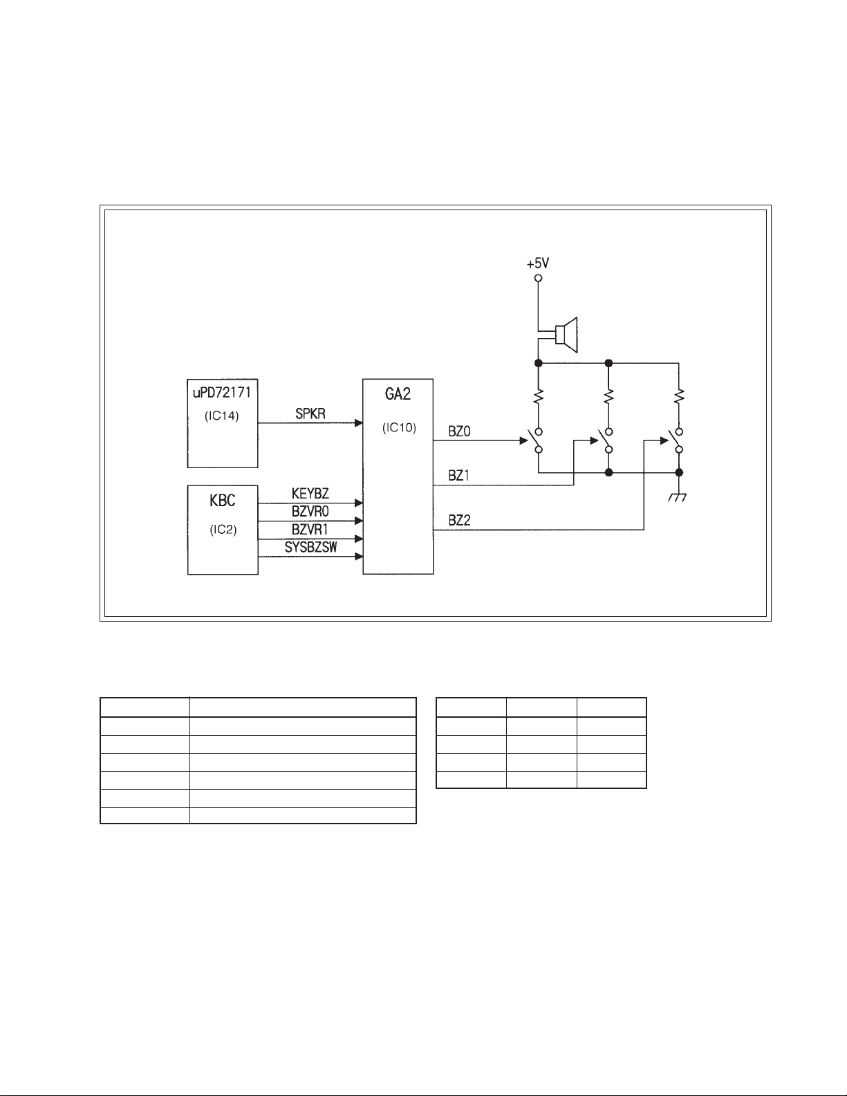
5.2.5 Buzzer Control
KBC controls the volume of the buzzer and the sound of a key click.
Buzzer control diagram is shown in Figure 5.2.5.1.
Buzzer control signal is shown in Chart 5.2.5.2.
Figure 5.2.5.1 Buzzer Control block diagram
Chart 5.2.5.2 Signals controlling buzzer
Signal Function
BZVR0 Controls volume of Buzzer
BZVR1 Controls volume of Buzzer
KEYBZ Controls sound of key click
SYSBZSW Activates system buzzer
SPKR Controls sound of system buzzer
BZ[2:0] Controls volume of Buzzer
BZVR1 BZVR0 Volume
0 0 OFF
0 1 LOW
1 0 Medium
1 1 High
— 20 —
Page 23
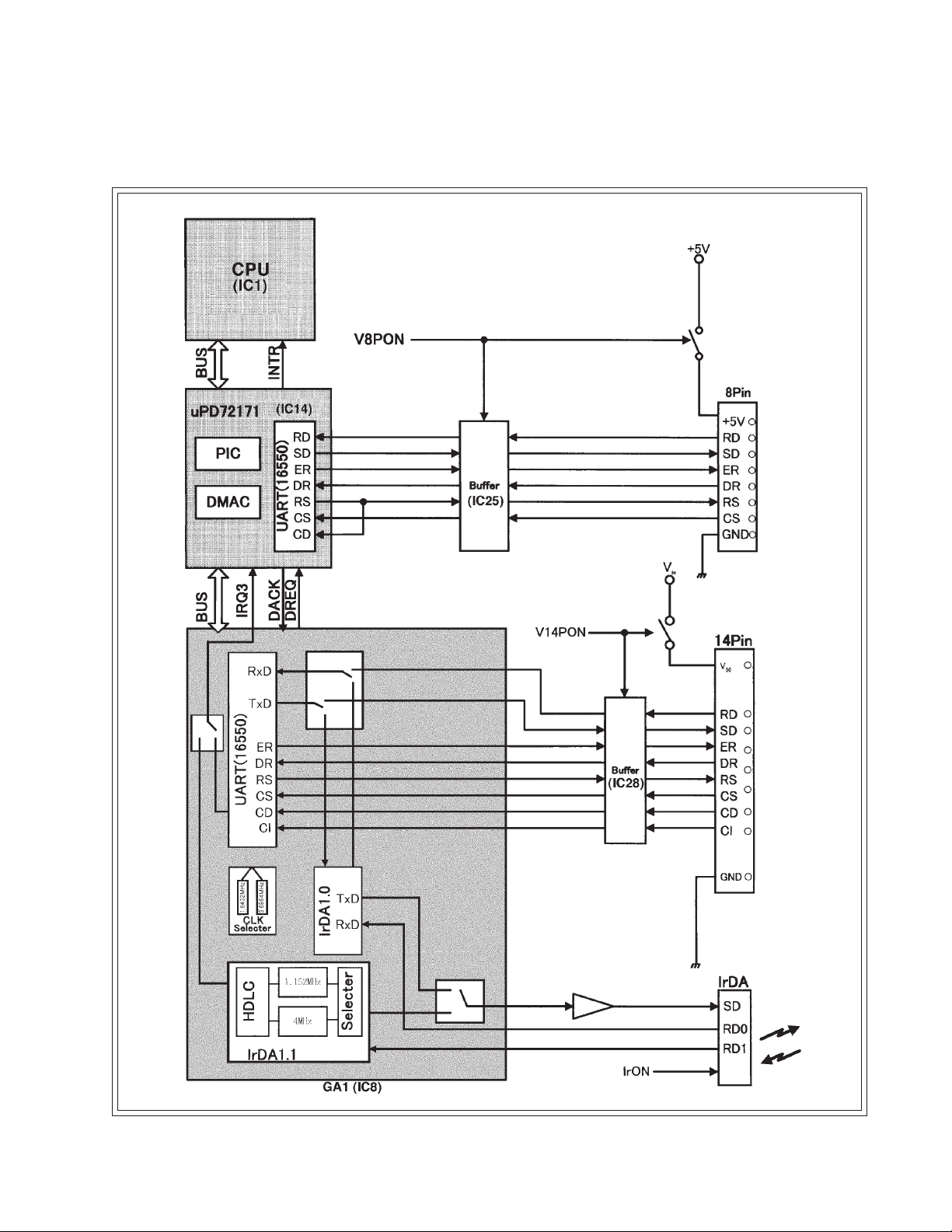
5.3 Communication
Communication block diagram is shown in Figure 5.3.1.
Figure 5.3.1 Communication block diagram
— 21 —
Page 24
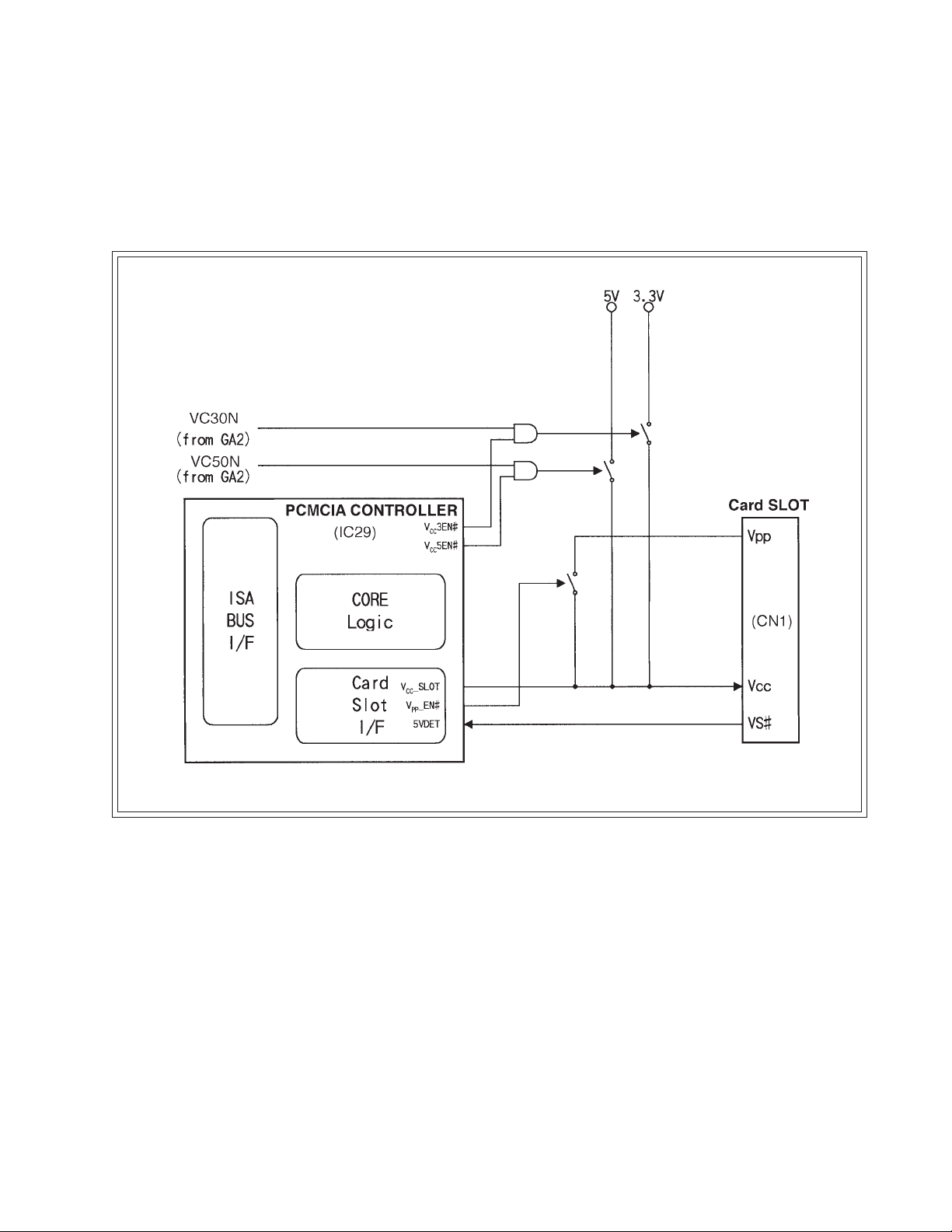
5.4 PC Card
5.4.1 Card power supply circuit
The power supplied to the card is controlled by software.
Card power supply circuit is shown in Figure 5.4.1.
VC5ON, VC3ON, and VCC_SLOT signals control power supply ON/OFF as shown in the diagram.
Figure 5.4.1 Card power supply circuit
— 22 —
Page 25
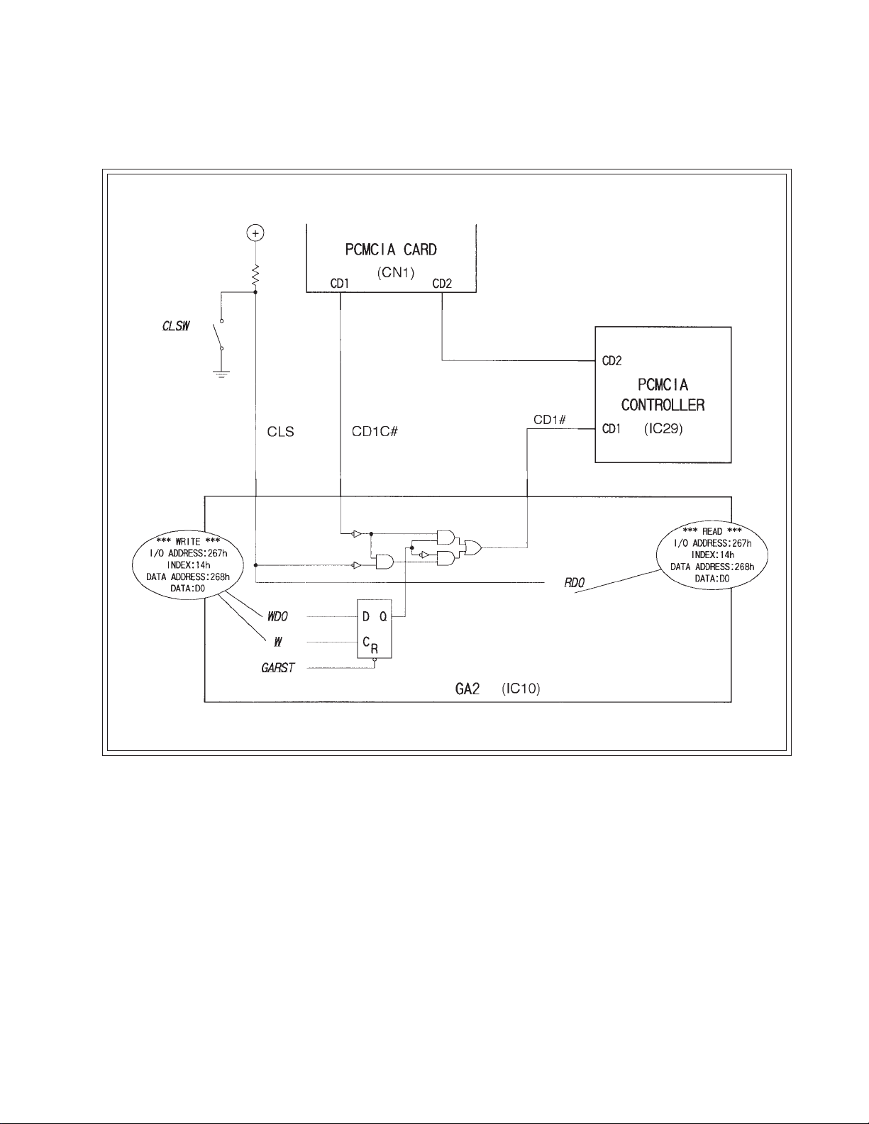
5.4.2 Card lock SW
Card lock SW diagram is shown in Figure 5.4.2.
Figure 5.4.2 Card lock SW diagram
— 23 —
Page 26

5.5 Power Supply
5.5.1 Power specifications
Item
Main battery NP-500 7.2V 1300mA
Backup battery CR-2032 3.0V 210mA
Power Supply block Name Voltage Maximum
Name Application
Vback Chip Set, GA1, GA2, Main memory, VGA Controller, Video memory,
HW Window memory
Vcore CPU (core)
Vsys CPU (I/O), BIOS memory, KBC, MASK-ROM, File memory, PCMCIA
controller
IO
V
50
V
LCD
V
Vcard CARD
IrDA, 8 pin Serial I/F
EL, Buzzer
LCD module
Chart 4-5-1Power specifications
Specification
Name
Voltage
IVR-2430 3.0V 30mA
Vback 3.3V 300mA
Vcore 2.4V 200mA
Vsys 3.3V 300mA
VIO 5.0V 1A
V50 5.0V 500mA
VLCD 30V 30mA
VCARD 3.3V 200mA
5.0V 500mA
Capacity
— 24 —
Page 27

5.5.2 Power transition
This machine is operated by rechargeable lithium battery (main battery) and coin shaped lithium
battery (backup battery). When the main battery power gets low, battery replacement warning is
displayed. When the main battery becomes more weak that it cannot operate the machine, system
turns the power off automatically. Main RAM and RAM disk memory remains due to the backup
battery. The relation between main battery power and the machine is shown as below.
The relation between main battery power and the machine.
Battery power
LB1
LB0
Able to operate
Warning is displayed
Able to turn on power
Turns off antomatically
Starts recharging
Unable to operate
5.5.3 Low battery power monitoring
Monitor the main battery and backup battery. See below for detail.
Name Meaning Detect Voltage Device
LB1 Low main battery power (warning) 6.0 V IC20
LB0 Low main battery power (unable to opelate) 5.5 V IC21
LB2 Low backup battery power (warning) 2.5 V IC3
LB-1 Low backup power (unable to backup) 2.7 V IC13
Able to operate
5.5.4 About power supply
The machine’s power is supplied only from batteries.
When operating the machine while recharging, the machine does not operate from the AC directly
but from the power supplied from the battery that is being recharged.
— 25 —
Page 28

6. DISASSEMBLY
6.1 Removal of the main battery and the backup batteries
1 Slide the open lever to open the battery
pack cover.
2 Remove the main battery.
a M1.7 × 3.8
Open lever
3 Unscrew (a M1.7 × 3.8), then remove the
backup battery cover.
4 Unscrew two screws (b M1.7 × 3.2), then
remove the backup batteries.
6.2 Removal of the battery pack cover
1 Pull the slit in order to remove the battery
pack cover.
6.3 Removal of the Lower case block
1 Unscrew four screws (c M2 × 8).
Battery
Pack
Cover
b M1.7 × 3.2
Slit
e M2 × 12.5
2 Unscrew two screws (d M2 × 6).
3 Unscrew two screws (e M2 × 12.5).
4 Open the lower case by lifting the Card Slot
side.
Card Slot side
d M2 × 6
PRECAUTION
* Since the Upper case block and the Lower case block are connected by FPC Cable do not pull forcibly.
Lower Case
Upper Case
c M2 × 8
— 26 —
Page 29

5 Disconnect two cables from the connectors.
6 Remove the polyester tape.
Polyester tape
(Side view of )
7 Remove the FPC cables by removing the
Adhisive Tape.
Separate the Upper Case Block and the
Lower Case Block.
6.4 Removal of SUB ass’y PCB
1 Remove the connector.
2 Unscrew five screws (f M2 × 4).
3 Separate the BAT ass’y from the
middle case ass’y.
4 Remove the connectors those are hidden
below then remove the SUB ass’y.
FPC cable
BAT A’ssy
connectors
connector
connectors (hidden below)
f M2 × 4
6.5 Disassembly of the Middle Case Block
6.5.1 Removal of the Middle Case ass’y
1 Disconnect two cables from the connectors.
— 27 —
connectors
Page 30

2 Separate the 8 pin serial interface connector
from the Middle Case ass’y.
3 Unscrew four screws (g M2 × 10).
4 Separate the Middle Case ass’y from the
Upper Case.
6.5.2 Removal of the LCD ass’y
g M2 × 10
1 Unscrew two screws (h M2 × 8).
2 Release two stoppers then lift the LCD ass’y.
3 Disconnect two cables from the connectors.
4 Separate the LED ass’y from the Middle
Case ass’y.
stoppers
h M2 × 8
connectors (hidden below)
— 28 —
Page 31

6.5.3 Removal of the MAIN ass’y PCB
1 Pull out ejector lever.
2 Hold and remove the Ejector by pulling
upward.
3 Unscrew five screws (i M2 × 4).
4 Separate the Main ass’y PCB from the
Middle Case.
Ejector
i M2 × 4
6.6 Disassembly of Upper Case Block
6.6.1 Removal of the BZ ass’y and the LUX ass’y
1 Unscrew four screws (j M1.7 × 2.5).
2 Separate the BZ ass’y and the LUX ass’y
from the Upper Case.
6.6.2 Removal of the Key ass’y
1 Unscrew four screws (k M1.7 × 2.5).
2 Separate the Key ass’y from the Upper
Case.
j M1.7 × 2.5
— 29 —
k M1.7 × 2.5
Page 32

7. DIAGNOSTIC PROGRAM
7.1 General
Diagnostic program is made for diagnosing the IT-2000 hardware.
This section shows operating instruction of the diagnostic program with using the Flash ROM card.
7.1.1 Install the diagnostic program to Flash ROM card
1 Prepare for Casio Flash ROM card and the diagnostic disk.
2 Copy all files in the diagnostic disk to Flash ROM card.
Diagnostic disk files are listed in 7.1.4.
Note: Casio Flash ROM card is recommended. If used the other card it may not work normally.
7.1.2 Boot operation
1 Set the Flash ROM card to IT-2000.
2 Press the INIT button.
3 Power turn off after the system menu is displayed.
4 Power turn on again.
5 Select “1. use HIMEM”.
6 Press “1” “1” “9” “ ”.
Test menu appears on the display.
Note: Select “2. Not use HIMEM” in operating IrDA test. IrDA test is not able to execute when
HIMEM is in effect.
7.1.3 Execute the each test
1 Select the test number from the menu on the display and press “ ”.
2 Each test is executed.
When the test is complete it returns to the menu. Otherwise error message will be displayed.
3 To get out of the error display press “CLR”.
Note: Use the matrix key when selecting a number. Touch panel does not work.
— 30 —
Page 33

7.1.4 Diagnostic program files
Diagnostic disk files are listed bellow.
[Diag]
119. bat
Autoexec. bat
Config. sys
Battchk. exe
Bltest. exe
Bztest.exe
Calib. exe
Cardlock. exe
Cardtest. exe
Clktest. exe
Comtest. exe
Crdlswt. exe
Diag_oem. mun
Dinortst. exe
Dispchk. exe
E2ptest .exe
Hwwtest. exe
Ir4mr. exe
Ir4ms. exe
Keytest. exe
Maskrom. exe
Menu. exe
Meter. exe
Nandtst. exe
Penmouse. com
Ramtest1. exe
Ramtest2. exe
Sir2r. exe
Sir2s. exe
Tpin. bat
Tptest. exe
Vramtest. exe
— 31 —
Page 34

7.2 Inspection Detail
Test Menu
1
RAM TEST
2
DINOR FLASH
3
NAND FLASH (except D10 Model)
4
S-E2 PROM
5
G-RAM
6
HW_WINDOW
7
MASK ROM (Windows model
only)
8
LCD TEST
9
8 pin Loop
*Need 8 pin loop back
connecter
10
14 pin Loop
*Need 14 pin I/F tester
Test Detail
Chip Select signal, Address signals, W rite/Read test for DRAM
Chip Select signal, Address signals, Read test for DINOR Flash
Chip Select signal, Address signals, Write/Read test for NAND
Flash
Chip Select signal, Address signals, Read test for Serial
EEPROM
Chip Select signal, Address signals, Write/Read/Verify test for
G–RAM
Chip Select signal, Address signals, Write/Read/Verify test for
HW Window RAM
Chip Select signal, Address signals, Write/Read/Verify test for
MASK RAM
LCD Display test
RS→CS test
ER→DR test
SD→RD test
Check of 8 pin power supply output
1
RS ER CS DR CD CI
000001
010010
100100
111000
SIR Send
11
SIR Receive
12
FIR Send
13
14
FIR Receive
LB TEST
15
CALIB
16
TP Input
17
KEY TEST
18
PC CARD
19
CARD LOCK SW
20
CLOCK
21
BUZZER TEST
22
BL ON
23
BL OFF
24
Batt Meter
25
Temp Meter
26
Bright Meter
27
2 SD→RD test
Infrared Send test (Communication speed:115 kbps)
Infrared Receive test (Communication speed:115 kbps)
Infrared Send test (Communication speed:4 Mbps)
Infrared Receive test (Communication speed:4Mbps)
Check of detection for I/O box, AC adapter, Main battery cover,
Low battery
Touch panel calibration
Touch panel input test
Key test
PCMCIA card test
Card lock switch test
Clock test
Buzzer test
Back light turn on
Back light turn off
Displays battery level
Displays temperature
Displays brightness
— 32 —
Page 35

7.3 Special tool
Special tools are necessary for 8 pin Loop test and 14 pin Loop test.
7.3.1 8 pin loop back connector
Pin No
Signal name
1SD
2RD
3RS
4CS
5VOUT
6 GND
7ER
8DR
8 pin loop back connector wiring is shown in the left.
2KΩ
— 33 —
Page 36

— 34 —
7.3.2 14 pin I/F Tester
14 pin I/F Tester diagram is shown below.
Page 37

7.4 Diagnostic test
<Test Menu Display>
123
PX-704
HARD TEST PROGRAM
Version 1.00
1.
MEMORY
2.
DISPLAY
3.
COMM
4.
POWER
5.
TP & KEY
6.
PC CARD
7.
CLOCK
8.
OTHER
9.
NAND FORMAT
Select “1. MEMORY”
Press “CLR”
Select “2. DISPLAY”
Press “CLR”
PX-704
1. MEMORY
Version 1.00
RAM TEST
1.
DINOR FLASH
2.
NAND FLASH
3.
S-E2 PROM
4.
G-RAM
5.
HW_WINDOW
6.
MASK ROM
7.
4
PX-704
2. DISPLAY
Version 1.00
1.
LCD TEST
Select “1. RAM TEST”
Press “CLR”
PX-704
1. RAM TEST
Version 1.00
1.
Read/Write
2.
Backup T est
5
PX-704
3. COMM
Version 1.00
8 pin Loop
Select “3. COMM”
Press “CLR”
Select “4. POWER” Select “1. LB TEST”
Press “CLR” Press “CLR”
1.
14 pin Loop
2.
SIR Send
3.
SIR Receive
4.
FIR Send
5.
FIR Receive
6.
67
PX-704
4. POWER
Version 1.00
LB TEST
1.
=== Pin Status ===
I/O BOX
CHARGER
Battery SW
M-Batt (LB0)
M-Batt (LB1)
S-Battery
:OFF
:OFF
:OFF
:OFF
:OFF
:OFF
— 35 —
Page 38

18
PX-704
HARD TEST PROGRAM
Version 1.00
1.
MEMORY
2.
DISPLAY
3.
COMM
4.
POWER
5.
TP & KEY
6.
PC CARD
7.
CLOCK
8.
OTHER
9.
NAND FORMAT
Select “5. TP & KEY”
Press “CLR”
Select “6. PC CARD”
Press “CLR”
PX-704
5. TP & KEY
Version 1.00
1.
CALIB
2.
TP Input
3.
KEY TEST
9
PX-704
6. PC CARD
Version 1.00
1.
CARD TEST
2.
CARD LOCK SW
Select “8. OTHER”
Press “CLR”
0
PX-704
HARD TEST PROGRAM
Version 1.00
BUZZER TEST
1.
BL ON
2.
BL OFF
3.
Batt Meter
4.
Temp Meter
5.
Bright Meter
6.
— 36 —
Page 39

RAM TEST
1.
Operation ResultTest menu
Display <Menu 3>.
Fault
<Menu 3>
1. Read/Write
2. Backup Test
2.
DINOR FLASH
Select “1. Read/Write”.
Screen displays as shown
in the right.
Display <Menu 2>.
Select “2. DINOR FLASH”.
Screen displays as shown
in the right.
RAM T esting...
RAM Size = 8192K*
RAM TEST --- OK
Hit Any Key!!
Goes back to Menu 3.
*Varies among models.
<Menu 2>
1. RAM TEST
2. DINOR FLASH
3. NAND FLASH
4. S-E2 PROM
5. G-RAM
6. HW_WINDOW
7. MASK ROM
DINOR Testing...
DINOR TEST ------ OK
Hit Any Key!!
Goes back to Menu 2.
RAM TEST Error
R/W SSSS:AAAA XX YY
SSSS :Segment Address
AAAA :Offset Address
XX :Write Data
yy :Read Data
Press “ ” to return to
Menu 3.
I-FROM Error
AAAA BBBB
AAAA :Correct checksum
BBBB :Calculated
checksum by Read
Data
3. NAND FLASH
D10 Model is
(
not needed.
Display <Menu 1>.
)
Press “ ” to return to
Menu 2.
<Menu 1>
1. MEMORY
2. DISPLAY
3. COMM
4. POWER
5. TP & KEY
6. PC CARD
7. CLOCK
8. OTHER
9. NAND FORMAT
— 37 —
Page 40

Test menu Fault
Operation
Select “9. NAND FORMAT”.
Result
TFORMAT V ersion 3. 3. 3-SP
Copyright c M-Systems,
4. S-E2 PROM
Note:
Caution:Fomatting de-
Display <Menu 2>.
Select “3. NAND FLASH”.
Screen displays as shown
in the right.
Display <Menu 2>.
If NAND-FLASH
is already formatted this operation is not
needed.
letes all files
stored in NAND
FLASH.
Medium physical size is
Boot-image size is 0 Kby
– reserve unit at XXXXX
– reserve unit at XXXXX
– reserve unit at XXXXX
– reserve unit at XXXXX
Finished 12288 Kbytes
Format complete. Formatt
Hit Any Key!!
<Menu 2>
1. RAM TEST
2. DINOR FLASH
3. NAND FLASH
4. S-E2 PROM
5. G-RAM
6. HW_WINDOW
7. MASK ROM
NAND Testing...
NAND Chips – 3.
Disk Size ––– 1 1923456.
NAND Test – OK!
Hit Any Key!!
Goes back to Menu 2.
<Menu 2>
→
It may vary a little
→
When this is displayed
there is no error.
NAND Flash value
→
DISK capacity
Select “4. S-E2 PROM”.
Screen displays as shown
in the right.
1. RAM TEST
2. DINOR FLASH
3. NAND FLASH
4. S-E2 PROM
5. G-RAM
6. HW_WINDOW
7. MASK ROM
E2PROM Testing...
E2PROM TEST – OK
Hit Any Key!!
Goes back to Menu 2.
— 38 —
S-E2 PROM Error
AAAA BBBB
AAAA :Correct checksum
BBBB :Calculated Checksum
by Read Data
Press “ ” to return to
Menu 2.
Page 41

5. G-RAM
Operation ResultTest menu Fault
Display <Menu 2>.
<Menu 2>
1. RAM TEST
2. DINOR FLASH
3. NAND FLASH
4. S-E2 PROM
5. G-RAM
6. HW_WINDOW
7. MASK ROM
6.
HW_WINDOW
Select “5. G-RAM”.
Screen displays as shown
in the right.
Display <Menu 2>.
Select “6. HW-WINDOW”.
Screen displays as shown
in the right.
Vertical Stripes
G-RAM TEST OK
Hit Any Key!!
Goes back to Menu 2.
<Menu 2>
1. RAM TEST
2. DINOR FLASH
3. NAND FLASH
4. S-E2 PROM
5. G-RAM
6. HW_WINDOW
7. MASK ROM
HWW RAM Testing...
HWW RAM TEST - OK
Hit Any Key!!
Goes back to Menu 2.
GRAM Error
XXXX:YYYY AA BB
XXXX :Segment Address
YYYY :Offset Address
AA :Write Data
BB :Read Data
Press “ ” to return to
Menu 2.
HW–WINDOW Error
XXXX:YYYY AA BB
XXXX :Segment Address
YYYY :Offset Address
AA :Write Data
BB :Read Data
7. MASK ROM
Windows
(
model only.
Display <Menu 2>.
)
Press “ ” to return to
Menu 2.
<Menu 2>
1. RAM TEST
2. DINOR FLASH
3. NAND FLASH
4. S-E2 PROM
5. G-RAM
6. HW_WINDOW
7. MASK ROM
— 39 —
Page 42

8. LCD TEST
Operation ResultTest menu Fault
Select “7. MASK ROM”.
MASK ROM Testing...
MASK ROM TEST - OK
Screen displays as
shown in the right.
Hit Any Key!!
Goes back to Menu 2.
XXXX :Segment Address
YYYY :Offset Address
AA :Write Data
BB :Read Data
Press “ ” to return to
Menu 2.
Display <Menu 4>.
<Menu 4>
1. LCD TEST
Select “1. LCD TEST”.
No Display
Screen displays as
shown in the right, then
checks the LCD.
MASK ROM Error
XXXX:YYYY AA BB
Press “ ”.
Press “ ”.
Black
No Display
— 40 —
Page 43

Operation ResultTest menu Fault
Press “ ”.
Press “ ”.
2X patterns
lined up verti-
cally.
Checker
Press “ ”.
Press “ ”.
Reverse
checker
Bars
— 41 —
Page 44

Operation ResultTest menu Fault
Press “ ”.
Reverse bars
Press “ ”.
No display
Press “ ”.
Press “ ”.
Black
No display
— 42 —
Page 45

Operation ResultTest menu Fault
Press “ ”.
LCD TEST ---OK
Hit Any Key!!
Goes back to
Menu 4.
9. 8 pin Loop
*Need 8 pin
loop back
connector.
Connect 8 pin loop back
connector.
Display <Menu 5>
Select “1. 8pin loop” .
Screen displays as
shown in the right.
<Menu 5>
1. 8 pin Loop
2. 14pin Loop
3. SIR Send
4. SIR Receive
5. FIR Send
6. FIR Receive
COM1 CONTROL -- OK
COM1 DATA - OK
Hit Any Key!!
Goes back to Menu 5.
COM1 LINE –
Error Message
NG
COM1 DATA - NG
Error Message
Hit Any Key!!
Error Message
RS ON no Respond
: No response for RS signal
ER ON no Respond
: No response for ER signal
Data not come
: Data unable to transmit
and receive.
Data Error
: Data unmatch
10.14 pin Loop
*Need 14 pin
I/F tester.
Connect the 14 pin I/F
tester.
Display <Menu 5>.
Press “ ” to return to
Menu 5.
<Menu 5>
1. 8 pin Loop
2. 14 pin Loop
3. SIR Send
4. SIR Receive
5. FIR Send
6. FIR Receive
— 43 —
Page 46

Operation ResultTest menu Fault
Select “2. 14pin loop” .
Screen displays as
shown in the right.
COM2 CONTROL -- OK
COM2 DATA - OK
Hit Any Key!!
Goes back to Menu 5.
COM2 LINE –
Error Message
NG
COM2 DATA - NG
Error Message
Hit Any Key!!
Error Message
CI ON no respond
: No response for CI signal
CD ON no respond
: No response for CD signal
DR ON no respond
: No response for DR signal
CS ON no respond
: No response for CS signal
Data not come
: Data unable to tramsmit
and receive.
Data Error
: Communication Data do
not match.
SIR Send
11.
SIR Receive
12.
Display <Menu 5>.
Set the receiving machine
to “4. SIR Receive”.
Select “3. SIR Send”.
✽) Communication
Speed :115 kbps
Display <Menu 5>.
Select “4. SIR Receive”.
<Menu 5>
1. 8 pin Loop
2. 14 pin Loop
3. SIR Send
4. SIR Receive
5. FIR Send
6. FIR Receive
SIR Send Start
Executes IrDA transmission.
Goes back to Menu 5.
<Menu 5>
1. 8 pin Loop
2. 14 pin Loop
3. SIR Send
4. SIR Receive
5. FIR Send
6. FIR Receive
Press “ ” to return to
Menu
5.
SIR Send Start
Rcv Time Out
Hit Any Key!!
The receiving machine
may not have executed “4
SIR Receive”.
— 44 —
Page 47

13.FIR Send
Operation ResultTest menu Fault
Set the transmitting machine to “3. SIR Send”
✽) Communication
Speed :115 kbps
Display <Menu 5>.
Set the receving machine
to “6. FIR Receive”.
SIR Rcv Start
IrDA reception is executed.
Goes back to Menu 5.
<Menu 5>
1. 8 pin Loop
2. 14pin Loop
3. SIR Send
4. SIR Receive
5. FIR Send
6. FIR Receive
SIR Rcv Start
Rcv Time Out
Hit Any Key!!
The transmitting machine
may not have executed “3.
SIR Send”.
14.FIR Receive
15.LB TEST
Select “5. FIR Send”.
✽) Communication
Speed :4 Mbps
Display <Menu 5>.
Select “6. FIR Receive”.
Set the transmitting machine to “5. FIR Send”.
✽) Communication
Speed :4 Mbps
Display <Menu 7>.
FIR send Start
Executes IrDA transmission.
Goes back to Menu Display
5.
<Menu 5>
1. 8 pin Loop
2. 14 pin Loop
3. SIR Send
4. SIR Receive
5. FIR Send
6. FIR Receive
FIR Rcv Start
IrDA reception is executed.
Goes back to Menu 5.
<Menu Display 7>
=== Pin Status ===
FIR Send Start
Rcv Time Out
Hit Any Key!!
The receiving machine
may not have executed “6.
FIR Receive”.
FIR Rcv Start
Rcv Time Out
Hit Any Key!!
The transmitting machine
may not have executed “5
FIR Send”.
I/O BOX
→ I/O BOX.
CHARGER
→ Connecting Adaptor.
I/O BOX :OFF
CHARGER :OFF
Battery SW :OFF
M-Batt (LB0) :OFF
M-Batt (LB1) :OFF
S-Battery :OFF
OFF :not set
ON :set
OFF :disconnected
ON :connected
— 45 —
Page 48

Test menu Fault
Operation
Battery SW
→Main battery cover
Result
OFF :cover is closed
ON :cover is opened
open/close.
M–Batt
→Main battery Low (LB0).
M–Batt
→Main battery Low (LB1).
S–Battry
→Backup battery
OFF :undetected
ON :detected
OFF :undetected
ON :detected
OFF :undetected
ON :detected
(CR2032) Low.
Press CLR key.
Hit Any Key!!
Goes back to Menu6.
16.CALIB
Display <Menu8>.
<Menu 8>
PX-704
5. TP&KEY
Version 1.00
1. CALIB
2. TP Input
3. KEY TEST
17.TP Input
Select “1. CALIB”.
Touch the cross point by
PEN (4 points).
Select “1. EXIT”.
Display <Menu 8>.
✕ ✕
■■ CALIBRATION ■■
Please touch the
cross point by PEN
correctly
1. EXIT
2. RETRY
✕ ✕
Goes back to Menu 8.
<Menu 8>
PX-704
5. TP & KEY
Version 1.00
1. CALIB
2. TP Input
3. KEY TEST
— 46 —
Page 49

Test menu Fault
Operation
Select “2. TP Input”.
Touch the cross point by
PEN (5 points).
Result
✕ ✕
( 0, 0) OFF
Press CLR key.
Goes back to Menu 8.
✕
✕ ✕
Displays each coordinate
figures as you touch them.
While touching, “ON” is
displayed.
After touching all 5 points
display goes back to Menu
8.
18.KEY TEST
Display <Menu 8>.
<Menu 8>
PX-704
5. TP & KEY
Version 1.00
1. CALIB
2. TP Input
3. KEY TEST
Select “3. KEY TEST”.
Input numerical keys (in
any order).
Note: Fn key is recog-
nized by pressing
1 after pressing
[Fn].
Input all keys.
[Fn] [ 7] [ 8] [ 9] [ –]
[ .] [ 4] [ 5] [ 6] [ES]
[ 0] [ 1] [ 2] [ 3] [CR]
The numbers pressed will
become reversed.
KEY TEST --- OK
Hit Any Key!!
When all keys are finished
inputting display goes back
to Menu 8.
— 47 —
Page 50

19.PC CARD
Operation ResultTest menu Fault
Set ATA card. (Formatted)
Display <Menu 9>.
<Menu 9>
PX-704
6. PC CARD
Version 1.00
1. CARD TEST
2. CARD LOCK SW
20.
CARD LOCK SW
Select “1. CARD TEST”.
Set A TA card (formatted),
then turn the CARD
LOCK SW ON.
Display <Menu 9>.
Select “2. CARD LOCK
SW”.
Turn CARD LOCK SW
OFF.
PCMCIA CARD T esting....
CARD Test - OK
Hit Any Key!!
Goes back to Menu 9.
<Menu 9>
PX-704
6. PC CARD
Version 1.00
1. CARD TEST
2. CARD LOCK SW
0=S-LOCK OFF
1=S-LOCK ON
CLR=END TEST
PCIC:ON, Lock Sw:ON
0=S-LOCK OFF
1=S-LOCK ON
CLR=END TEST
21.CLOCK
Press “1”.
Press CLR.
Display <Menu 1>.
PCIC:OFF , Lock Sw:OFF
0=S-LOCK OFF
1=S-LOCK ON
CLR=END TEST
PCIC:ON, Lock Sw:OFF
Goes back to Menu 9.
<Menu 1>
1. MEMORY
2. DISPLAY
3. COMM
4. POWER
5. TP&KEY
6. PC CARD
7. CLOCK
8. OTHER
9. NAND FORMAT
— 48 —
Page 51

22.
BUZZER TEST
Operation ResultTest menu Fault
Select “7. CLOCK TEST”.
1999-12-31 23:59:57
1999-12-31 23:59:58
1999-12-31 23:59:59
2000-01-01 00:00:00
2000-01-01 00:00:01
2000-01-01 00:00:02
2000-01-01 00:00:03
CLOCK TEST --- OK
Hit Any Key !!
Goes back to Menu 1.
Display <Menu 0>.
<Menu 0>
PX-704
HARD TEST PROGRAM
Version 1.00
1. BUZZER TEST
2. BL ON
3. BL OFF
4. Batt Meter
5. Temp Meter
6. Bright Meter
23.BL ON
Select “1. BUZZER TEST”.
Display <Menu 0>.
Select “2. BL ON”.
Three different volume of
buzzer sounds.
BUZ Testing...
BUS TEST --- OK
Hit Any Key!!
Goes back to Menu 0.
<Menu 0>
PX-704
HARD TEST PROGRAM
Version 1.00
1. BUZZER TEST
2. BL ON
3. BL OFF
4. Batt Meter
5. Temp Meter
6. Bright Meter
Backlight turns on.
BL ON is OK
Hit Any Key!!
Goes back to Menu 0.
— 49 —
Page 52

24.BL OFF
Operation ResultTest menu Fault
Display <Menu 0>.
<Menu 0>
PX-704
HARD TEST PROGRAM
Version 1.00
1. BUZZER TEST
2. BL ON
3. BL OFF
4. Batt Meter
5. Temp Meter
6. Bright Meter
25.Batt Meter
Select “3. BL OFF”.
Display <Menu 0>.
Select “4. Batt Meter”.
Backlight turns off.
BL OFF is OK
Hit Any Key!!
Goes back to Menu 0.
<Menu 0>
PX-704
HARD TEST PROGRAM
Version 1.00
1. BUZZER TEST
2. BL ON
3. BL OFF
4. Batt Meter
5. Temp Meter
6. Bright Meter
===== Battery =====
%
AD=XX
100 –
90 –
70 –
60 –
50 –
40 –
30 –
20 –
10 –
0 –
→
Display AD value of battery.
Press CLR.
Press any key.
Indication will vary when 8.4V is seen as 100%.
Hit Any Key !!
Goes back to Menu 0.
— 50 —
Page 53

26.Temp Meter
Operation ResultTest menu Fault
Display <Menu 0>.
Select “5. Temp Meter”.
<Menu 0>
PX-704
HARD TEST PROGRAM
Version 1.00
1. BUZZER TEST
2. BL ON
3. BL OFF
4. Batt Meter
5. Temp Meter
6. Bright Meter
===== Thermometer =====
°C
AD=XX
50 –
40 –
30 –
20 –
10 –
0 –
–10 –
→
Displays AD value of temperature
27. Bright Meter
Press CLR.
Press any key.
Display <Menu 0>.
Shows temperature.
Hit Any Key !!
Goes back to Menu 0.
<Menu 0>
PX-704
HARD TEST PROGRAM
Version 1.00
1. BUZZER TEST
2. BL ON
3. BL OFF
4. Batt Meter
5. Temp Meter
6. Bright Meter
— 51 —
Page 54

Operation ResultTest menu Fault
Select “6. Bright Meter”.
Press CLR.
===== Light Sensor =====
%
AD=XX
100 –
90 –
70 –
60 –
50 –
40 –
30 –
20 –
10 –
0 –
Light level is usually 30~50
in the office.
Hit Any Key !!
→
Displays AD value of sensor.
Press any key.
Goes back to Menu 0.
— 52 —
Page 55

8. CIRCUIT DIAGRAMS
8.1 Curcuit diagram INDEX
PCB Description Drawing No.
MAIN P704-MAIN-1 CPU C341962
P704-MAIN-2 LCD_POWER/EL C341963
KBC C341962
CHIP_SET C341962
GA1 C341962
GA2 C341962
VGA C341962
PCMCIA C341962
DRAM/DINOR-FLASH C341962
MASK-ROM/NAND-FLASH C341962
CONNECTOR C341963
SUB P704-SUB PCB CONNECTER C341827
VBACK/VSYS/VCORE C341827
SUPER_CAP/VCARD C341827
VIO/V50/CHARGE C341827
RS-232C/IrDA C341827
LUX P704-LUX LUX/ON_KEY/BUZZER/CLS C442504
BUZZER P704-BZ BUZZER C442673
CAP P704-CAP SUPER CAPACITOR C442506
BAT P704-BAT BATTERY CONNECTER C442507
KEY P704-KEY KEY C442503
— 53 —
Page 56

A
BCDEFGHI JKLMNOP
1
2
3
4
5
1
2
3
4
5
6
7
8
9
10
6
7
8
9
10
11
Description: Board No. Drawing No.
11
C341962P704-MAIN-1C (1/9)CPU
ABCDEFGH I JKLMNOP
— 54 —
Page 57

A
BCDEFGHI JKLMNOP
1
2
3
4
5
1
2
3
4
(98.2~)
5
6
7
8
9
10
6
7
8
9
10
11
Description: Board No. Drawing No.
11
C341962P704-MAIN-1C (2/9)KBC
ABCDEFGH I JKLMNOP
— 55 —
Page 58

A
BCDEFGHI JKLMNOP
1
2
3
4
5
1
2
3
4
5
6
7
8
9
10
6
7
8
9
10
11
Description: Board No. Drawing No.
11
C341962P704-MAIN-1C (3/9)CHIP_SET
ABCDEFGH I JKLMNOP
— 56 —
Page 59

A
BCDEFGHI JKLMNOP
1
2
3
4
5
1
2
3
4
5
6
7
8
9
10
6
7
8
9
10
11
Description: Board No. Drawing No.
11
C341962P704-MAIN-1C (4/9)GA1
ABCDEFGH I JKLMNOP
— 57 —
Page 60

BCDEFGHI JKA
1
2
3
4
1
2
3
4
5
6
7
8
5
6
7
8
Description: Board No. Drawing No.
C341962P704-MAIN-1C (5/9)GA2
BCDEFGHI JKA
— 58 —
Page 61

A
BCDEFGHI JKLMNOP
1
2
3
4
5
1
2
3
4
5
6
7
8
9
10
6
7
8
9
10
11
Description: Board No. Drawing No.
11
C341962P704-MAIN-1C (6/9)VGA
ABCDEFGH I JKLMNOP
— 59 —
Page 62

A
BCDEFGHI JKLMNOP
1
2
3
4
5
1
2
3
4
5
6
7
8
9
10
6
7
8
9
10
11
Description: Board No. Drawing No.
11
C341962P704-MAIN-1C (7/9)PCMCIA
ABCDEFGH I JKLMNOP
— 60 —
Page 63

A
BCDEFGHI JKLMNOP
1
2
3
4
5
1
2
3
4
5
6
7
8
9
10
DRAM
IC202IC203 IC204IC205
D10 ××
D20 ××
W30 ××
D30P ××
is mounted
is not mounted
×
6
7
8
9
10
11
Description: Board No. Drawing No.
11
C341962P704-MAIN-1C (8/9)DRAM/DINOR-FLASH
ABCDEFGH I JKLMNOP
— 61 —
Page 64

A
BCDEFGHI JKLMNOP
1
2
3
4
5
1
2
3
4
5
6
7
8
9
10
IC26 is not mounted
mounted only on model IC17:W30
NAND-FROM
IC22 IC23 IC24
D10 ×××
D20 ××
W30 ×
D30P ×
is mounted
× is not mounted
6
7
8
9
10
11
Description: Board No. Drawing No.
11
C341962P704-MAIN-1C (9/9)MASK-ROM/NAND-FLASH
ABCDEFGH I JKLMNOP
— 62 —
Page 65

BCDEFGHI JKA
1
2
3
4
1
2
3
4
5
6
7
8
5
6
7
8
Description: Board No. Drawing No.
C341963P704-MAIN-2C (1/2)LCD_POWER/EL
BCDEFGHI JKA
— 63 —
Page 66

A
BCDEFGHI JKLMNOP
1
2
3
4
5
1
2
3
4
5
6
7
8
9
10
6
7
8
9
10
11
Description: Board No. Drawing No.
11
C341963P704-MAIN-2C (2/2)CONNECTOR
ABCDEFGH I JKLMNOP
— 64 —
Page 67

A
BCDEFGHI JKLMNOP
1
2
3
4
5
1
2
3
4
5
6
7
8
9
10
6
7
8
9
10
11
Description: Board No. Drawing No.
11
C341827P704-SUBB (1/5)PCB CONNECTOR
ABCDEFGH I JKLMNOP
— 65 —
Page 68

BCDEFGHI JKA
1
2
3
4
1
2
3
4
5
6
7
8
5
6
7
8
Description: Board No. Drawing No.
C341827P704-SUBB (2/5)VBACK/VSYS/VCORE
BCDEFGHI JKA
— 66 —
Page 69

BCDEFGHI JKA
1
2
3
4
1
2
3
4
5
6
7
8
5
6
7
8
Description: Board No. Drawing No.
C341827P704-SUBB (3/5)SUPER_CAP/VCARD
BCDEFGHI JKA
— 67 —
Page 70

BCDEFGHI JKA
1
2
3
4
1
2
3
4
5
6
7
5
6
7
8
8
Description: Board No. Drawing No.
C341827P704-SUBB (4/5)VIO/V50/CHARGE
BCDEFGHI JKA
— 68 —
Page 71

BCDEFGHI JKA
1
2
3
4
1
2
3
4
5
6
7
8
5
6
7
8
Description: Board No. Drawing No.
C341827P704-SUBB (5/5)RS-232C/IrDA
BCDEFGHI JKA
— 69 —
Page 72

ABCD
1
2
3
1
2
3
4
5
6
4
5
6
Description: Board No. Drawing No.
C442504P704-LUXCLUX/ON_KEY/BUZZER/CLS
ABCD
— 70 —
Page 73

ABCD
1
2
3
1
2
3
4
5
6
4
5
6
Description: Board No. Drawing No.
C442673P704-BZBUZZER
ABCD
— 71 —
Page 74

ABCD
1
2
3
1
2
3
4
5
6
4
5
6
Description: Board No. Drawing No.
C442506P704-CAPBSUPER CAPACITOR
ABCD
— 72 —
Page 75

ABCD
1
2
3
1
2
3
4
5
6
4
5
6
Description: Board No. Drawing No.
C442507P704-BATBBATTERY CONNECTOR
ABCD
— 73 —
Page 76

ABCDEFGH
1
2
3
1
2
3
4
5
6
4
5
6
Description: Board No. Drawing No.
C442503P704-KEYBKEY
ABCDEFGH
— 74 —
Page 77

32
31
29
30
10
9
17
16
14
13
12
33
35
34
4
7
2
5
8
1
5
24
6
23
27
28
25
22
21
26
20
19
18
6
36
15
3
11
9. EXPLODED VIEW
— 75 —
Page 78

10. PARTS LIST
Notes:
1. The numbers in the item column correspond to the same numbers in exploded view.
2. MARKS:
Q: Quantity used per unit
R: Rank
A: Essential
B: Stock recommended
C: Less recommended
X: No stock recommended
— 76 —
Page 79

IT-2000
Item Code No. Parts Name Specification Version Q R
Middle Case Block
1 6541 7808 MAIN ASSY C140528*12 D10 1
1 6541 7809 MAIN ASSY C140528*13 D20 1
1 6541 7803 MAIN ASSY C140528*7 W30 1
1 6541 7810 MAIN ASSY C140528*14 D30P 1
3122 3241 TRANS/INVERTER EBX-542C 1
5860 9989 SCREW 2X8 NI 2 X
6512 6655 PLATE/SHIELD A C341626-1 1 X
6512 6649 INSULATION SEAL B C442227-1 1 X
6512 6928 INSULATION SEAL D C442393-1 1 X
6512 6931 INSULATION SEAL F C442467-1 1 X
IC3 2105 6318 IC/MOS TC75S51FT-TE85L 1
IC6 2105 3388 IC/MOS TC7S66FU-TE85L 1
IC5 2105 5257 IC LB1836M-TE-L 1
IC1 2012 5618 LSI/CPU FA80486GXSF-33 1
IC2 2012 5684 LSI/KBC HD643343VF10 1
IC28 2012 5685 LSI/DRAM HM51W4260CLC7V 1
IC9 2012 5735 LSI/SRAM SRM2B256SLTMX70 1
IC19 2012 5944 LSI HN29WT800T-10-704A 1
IC29 2012 5623 LSI/PCMCIA CONTROLLER RF5C296 1 B
IC15 2012 5687 LSI/SERIAL EEPROM S-29L131AFS-TB 1 B
IC10 2012 5617 LSI/GATE ARRAY SLA908SF3L 1 B
IC27 2012 5625 LSI/VGA CONTROLLER SPC8104F0A 1 B
IC7 2011 7959 LSI TC35084F(TP1) 1 B
IC22 2012 4340 LSI/FLASH-ROM KM29V32000T D20 1 C
IC22,23 2012 4340 LSI/FLASH-ROM KM29V32000T D30P,W30 2 C
IC202,203 2012 5688 LSI/DRAM HM51W17805LTBV-7 2 B
IC8 2012 5626 LSI/GATE ARRAY UPD66346GM-Y00-8ED 1 B
IC14 2012 5627 LSI/CHIP SET UPD72171GD-8EU 1 B
IC25 2101 0251 IC/MOS TC74HC245AF-TP1 1 C
IC16 2105 6359 IC/MOS HD74LVC08TEL 1 C
IC11 2105 6316 IC/MOS RN5RY202A-TL 1 B
IC13 7720 5103 IC/MOS XC61AN2702MR 1 B
IC4 2105 6319 IC/MOS XC62FP4502MR 1 B
IC12 2105 6360 IC X9313WS-3T6 1 B
L3 3841 2165 COIL SLF7032T-150M1R1-2 1 B
J2 3502 2286 CONNECTOR FH12-8S-1SV 1 C
2 CN1 3502 2258 CONNECTOR (PCMCIA) FCN568P06BG/07884E 1 C
J4 3502 1403 CONNECTOR ILZ-7-2PLSMTYE1500 1 C
J3 3502 2259 CONNECTOR FH12-40(19)SA-1SH 1 C
J1 3501 9744 CONNECTOR FH12-7S-1SH 1 C
J5 3502 2287 CONNECTOR KX14-80K8D-E650 1 C
X2 2590 2710 OSCILLATOR/CRYSTAL CX-91F48MHZ-S 1 C
X1 2590 2703 OSCILLATOR/CRYSTAL MA-406-4MHZ 1 C
X3 2590 2711 OSCILLATOR/CRYSTAL MC-306-65.536KHZ 1 C
Q1,3 2259 1596 FET 2SJ204-T1B 2 B
Q6,7,14 2259 2072 FET 2SJ317NY-TR 3 B
Q2,4,5,9,10,11,13, 2254 0336 FET 2SK1580-T1B 10 B
Q200-202
Q8 2250 1583 FET 2SK2054-T1 1 B
R89 2775 3288 RESISTOR/CHIP NETWORK MNR14E0ABJ103 1 X
R1-3,9-16,18,21,24, 2795 7885 RESISTOR/CHIP NETWORK MNR14E0ABJ334 25 X
R41,43,45,48,67-69,
R77,78,93,95
R72-74,79,80 2775 3289 RESISTOR/CHIP NETWORK MNR14E0ABJ472 5 X
— 77 —
A
A
A
A
B
B
B
B
B
B
B
B
B
Page 80

Item Code No. Parts Name Specification Version Q R
R64 2765 2188 POTENTIOMETER/CHIP EVM-3YSX50B24 1 B
L1 3841 1526 INDUCTOR LQH3C4R7M04 1 C
IC17 2012 5883 LSI/MASK ROM D23C64000LGY815MJH W30 1 B
IC200,201,206 2105 6321 IC/MOS TC7S04FU-TE85L 3 B
IC301 2105 5215 IC/MOS TC7W74FU(TE12L) 1 B
3 6540 0227 LCD ASSY C140527*1(HOSYU)F 1 A
4 6514 0300 CASE/MIDDLE C140514-1 1 X
5 6331 6670 SCREW A33953-3 5 X
6 6333 9680 SCREW A33953-9 2 X
7 6514 0308 EJECTOR C341430-1 1
8 6514 0355 INSULATION SEAL C442019-1 1 X
9 6541 7795 BAT ASSY C442063*1 1 C
10 6541 7796 CAPACITOR ASSY C442064*1 1 C
SUB PCB Block
11 6541 7790 SUB ASSY C140529*1 1 A
J7 3501 5103 JACK/POWER HEC3110-01-010 1 C
IC26 2370 1399 IC/HYBRID IRDA RY6FD1SH 1 C
D23 3335 6555 LED BR4361F 1 B
CN1 3501 8358 CONNECTOR (14 pin I/F) A3A-14DA-2SV 1 C
6512 7073 LABEL/CAUTION C442016A-1 1 X
12 6512 8650 SPRING C312171-1 1 C
13 6512 8770 SPRING C413392-1 1 C
14 6511 0770 SPRING/BATTERY C311380-1 1 C
15 6511 0780 SPRING/BATTERY C412183-1 2 C
16 6512 8800 INSULATION SEAL C413399-1 1 X
17 6512 8790 INSULATION SEAL C413398-1 1 X
IC4 2105 6321 IC/MOS TC7S04FU-TE85L 1 B
IC2,5,29 2105 3521 IC/MOS TC7S08FU-TE85L 3 B
IC25,28 2012 5543 IC/MOS MC145583VFEL 2 C
IC3 2105 6322 IC/MOS XC61AC2502MR 1 B
IC6 2105 6361 IC/MOS XC61AC2402MR 1 B
IC19 2105 6324 IC/MOS XC61AN5002MR 1 B
IC21 2105 5649 IC/MOS XC61AN5502MR 1 B
IC200 2105 6362 IC/MOS XC62FP3402MR 1 B
IC20 2105 3724 IC/MOS XC61AN6002MR 1 B
IC9,11 2105 6326 IC/MOS XC62EP2402MR 2 B
IC13 2105 6289 IC/MOS XC62EP3502MR 1 B
IC15,23,24 2105 6327 IC/MOS XC62EP5002MR 3 B
IC18 2105 6328 IC/MOS XC62FP5002MR 1 B
IC7,8 2105 6363 IC/MOS XC6375A341PR 2 B
IC1 2105 6364 IC/MOS XC6382A331MR 1 B
IC10 2105 6365 IC/MOS XC6383B351PR 1 B
IC12 2105 5677 IC/MOS XC6383B601PR 1 B
IC17,22 2116 0119 IC/LINEAR BA10358F-T1 2 B
L1-3 3841 1981 COIL SLF7032T-101MR45-2 3 C
L4,5 3841 2164 COIL SLF7032T-220MR96-2 2 C
J2 3502 2288 CONNECTOR FH12-16S-0.5SH 1 C
J1 3502 2263 CONNECTOR KX-15-80K2D-E1000 1 C
L6 3025 1176 FILTER M-521C 1 C
SW1 3412 2078 SWITCH EVQPLMA15 1 C
R204,205 2795 7885 RESISTOR/CHIP NETWORK MNR14E0ABJ334 2 X
Q23,29,30,35,40,54, 2259 2037 TRANSISTOR 2SA812-T1B(M7) 7 B
Q55
Q16,28,34,52,53 2250 1197 TRANSISTOR 2SB798-T1B 5 B
Q31,24 2253 0679 TRANSISTOR 2SD1628G-TD 2 B
— 78 —
Page 81

Item Code No. Parts Name Specification Version Q R
Q6,10 2259 1953 FET 2SJ203-T1B 2 B
Q1 2259 1596 FET 2SJ204-T1B 1 B
Q14,39 2259 2016 FET 2SJ207-T1B 2 B
Q21,22,27,57,60,62 2259 2072 FET 2SJ317NY-TR 6 B
Q7-9,11,13,17-19,25, 2254 0336 FET 2SK1580-T1B 27 B
Q26,32,36,37,41,42,
Q44-46,48-50,58,59,
Q63-65,200
Q3-5,47,51,56 2254 0266 FET 2SK1582-T1B 6 B
F1 3632 0630 FUSE/CHIP KE10 1 A
R55 2765 2189 POTENTIOMETER EVM-3YSX50B23 1 B
Q12,15 2250 1386 TRANSISTOR 2SA1213(TE12L,C) 2 B
Q20,38 2250 0749 TRANSISTOR 2SA1615-Z-T1 2 X
J6 3501 9149 CONNECTOR/PCB S2B-ZR-SM3A-TF 1 C
IC16 2114 2905 IC/LINEAR M5237ML-T1 1
IC201 2105 6394 IC/MOS TC7SET08FU-TE85L 1
L202-204 3045 0240 INDUCTOR BLM11A121SPT 3
J8 3502 2321 CONNECTOR 52207-0390 1
Q2,43 2254 0556 FET 2SK2090-T1B 2
Upper Case Block
18 6540 0219 CASE ASSY/UPPER C240988*1(HOSYU)A 1
19 6541 7827 BZ ASSY C442066*1 1
20 6541 7828 LUX ASSY C341466*1 1
2390 2177 DIODE/PHOTO BS520 1
21 6512 6635 CABLE/FFC C442165-1 1
3412 2079 SWITCH/PUSH ESE102MH1 1
22 6541 7831 SIF ASSY C442065*1 1
23 6541 7829 KEY ASSY C341464*1 1
24 6541 7830 TOUCH PANEL ASSY C341465*1 1
25 6512 6912 RUBBER/PACKING C441985A-1 1
26 6514 0313 RUBBER/KEY ON C341423-1 1
27 6514 0304 RUBBER/KEY C240504A-4 1
6514 0346 PLATE/BRIND C442005-1 1
28 6514 0297 PEN SUB ASSY C340664*3 1
Lower Case Block
29 6540 0223 CASE ASSY/LOWER C240989*1(HOSYU)B 1
30 6540 0226 CHRGING TERMINAL C240989*1(HOSYU)E 1
31 6514 0332 SHAFT/STRAP C441990-1 2
32 6514 0301 COVER/BATTERY C140515-1 D10,D20,W30 1
32 6514 0302 COVER/BATTERY C140515-2 D30P 1
33 6514 0306 COVER/CARD A C240955-1 D10,D20,W30 1
33 6512 7036 COVER/CARD C C241083-1 D30P 1
33 6512 7034 PACKING/CB-P704SP C442480-1 D30P 1
34 6540 0224 SUB BATTERY ASSY C140525*1(HOSYU)*C 1
35 6540 0225 CN COVER ASSY C140525*1(HOSYU)*D 1
36 6514 0326 CAP/RESET C441983-1 1
B
B
C
B
B
C
C
C
C
C
C
B
C
A
A
C
C
X
A
C
A
A
A
A
C
C
C
B
C
C
— 79 —
Page 82

CASIO TECHNO CO.,LTD.
Overseas Service Division
8-11-10, Nishi-Shinjuku
Shinjuku-ku, Tokyo 160-0023, Japan
 Loading...