

Page 1
fx-7700GE (LX-375)
INDEX
MAR. 1994
(without price)
R
Page 2

CONTENTS
1. SCHEMATIC DIAGRAM
1-1. MAIN BOARD I........................................................................................... 1
1-2. MAIN BOARD II...........................................................................................2
1-3. MAIN BOARD III..........................................................................................3
2. SPECIFICATIONS............................................................................................. 4
3. OPERATION CHECK .........................................................................................5
4. DATA COMMUNICATIONS
4-1. CONNECTING TWO fx-7700GE UNITS ...................................................10
4-2. BEFORE STARTING DATA COMMUNICATIONS...................................11
4-3. SETTING COMMUNICATIONS PARAMETERS ......................................12
4-4. USING ALL TO SEND ALL DATA............................................................13
4-5. USING PROGRAM TO SEND PROGRAM DATA ....................................15
4-6. DATA COMMUNICATIONS PRECAUTIONS...........................................16
5. TROUBLESHOOTING......................................................................................17
6. DISASSEMBLY VIEW......................................................................................18
7. PARTS LIST .................................................................................................... 22
Page 3
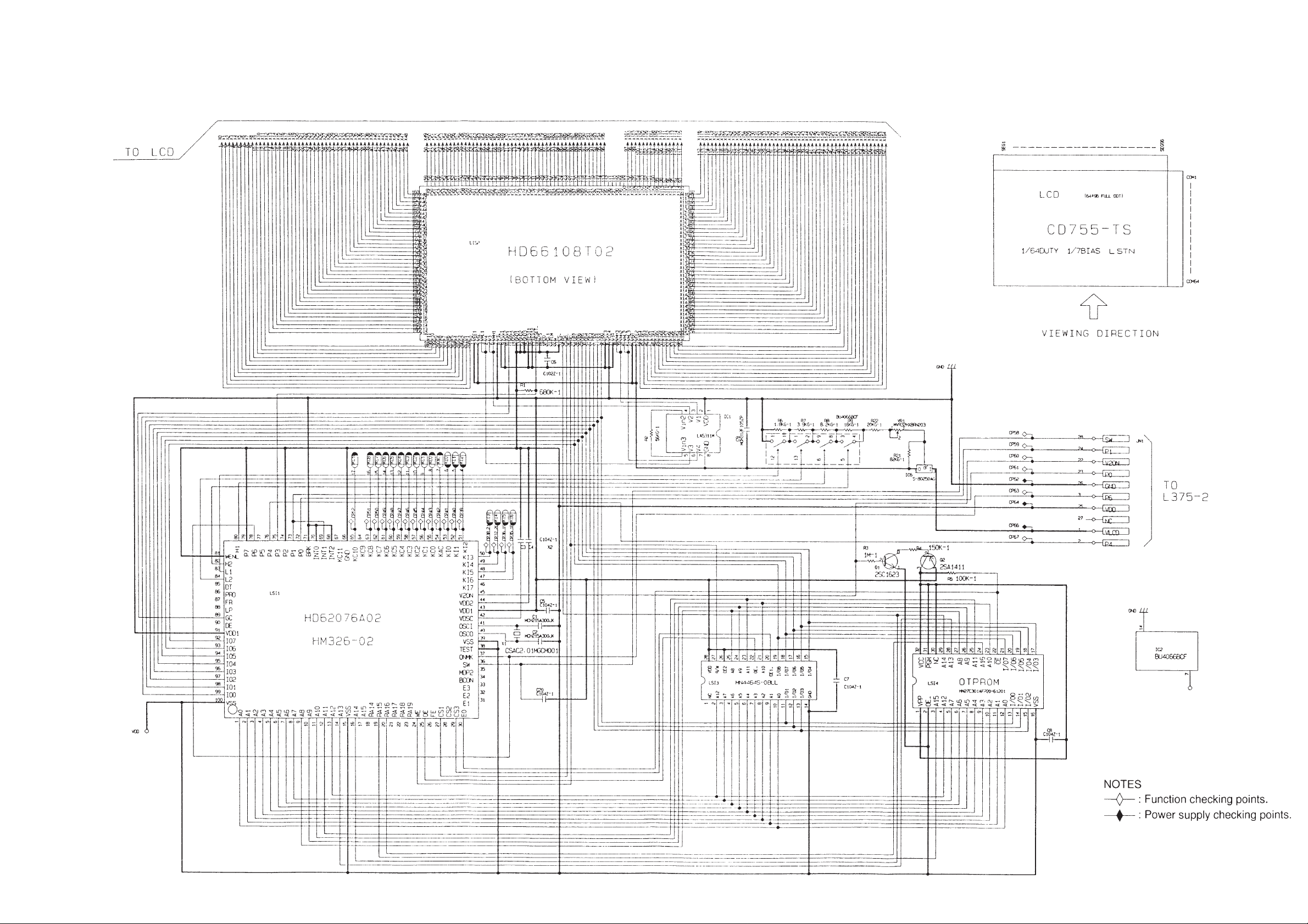
1. SCHEMATIC DIAGRAMS
1-1. MAIN BOARD I
— 1 —
Page 4
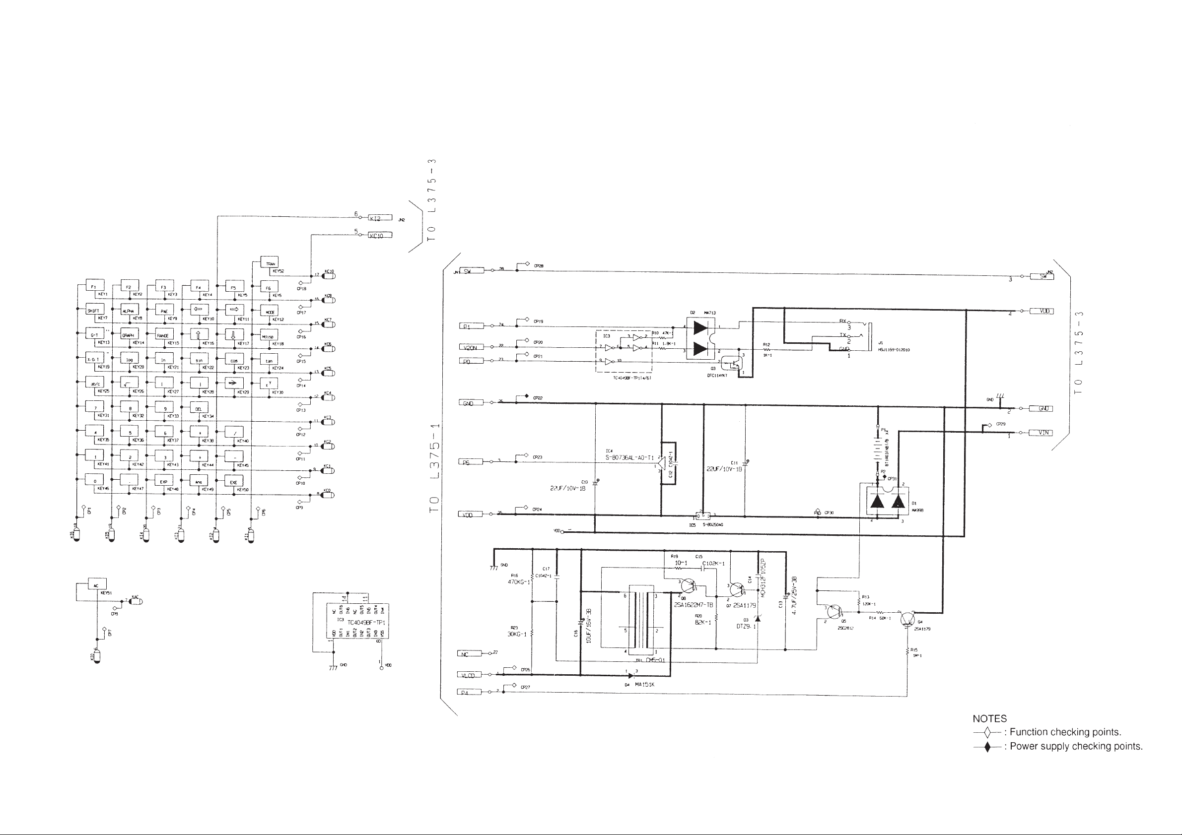
1-2. MAIN BOARD II
— 2 —
Page 5
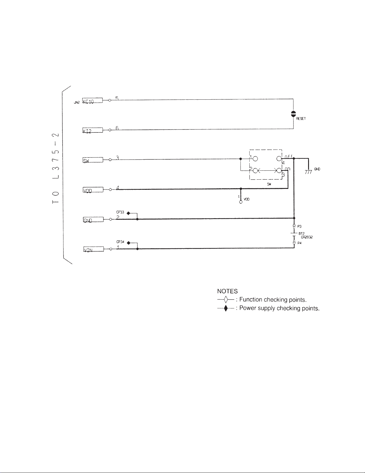
1-3. MAIN BOARD III
— 3 —
Page 6

2. SPECIFICATIONS
Display system: 16-character x 8-line liquid crystal display; 10-digit mantissa and 2-digit expo-
nent for calculations; displays binary, octal, hexadecimal, sexagesimal values,
fraction
Power supply: Main: Four AAA-size batteries (LR03(AM4) or R03 (UM-4))
Memory protection: One CR2032 lithium battery
Power consumption: 0.1W
Battery life: Main: Approximately 350 hours (continuous display of 0) on battery type LR03
(AM4)
Approximately 200 hours (continuous display of 0) on battery type R03
(UM-4)
Approximately 2 years (power switch off) on LR03 (AM4)/R03 (UM-4)
Memory protection: Approximately 1 year
Auto power off: Power is automatically switched off approximately six minutes after last opera-
tion.
Ambient
temperature range: 0°C ~ 40°C (32°F ~ 104°F)
Dimensions: 20mmH x 85mmW x 172.5mmD (3/4"H x 33/8"W x 63/4"D)
Weight: 218.5g (7.7 oz) including batteries
Accessories: Hard Case
CURRENT CONSUMPTION
TYP [µA] MAX [µA]
ON 2673 5147
OFF 15
— 4 —
Page 7
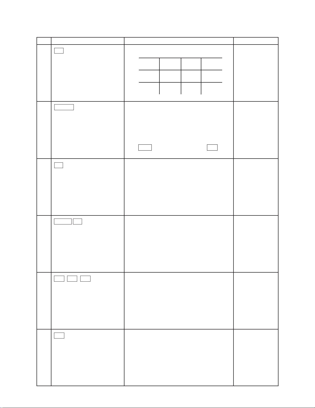
3. OPERATION CHECK
NO. OPERATION DISPLAY NOTE
1
2
3
AC
RESET
F1
MAIN MENU
COMP BASE SD REG
MAT GRAPH EQUA PRGM
LINK CONT
RESET
✽✽✽✽✽✽✽✽✽✽✽✽✽✽✽✽✽✽✽✽
✽
✽✽✽✽✽✽✽✽✽✽✽✽✽✽✽✽✽✽✽✽
RESET ALL MEMORIES?
✽✽✽✽✽✽✽✽✽✽✽✽✽✽✽✽✽✽✽✽
✽
✽
✽
✽
✽
✽
✽✽✽✽✽✽✽✽✽✽✽✽✽✽✽✽✽✽✽✽
RESET
RESET ALLYES NO
RESET
ALL MEMORIES!
✽
✽
✽
✽
✽
✽
✽
SHIFT AC
4
F6 ab/c AC
Press the above keys at the
same time.
5
1
6
No Display
== Lx375 TEST ==
1. LCD 4. ROM
2. KEY 5. TRS
3. RAM 0. rst
No Display
— 5 —
Page 8
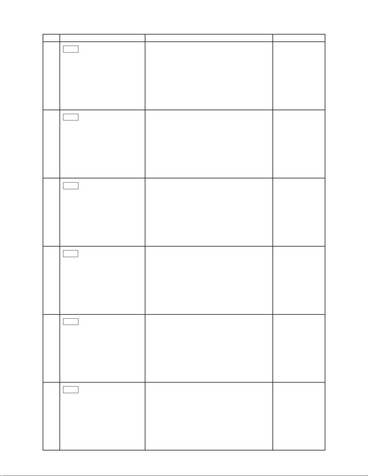
NO. OPERATION DISPLAY NOTE
EXE
7
Checker Display
EXE
8
Reverse checker display
EXE
9
All dot display
10
11
12
EXE
EXE
2
Frame didsplay
== Lx375 TEST ==
1. LCD 4. ROM
2. KEY 5. TRS
3. RAM 0. rst
Trace
— 6 —
Page 9
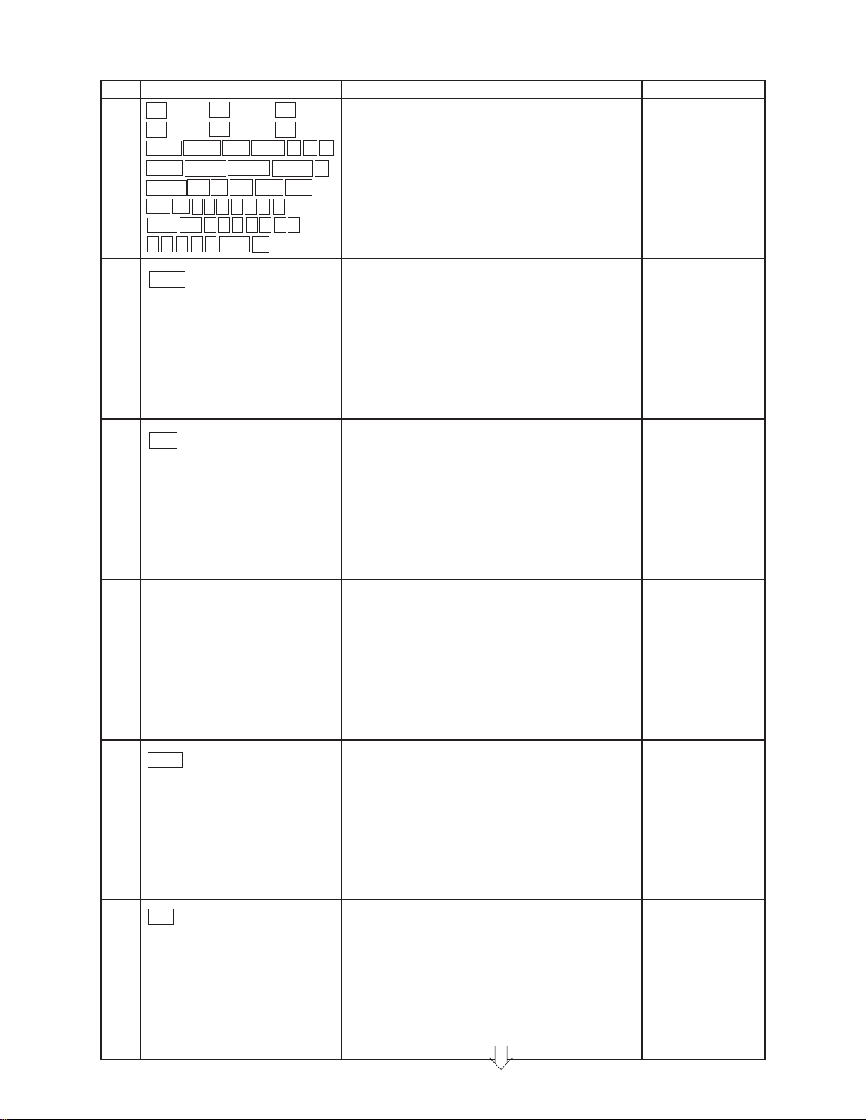
NO. OPERATION DISPLAY NOTE
F1 (Trace)F2 (ZOOM)F3 (Plot)
F4 (Line) F5 (cls) F6 (coord)
SHIFT ALPHA EXIT MENU
G↔T Graph Range MDisp
13
X.Q.T log In Sin Cos Tan
ab/c X2 ( ) ➩ > 8 9
DEL AC 4 5 6 ✕ ÷ 1 2
3 + – 0 . EXP (-)
<
➔
ZOOM Press the key
➔
➔
➔
sequentially
appeared on the
display.
14
15
–
EXE
3
== Lx375 TEST ==
1. LCD 4. ROM
2. KEY 5. TRS
3. RAM 0. rst
...
<< RAM OK >>
A few seconds
after
16
17
EXE
4
== Lx375 TEST ==
1. LCD 4. ROM
2. KEY 5. TRS
3. RAM 0. rst
...
— 7 —
Page 10

NO. OPERATION DISPLAY NOTE
–
EXE
18
Connect the two Lx-375 by
using SB-62.
transfer side
–
receive side
00A6C77D
1. LCD 4. ROM
2. KEY 5. TRS
3. RAM 0. rst
A few seconds
after.
== Lx375 TEST ==
LX-375 LX-375
5
19
1
20
< Set the receive side machine. >
•Operate the in order of
No.1~5.
(21)
•Press the 5 key.
LX-375LX-375
SB-62
TRANSMIT CHECK
1. COM CHECK
2. RANDOM DATA OUT
1. TRANS
2. RECEIVE
1. TRANS
2. RECEIVE
Transfer side
Transfer side
Receive side
— 8 —
Page 11

✽✽✽✽✽✽✽✽✽✽✽✽✽✽✽✽✽✽✽✽
✽
✽
✽
✽
✽
✽
✽✽✽✽✽✽✽✽✽✽✽✽✽✽✽✽✽✽✽✽
RESET
ALL MEMORIES!
✽
✽
✽
✽
✽
✽
NO. OPERATION DISPLAY NOTE
(22)
23
2
DATA RECEIVE
Receive side
TO STOP
PRESS AC KEY
1 Transfer side
TRANSMITTED
<< RECEIVE OK >>
Receive side
EXE
Remove the SB-62.
24
0
25
SHIFT AC
26
== Lx375 TEST ==
1. LCD 4. ROM
2. KEY 5. TRS
3. RAM 0. rst
END
No Display
— 9 —
Page 12

4. DATA COMMUNICATIONS
■ General Procedure
The following is the general procedure to follow when performing data communications. Details of each
procedures are presented in the following sections of this chapter.
• Though you can transfer data between the fx-7700GE and another fx-7700GE, an fx-7700GB or an fx8700GB, all of the examples in this manual cover data transfer with another fx-7700GE only.
1. Connect the two units.
2. Set up the two units with the same parameters.
3. Set up one unit to send, and the other unit to receive.
4. On the receive unit, specify the data to be received and put the unit into receive standby.
5. On the send unit, specify the data to be sent and start the send operation.
4-1. CONNECTING TWO fx-7700GE UNITS
The following procedure describes how to connect two Power Graphic units with an optional SB-62 connecting
cable for transfer of programs between them.
■ To Connect Two fx-7700GE Units
1. Check to make sure that the power of both fx-7700GE units is off.
2. Remove the covers from the connectors of the two Power Graphic units.
• Be sure you keep the connector covers in a safe place so you can replace them after you finish your
program communications.
3. Connect the two units using the SB-62 cable.
SB-62 cable
Important
• Keep the connectors of the fx-7700GE covered when you are not using them.
— 10 —
Page 13

F2
COMMUNICATION
PARITY : EVEN
BPS : 9600
F1: TRANSMIT
F2: RECEIVE
F3: PARAMETERS
TRN
RCV PRM
F1 F2 F6
4-2. BEFORE STARTING DATA COMMUNICATIONS
Before actually starting data communications, you should first enter the LINK Mode from the Main Menu.
■ To Enter the LINK Mode
Highlight the LINK icon on the Main Menu.
MENU
Press
EXE
or to display the LINK Mode.
9
F1
EXE
or
9
F1
The following are the operations that can be selected from the function menu at the bottom of the display. Press
the function key below the operation you want to perform.
F1
(TRN) .............Transmit
F2
(RCV) .............Receive
F6
(PRM).............Parameter settings
■ About the Data Type Selection Screen
Whenever you press F1 (TRN) to send data or F2 (RCV) to receive data, a data type selection screen appears
on the display.
Send Unit Receive Unit
F1
(TRN)
TRANSMIT DATA
ALL
Program
Editor
Function Mem
Matrix
Statistics
Variable Mem
Range
(RCV)
RECEIVE DATA
ALL
Program
Editor
Function Mem
Matrix
Statistics
Variable Mem
Range
Pointer Indicates more below
— 11 —
Page 14

PARAMETERS
TO SELECT : [ ] [ ]
[ ] [ ]
TO SET : [ EXE ]
EVEN
PARITY
EVEN ODD NONE
BPS (x100)
12 24 48 96
The following table describes what each of these items means. You will learn later how to make a selection
using these screens.
Selection Meaning
ALL All data from Program to Equation
Program Program data
Editor File names and file data
Function Mem Function memory contents
Matrix Matrix memory contents
Statistics Single-variable and paired-variable statistical data
Variable Mem Value memory and extended memory contents
Range Graph range parameters
Factor Factor function zoom ratios
Table Table & Graph function data
Graph Function Graph functions
Equation Equation coefficients
Back Up All memory contents, including mode settings
Note
• If the selections you make on the send unit and receive unit do not match, a TRANSMIT ERROR will be
generated on the sender and a RECEIVE ERROR will be generated on the receiver.
4-3. SETTING COMMUNICATIONS PARAMETERS
Before you can perform data communications, you must first set up cartain hardware parameters to make sure
that the two units are able to understand each other. The parameters of the sender and the receiver must be
identical for them to be able to communicate correctly. There are two hardware parameters that you can set.
Parameter Settings
EVEN
Parity ODD
NONE
12(1200)
24(2400)
48(4800)
96(9600)
■ To Set fx-7700GE Parameters
Starting from the LINK Mode:
F6
(PRM)
Speed (BPS)
Pointer
* The parameters that are currently set are highlighted on the display.
— 12 —
Page 15

PARAMETERS
PARITY
EVEN ODD NONE
BPS (x100)
12 24 48
TO SELECT : [ ] [ ]
[ ] [ ]
TO SET : [ EXE ]
NONE
96
COMMUNICATION
PARITY : NONE
BPS : 9600
F1: TRANSMIT
F2: RECEIVE
F6: PARAMETERS
TRN RCV PRM
The pointer indicate which parameter you can change. Use and to move the highlighting and change
the parameter where the pointer is located.
Use and to move the pointer up and down.
After the parameters are highlighted the way you want, press
EXE
EXE
to store them.
• To abort the parameter setting procedure and return the settings to what they were before you changed
them, press AC before pressing
EXE
to store the parameters.
4-4. USING ALL TO SEND ALL DATA
The following procedures show how to send all data, from Program to Equation from one fx-7700GE unit
to another.
•Warning!
The following operation causes data in the seven applicable memory areas (program, function memory,
matrix memory, single-variable and paired-variable statistical data memory, value and extended
mempry, graph function memory, and equation coefficient memory) of the receiving unit to be replaced
by the received by the received data. Make sure that you do not need the data stored in the receiving
unit before you start this operation.
— 13 —
Page 16

RECEIVE DATA
ALL
Program
Editor
Function Mem
Matrix
Statistics
Variable Mem
Range
• To send ALL data
F2
F1
= = RECEIVING = =
ALL DATA
TO STOP : [ AC ]
COMMUNICATION
COMPLETE
ALL DATA
PRESS [ AC ]
Send Unit
Starting from the LINK Mode, press the function key
to enter the send mode.
F1
(TRN)
TRANSMIT DATA
ALL
Program
Editor
Function Mem
Matrix
Statistics
Variable Mem
Range
Make sure that the pointer is located at ALL, and
EXE
press
EXE
to specify it as the data type.
= = TRANSMIT = =
ALL DATA
YES
NO
Receive Unit
Starting from the LINK Mode, press the function key
to enter the receive mode.
(RCV)
Make sure that the pointer is located at ALL, and
EXE
press
EXE
to specify it as the data type.
= = RECEIVE = =
ALL DATA
YES
NO
F1 F6
Press F1 (YES) to start the send operation, or
F6
(NO) to abort without sending anything.
F1
(YES)
= = TRANSMITTING = =
ALL DATA
TO STOP : [ AC ]
* Pressing AC interrupts the send operation and
returns to the LINK Mode.
The following appears after the send operation is
complete.
COMMUNICATION
COMPLETE
ALL DATA
PRESS [ AC ]
F1 F6
Press F1 (YES) to start the receive operation, or
F6
(NO) to abort without receiving anything.
(YES)
* Pressing AC interrupts the receive operation and
returns to the LINK Mode.
The following appears after the receive operation is
complete.
* Press AC to return to the LINK Mode.
— 14 —
Page 17

4-5. USING PROGRAM TO SEND PROGRAM DATA
F6
= = RECEIVING = =
BACK UP
TO STOP : [ AC ]
= = RECEIVE = =
PROGRAM
F1 F2
ONEALL
= = RECEIVE = =
BACK UP
YES
NO
F1 F6
The following procedures show how to send program data from one fx-7700GE unit to another. You can
specify one specific program or all programs for the communication operation.
• To send all PROGRAM data
Send Unit
Starting from the LINK Mode, press F1(TRN) to enter
the send mode.
Move the pointer to Program, and press
EXE
to
specify it as the data type.
EXE
= = TRANSMIT = =
PROGRAM
ALL ONE
F1 F2
• To back up all data
Send Unit
Starting from the LINK Mode, press F1(TRN) to enter
the send mode.
Receive Unit
Starting from the LINK Mode, press F2(RCV) to
enter the receive mode.
Move the pointer to Program, and press
EXE
to
specify it as the data type.
EXE
Receive Unit
Starting from the LINK Mode, press F2(RCV) to
enter the receive mode.
Move the pointer to Back Up, and press
specify it as the data type.
EXE
Press F1 (YES) to start the send operation, or
F6
(NO) to abort without sending anything.
F1 (YES)
* Pressing AC interrupts the send operation and
returns to the LINK Mode.
= = TRANSMIT = =
BACK UP
YES
F1 F6
= = TRANSMITTING = =
BACK UP
TO STOP : [ AC ]
EXE
NO
to
Move the pointer to Back Up, and press
EXE
to
specify it as the data type.
EXE
Press F1 (YES) to start the send operation, or
(NO) to abort without receiving anything.
F1 (YES)
*Pressing AC interrupts the receive operation and
returns to the LINK Mode.
— 15 —
Page 18

The following appears after the send operation is
COMMUNICATION
COMPLETE
BACK UP
PRESS [ AC ]
complete.
COMMUNICATION
COMPLETE
BACK UP
PRESS [ AC ]
The following appears after the receive operation is
complete.
* Press AC to return to the LINK Mode.
4-6. DATA COMMUNICATIONS PRECAUTIONS
Note the following precautions whenever you perform data communications.
• A TRANSMIT ERROR occurs whenever you try to send data to a receiving unit that is not yet standing by
to receive data. When this happens, press AC to clear the error and try again, after setting up the receiving
unit to receive data.
• A RECEIVE ERROR occurs whenever the receiving unit does not receive any data approximately six
minutes after it is set up to receive data. When this happens, press AC to clear the error.
• A TRANSMIT ERROR or RECEIVE ERROR occurs during data communications if the cable becomes
disconnected, if the parameters of the two units do not match, or if any other communications problem
occurs. When this happens, press AC to clear the error and correct the problem before trying data
communications again. In this case, any data received before the problem occurred is cleared from the
receiving unit's memory.
• A MEMORY FULL operation occurs if the receiving unit memory becomes full during data communications.
When this happens, press AC to clear the error and delete unneeded data from the receiving unit to make
room for the new data, and then try again.
— 16 —
Page 19

5. TROUBLESHOOTING
SYMPTOM CAUSE SOLUTION
Intermittent display
No display at all
Erratic display
Dirt or poor contact on battery
Poor contact on power switch
Poor connection on PC joiner
Poor soldering on LSI, capacitor, or resistor
Weak battery
Dirt or poor contact on battery
Poor contact on power switch
Poor connection on PC joiner
Defective LSI, capacitor, or resistor
Poor contact between LCD and PCB
Poor soldering on LSI
Clean or adjust pressure of
contact
Clean or replace power
switch
Resolder or replace
Resolder
Replace battery
Clean or adjust pressure of
contact
Clean or replace power
switch
Resolder or replace
Replace
Replace the heat seal
Resolder or replace display
PCB ass'y
Certain key does not
function
All keys do not function
Heavy key motion
Dirt on key contact
Heavy key motion
Poor soldering on LSI
Defective LSI, capacitor, or resistor
Constant contact is made on a certain key
Defective LSI, capacitor, or resistor
Dirt or scratch on the key
Clean or replace contact
Clean or replace the key
Resolder
Replace
Separate the contact
Replace
Clean or replace the key
— 17 —
Page 20

6. DISASSEMBLY VIEW
— 18 —
Page 21

— 19 —
Page 22

— 20 —
Page 23

— 21 —
Page 24

7. PARTS LIST
FOB Japan
N Item Code No. Parts Name Specification Q M N.R.Yen R
Unit Price
L375-1 ASS'Y
LSI1 2011 0105 LSI HD62076A02 1 1 C
LSI2 2011 1239 LSI HD66108T02 1 1 C
N LSI3 2010 7259 LSI MN4464S-08LL 1 1 C
N LSI4 2011 7280 LSI HN27C301AFP20-61201 1 1 C
IC1 2189 2009 Linear IC LA5311M-TP-T1 1 1 C
N IC2 2105 3213 C-MOS IC BU4066BCF-T1 1 10 C
N IC6 2105 2982 MOS IC S-80250AG-GB-T1 1 5 C
X1 2590 0777 Ceramic oscillator CSAC2.01MGCM001-TC 1 1 C
C1/C2 2845 2499 Chip capacitor MCH215A300JK 2 20 C
C3/C4/C5/C6 2845 1540 Chip capacitor MCH212F104ZK 7 20 C
C7/C8/C20
C9 2845 1925 Chip capacitor MCH312F105ZP 1 10 C
R1 2795 1309 Chip resistor MCR10EZHJ684 1 10 C
R2 2795 3262 Chip resistor MCR10EZHG563 1 20 C
R3 2795 0532 Chip resistor MCR10EZHJ105 1 20 C
R4 2792 0977 Chip resistor MCR10EZHJ154 1 10 C
R5 2792 0209 Chip resistor MCR10EZHJ104 1 20 C
R6 2795 2450 Chip resistor MCR10EZHG182 1 20 C
N R7 2795 0504 Chip resistor MCR10EZHG392 1 20 C
N R8 2730 0622 Chip resistor MCR10EZHG822 1 20 C
N R9 2795 4956 Chip resistor MCR10EZHG163 1 20 C
R21 2795 2184 Chip resistor MCR10EZHG823 1 20 C
N R22 2795 3836 Chip resistor MCR10EZHG203 1 20 C
Q1 2252 0112 Chip transistor 2SC1623-T1B(L6,L7) 1 1 C
N Q2 2250 0413 Chip transistor 2SA1411-T1B(M16) 1 20 C
N VR1 3122 1862 Chip volume MVR32HXBRN203 1 20 C
N 1 5610 7660 Heat seal A-L375 A313350-1 1 1 B
N 2 5610 7670 Heat seal B-L375 A313351-1 1 1 B
N 3 6408 0490 Tape A-L375 A414163-1 1 20 X
4 6405 9090 Tape D-L373 A413732-1 3 20 X
N 5 6408 0450 LCD holder L375 A211376-1 1 20 C
N 6 6407 9930 Flat screw A-L370 A310044-41 1 20 C
N 7 6409 2950 Adhesive tape B-L375 A414588-1 2 20 C
8 6405 9110 Adhesive tape C-L373 A412118-2 2 20 C
N 9 3335 4711 LCD CD777-TS 1 1 C
N 10 6409 2960 PC joiner B-L375 A413642-4 1 5 C
N 13 6408 0410 L375-2 ass'y A211385*1 1 1 C
(This unit contains the above parts as it's element)
N 11 6408 0380 L375-1 ass'y A110928A*1 H 1 1 A
(This unit contains the above parts as it's element)
L375-2 ASS'Y
IC3 2101 0952 MOS IC TC4049BF-TP1 1 1 C
N IC4 2105 3220 CMOS IC RH5VL36CA-T1 1 10 C
N IC5 2105 2982 MOS IC S-80250AG-GB-T1 1 5 C
N C10/C11 2803 6687 Electrolytic capasitor 10RE2-22-T58-T 2 20 C
C12/C17 2845 1540 Chip capacitor MCH212F104ZK 2 20 C
N C13/C16 2803 6701 Electrolytic capacitor 25RC2-4R7-T58-T 2 20 C
C14 2845 1925 Chip capacitor MCH312F105ZP 1 10 C
N C15 2845 4711 Chip capacitor MCH215C152KK 1 20 C
N TR1 3841 1183 Chip coil CM5-01 1 5 C
D1 2390 1407 Chip diode MA998-(TX) 1 10 C
Notes: N – New parts R – A : Essential
M – Minimum order/supply quantity B : Stock recommended
R – Rank C : Others
Q – Quantity used per unit X : No stock recommended
— 22 —
Page 25

FOB Japan
N Item Code No. Parts Name Specification Q M N.R.Yen R
Unit Price
D2 2390 0364 Schottky diode MA713-TX 1 10 C
N D3 2360 2247 Zenner diode DTZ9.1BTT11 1 20 C
D4 2301 2359 Chip diode MA151K-(TX) 1 20 C
R10 2792 0462 Chip resistor MCR10EZHJ473 1 20 C
R11 2792 1191 Chip resistor MCR10EZHJ182 1 10 C
R12 2792 0470 Chip resistor MCR10EZHJ102 1 20 C
R13 2730 0547 Chip resistor MCR10EZHJ124 1 20 C
R15 2795 0532 Chip resistor MCR10EZHJ105 1 20 C
N R16 2730 0583 Chip resistor MCR10EZHG474 1 20 C
R19 2792 0926 Chip resistor MCR10EZHJ100 1 20 C
R14 2795 0742 Chip resistor MCR10EZHJ683 1 20 C
R20 2792 0462 Chip resistor MCR10EZHJ473 2 20 C
N R23 2795 0518 Chip resistor MCR10EZHG153 1 20 C
Q3 2259 0959 Chip digital transistor DTC114YKT-146 1 20 C
N Q4/Q7 2250 0826 Chip transistor 2SA1179M6,M7-TB 2 20 C
Q5 2221 0378 Chip transistor 2SC2812-L5,L6-TB 1 20 C
N Q8 2250 0833 Chip transistor 2SA1622-M7-TB 1 20 C
J1 3501 6538 Miniature jack HSJ1169-012010 1 5 C
N 12 6408 0480 PC joiner L375 A413642-2 1 10 C
N 13 6408 0410 L375-2 ass'y A211385*1 1 1 C
(This unit contains the above parts as it's element)
LOWER CASE ASS'Y
N 14 6408 0440 Lower case L375 A110919-1 1 1 C
N 15 6408 0010 Battery spring A-L375 A311808-3 1 20 C
N 16 6407 9950 Battery spring B-L375 A310154-3 1 20 C
N 17 6408 0460 Switch knob L375 A313343-1 1 10 C
N 18 6408 0100 Battery spring A-L370 A410112-3 1 20 C
N 19 6408 0110 Battery spring B-L370 A410113-3 2 20 C
N 20 6408 0120 Battery spring L370 A412218-2 1 20 C
N 21 6408 0170 CushionA-L370 A413632-1 3 20 C
22 6391 8831 Reset key V160 A311024A-1 1 20 C
23 6274 7023 Contact spring A4532C-1 1 10 C
N 24 6408 0091 Battery spring A-L375 A33938-3 1 20 C
25 6405 9260 Nut L373 A411430-3 1 20 C
26 6405 9240 Battery insuration plate L373 A413729-1 1 20 C
27 6405 9250 Insuration seal L373 A413730-1 1 20 C
28 6405 6440 Blind L171 A413625-1 1 20 C
COMPONENT
N 29 6407 9961 Battery cover L375 A310945A-3 1 20 C
N 30 6408 0470 Display plate L375 A313345-1 1 5 C
N 31 6408 0220 Rubber foot L375 A413646-1 1 20 C
N 32 6408 0430 Upper case L375 A110918-1 1 1 C
N 33 6408 5190 Button A-L375 A211169-2 1 10 C
N 34 6408 5210 Button B-L375 A211316-2 1 10 C
N 35 6408 0030 Button C-L370 A312937-1 1 20 C
N 36 6408 5200 Button D-L375 A211172-2 1 20 C
N 37 6408 0070 Button E-L370 A313257-1 1 20 C
N 38 6408 0080 Button F-L370 A313257-2 1 20 C
N 39 6408 5220 Button G-L375 A311693-13 1 20 C
N 40 6408 5230 Button H-L375 A311693-14 1 20 C
N 41 6408 5240 Button I-L375 A311693-15 1 20 C
N 42 6408 5250 Button J-L375 A311639-16 1 20 C
N 43 6408 0020 Button K-L370 A312914-1 1 10 C
Notes: N – New parts R – A : Essential
M – Minimum order/supply quantity B : Stock recommended
R – Rank C : Others
Q – Quantity used per unit X : No stock recommended
— 23 —
Page 26

FOB Japan
N Item Code No. Parts Name Specification Q M N.R.Yen R
Unit Price
N 44 6407 9880 Key contact rubber L370 A211181-1 1 5 C
N 45 6407 9900 Hard case L370 A211187-1 1 5 C
N 46 6407 9910 Battery cover L370 A211188-1 1 20 C
N 47 6407 9930 Flat screw A-L370 A310044-41 6 20 C
N 48 6407 9940 Flat screw C-L370 A310044-43 5 20 C
N 49 6408 0060 Battery cover L370 A312944-1 1 20 C
N 50 6408 0200 Label L370 A413640-1 1 20 X
51 6390 0431 Cap V332 A310765A-1 1 20 B
52 6405 8860 Decoration screw C-L373 A412299-6 1 20 C
53 6405 8780 Tape E-L373 A411085-3 1 20 X
N 54 6409 4270 Cushion B-L375 A414576-1 3 20 C
N 55 6409 2940 Cushion C-L375 A414577-1 1 20 C
Notes: N – New parts R – A : Essential
M – Minimum order/supply quantity B : Stock recommended
R – Rank C : Others
Q – Quantity used per unit X : No stock recommended
— 24 —
Page 27

8-11-10, Nishi-Shinjuku
Shinjuku-ku, Tokyo 160, Japan
Telephone: 03-3347-4926
 Loading...