

Page 1
SERVICE MANUAL
FE-700
INDEX
(without price)
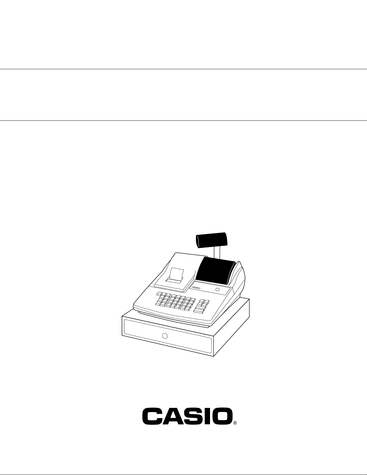
ELECTRONIC CASH REGISTER
FE-700 MEX (EX-287 Mexican Version)
Jan. 2003
0.00
0.00
(without price)
F
E
-7
0
0
Printer model : M190G
Page 2

CONTENTS
FE-700 Page
1. SPECIFICATIONS........................................................................................ 1
2. INITIALIZE (MAC) OPERATION.................................................................. 2
3. F-INIT (FMAC) OPERATION ....................................................................... 2
4. BLOCK DIAGRAM....................................................................................... 3
4-1. PCB CONNECTION.............................................................................. 3
4-2. BLOCK DIAGRAM (CIRCUIT).............................................................. 4
5. DISASSEMBLY (FE-700)............................................................................. 5
5-1. MAIN PARTS ........................................................................................ 5
6. CIRCUIT EXPLANATION ............................................................................ 8
6-1. Power supply circuit ........................................................................... 8
6-2. CPU (IC11: uPD78052GC-A46-8BT) ................................................... 9
6-3. Display controller (IC2: uPD16312GB-3B4)..................................... 11
6-4. Initilize IC (Reset circuit)................................................................... 12
6-5. Power down detection circuit (PWD)............................................... 12
6-6. Address latch circuit ......................................................................... 12
6-7. RAM / ROM / Fiscal ROM bank selection circuit............................. 13
6-8. Fiscal ROM address and data selection.......................................... 14
6-9. Head drive circuit for printer ............................................................ 15
6-10. VPP sensor circuit........................................................................... 16
6-11. Power supply circuit for display ................................................... 17
7. DIAGNOSTIC ............................................................................................. 18
7-1. To start the diagnostic program ...................................................... 18
7-2. Check item ......................................................................................... 18
7-3. Operation of each test....................................................................... 18
7-4. Switch status test .............................................................................. 19
7-5. Individual function test ..................................................................... 20
7-6. Fiscal ROM test.................................................................................. 23
7-7. To exit the diagnostic test ................................................................ 23
8. ERROR CODE ........................................................................................... 24
8-1. Operation error code......................................................................... 24
8-2. Fiscal ROM error code ...................................................................... 25
8-3. System lock code .............................................................................. 26
9. IC DATA ..................................................................................................... 27
10. PCB LAYOUT ............................................................................................ 32
11. CIRCUIT DIAGRAM ................................................................................... 33
12. PARTS LIST............................................................................................... 50
Page 3
1. SPECIFICATIONS
Power consumption In operation Max 30W
Memory protection Backup battery Vanadium Lithium secondary battery
Memory capacity 1Mbits uPD431000ACZ-70LL
Clock and calender Accuracy Within ±30 sec. per month(25˚C)
Environment Operating temperature 0°C ~ 40°C
Printer Model M-190G(071)
Standby 11W
Mode SW OFF 7W
VL3032/1F2
Back up period 90 days (25°C)
Battery life 5 years (25°C)
Recharge time 48 hours
Auto calender Effective until 2099 A.D.
Operating humidity 10% ~ 90%
Storage temperature -25°C ~ 65°C
Storage humidity 10% ~ 95%
Print method Dot matrix printing
MCBF 1,500,000 lines
Life 2,500,000 lines
(Motor,Head unit,Cam trigger set, etc.)
Ink cassette Model ERC-40P
Life About 2,000,000 charactors
Roll paper Type Fine-quality paper
or Pressure-sensitive copy paper
Size 57.5±0.5 mm
Roll diameter 80 mm or less
Paper thickness Upper : 0.066mm
Lower : 0.058mm
— 1 —
Page 4
2. INITIALIZE (MAC) OPERATION
1. Set the mode switch to "OFF" position.
2. Press the "INIT SW".
3. Turn the mode switch to ""REG" (Except "OFF" or "Z") position.
4. Release the "INIT SW" .
5. Input the MAC CODE. (10 digits)
6. Press "#2" key.
7. Initialize operation is executed.
MAC CODE : D1 to D10 (10 digits)
D1 to D6 : Date input data (DD-MM-YY) Note: YY= 00 (2000) to 99 (2099)
D7 to D9 : Any number input digit.(exp : 000)
D10 :select figure break point symbol (1:"." , 2: "," )
NOTE: In case the ECR works abruptly caused cange ROM without removing the battery,
Turn the power off and remove the battery connector then perform the MAC operation.
3. F-INIT (FMAC) OPERATION
1. Set the mode switch to "OFF" position.
2. Press the "INIT SW" .
3. Turn the mode switch to "REG" (Except "OFF" or "Z") position.
4. Release the "INIT SW".
5. Press "#2" key.
Note : The location of "#2" key, see "HARD KEY CODE TABLE" on page 18.
— 2 —
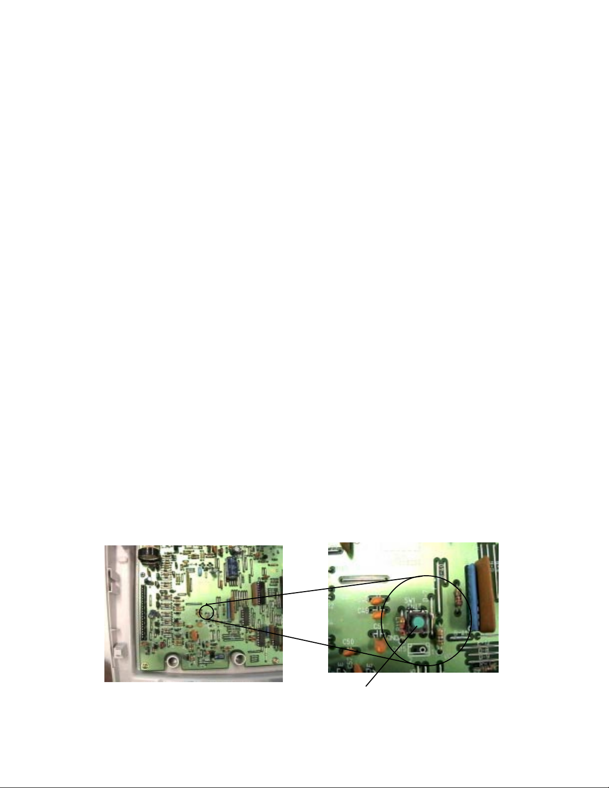
INIT SW
Page 5

4. BLOCK DIAGRAM
4-1. PCB CONNECTION
— 3 —
Page 6
4-2. BLOCK DIAGRAM (CIRCUIT)
Reset circuit
Printer
M190G
S80719AN
MD
FD
Head drive cuicuit
HD.A~HD.H
PWD detection
CPU
uPD78052G-A46-8BT
A8~A15
AD0~AD7
CUSTOMER DISPLAY
SH101MA
Sensor signal
DI,DO,CLK,STB
A0~A7
uPD16312GB-3B4
Select addess
AD0~AD5
MAIN DISPLA
SH101MAY
Segment & Digit data
DRWS
PNES
KC0~KC4
Keyboard
FPC
Mode
Key
VPP sensor circuit
RS232C circuit
ROM
RAM
A0~A7
A8~A15
FB0~FB5
FISCAL ROM
D0~D7
Address data bus
AD0~AD7
— 4 —
Page 7
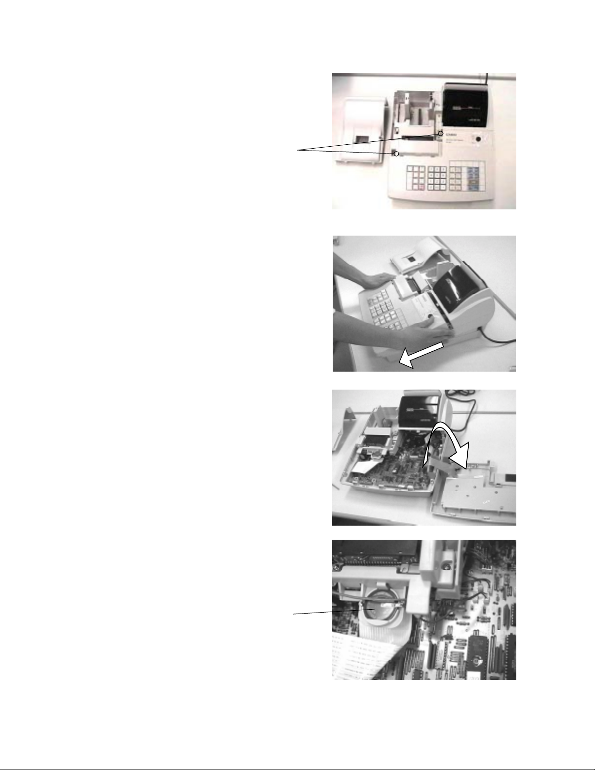
5.DISASSEMBLY (FE-700)
5-1.MAIN PARTS
1.Open the printer cover.
Remove the 2 screws of the upper case.
Remove the 2 screws.
2.Slide the upper case to the front side.
3.Open upper case from the left side.
4.The battery is located at the printer fixing stand.
Battery VL3032/1F2
— 5 —
Page 8
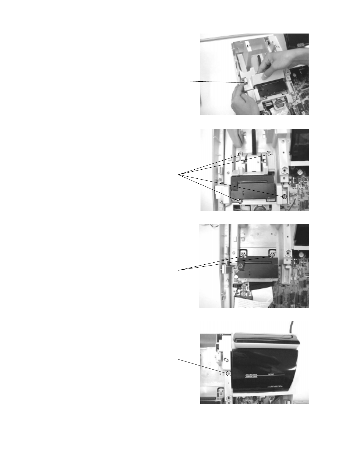
5. Release the hook them Remove the write side.
Hook
6. Release 3screws to remove printer plastic stand.
Remove the 4 screws.
7. Release 2screws to remove printer unit.
Remove the 2 screws.
8. Release 1 screw to remove display case.
Remove 1 screw.
— 6 —
Page 9
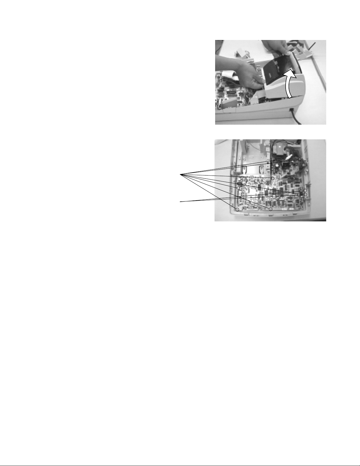
9. Lift up upper case.
10. To remove the main PCB, release 7 screws and
2 screws for the COM port.
Remove the 7 screws.
Remove the 2 screws for the COM port.
— 7 —
Page 10
6.CIRCUIT EXPLANATION
6-1. Power supply circuit
Q1 : Power transistor
Q2 : Voltage detection transistor
A
B
C
D
Voltage level at above check point (unit : V )
Measurement
position
Voltage (V) 12.5V 5.3V 6.2V 2 .47V
AB CD
— 8 —
Page 11

6-2. CPU (IC11: uPD78052GC-A46-8BT)
Pin No. Signal Description In/Out
1 FB3 Fiscal ROM bank 3 Out High High
2 FB4 Fiscal ROM bank 4 / RAM bank 3 Out High High
3 FB5 Fiscal ROM bank 5 / RAM bank 4 Out High High
4 AVSS GND - GND GND
5 PGM PRG signal for Fiscal ROM Out High High
6 RAM RAM disable Out High Low
7 AVREF VDD - 5V 5V
8 RXD Receive data In High High
9 TXD Send data Out High High
10 WD Winder motor drive signal Out Low Low
11 DI Data signal from uPD16312 In Pulse High
12 DO Data signal to uPD16312 Out Pulse High
13 CLK Clock signal for uPD16312 Out Pulse High
14 STB Data strobe signal for uPD16312 Out Pulse High
15 KC0 Key common signal (KC0) Out Pulse High
16 KC1 Key common signal (KC1) Out Pulse High
17 KC2 Key common signal (KC2) Out Pulse High
18 KC3 Key common signal (KC3) Out Pulse High
19 AD0 Address / Data signal (AD0) In/Out Pulse High
20 AD1 Address / Data signal (AD1) In/Out Pulse High
21 AD2 Address / Data signal (AD2) In/Out Pulse High
22 AD3 Address / Data signal (AD3) In/Out Pulse High
23 AD4 Address / Data signal (AD4) In/Out Pulse High
24 AD5 Address / Data signal (AD5) In/Out Pulse High
25 AD6 Address / Data signal (AD6) In/Out Pulse High
26 AD7 Address / Data signal (AD7) In/Out Pulse High
27 A8 Address signal (A8) Out Pulse High
28 A9 Address signal (A9) Out Pulse High
29 A10 Address signal (A10) Out Pulse High
30 A11 Address signal (A11) Out Pulse High
31 A12 Address signal (A12) Out Pulse High
32 A13 Address signal (A13) Out Pulse High
33 VSS GND - GND GND
34 A14 Address signal (A14) Out Pulse High
35 A15 Address signal (A15) Out Pulse High
36 INIT INIT switch signal In Low Low
37 VPP VPP OUT signal Out High High
38 DSR Data set ready signal In High High
39 KC4 Key common signal (KC4) Out Pulse High
40 RD Output enable signal of RAM/ROM (RD) Out Pulse High
41 WR Write enable signal of RAM (WR) Out Pulse High
42 RA14 Address signal of ROM (Bank 0) Out High High
43 ASTB Latch enable for Addres decoder (ASTB) Out Pulse Low
44 KI12 Key input signal (KI12) In High High
45 KI13 Key input signal (KI3) In High High
46 RA16 Address signal of ROM (Bank2) Out High High
47 RA15 Address signal of ROM (Bank 1) Out High High
48 MD Motor drive signal of printer (MD) Out Low Low
49 DRW Drawer drive signal (DRW) Out Low Low
50 BUZ Buzzer signal (BUZZ) Out Low Low
51 FD Paper feed signal of printer (FD) Out Low Low
52 HD.A Head drive signal of printer (HD.A) Out Low Low
53 HD.B Head drive signal of printer (HD.B) Out Low Low
54 HD.C Head drive signal of printer (HD.C) Out Low Low
55 HD.D Head drive signal of printer (HD.D) Out Low Low
Status of Status of
Power On Power OFF
— 9 —
Page 12

Pin No. Signal Description In/Out
Status of Status of
Power On Power OFF
56 HD.E Head drive signal of printer (HD.E) Out Low Low
57 HD.F Head drive signal of printer (HD.F) Out Low Low
58 HD.G Head drive signal of printer (HD.G) Out Low Low
59 HD.H Head drive signal of printer (HD.H) Out Low Low
60 RESET Reset signal (RESET) In High High
61 DP Dot pulse form printer (DP) In Low High
62 RP Reset pulse from printer (RP) In High High
63 OFF Mode key status (OFF) Out High Low
64 PWD Power down signal (PWD) In Low High
65 RB0 Address signal for RAM (Bank 0) Out High High
66 RB1 Address signal for RAM (Bank 1) Out High High
67 RB2 Address signal for RAM (Bank 2) Out High High
68 VDD VDD - 5V 5V
69 X2 System clock ( 5MHz) In Pulse High
70 X1 System clock ( 5MHz) In Pulse High
71 IC GND - GND GND
72 XT2 Sub system clock (32.768KHz) In Pulse Pulse
73 XT1 Sub system clock (32.768KHz) In Pulse Pulse
74 AVDD VDD - 5V 5V
75 AVREF0 VCC - GND GND
76 VPP.S VPP detection signal (VPP.S) In Low Low
77 BAT Non connection - High High
78 FB0 Address signal of Fiscal ROM bank 0 Out High High
79 FB1 Address signal of Fiscal ROM bank 1 Out High High
80 FB2 Address signal of Fiscal ROM bank 2 Out High High
— 10 —
Page 13

6-3. Display controller (IC2: uPD16312GB-3B4)
Pin No. Signal Description In/Out
1 SW1 Not used (GND) - GND GND
2 SW2 Not used (GND) - GND GND
3 SW3 Not used (GND) - GND GND
4 SW4 Not used (GND) - GND GND
5 DOUT Data out signal to CPU Out High High
6 DIN Data in signal from CPU In Pulse High
7 VSS GND - GND GND
8 CLK Clock signal (CLK) In Pulse High
9 STB Data strobe signal (STB) In Pulse High
10 KEY1 2nd display sensor signal (D.TEST1) - Low Low
11 KEY2 Peper near end sensor signal (PNES) In High High
12 KEY3 Drawer sensor signal (DRW.S) In High High
13 KEY4 VCC - 5V 5V
14 VDD VCC - 5V 5V
15 SEG1 Display segment signal (Sa) Out Pulse Low
16 SEG2 Display segment signal (Sb) Out Pulse Low
17 SEG3 Display segment signal (Sc) Out Pulse Low
18 SEG4 Display segment signal (Sd) Out Pulse Low
19 SEG5 Display segment signal (Se) Out Pulse Low
20 SEG6 Display segment signal (Sf) Out Pulse Low
21 SEG7 Display segment signal (Sg) Out Pulse Low
22 SEG8 Display segment signal (Sdp) Out Pulse Low
23 SEG9 Display segment signal (Str) Out Pulse Low
24 SEG10 Display segment common signal (Scom) Out Pulse Low
25 SEG11 Not used Low Low
26 SEG12 Not used Low Low
27 VEE Power for display (-VN) - -32V -32V
28 GRD10 Display digit signal (G10) Out Pulse Low
29 GRD9 Display digit signal (G9) Out Pulse Low
30 GRD8 Display digit signal (G8) Out Pulse Low
31 GRD7 Display digit signal (G7) Out Pulse Low
32 GRD6 Display digit signal (G6) Out Pulse Low
33 GRD5 Display digit signal (G5) Out Pulse Low
34 GRD4 Display digit signal (G4) Out Pulse Low
35 GRD3 Display digit signal (G3) Out Pulse Low
36 GRD2 Display digit signal (G2) Out Pulse Low
37 GRD1 Display digit signal (G1) Out Pulse Low
38 VDD VCC - 5V 5V
39 LED4 Not used - Pulse Low
40 LED3 Not used - Pulse Low
41 LED2 Not used - Pulse Low
42 LED1 Not used - Pulse Low
43 VSS GND - GND GND
44 OSC System clock (500KHz) In Pulse Pulse
Status of Status of
Power On Power OFF
— 11 —
Page 14
6-4. Initilize IC (Reset circuit)
VDD : Voltage of memory protection battery
To Pin No.60 of CPU
When the voltage level at Pin No.60 of CPU is not stabilized, CPU does not work properly
in rare case. Therefore, this machine uses the initialize IC for stabilizing the voltage.
Even the voltage lebel of VDD(Pin No.2) is changed, Pin No.1 of initilize IC outputs
stabilized 5 volts. When the VDD voltage become less than 1.9V, the initialize IC send a
reset signal to CPU.
6-5. Power down detection circuit (PWD)
To Pin No.64 of CPU
When the VP voltage become less than 4.8V, the pin No.1 of IC5 become "Low" level.
Then,the transistor Q43 become OFF.
When Q43 become OFF, the voltage lebel of pin No.64 of CPU changes to "High" level
from "Low". Then, CPU knows power failure.
6-6. Address latch circuit
CPU uses 8 port (AD0 ~ AD7) for address bus
and data bus.
To select the address, CPU use the IC13.
CPU send the address to IC13, and send ASTB
signal at same time.
Then, IC13 store the address and output the
address immediately.
In this way, CPU select the address and data
signal.
— 12 —
Page 15
6-7. RAM / ROM / Fiscal ROM bank selection circuit
A11
PGM
C64
100P
VCC
R123
56K
GND
IOGATE
HC32A
GATE
IC22
IC22
IC22
3
HC32A
11
HC32A
8
HC32A
IC22
F. ROM1
F.ROM2
PGM
EEPCE
1
2
12
13
9
9
10
This circuit is used for address decoder for mamory.
Memory Map
0000
2000
Mask ROM
(16K)
000000
Bank
0
4000
EP ROM
6000
Common (16K)
8000
EP ROM
Bank select area
A000
(16K)
C000
RAM common area
(8K)
E000
RAM BANK select
area (4K)
F000
Outer I/O area
FA80
Internal RAM
(High speed access)
FFFF
RAM256K
00001
Bank
1
00011
00010
Bank
2
Direct access
window for
Fiscal ROM
(2K)
KI signal port (F800,F801)
Buffer RAM 32 bytes
Internal RAM
(High speed access)
288 bytes
Internal RAM
(High speed access)
Short direct area
192 bytes
General purpose
register 32 bytes
Special function
register (SFR)
256 bytes
Bank
3
00100
Bank
4
00101
00110
Bank
5
F000
F800
FAC0
FAE0
FD00
FE20
FEE0
FFF0
RAM 1M
11101
Bank
29
— 13 —
Page 16
6-8. Fiscal ROM address and data selection
This circuit is used for interface of Fiscal ROM.
To improve the signal level of interface, this machine is used buffer IC (TC74HC367A) at
all signal lines.
IC8 is used for the gate of data bus between te Fiscal ROM and CPU.
— 14 —
Page 17
6-9. Head drive circuit for printer
TR4
TR5
Motor drive circuit
Normally, the transistor of motor drive circuit is followng condition.
TR3
TR1
TR2
TR1,TR2,TR5 : OFF
TR3, TR4 : ON
MD(-) signal : VP level
When the CPU want to rotate the motor, CPU change the MD signal to "High" from "Low".
Then, TR1,TR2 and TR5 are become ON and MD(-) signal is become GND level,
and then motor is rotated.
Head drive circuit
When the CPU wants to print, CPU send "High" signal from HD.A ~ HD.H terminal.
This signal goes to printer unit, and then print.
RP : Reset pulse from printer
DP : Dot pulse from printer
— 15 —
Page 18

6-10. VPP sensor circuit
This circuit is using for making the voltage when the CPU write the data to Fiscal ROM.
When the CPU wants to write the data to Fiscal ROM, CPU makes the "VPP.ON" signal
to "Low level".
DCS2 (PS10017): Booster circuit ( from 5V to 13V )
IC3 (M5237L) : IC for making 5V from 13V
Each voltage level (Unit : V)
Normal To write the data to Fiscal ROM
VDD +5.1V +5.1V
VCC +5.1V +5.1V
FVCC +5.4V +6.5V
VPP +5.2V +13.1V
VPP.S Previous condition Inverted ( *1)
Note *1 : When the "VPP" became 13.1V, "VPP.S" level is inverted.
— 16 —
Page 19

Protection circuit
To prevent the Fiscal ROM breakage, the protection circuit watches the voltage lebel of
VCC,VDD,FVCC and VPP.
When the each voltage level is more than following condition, this circuit cuts the voltage.
VCC,VDD and FVCC : In case these voltages are become over voltage, this circuit
outputs "SCR" signal(High signal) and burn out the fuse.
VPP : In case the VPP voltage is more than 15V or less than 13.9V, the "VPP.S" level is inverted and CPU
cut the "VPP.ON" signal.
Detection voltage level (Unit : V)
VCC >= +6.5V
VDD >= +6.5V
FVCC >= +7.7V
+13.9V =< VPP <=15.0V
6-11. Power supply circuit for display
GND
This circuit is making the power for display tube.
Voltage level : -VN Est. -31.2V
VF1 - VF2 Est. AC4.85V
— 17 —
Page 20
7. DIAGNOSTIC
7-1. To start the diagnostic program
1. Set the mode switch to "OFF" position.
2. While pressing the "INIT" switch, turn the mode switch to "PGM" position.
3. Release the "INIT" switch.
4. Input "9999900000" and press "ST" ("#2" key).
5. Diagnostic program is executed.
TMAC . . . . . . . . . . . . . . . . . . . . . XXXX
XXXX: Version No.
7-2. Check item
The following test can be checked in the diagnostic test.
1. Key code test
2. Switch status test
3. Individul function test
4. FISCAL ROM, Vpp test
9999900000
(c) 2001 by CASIO
COMPUTER CO.,LTD.
All rights reserved.
7-3. Operation of each test
1. Key code test
When pressing a key, the machine displays
the following key code with the exception,
"FEED","C","0-9" button.
HARD KEY CODE TABLE
FEED 055 051
054 050
053 049
789
456
123
1 9
0 1 3
046 040
045 039
044 038
DISPLAY
Hard key code
028 022
027 021
026
(#2)
052 C
Note: "026" button is work for "#2" key.
0 011 012
— 18 —
043 037
025
Page 21

7-4. Switch status test
Press "C" button, the switch status is appeared on the display.
[DISPLAY]
No display
No display
No display
No display
Pop up display
1: Not connected
0: Connected
INIT switch
1 : ON
0 : OFF
Vpp level of Fiscal ROM
1 : High level (12V)
0 : Low level (5V)
Paper near end sensor
1 : Normal (Open)
0 : Near End (Short)
Allways 1
Mode switch status
1 : PGM
3 : REG
4 : REG2
5 : X
6 : Z
No display : OFF
— 19 —
Page 22

7-5. Individual function test
1) Series test
This test will perform the following tests in series.
1. All display test (display all segment and TL,CG transactions)
2. Main ROM sum test
3. RAM read test (one time)
4. Drawer open test
5. Print test (one time)
6. Time set and display test (set date 31/12/2000, time 23:59:00 )
7. Issue receipt
8. Test display (1234567890 )
Operation : Y X 1 #2 Key
Y : 0 = Normal test ( It is not necessary to input "0". )
1 = The test will be performed even the error happened at ROM test.
X : 0 = Automatic RAM capacity check ( It is not necessary to input "0". )
1 = 256 K bytes RAM test
2 = 1M bytes RAM test
[PRINT] [DISPLAY]
# 1
ROM SUM OK E600
RAM32K R/W OK
BBBBBBBBBBBBBBBBBBBBBBBB
Error message
[PRINT]
MAIN ROM Error end
ROM ER E600
E600 : Check sum
Error end
RAM 32K ER BB AAAA
BB: Bank No. AAAA: Error address
— 20 —
Page 23

2) Print a ging test
This test will print 45 lines following print pattern in a one minutes.
Opeartion : Y X 2 #2 Key
Y : 0 = Normal test ( It is not necessary to input "0". )
1 = Continuous print test
X : 0 = Print 45 lines in a one minutes.
1 = Print 25 lines and open drawer 5 times in a one minutes.
[PRINT] [DISPLAY]
# 2
BBBBBBBBBBBB 88.88
3) RAM read only test
This test will check the RAM error.
Please check certainly this test after check of "RAM read write test
Opeartion : X 5 #2 Key
X : 0 = Read the data from start to end address and issues receipt.
1 = Read the data from start to end address continuously until power off.
Brink "-" signal on the display during checking.
[PRINT] [DISPLAY]
Normal end
X X X X
RAM 32K READ OK
Error end
RAM ER BB AAAA
BB: Bank No. AAAA: Error address
Note : The common area is no print of Bank Number.
— 21 —
Page 24

4) RS232C port test
This test will execute the RS232C loop back test continuously using loop back connector.
In case an error happens, the machine issues an error receipt then stop this test.
Test description :
1 : Level check at DSR signal ( Low/High)
2 : Send the data (0A5h) from TxD and receive it at RxD terminal.
To stop this test, turn the mode switch to "OFF" position.
Opeartion : 2 0 7 #2 Key Loop back connection:
TxD 2
RxD 3
DSR 6
[PRINT]
Normal End Error End
232C OK 232C ER X
X : Error code
0 : Time over
1 : Over run error
2 : Framing error
3 : RXD line data error
4 : DSR line receive error
5) All charactor print test
This test will print the all charactors inside printer controller.
Opeartion : 8 #2 Key
[PRINT] [DISPLAY]
# 8
6) Time display test
This test will display the time until pressing the C key.
Opeartion : 9 #2 Key
[DISPLAY]
— 22 —
Page 25

7-6. Fiscal ROM test
1) Fiscal ROM test
This test will check the fiscal ROM area for the test operation.
Opeartion : 1 X 7 #2 Key
X : 0= Fiscal ROM information print
1= Fiscal ROM data dump print
2= Fiscal ROM write test in the test area
3= VPP (Fiscal ROM write voltage) test
[PRINT]
Normal end
Fiscal Normal End
EPERR: 00
Test Rest No 0016
1 Way code FFFF
GT Free Area 2700
Sub ID:
9999999999999999
Note 1 :Fiscal ROM data dump print will print the data inside of the Fiscal ROM.
It will be printed out by 4 bytes unit. But, it will be skipped when the data is 0FFh.
During dump print time, "-" will be displayed at the left digit with brinking display.
Note 2 :Fiscal ROM wite test will write the test data in the test area. But, if the area is
not formatted, it will be error and test will be stopped. Also, if the test area is
empty, the machine will be error. After this test, the Fiscal ROM infromation print
will be preformed automatically.
Note 3 :VPP (Fiscal ROM write voltage) test will turn on the VPP voltage in the circuit.
And, the results will be display during the test time. To stop this test, turn off the
mode switch or pressing C key.
In case of error, the print will
be " Fiscal Error".
Error code
Balance of write test area
After fiscal system, it will change to "0000".
Balance of GT write area
The charactors will be changed to "Real ID" after
set the ID Number.
[DISPLAY] VPP test
X X X X X X X X X
0 : Vpp Low X : Any number
X X X X X X X X X
1 : Vpp High
7-8. To exit the diagnostic test
To escape the diagnostic test mode, execute " INITIALIZE (MAC)operation".
— 23 —
Page 26

8. ERROR CODE
8-1.Operation error code
When an error condition is generated, one of the following error codes (E01 – E94) is
displayed to indicate the cause of the error and the corrective action.
DISPLAY ERROR REMARKS/CORRECTIVE ACTION
E01 Initialize or Flag clear operation error Retry the operation correctly.
E03 Mode switching error Mode switch is operated during registration.
E06 Compulsory Subtotal key Finalization operation entered without
operation error *1 confirming subtotal.
E07 Compulsory amount tender Finalization operation entered without entering
entry error *1 an amount tender.
E09 Compulsory money declaration Money declaration is not performed.
error *1 Perform money declaration before operating
Return mode switch to previous setting.
Press subtotal key.
Enter tendered amount.
X/Z report.
E11 No receipt message preset error *2 Preset receipt message.
E15 No tax status and no tax table Attempt to perform registration when tax status
preset error (1, 2, 3 ,4, or 5) is not preset for each department
key and PLU No. Preset tax status for each
department key and PLU No. Also, the tax table
linked to the specified tax status 1, 2, 3 ,4 or 5
must be preset with appropriate program codes
E17 ID No. error *2 Enter the machine number.
E24 Receipt message(TAXPayer) Predetermined number over Perform other operation
or buy a new ECR.
E28 Transaction cancel buffer full error. Finalize the registration of operation.
E90 EURO bulk switching error Switch to EURO after returning the totalizer to 0.
E94 Printer Error Remove the cause and turn the power on (Mode-ON).
*1 These errors only occur when certain functions are programmed as compulsory.
*2 These errors only occur when the register is set as FISCAL ECR.
— 24 —
Page 27

8-2. Fiscal ROM error code
Error code will be printed when the machine has the Fiscal ROM memory trouble.
Error
Code
01
02
03
04
05
07
09
10
11
12
Meaning Action
Read after write error
Verify after write error
Read error
Hard error
Display PCB connection error
Z No. ≠ Fiscal last Z No.
GT over flow error
GT (ECR memory) ≠ GT (Fiscal ROM)
ID No. data error
GT data error
Initialize or Flag clear operation is necessary.
Initialize or Flag clear operation is necessary.
Initialize or Flag clear operation is necessary.
Initialize or Flag clear operation is necessary after
repair the machine.
Connect the display PCB cable. Then, Initialize or
Flag clear operation is necessary. Even if the error
happens, it is necessary to repair the display PCB.
Initialize or Flag clear operation is necessary.
It is not possible to release this error.
Initialize or Flag clear operation is necessary.
Initialize or Flag clear operation is necessary.
Initialize or Flag clear operation is necessary.
13
14,16
15,17
18
19
23,24
26
Fiscal ROM end
Fiscal ROM header data error
Fiscal ROM address line error
Temporary ID No. erase error
Blank check error
Fiscal ROM VAT data error
Fiscal ROM initialization time over error
It is not possible to release this error.
Initialize or Flag clear operation is necessary.
Initialize or Flag clear operation is necessary.
It is not possible to release this error.
It is not possible to release this error.
Initialize or Flag clear operation is necessary.
It is not possible to release this error.
Note: Even in case the error is not possible to release, the fiscal EP-ROM read
report can be issued by read operation after initialize or flag clear operation.
— 25 —
Page 28

8-3. System lock code
The following error code appears on display and receipt when the machine is lock up.
Execute the Flag MAC or MAC operation to clear these errors.
Error code : Display : X - - - - - - - - -
Receipt : X ! ! ! ! ! ! ! ! ! ! ! ! ! ! ! ! ! !
X : Lock code
Error sample : 3 ! ! ! ! ! ! ! ! ! ! ! ! ! ! ! ! ! !
Error code Error Name Meaning
1 Sequential trap The machine try to write to accumulator when the CPU is
hung up.
2 Memory write error Error happens when the CPU write the data to memory.
3 Trap error Abnormal address
7 Stack pointer over Abnormal address or stack pointer has an error
9 Memory creation error Shortage of memory
0 Other error CPU executes wrong jump vector before detect1,3 and
6 error code.
— 26 —
Page 29

9. IC DATA
1. BA10393 (IC5) 2. MAX232N (IC27)
BA10393/BA10393F
OUT1
1
-IN1
2
+IN1
3
V
EE
4
3. M5237L (IC3)
M
52
37
L
321
Terminal
1. IN
2. GND
3. Voltage adjust
1
8
Vcc
OUT2
1ch
-
+
2ch
+
IN
(V I)
7
6
-
-IN2
+IN2
5
1
V
IN
C1+
T2
R2IN
VC1C2C2-
V-
OUT
2
3
4
5
6
7
8
MAXIM
MAX232
M5237
16
15
14
13
12
11
10
9
V
CC
GNO
TI
OUT
RI IN
RI OUT
TI IN
T2 IN
R2 OUT
IL
Output
(Vo)
OUT
R2
ASO protection
Heat
Start up
Vref
protection
Standard
Voltage
OP AMP
Current
protection
+
3
Voltage
adjust
R1
2
GND
4. S-80819ANY (IC4) /S-80825ANY/S-80845ANY (IC16)
(1) Nch open drain active low output
2
V
DD
+
-
V
RF.F
V
SS
4
(1) SC-82AB (2) TO-92 (2) SOT-89-3
Top v i ew
443
112
OUT
2
V
DD
3
NC
V
SS
312
1
2
3
Bottom view
Top view
OUT
V
DD
V
SS
OUT
1
*
(4) SOT-23-5
1
2
3
312
Top view
OUT
V
DD
V
SS
— 27 —
(2) CMOS active low output
2
V
DD
V
RF.F
V
SS
4
S-808XX AX XX - XXX - T2
45
1
OU
2
V
DD
3
V
SS
4
NC
5
NC
312
*
+
-
OUT
1
*
Tape spec. IC direction
Production short No.
Package No.
NP: SC-82AB
MP: SOT-23-5
UP: SOT-89-3
Y: TO-92
Output
N: Nch open drain (Active "L")
L: CMOS (Active "L")
Detection Voltage X 10 times
Page 30

5. TC74HC00AP (IC18,20,21) 6. TC74HC08AP (IC17, 19)
1
2
3
4
6
8
7
5
11
9
10
12
A1
B2
C3
G2A
G2B
G1
GND
( TOP VIEW )
Y7
VCC
Y0
Y1
Y2
Y4
Y3
Y6
Y5
16
15
14
13
SELECT
INPUTS
ENABLE
INPUTS
Y0
DATA
OUTPUTS
A
B
C
G2A
G2B
G1
Y1
Y0
Y3
Y4
Y5
Y6
Y7
1A
1B
1Y
2A
2B
2Y
GND
1
2
3
4
5
6
7
14
13
12
11
10
VCC
4B
4A
4Y
3B
3A
9
3Y
8
1A
1B
1Y
2A
2B
2Y
GND
2
3
4
5
6
7
14
13
12
11
10
9
8
1
7. TC74HC32AP (IC22)
1A
1
2
1B
1Y
3
V
CC
14
4B
13
12
4A
VCC
4B
4A
4Y
3B
3A
3Y
4
GND
2A
2B
5
6
2Y
7
4Y
11
10
3B
3A
9
8
3Y
8. TC74HC138AP (IC26)
— 28 —
Page 31

9. TC74HC245AP (IC8)
1
DIR
GND
2
A1
3
A2
4
A3
5
A4
6
A5
7
A6
8
A7
9
A8
10
(Topview)
20
VCC
19
G
18
B1
17
B2
16
B3
15
B4
14
B5
13
B6
12
B7
11
B8
10. TC74HC367AP (IC7,9,10,23-25)
Inputs
DIR
G
L
L
H
DIR
L Bus B Data to Bus A
H
XZ
Output Y
Bus A Data to Bus B
Output
Control G
116
1
215
1A
314
1Y
413
2A
512
2Y
611
3A
710
3Y
8
GND 9
11. TC74HC373AP (IC13)
Output
Control
120
219
1Q
1D
2Q
2D
3Q
3D
4Q 13
4D
GND 11
Q
Q
GOED
318
417
516
615
714
8
912
GOED
D
D
G
G
OE
OE
GOED
G
OE
Q
Q
Q
Q
GOED
D
D
G
OE
Q
Q
10
Vcc
8D
8Q
7D
7Q
6D
6Q
5D
5Q
Enable
G
Vcc
Output
Control G
6A
6Y
5A
5Y
4A
4Y
Output
Control
2
DG
1D
1Q
2Q
3Q
4Q
5Q
6Q
7Q
8Q
Q
Q
Q
Q
Q
Q
Q
DG
2D
DG
3D
DG
4D
DG
5D
DG
6D
DG
7D
DG
8D
Q
Enable
G
— 29 —
Page 32

12. TL431CLPB (IC1)
TL/xxxx
TL431C
13. (IC14)
(R)
Vref
V
V
PP
A16
A15
A12
A7
A6
A5
A4
A3
A2
A1
A0
Q0
Q1
Q2
SS
Vref = 2.5V
1
2
3
4
5
6
7
8
9
10
11
12
13
14
15
16
+
-
Anode(A)
M27C1001
32
31
30
29
28
27
26
25
24
23
22
21
20
19
18
17
A100711
V
P
NC
A14
A13
A8
A9
A11
G
A10
E
Q7
Q6
Q5
Q4
Q3
CC
Cathode(K)
A0-A16
Q0-Q7
E
G
P
V
PP
Vcc
Vss
NC
Address Inputs
Data Outputs
Chip Enable
Output Enable
Program
Program Supply
Supply Voltage
Ground
Not Connected Internaly
— 30 —
Page 33

14. (IC15)
NC
A16
A14
A12
A7
A6
A5
A4
A3
A2
A1
A0
I/O1
I/O2
I/O3
GND
1
2
3
4
5
6
7
8
9
10
11
12
13
14
15
16
32
31
30
29
28
27
26
25
24
23
22
21
20
19
18
17
Vcc
A15
CE2
/WE
A13
A8
A9
A11
/OE
A10
/CE1
I/O8
I/O7
I/O6
I/O5
I/O4
A0-A16
I/O1~I/O8
CE1, /CE2
WE
OE
Vcc
GND
NC
Address Inputs
Data Outputs
Chip Enable Inputs 1,2
Right Enable Inputs
Output Enable Inputs
Supply Voltage
Ground
Not Connected Internaly
— 31 —
Page 34

10. PCB LAYOUT
MAIN PCB (E287POL-1) and Display PCB (E287-E2-1)
— 32 —
Page 35

11. CIRCUIT DIAGRAM
MODEL : FE-700 MEX (EX-287 Mexican Version)
CONTENTS
1. LOCATION OF PRINTED CIRCUIT BOARD .......................................................................... 34
2. MAIN PCB CIRCUIT................................................................................................................ 35
2-1. MAIN PCB CIRCUIT (1/8) ................................................................................................ 35
2-2. MAIN PCB CIRCUIT (2/8) ................................................................................................ 36
2-3. MAIN PCB CIRCUIT (3/8) ................................................................................................ 37
2-4. MAIN PCB CIRCUIT (4/8) ................................................................................................ 38
2-5. MAIN PCB CIRCUIT (5/8) ................................................................................................ 39
2-6. MAIN PCB CIRCUIT (6/8) ................................................................................................ 40
2-7. MAIN PCB CIRCUIT (7/8) ................................................................................................ 41
3. KEYBOARD............................................................................................................................. 42
4. FISCAL MEMORY BOARD. .................................................................................................... 43
5. POWER SUPPLY CIRCUIT .................................................................................................... 44
6. MAIN DISPLAY........................................................................................................................ 45
7. REAR DISPLAY....................................................................................................................... 46
8. BATTERY ................................................................................................................................ 47
9. MOTOR ................................................................................................................................... 48
10. PAPER END SENSOR............................................................................................................ 49
— 33 —
Page 36

FE-700
TE-287MX-E1D
— 34 —
Page 37

— 35 —
Page 38

— 36 —
Page 39

— 37 —
Page 40

— 38 —
Page 41

— 39 —
Page 42

— 40 —
Page 43

— 41 —
Page 44

— 42 —
FILM-PCB (E266-E3-1)
E240763KEYBOARD
Page 45

— 43 —
E297-ROM
FISCAL ROM BOARD
E340645
Page 46

— 44 —
SUPPLY CIRCUIT
FE-700 (EX287POL/EX287MEX)
E341234
Page 47

MAIN DISPLAY
— 45 —
E287-E2-1
E441220
Page 48

REAR DISPLAY
— 46 —
E287-E2-2
E441221
Page 49

BATTERY
— 47 —
E440256
Page 50

MOTOR
— 48 —
E441110
Page 51

PAPER END SENSOR
— 49 —
E441222
Page 52

12. PARTS LIST
PARTS LIST
MODEL : FE-700 MEX (EX-287 Mexican version)
CONTENTS
Explode view.................................................................................................................................. 51
1. MAIN PCB BLOCK (E287POL-1) ............................................................................................ 53
2. MAIN DISPLAY BLOCK (E287-E2-1)...................................................................................... 55
3. CUSTOMER DISPLAY BLOCK (E287-E2-2) .......................................................................... 55
4. BUTTON BLOCK..................................................................................................................... 55
5. POWER SUPPLY BLOCK....................................................................................................... 56
6. FISCAL MEMORY BLOCK...................................................................................................... 56
7. UPPER CASE BLOCK ............................................................................................................ 56
8. LOWER CASE BLOCK............................................................................................................ 56
9. BATTERY BLOCK ................................................................................................................... 57
10. PRINTER MOUNT BLOCK...................................................................................................... 57
11. SENSOR COVER BLOCK....................................................................................................... 57
12. OTHER .................................................................................................................................... 57
13. DRAWER(DL-1326)................................................................................................................. 58
14. PRINTER M190G .................................................................................................................... 60
NOTES :
1. Price and specifications are subject to change withput prior notice.
2. As for spare parts order and supply, refer to the “GUIDEBOOK for Spare Parts Supply”, published
separately.
3. The numbers in item column corespond to the same numbers in drawing.
4. CASIO does not supply the spare parts without parts code.
5. Remarks
Q'ty : Quantity used per unit
RANK: A = Essential
B = Stock recommended
C = Less recommended
X = No stock recommended
— 50 —
Page 53

Explode view
61
59
60
9
8
5
6
7
45
44
63
55
54
56
62
53
57
58
47
52
51
40
50
49
48
41
39
46
65
2
66
67
Keyboard
3
4
42
43
64
E287-1 ass y
— 51 —
1
Drawer
Page 54

KEYBOARD BLOCK
33
35
18 19 16 13 14
23
17
15
12
20
34
11
10
21
22
24
25
26
27
37
36
38
28
29
30
31
32
— 52 —
Page 55

N
Item
Code No.
Name
Specification
Q
Price Code
R
1. Main PCB block
N
1
10102099
PCB ASSY/E287-1
E240736*3
1DOAF430007777
FUSE
230.600
1AEA
IC1
21207349
IC/LINEAR
TL431CLPB
1AGA
IC11
10059678
LSI
UPD78052GC-A46-8BT
1BOA
IC15
10041544
LSI
UPD431000ACZ-70LL
1BVA
IC13
21051169
IC/MOS
TC74HC373AP
1AGA
IC14
21120714
EP-ROM
M27C1001-10/12F1
1BIA
IC16
21120837
IC/RESET
S-80845ANY-Z
1ABA
IC17, 19
21051218
IC/MOS
TC74HC08AP
2ACA
IC18, 20, 21
21051008
IC/MOS
TC74HC00AP
3ACA
IC2
20061326
LSI
UPD16312GB-3B4
1AXA
IC22
21051099
IC/MOS
TC74HC32AP
1ACA
IC26
21010189
IC/MOS
TC74HC138AP
1AEA
IC27
21120329
IC/LINEAR
MAX232N
1AZA
IC3
21120007
IC/LINEAR
M5237L-T1
1AFA
IC4
21120840
IC/RESET
S-80819ANY-Z
1ABA
IC5
21141512
IC/LINEAR
BA10393
1ACA
IC7, 9, 10, 23-25
21120035
IC/MOS
TC74HC367AP
6AFA
IC8
21051015
IC/MOS
TC74HC245AP
1AKAX125203445
OSCILLATOR/CRYSTAL
C-002RX(M90-76)
1ADAX224088261
OSCILLATOR/CERAMIC
CST5.00MGW
1ADA
D30, 31, 35, 36
23153134
DIODE
SB10-04A3-BT
4ABB
D32, 33, 41-48
23010101
DIODE
1S2473-T-77-T
10AAB
D34, 51
23902828
DIODE
RB441Q-40T-77
2AAB
D37
23153095
DIODE
RB721Q-40T-77
1AAB
D38, 40, 49, 50
23153128
DIODE
1SR35-400AT-82
4AAB
D52
23153131
DIODE
1SS118TD
1AAB
D6-8,10-29
23153132
DIODE
1SS133T-77
23AABD923153133
DIODE
1SS244T-77
1AAB
DB1
23152857
BRIDGE/DIODE
S2VB20
1AFB
DCS1
30007623
CONVERTER/DC DC
DCS-298
1ARB
DCS2
30007616
CONVERTER/DC DC
PS10017
1BIBQ122501554
TRANSISTOR
2SD1063(R,S)
1ANB
Q10
22501636
TRANSISTOR/DIGITAL
DTA143ZSA-TP
1AAB
Q14
22303902
TRANSISTOR
2SD1111-AA
1ACB
Q15
22304135
TRANSISTOR
2SD1853-AA
1ACB
Q2, 5, 13, 39, 43
22501330
TRANSISTOR
2SC1740S(QRSE)TP
5AAB
Q3
22501309
TRANSISTOR
2SD1804(T)
1AFB
Q38
22107186
TRANSISTOR
2SB926(T,U)-AA
1ACB
Q4, 12
22501323
TRANSISTOR
2SA933AS(QRS)TP
2AAB
Q44
22501633
TRANSISTOR
2SA1015(0.Y.GR)-TP
1AAB
Q6, 9
22501638
TRANSISTOR
2SA1704ST-AN
2ABB
SCR1
25002041
THYRISTOR
TF821M
1AMB
SW1
30007189
SWITCH/MT
JPM1030-0201
1ACB
ZD1
23152661
DIODE/ZENER
RD36EB1-T1
1AAB
ZD2, 6, 7
23153109
DIODE/ZENER
RD5.6EB2-T1
3AAB
ZD5
23153111
DIODE/ZENER
RD6.8EB3-T1
1AAB
ZD8
23153110
DIODE/ZENER
RD3.6EB2-T1
1AAB
ZD9-16
23152836
DIODE/ZENER
RD20EB2-T1
8AAB
ZD3
23153112
DIODE/ZENER
RD33EB1-T1
1AAB
BZ1
32402089
BUZZER
PKM22EPT-2001
1AECC128072658
CAPACITOR/ELECTROLYTIC
RE3-25V472M
1ALC
C11
28073575
CAPACITOR/ELECTROLYTIC
RE2-50V101M-T2
1ABC
Q20, 21, 23, 25, 27,
29, 31, 33, 35, 37
Q7, 8, 11, 18, 22, 24,
26, 28, 30, 32, 34,
36, 40, 41, 42, 45
22305261 TRANSISTOR 2SD965(P.Q.R)-TA 10 AB B
22501635 TRANSISTOR/DIGITAL DTC143ZSA-TP 16 AA B
- 53 -
Page 56

N
Item
Code No.
Name
Specification
Q
Price Code
R
C14, 16
28072854
CAPACITOR/ELECTROLYTIC
RE2-16V220MMA-T2
2AAC
C28
28073582
CAPACITOR/ELECTROLYTIC
RE3-6.3V472M
1AEC
C36
28072707
CAPACITOR/ELECTROLYTIC
RE3-16V101M-T2
1AAC
C40, 75
28073099
CAPACITOR/ELECTROLYTIC
RE2-10V470MMA-T2
2AAC
C4, 27
28072294
CAPACITOR/ELECTROLYTIC
RE3-10V471M-T2
2ABC
C55, 69
28072847
CAPACITOR/ELECTROLYTIC
RE2-16V100MMA-T2
2AAC
C68, 70-72
28072889
CAPACITOR/ELECTROLYTIC
RE2-50V010MMA-T2
4AAC
CA1
28450056
CAPACITOR/MODULE
CNB6X221K
1ACC
CA11, 13, 15, 17, 18
28451134
CAPACITOR/MODULE
CNB4X101K
5ACC
CA16
28073470
CAPACITOR/MODULE
CGSD8X101M
1ADC
CA2, 3, 6, 14, 19
28450182
CAPACITOR/MODULE
CNB6X101K
5ACC
CA4, 5, 7, 8, 10, 12
28450168
CAPACITOR/MODULE
CNB8X101K
6ADC
CA9
28195443
CAPACITOR/MODULE
CNB8X471M
1ADC
CN1
35802371
CONNECTOR
B4P-VH
1ABC
CN16
35405081
CONNECTOR
52045-2545
1ADC
CN10
35013689
CONNECTOR
B14B-PH-K-S
1ADC
CN11
35005847
CONNECTOR
B12B-PH-K-S
1ABC
CN12
35013465
CONNECTOR
B11B-PH-K-S
1ACC
CN17
35405172
CONNECTOR
ID09P33E4GX28
1ANCNCN2
10046386
CONNECTOR
ILG-3P-S3T2-E
1AAC
CN20
35107631
CONNECTOR
HBLB20S-1J
1AEC
CN3
35015404
CONNECTOR
52045-2445
1ADC
CN4
35016244
CONNECTOR
B2B-PH-K-S
1AAC
CN5
35405177
CONNECTOR
TID-X03P-B2
1ABC
CN6, 7
35005845
CONNECTOR
B3B-PH-K-S
2AAC
FB3, 5, 6
30350161
BEAD/FERRITE
BL02RN2-R62T4
3AAC
FT1
28073619
FILTER/EMI
DSS310H-55B222M250
1ABC
IC14
36106859
SOCKET/IC
DILB32P-8JK
1ADC
RA1
26522274
RESISTOR/MODULE
RGLD4X222J
1AAC
RA13, 14, 16
26522281
RESISTOR/MODULE
RGLD4X563J
3AAC
RA2, 3, 6, 10, 11, 15
26522288
RESISTOR/MODULE
RGLD6X563J
6AAC
RA4, 5, 7-9, 12
26521350
RESISTOR/MODULE
RGLD8X563J
6ABC
N 10054285 SINK/HEAT B-PR3030CM-40-PB 1 AB C
C15, 52
CAPACITOR/CERAMIC
RT-HE12TKYB103K-T
2XC18, 37
CAPACITOR/CERAMIC
RT-HE50TKYB102K-T
2XC2, 23
CAPACITOR/CERAMIC
RT-HE60TKYB222K-T
2
X
C38
CAPACITOR/CERAMIC
RT-HE40TKCH120J-T
1XC39
CAPACITOR/CERAMIC
RT-HE40TKCH150J-T
1XC9, 73
CAPACITOR/CERAMIC
RT-HE40TKYB471K-T
2XC8
CAPACITOR/CERAMIC
RT-HE40TKYB221K-T
1XR1
RESISTOR/METAL FILM
ERG1SJ751P
1
X
R113, 115, 133
RESISTOR/CARBON FILM
RD14J471T26
3XR13, 14, 117, 121
RESISTOR/CARBON FILM
RD14J223T26
4
X
R17, 88
RESISTOR/CARBON FILM
RD14J513T26
2XR18
RESISTOR/METAL FILM
ERX1SJ2R2P
1XR2
RESISTOR/CARBON FILM
RD14G122T26
1
X
10021659 PLATE/CONNECTOR FIXING E341045-1 1 AE C
C20, 21, 26, 31, 32,
48-51, 53, 54, 56-60,
C24, 34, 41-44, 6163, 65-67, 74, 76
C3, 5, 7, 10, 12, 13,
19, 25, 33, 47, 77
R10, 15, 19, 52-54,
56-61, 70-85, 94, 97,
99, 100, 103-105,
108, 109, 128-131
R16, 22, 122-124,
126, 127
CAPACITOR/CERAMIC RT-HE40TKYB101K-T 17 X
CAPACITOR/CERAMIC RT-DSTB90TKYR104KT 14 X
CAPACITOR/FILM AMZV0050K1040200 11 X
RESISTOR/CARBON FILM RD14J101T26 41 X
RESISTOR/CARBON FILM RD14J563T26 7 X
- 54 -
Page 57

N
Item
Code No.
Name
Specification
Q
Price Code
R
R24
RESISTOR/CARBON FILM
RD14J331T26
1XR25, 36
RESISTOR/CARBON FILM
RD14G242T26
2XR26,119
RESISTOR/CARBON FILM
RD14J221T26
2XR27, 40, 142
RESISTOR/CARBON FILM
RD14G103T26
3
X
R29, 30, 62-69, 111,
R3
RESISTOR/CARBON FILM
RD14G102T26
1XR31, 39
RESISTOR/CARBON FILM
RD14J301T26
2XR32
RESISTOR/CARBON FILM
RD14J333T26
1XR33
RESISTOR/CARBON FILM
RD14J272T26
1XR34, 47, 87
RESISTOR/CARBON FILM
RD14J472T26
3XR35
RESISTOR/CARBON FILM
RD14G822T26
1XR37
RESISTOR/CARBON FILM
RD14G222T26
1XR38
RESISTOR/CARBON FILM
RD14J302T26
1XR141
RESISTOR/CARBON FILM
RD14J155T26
1XR41
RESISTOR/METAL FILM
RN14SFY2200T26
1XR42
RESISTOR/METAL FILM
RN14SFY1200T26
1XR138
RESISTOR/CARBON FILM
RD14J105T26
1XR48
RESISTOR/METAL FILM
ERG1SJ150P
1XR5
RESISTOR/METAL FILM
ERG12SJ101P
1XR51
RESISTOR/CARBON FILM
RD14J222T26
1
X
R7
RESISTOR/CARBON FILM
RD14J201T26
1XR90
RESISTOR/CARBON FILM
RD14J334T26
1XR92
RESISTOR/CARBON FILM
RD14J684T26
1
X
2. Main Display block
2
PCB ASSY/E287-E2-1
X
DISP1
24088226
TUBE/DISPLAY
SH101MA
1BPB
CN1
35015404
CONNECTOR
52045-2445
1ADC
CN2
10046393
CONNECTOR
52806-1310
1ACC
CN3
35022138
CONNECTOR
52806-1110
1AAC362480508
CABLE/FFC JOINT A-E247
E440442-1
1AKC430008040
CORE/FERRITE
SSC-40-12
1AFC
3. Customer Display block
5
10052414
PCB ASSY/E287-E2-2
E341197*1
1CMA
6
10046437
CABLE/FFC JOINT AE287
E440657-8
1ADC710046438
CABLE/FFC JOINT BE287
E440657-9
1ADC
8
62481785
CASE/REAR DISPLAY
E240511A-1
1AHC
9
10102105
PLATE/REAR DISPLAY
E240512-012
1AIC
4. Button block
10
62213988
CAP/L
E210964-1
2ABA1162214025
CAP/S
E311103-1
21AAA1262457250
BUTTON/1
E311792-1
1ABC1362457260
BUTTON/2
E311792-2
1ABC
112, 116, 118, 132
RESISTOR/CARBON FILM RD14J102T26 15 X
R6, 9, 11, 20, 21, 23,
46, 89, 91, 93, 95,
96, 98, 101, 102,
106, 107, 110, 114,
RESISTOR/CARBON FILM RD14J103T26 21 X
SCREW 3X12 ZMC-3 1 X
CUSHION/CAPACITOR E440189-4 1 X
(Order by Main PCB)
CUSHION E412177-1 2 X
DISPLAY ASSY E340991*4 1 X
PCB/E287-E2-2 E341195-1 1 X
24088226 TUBE/DISPLAY SH101MA 1 BP B
CUSHION E440189-4 2 X
10046406 CONNECTOR 52807-1310 1 AA C
10046405 CONNECTOR 52807-1110 1 AC C
N
30008041 CORE/FERRITE SSC-33.5-12 1 AE C
PLATE/INSULATION E440781-1 1 X
- 55 -
Page 58

N
Item
Code No.
Name
Specification
Q
Price Code
R
14
62457270
BUTTON/3
E311792-3
1ABC1562457280
BUTTON/4
E311792-4
1ABC1662457290
BUTTON/6
E311792-5
1ABC1762457300
BUTTON/7
E311792-6
1ABC1862457310
BUTTON/8
E311792-7
1ABC1962457320
BUTTON/9
E311792-8
1ABC2062457330
BUTTON/0
E311792-9
1ABC2162457340
BUTTON/.
E311792-10
1ABC2262457350
BUTTON/00
E311792-11
1ABC2362457360
BUTTON/5
E311116-4
1ABC2462467768
KEYTOP/L
E210963A-4
2ADC2562467810
KEYTOP/S
E311101A-4
33AAC2662473830
SPRING/COIL
E411104A-1
2AAB2762480990
RUBBER/KEY CONTACT
E411877A-1
35AAA2862473837
SPRING/COIL
E411104A-2
5AAB2962476371
SHEET/COMMON
E340398-1
1AMA3062476364
SPACER
E340397-1
1ADC3162480692
FPC
E240323A-1
1BHA32CHASSIS/KEYBOARD
E340412A-1
1
X3361924970
SWITCH ASSY/MODE KEY
E311944*1
1BLA3410069188
PLATE/MODE KEY
E440460-19
1AGC3562471478
FILLER/BUTTON
E311197-2
1ABC3662476343
FILLER/BUTTON
E311265-4
1AFC3762476350
FILLER/BUTTON
E311265-5
2AFC38FRAME/BUTTON
E140119-1
1
X
PLATE SUB ASSY E211440*3 1 X
5. Power supply block
39
10102102
TRANSFORMER
TE-287MX-E1D
1CKB4010023027
CORD/POWER
PS204-A
1ARC
41
CAP/TERMINAL
CE22X
6. Fiscal Memory block
42
10052417
PCB ASSY/FISCAL ROM
E340575C*3
1CSA
CN1
62480883
CONNECTOR SUB ASSY
E340610*1
1AWC
CN3
62480884
CONNECTOR SUB ASSY
E340611*1
1AUC
CN2
62480885
CONNECTOR SUB ASSY
E340612*1
1ARC
43
36375230
CORE/FERRITE
TR-25-15-12
1AJC
7. Upper Case block
44
10015632
CASE/UPPER
E140341-1
1AWC
45
10102103
CASE/DISPLAY
E140342-5
1AVC4662202505
BUSH/DISPLAY
E310377-1
1ACC
8. Lower Case block
47
10022555
CASE/LOWER
E140118B-4
1BPC4832003672
MOTOR
MXN-13FB12F
1AVB4961910122
CONNECTOR ASSY/MOTOR
E311086*1
1APC5062316837
RUBBER/WINDER
E410716A-1
1ABB5162480466
FILLER/BATTERY
E240402-1
1AEC
SCREW 3X8 ZMC-3..... 6 X
N
TIE/INSULOCK T-18S 1 X
CAP 2.4DUL 1 X
PCB/E297 ROM 1 X
21120714 EP-ROM M27C1001-10/12F1 1 BI A
28073470 CAPACITOR/MODULE CGSD8X101M 3 AD C
28073617 CAPACITOR/MODULE CGSD4X101M 1 AB C
CAPACITOR/FILM MMTS0050J1040200 3 X
TIE/INSULOCK T-18S 1 X
N
SCREW 3X20 ZMC-3 2 X
SCREW 3X10 ZMC-3... 1 X
CLIP CS-4U 1 X
62480832 PLATE/FG E440552-1 1 AC C
62480903 FILLER/VS E340615-1 1 AD C
- 56 -
Page 59

N
Item
Code No.
Name
Specification
Q
Price Code
R
N
52
62214086
SPACER/E240
E411501-1
1ABC
9. Battery block
53
62480891
BATTERY ASSY
E340625*1
1BQA
10. Printer block
54
10003305
PRINTER UNIT
M-190G(071)
1DAA
N5510070122
HOLDER/PRINTER
E340977B-1
1AIC5610015486
SCREW
2.3X5 NI
3AAC5710015630
STAND/PRINTER FIXING
E140344-1
1ASC
10027118
CUSHION
E441127-1
1AAC5810035643
CABLE/FFC JOINT
E441161-1
1AOC5910035654
CORE/FERRITE
K5BFS60.6X6.5X12-1.3
2AGC6010046414
COVER/PRINTER
E140420-1
1AXC6110051413
SPOOL/PAPER HOLD
E411393A-1
1AGC6262313668
CUTTER/PAPER
E42592A-1
1ABC6362461830
PULLEY/WIND
E311860-1
1AJC6462480298
TABLE/WRITING
E140175-1
1ANC
11. Sensor Cover block
12. Others
65
62480872
COVER/CONNECTOR
E340523-1
1AGC
66
10071985
SCREW
4X90 ZMC-3
1AAC6762161418
BRASS/SEALING
E42810-1
1AGC6862480911
KEY SET SUB ASSY
E312046A*3
1AFB
SCREW 4X8 ZMC-3......... 1 X
SCREW 3X8 ZMC-3..... 7 X
NUT/INSERT SB-3001 1 X
SCREW 3X8 ZMC-3........ 2 X
30006692 BATTERY/LITHIUM VL3032/1F2 1 BB A
62480886 CONNECTOR SUB ASSY E340619*1 1 AE C
COVER ASSY/SENSOR E341136*1 1 X
N 10070103 COVER/SENSOR E240738A-1 1 AG C
10046441 PLATE/ARM FIXING E341131-1 1 AC C
10046442 ARM/SENSOR E341134-1 1 AF C
10046443 PLATE/SWITCH FIXING E441201-1 1 AB C
10052616 SCREW/RESIN E441241-1 1 AA C
30006706 SWITCH/MICRO AV3204 1 AN B
62480753 SPRING/COIL E440450-1 1 AE B
N 10070104 SPRING/COIL E440451-2 1 AA B
62480888 CONNECTOR SUB ASSY E340621*1 1 AE C
SCREW 3X8 ZMC-3..... 2 X
SCREW 2.3X12 ZMC-3 1 X
NUT M2.3 ZMC-3.. 1 X
WASHER 2.3X4.6X0.5 ZMC-3 1 X
SHEET E441239-1 1 X
TIE/INSULOCK T-18S 1 X
62480896 WIRE SUB ASSY/FG E340652*1 1 AE C
62301638 LEAD PLATE E42338A-1 1 AM B
N
SCREW 4X8 ZMC-3..... 2 X
SCREW 4 ZMC-3.. 3 X
SCREW 3X8 ZMC-3... 4 X
SCREW 3X8 ZMC-3..... 1 X
SCREW 3X8 NI... 2 X
SCREW 3X6 ZMC-3.. 1 X
SCREW 4X8 ZMC-3 2 X
- 57 -
Page 60

Drawer (DL1326)
25
26
24
11
19
17
18
16
23
22
× 2
20
× 4
5
× 4
4
× 3
12
2
13
× 4
14
8
3
× 2
7
15
6
× 2
× 2
21
× 5
1
10
9
— 58 —
Page 61

DL-1326
Item
Code No.
Name
Specification
Q
Price Code
R
10022674
CASE ASSY/BOTTOM
E240690*1
1CNC1410060409
CASE/BOTTOM
E140450-1
1X15
55000878
ROLLER/DERLIN
DR-19B2
2APA16NUT62X17
62464940
LEVER/HOOK
E311876-1
1AFB1862465020
SHAFT/HOOK LEVER
E412071-1
1ABX
SCREW
3X5 ZMC-3
2X19
55801461
SPRING/LOCK
ZD03441-A
1AAB2062466522
SPRING/PUSH
E412137-1
1AAB2162466529
RUBBER/FOOT
E412136-1
5ADX
SCREW
4X14 ZMC-3
1X22
62461240
REINFORCEMENT
E412172-1
1ADX2362466557
CUSHION
E440023-1
1ADX2410027093
SOLENOID ASSY
TDS-06U-333T-140
1BBA2562480997
COVER/TOP
E240084-3
1CFX
SCREW
3X86X2610051576
LABEL/DRAWER
E341010-14
1AAC110052308
DRAWER ASSY
E240740*1
1CTC
DRAWER
E110326-2
1X2
62468510
CASE/COIN
E340117-2
1AUC462481217
HOLDER/BILL
E340725-1
4ABA562465220
SPRING/BILL HOLDER
E412160-1
4ABA362214901
PLATE/BILL HOLDER FIXING
ZD43124
1AJC655000878
ROLLER/DERLIN
DR-19B2
2APA7NUT62X8
RIVET/FLAT
PAI 5X26
1X9
RING/CS
CSTW-5
1X12
62466585
PLATE/PARTITION
E340010-5
3ACB
SCREW
3X8 ZMC-3
3X10
62464960
CYLINDER LOCK ASSY
E311950*1
1ATC1162465000
CYLINDER KEY SUB ASSY
E412062*1
1AGC1362214905
STOPPER/BILL HOLDER
ZV27040-1A
4AHC
SCREW
3X6 ZMC-3
4
X
- 59 -
Page 62

Printer M190G
— 60 —
Page 63

M-190G
N Item Code No. Name Specification Q Price Code R
N 104 9487 0002 MOTOR ASSY 1041565 1 CA A
N 106 9487 0003 CAM TRIGGER ASSY 1039846 1 BV C
107 1903 3004 SPRING/TRIGGER LEVER F621102010 1 AB B
108 1903 3005 LEVER/TRIGGER F621102020 1 AD C
109 1903 0231 SPRING/TRIGGER PLATE F801205110 1 AA B
110 1903 0230 PLATE/TRIGGER F801205100 1 AE C
111 1903 3006 COIL/TRIGGER F621102030 1 AP B
N 112 9487 0004 CAM/PAPER FEEDING 1039757 1 AC C
N 113 9487 0005 SPRING/PAPER FEEDING CAM 1039810 1 AA B
114 1906 4289 GEAR/RIBBON DRIVING 1005525 1 AF C
115 1903 3010 HOLDER/CAM SHAFT F621107010 1 AF B
117 1903 3011 SPRING/FAST-FEEDING LEVER F621108010 1 AB B
N 118 1903 3012 SHAFT/FAST-FEEDING LEVER F621108020 1 AE B
N 119 9487 0006 LEVER/FAST FEEDING 1039754 1 AB C
N 120 9487 0007 LEVER/RELEASE 1039758 1 AB C
121 1903 0714 E-RING B150350111(Type-E(2.3)) 1 AA C
N 123 9487 0008 CIRCUIT BOARD ASSY 1039849 1 CJ C
N 124 9487 0009 SCREW 1017870 2 AA C
N 125 PRINT HEAD UNIT 1039859 1 Not supplied A
N 126 9487 0011 SHAFT/CARRIAGE 1039751 1 AD X
N 127 9487 0012 SHAFT/CARRIAGE GUIDE 1039752 1 AD X
N 128 9487 0013 SPRING/CARRIAGE 1039750 1 AA B
129 1906 2256 E-RING B150300314(Type-E(1.5)) 3 AA C
N 130 9487 0014 PLATEN UNIT/PAPER FEEDING B 1044244 1 CV C
N 131 9487 0015 COVER 1039733 1 AF X
132 1907 6953 GEAR/SPOOL F601003010 1 AD B
N 133 9487 0016 SHAFT/SPOOL GEAR 1005365 1 AB B
134 1907 6955 SPRING/SPOOL GEAR F601003030 1 AD B
135 1907 6951 RIBBON DRIVING GEAR F621001010 1 AD B
N 136 9487 0017 ADJUSTMENT WASHER/B(2.6X0.13X4.7,X/NA) 1041561 1 AA C
137 1903 0714 E-RING B150350111(Type-E(2.3)) 1 AA C
N 138 9487 0018 LEAD WIRE/RED 2027302 1 AA X
N 139 9487 0019 LEAD WIRE/BLACK 2027303 1 AA X
N 140 9487 0020 DETECTION/PLATE 1039755 1 AB B
N 141 9487 0021 SCREW 1039800 1 AA C
N 142 9487 0022 EARTH PLATE 1039772 1 AB X
N 143 9487 0023 SCREW 1039802 2 AA C
N 144 9487 0024 PROTECTOR/DETECTION PLATE 1039732 1 AB C
Q- Quantity used per unit R- A: Essential
R- Rank B: Stock recommended
C: Others
X: No stock recommended
NOTE: Printer head is not supplied item. Please order by the printer unit.
— 61 —
Page 64

CASIO TECHNO CO.,LTD.
Overseas Service Division
Nishi-Shinjuku Kimuraya Bldg. 1F
5-25, Nishi-Shinjuku 7-Chome
Shinjuku-ku, Tokyo 160-0023, Japan
 Loading...