

Page 1
EV-660C (PAL B / G,H)
INDEX
EV-660I (PAL B / G)
EV-660N (PAL B / G,H)
EV-660D (PAL I)
(KX-637)
SEP. 1999
(without price)
EV-660
R
Ver.1 Feb / 2000
Page 2

CONTENTS
SPECIFICATIONS ......................................................................................... 1
BLOCK DIAGRAM ....................................................................................... 2
ADJUSTMENTS ............................................................................................ 3
EV-660C/I/N ............................................................................................... 4
EV-660D..................................................................................................... 9
PRINTED CIRCUIT BOARDS ..................................................................... 14
EXPLODED VIEW ....................................................................................... 16
PARTS LIST ................................................................................................ 17
SCHEMATIC DIAGRAMS ........................................................................... 19
Page 3
SPECIFICATIONS
Item Specification
1. Type LCD Color Television
2. Reception Frequencies UHF: UHF band CH 21 – CH 69 (models C and N)
CH 21 – CH 68 (model D)
VHF: VHF band CH 2 – CH 12 (models C and N)
3. Display Element High resolution color liquid crystal display (TN Type)
4. Drive System TFT active matrix system
5. Screen Size 3 inches
6. Backlight High luminance fluorescent material
7. Antenna Rod antenna (VHF, UHF)
8. Speaker
9. Connection Terminals Earphone jack (3.5ø mini)
10. Power Supply 3-way power supply system
11. Power Consumption Approx. 3.8 W
12. Ambient Temperature Range 32°F (0°C) ~ 104°F (40°C)
13. Dimensions 3 7/16" (W) × 1 9/16" (D) × 5 1/16" (H) inches
14. Weight Approx. 8.5 oz 240 g (excluding batteries)
Model Color System TV System Channel
12
/16ø inches (28 mm) × 1
External power source jack (DC IN 6V)
Audio/Video input jack (3.5ø mini)
Batteries: 4 AA-size dry batteries
AC: AC adaptor AD-K64/AD-K65 (option)
Car battery Car adaptor CA-K65 (option)
87 (W) × 39 (D) × 128 (H) mm
EV-660C/N PAL B/G, H CCIR VHF: 2 ~ 12 ch UHF: 21 ~ 69 ch
EV-660D PAL –/I UK — UHF: 21 ~ 68 ch
EV-660I PAL B/G ITALY VHF: A ~ H2 ch UHF: 21 ~ 69 ch
— 1 —
Page 4
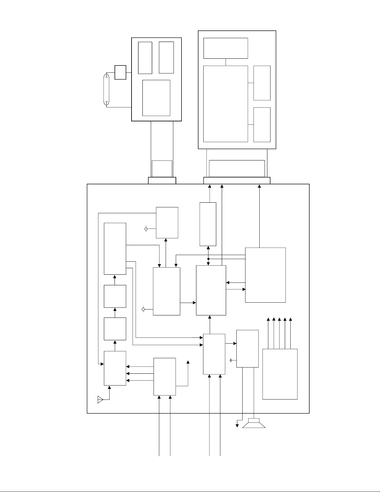
VCOM AMP
(NJM3414AVP)
L-PCB
BT
LAMP
SUB-PCB
VCC2
BS
BV
VCC7
BATTERY 1.5V
x
4 AFT
AC ADAPTOR 6V
VCC1-1 EXT-R
EXT-G
LCM
COD30T3015LN
EXTERNAL VIDEO
VIDEO2
VCOM
EXTERNAL AUDIO
R,G,B
VCC1-1
AUDIO2
Vcc7(30V)
Vcc6(18.5V)
Vcc5(12V)
Vcc2(4.8V)
Vee1(-10.5V)
CN920
CN700
CSYNC
HDB
FRP
CLR,SRT1,MCLK
BU
VIDEO1
AUDIO1
ANT
TUNER
(TEPE5-01)
LCD
384*243
INVERTER
TRANS
(C-8126)
CH
UPKEY
CH
DOWNKEY
SOURCE
DRIVER
SOURCE
DRIVER
GATE DRIVER
EAR
PHONE
SP
VCC2-4
DOWNUPVCC1-1
GND
VCC6
VCC5-1
VCC2-5
GND
VEE1
MCLK
CLROESRTL
SRTR
RESET
GSRT
GPCK
GRES
HCNT
MCLK
CLROESRTL
SRTL
SRTR
RESET
GSRT
GPCK
GRES
HCNT
POWER SW
BAND SW
AV JACK
AUDIO AMP
(NJM2070M)
DC/DC
CONVERTER
TRANS
TFT
CONTROLER
(CM7017L3)
TFT
CHROMA
(IR3Y18A)
TUNING
CONTROLER
(SED3950F)
PRE
AMP
SAW
FILTER
VIF/SIF
(M51348FP)
TUNING
BT AMP
(BA10358)
BT
BLOCK DIAGRAM
— 2 —
Page 5
ADJUSTMENT
1. Vcc2 adjustment, Vcc7, Vcc6, Vcc5, Vee1 voltage check
2. LLD coil adjustment
3. Free running frequency adjustment
4. VOM AC and VCOM DC coarse adjustment
5. Contrast, Bright adjustment
6. COLOR adjustment
7. BCC coil adjustment
8. VCOM DC adjustment
Preparations
1. For the above 1 - 7 adjustments, connect JACK to the ground GND(OV).
Adjustment And Test Point Locations
CP238
CP750
T200
VR730
T300
CP344
VR300
CP711
CP324
CP308
CP705
VR301
VR303
CP725
VR710
CP108
CP109
CP106
CP107
CP101
VR100
CP105
Top View Bottom View
— 3 —
Page 6
Adjustment procedures (EV-660C/I/N)
1. VCC2 adjustment, VCC7, VCC6, VCC5, VEE1 voltage check
• Condition
(1) Signal
No signal
(2) Other conditions
Power supply: Vcc1-1 = 5.00 ± 0.05 [V]
• Adjustment
Apply 5.00 ± 0.05 [V] on Vcc1-1.
Adjust VR100 so that Vcc2 (CP108) voltage becomes 4.80 ± 0.02 [V].
• Checking
VCC7 (CP105) = 27.1 ~ 33.4 [V]
VCC6 (CP106) = 18.0 ~ 20.0 [V]
VCC5 (CP107) = 11.0 ~ 13.0 [V]
VEE1 (CP109) = –12.0 ~ –10.0 [V]
• Block diagram
L-PCB
VCC1-1
Stabilizer
VCC7
VCC6
VCC5
VCC2
VEE1
V
Digital
Voltmeter
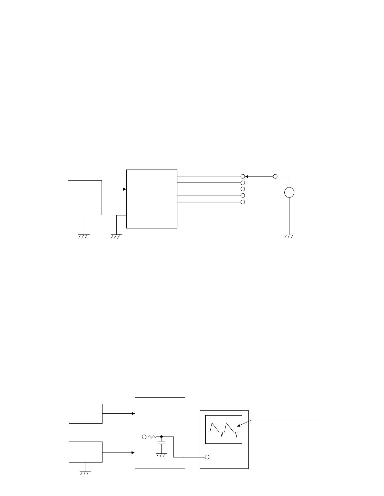
2. LLD coil adjustment
• Conditions
(1) Signals
Broadcasting system: B/G
Color system: PAL color bar
(2) Signal level
Input electric field: 46 ± 3 dBµ (IF AGC full gain), P/S = 10 dB
(3) Other conditions
CCIR IF (Input electric field: terminated with 75 Ω resistance)
As to VIDEO signal, use signal source equivalent to TG7.
Power supply: Vcc1-1 = 5.00 ± 0.05 [V]
• Adjustment
Monitor video detection signal (CP238) via a low-pass filter of 100 kHz cutoff frequency and adjust LLD coil
T200 so that its DC level is minimum (waveform’s amplitude is maximum).
• Confirmation
There should be no waveform distortion (erroneous synchronization, etc.), under sensitivity (video detector
output level is abnormally small, etc.).
• Block diagram
Signal
generator
Stabilizer
IF signal
VCC1-1
L-PCB
Detector OUT
Low-Pass Filter
Adjust to minimize the DC level.
DC IN
Oscilloscope
— 4 —
Page 7
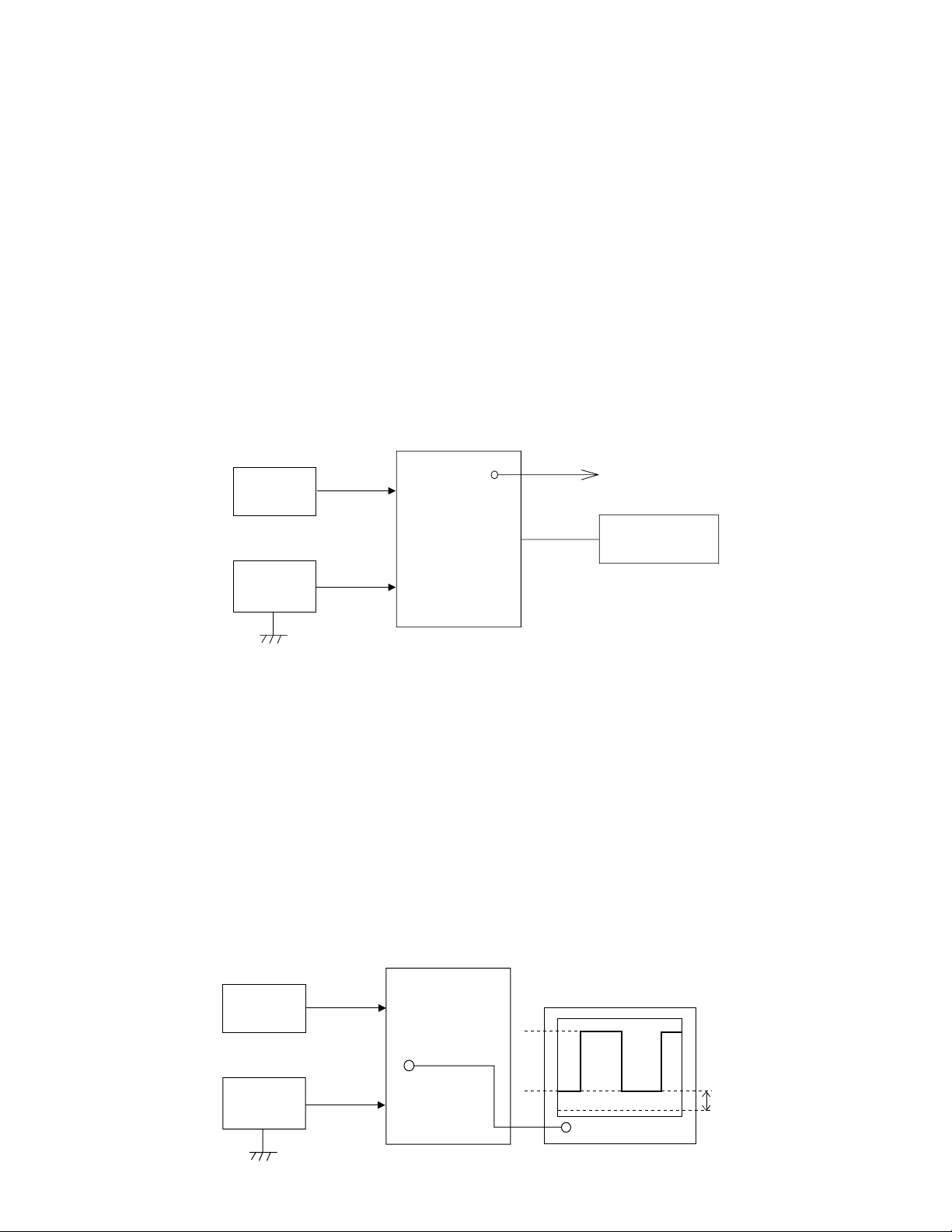
3. Free running frequency adjustment
• Conditions
(1) Signal
No signal (PAL standard signal should be applied only at synchronous check)
(2) Signal level
Input electric field only at synchronous check: 70 ± 3 dBµ (terminated with 75Ω resistance),
P/S = 10 dB
(3) Other conditions
CCIR IF input only at synchronous check (input electric field with 75 Ω termination).
Connect SYF terminal (CP725) and GND.
Power supply: Vcc1-1 = 5.00 ± 0.05 [V]
Room temperature: 20 ± 10 [°C]
• Adjustment
Monitoring HDB (CP705) with a frequency counter, adjust VR710 so that the frequency is 15.625 ± 0.1 [kHz].
• Caution
(1) Disconnect the wire between SYF terminal. Applying IF signal make sure that synchronization is normal
on the display.
• Block diagram
Signal
generator
IF signal
SYF
GND
HDB
Frequency
Counter
Stabilizer
L-PCB
VCC1-1
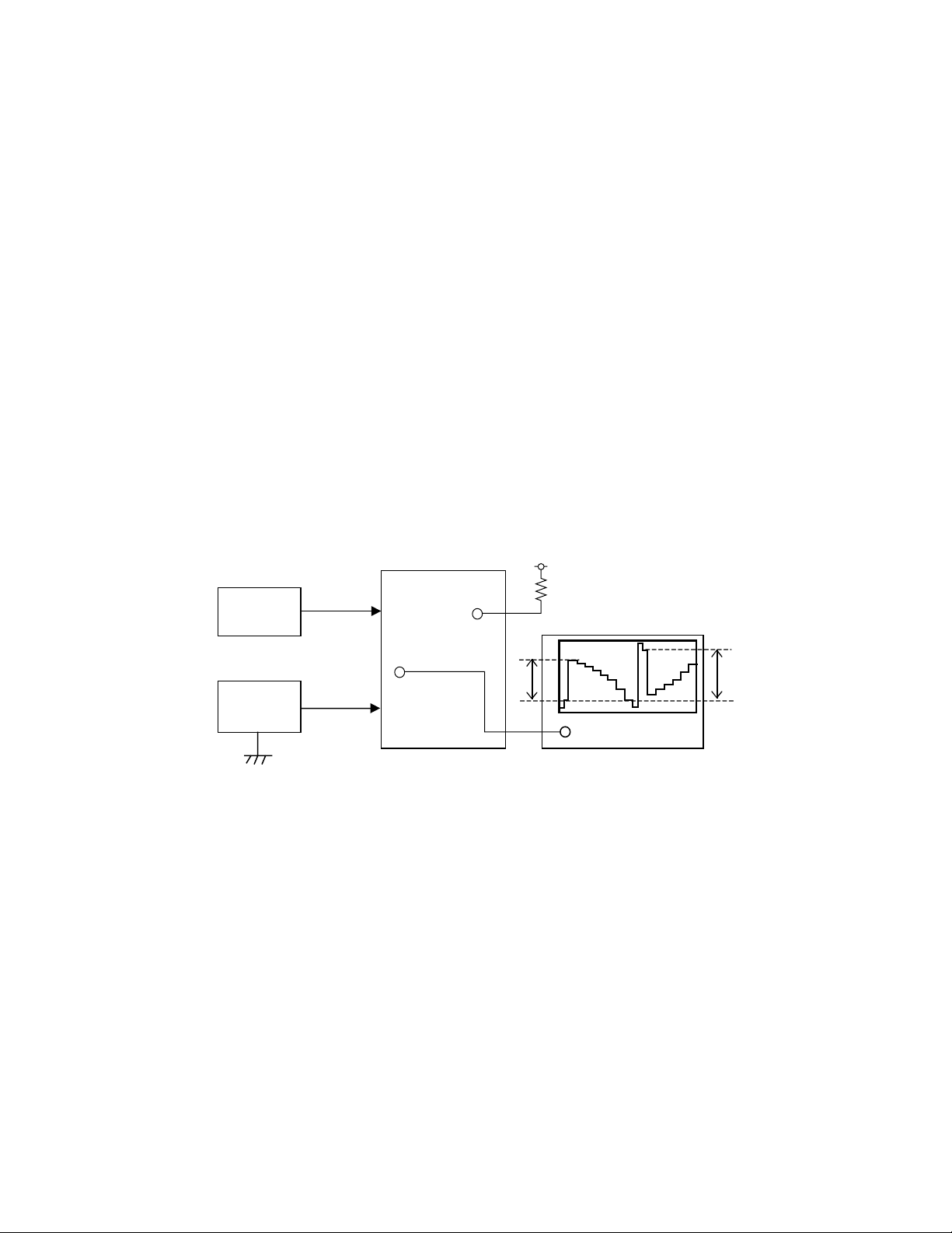
4. VCOM AC and VCOM DC coarse adjustment
• Conditions
(1) Signals
Broadcasting system: B/G
Color system: PAL color bar
(2) Signal level
Input electric field: 70 ± 3dBµ (terminated with 75Ω resistance), P/S = 10 dB
(3) Others
CCIR IF input (input electric field should be terminated with 75Ω resistance)
Use VIDEO signal equivalent to TG7.
Power supply should be Vcc1-1 = 5.00 ± 0.05V.
• Adjustment
(1) Confirm that the amplitude of VCOM output (CP750) is 6.0 ± 0.5 [V].
(2) Adjust VR730 so that Low level voltage of VCOM output (CP750) is 2.4 ± 0.2 [V].
• Block diagram
L-PCB
Signal
generator
IF signal
Stabilizer
VCC1-1
CP750
— 5 —
6.0 V
Oscilloscope
2.4 V
GND
Page 8
5. Contrast, Bright adjustment
• Conditions
(1) Signals
Broadcasting system: B/G
Color system: PAL color bar
(2) Signal level
Input electric field: 70 ± 3 dBµ (terminated with 75Ω resistance), P/S = 10 dB
(3) Others
CCIR IF input (input electric field should be terminated with 75Ω resistance)
As to VIDEO signal, use signal source equivalent to TG7.
Supplying power should be VCC1-1 = 5.00 ± 0.05 V
• Adjustment
(1) Apply VCC2-3 (CP344) voltage on KILLER terminal (CP308) via 22 kΩ resistance.
(2) Triggering FRP signal (CP71 1), observe VB waveform (CP324) and adjust BRIGHT VR so that pedes-
tal-pedestal voltage becomes 5.0 ± 0.1[V].
(3) Adjust VR303 so that VB (CP324) waveform's pedestal - white peak voltage is 3.5 ± 0.1[V].
• Caution
(1) Make sure that waveforms are not distorted.
(2) After the adjustment, disconnect VCC2-3 voltage from the killer terminal.
(Reference: Use white 75% for PAL color bar.)
(3) Do not move BRIGHT VR until TINT and COLOR adjustments are completed.
• Block diagram
Signal
generator
Stabilizer
IF signal
VCC1-1
B output
L-PCB
CP308
3.5 – 0.1 V
VCC2-3
22 KΩ
5.0 – 0.1 V
Oscilloscope
— 6 —
Page 9

6. COLOR adjustment
• Condition
(1) Signal
Broadcasting system: B/G
Color system: PAL color bar
(2) Signal level
Input electric field: 70 ± 3 dBµ (75Ω termination), P/S = 10 dB
(3) Other conditions
CCIR IF input (input electric field should be terminated with 75Ω resistance).
Use VIDEO signal equivalent to TG7.
Apply voltage of Vcc1-1 = 5.00 ± 0.05 [V]
• Adjustment
Adjust VR300 so that 4th pulse of VB waveform's (CP324) pedestal-peak amplitude is 3.5 Vp-p.
• Caution
(1) Perform after Contrast adjustment.
(2) VB waveform's pedestal-pedestal voltage should be fixed on 5.0 ± 0.1 [V].
• Block diagram
L-PCB
B output
3.5 Vp-p
Oscilloscope
Signal
generator
Stabilizer
IF signal
VCC1-1
7. BCC coil adjustment
• Condition
(1) Signal
Broadcasting system: B/G
Color system: PAL color bar
(2) Signal level
Input electric field: 70 ± 3 dBµ (75Ω termination), P/S = 10 dB
(3) Other conditions
CCIR IF input (input electric field should be terminated with 75Ω resistance).
Use VIDEO signal equivalent to TG7.
Apply voltage of Vcc1-1 = 5.00 ± 0.05 [V]
• Adjustment
Adjust BCC coil (T300) so that center 2 pulses of VB waveform (CP324) become level (3.5 ± 0.1 [V].)
• Caution
(1) Perform after COLOR adjustment.
(2) VB waveform's pedestal-pedestal voltage should be fixed on 5.0 ± 0.1 [V].
• Block diagram
L-PCB
B output
Oscilloscope
— 7 —
Signal
generator
Stabilizer
IF signal
VCC1-1
Page 10
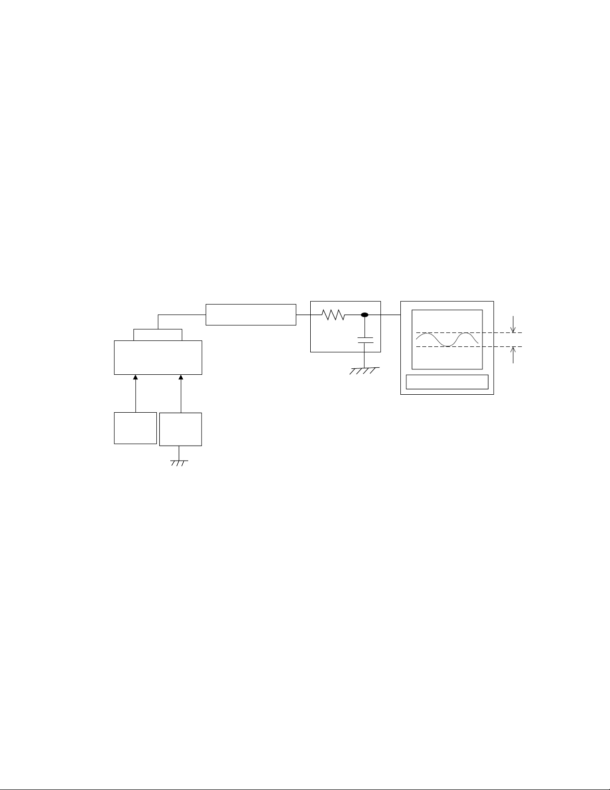
8. VCOM DC adjustment
• Conditions
(1) Signals
Broadcasting system: B/G
Color system: PAL
(2) Signal: Provide any PAL signal from AV Jack.
(3) Others
Power supply should be Vcc1-1 = 5.00 ± 0.05V.
• Adjustment
Monitoring Photo sensor AMP output with an oscilloscope via 50Hz band-pass filter, adjust VCOM DC VR
(VR730) so that 50Hz ripple component is minimum.
• Caution
Perform this adjustment when you replaced the display module.
Use specified jig to replace photoelectric parts
• Block diagram
Photo diode
EV-660C/I/N
AV JACK
Signal
generator
S1133
VCC1-1
Stabilizer
B.P.F.
Photosensor amp.
C2719
Oscilloscope
— 8 —
Page 11

Adjustment procedures (EV-660D)
1. VCC2 adjustment, VCC7, VCC6, VCC5, VEE1 voltage check
• Condition
(1) Signal
No signal
(2) Other conditions
Power supply: Vcc1-1 = 5.00 ± 0.05 [V]
• Adjustment
Apply 5.00 ± 0.05 [V] on Vcc1-1.
Adjust VR100 so that Vcc2 (CP108) voltage becomes 4.80 ± 0.02 [V].
• Checking
VCC7 (CP105) = 27.1 ~ 33.4 [V]
VCC6 (CP106) = 18.0 ~ 20.0 [V]
VCC5 (CP107) = 11.0 ~ 13.0 [V]
VEE1 (CP109) = –12.0 ~ –10.0 [V]
• Block diagram
L-PCB
VCC1-1
Stabilizer
VCC7
VCC6
VCC5
VCC2
VEE1
V
Digital
Voltmeter
2. LLD coil adjustment
• Conditions
(1) Signals
Broadcasting system: I
Color system: PAL color bar
(2) Signal level
Input electric field: 46 ± 3 dBµ (IF AGC full gain), P/S = 7 dB
(3) Other conditions
UK IF (Input electric field: terminated with 75 Ω resistance)
As to VIDEO signal, use signal source equivalent to TG7.
Power supply: Vcc1-1 = 5.00 ± 0.05 [V]
• Adjustment
Monitor video detection signal (CP238) via a low-pass filter of 100 kHz cutoff frequency and adjust LLD coil
T200 so that its DC level is minimum (waveform’s amplitude is maximum).
• Confirmation
There should be no waveform distortion (erroneous synchronization, etc.), under sensitivity (video detector
output level is abnormally small, etc.).
• Block diagram
Signal
generator
Stabilizer
IF signal
VCC1-1
L-PCB
Detector OUT
Low-Pass Filter
Adjust to minimize the DC level.
DC IN
Oscilloscope
— 9 —
Page 12

3. Free running frequency adjustment
• Conditions
(1) Signal
No signal (PAL standard signal should be applied only at synchronous check)
(2) Signal level
Input electric field only at synchronous check: 70 ± 3 dBµ (terminated with 75Ω resistance),
P/S = 7 dB
(3) Other conditions
UK IF input only at synchronous check (input electric field with 75 Ω termination).
Connect SYF terminal (CP725) and GND.
Power supply: Vcc1-1 = 5.00 ± 0.05 [V]
Room temperature: 20 ± 10 [°C]
• Adjustment
Monitoring HDB (CP705) with a frequency counter, adjust VR710 so that the frequency is 15.625 ± 0.1 [kHz].
• Caution
(1) Disconnect the wire between SYF terminal. Applying IF signal make sure that synchronization is normal
on the display.
• Block diagram
Signal
generator
IF signal
SYF
GND
HDB
Frequency
Counter
Stabilizer
L-PCB
VCC1-1
4. VCOM AC and VCOM DC coarse adjustment
• Conditions
(1) Signals
Broadcasting system: I
Color system: PAL color bar
(2) Signal level
Input electric field: 70 ± 3dBµ (terminated with 75Ω resistance), P/S = 7 dB
(3) Others
UK IF input (input electric field should be terminated with 75Ω resistance)
Use VIDEO signal equivalent to TG7.
Power supply should be Vcc1-1 = 5.00 ± 0.05V.
• Adjustment
(1) Confirm that the amplitude of VCOM output (CP750) is 6.0 ± 0.3 [V].
(2) Adjust VR730 so that Low level voltage of VCOM output (CP750) is 2.4 ± 0.2 [V].
• Block diagram
L-PCB
Signal
generator
IF signal
Stabilizer
VCC1-1
CP750
— 10 —
6.0 V
Oscilloscope
2.4 V
GND
Page 13

5. Contrast, Bright adjustment
• Conditions
(1) Signals
Broadcasting system: I
Color system: PAL color bar
(2) Signal level
Input electric field: 70 ± 3 dBµ (terminated with 75Ω resistance), P/S = 7 dB
(3) Others
UK IF input (input electric field should be terminated with 75Ω resistance)
As to VIDEO signal, use signal source equivalent to TG7.
Supplying power should be VCC1-1 = 5.00 ± 0.05 V
• Adjustment
(1) Apply VCC2-3 (CP344) voltage on KILLER terminal (CP308) via 22 kΩ resistance.
(2) Triggering FRP signal (CP71 1), observe VB waveform (CP324) and adjust BRIGHT VR so that pedes-
tal-pedestal voltage becomes 5.0 ± 0.1[V].
(3) Adjust VR303 so that VB (CP324) waveform's pedestal - white peak voltage is 3.5 ± 0.1[V].
• Caution
(1) Make sure that waveforms are not distorted.
(2) After the adjustment, disconnect VCC2-3 voltage from the killer terminal.
(Reference: Use white 75% for PAL color bar.)
(3) Do not move BRIGHT VR until TINT and COLOR adjustments are completed.
• Block diagram
Signal
generator
Stabilizer
IF signal
VCC1-1
B output
L-PCB
CP308
3.5 ± 0.1 V
VCC2-3
22 KΩ
5.0 ± 0.1 V
Oscilloscope
— 11 —
Page 14

6. COLOR adjustment
• Condition
(1) Signal
Broadcasting system: I
Color system: PAL color bar
(2) Signal level
Input electric field: 70 ± 3 dBµ (75Ω termination), P/S = 7 dB
(3) Other conditions
UK IF input (input electric field should be terminated with 75Ω resistance).
Use VIDEO signal equivalent to TG7.
Apply voltage of Vcc1-1 = 5.00 ± 0.05 [V]
• Adjustment
Adjust VR300 so that 4th pulse of VB waveform's (CP324) pedestal-peak amplitude is 3.5 Vp-p.
• Caution
(1) Perform after Contrast adjustment.
(2) VB waveform's pedestal-pedestal voltage should be fixed on 5.0 ± 0.1 [V].
• Block diagram
L-PCB
B output
Signal
generator
IF signal
3.5 Vp-p
Oscilloscope
Stabilizer
VCC1-1
7. BCC coil adjustment
• Condition
(1) Signal
Broadcasting system: I
Color system: PAL color bar
(2) Signal level
Input electric field: 70 ± 3 dBµ (75Ω termination), P/S = 7 dB
(3) Other conditions
UK IF input (input electric field should be terminated with 75Ω resistance).
Use VIDEO signal equivalent to TG7.
Apply voltage of Vcc1-1 = 5.00 ± 0.05 [V]
• Adjustment
Adjust BCC coil (T300) so that center 2 pulses of VB waveform (CP324) become level (3.5 ± 0.1 [V].)
• Caution
(1) Perform after COLOR adjustment.
(2) VB waveform's pedestal-pedestal voltage should be fixed on 5.0 ± 0.1 [V].
• Block diagram
L-PCB
Signal
generator
IF signal
Stabilizer
B output
VCC1-1
Oscilloscope
— 12 —
Page 15

8. VCOM DC adjustment
• Conditions
(1) Signals
Broadcasting system: I
Color system: PAL
(2) Signal: Provide any PAL signal from AV Jack.
(3) Others
Power supply should be Vcc1-1 = 5.00 ± 0.05V.
• Adjustment
Monitoring Photo sensor AMP output with an oscilloscope via 50Hz band-pass filter, adjust VCOM DC VR
(VR730) so that 50Hz ripple component is minimum.
• Caution
Perform this adjustment when you replaced the display module.
Use specified jig to replace photoelectric parts
• Block diagram
Photo diode
AV JACK
Signal
generator
S1133
EV-660D
Stabilizer
VCC1-1
B.P.F.
Photosensor amp.
C2719
Oscilloscope
— 13 —
Page 16

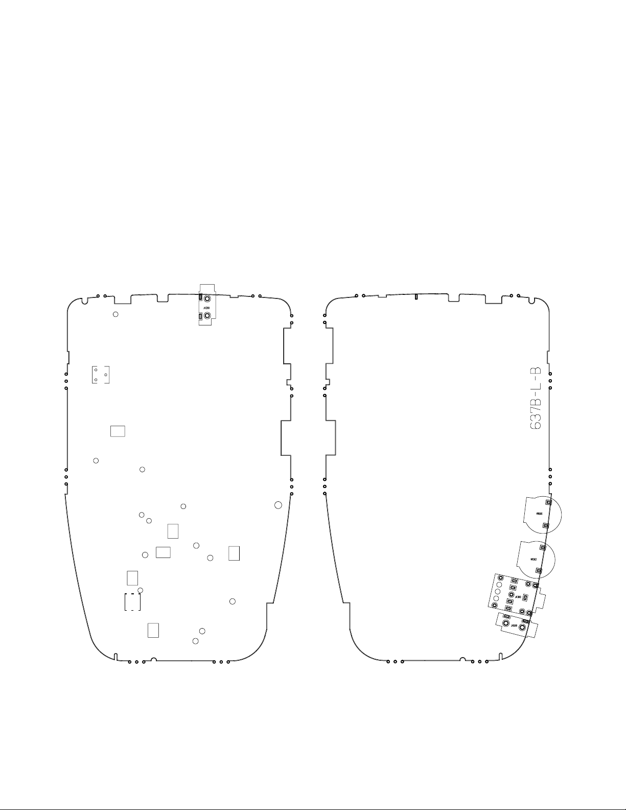
TOP VIEWS
Linear
PRINTED CIRCUIT BOARDS
Back Light
— 14 —
Page 17

BOTTOM VIEWS
Linear
Back Light
— 15 —
Page 18
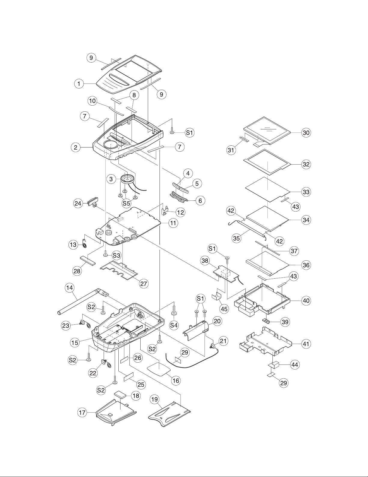
EXPLODED VIEW
9
1
14
13
2
24
28
10
8
7
3
S5
S3
27
9
S1 30
7
4
5
6
12
11
S1
38
31
42
35
32
33
43
34
42
37
36
43
23
15
S2
17
S2
22
S2
18
26
25
S2
19
S4
16
— 16 —
29
S1
20
45
21
40
39
41
44
29
Page 19

PARTS PRICE LIST
EV-660CIND
N Item Code No. Parts Name Specification Model Q
Price Code
N 1
6614 3770 Upper panel CIM-K637 K140608-3 EV-660C
1 AR X
1 1001 9341
Upper panel DAM-K637 K140608-5 EV-660D
1 AR X
N 1
6614 3760 Upper panel NCM-K637 K140608-2 EV-660I/N
1 AW X
2
6614 3080 Upper case BXM-K637 K140607-1 EV-660C/N
1 AT X
2 1001 9343
Upper case DAM-K637 K140607-3 EV-660D
1 AP X
N 2
6614 3780 Upper case IAM-K637 K140607-2 EV-660I
1 AP X
3
3831 1102
Speaker 28-8FB-04 Common 1 AK B
4 6614 3060 Tuning key A-K637 K441741-1 Common 1 AE X
5 6614 3070 Tuning key B-K637 K441742-1 Common 1 AE X
6 6614 3050 Tuning button A-K637 K341588-1 Common 1 AA X
7
6600 4290 Adhesive tape C-K51 K451-16
Common 2 AA X
N 8
6614 3090 Adhesive tape A-K637 K441818-1
Common 2 AA X
N 9
6614 3110 Adhesive tape B-K637 K441819-1
Common 2 AA X
N 10 1001 9345
Adhesive tape C-K637 K441915-1
Common 1 AA X
N 11 6614 3715 Linear PCB K241251*1 EV-660C/I/N 1 DD A
N 11 1001 9366 Linear PCB K241309*1 EV-660D 1 DZ A
N 12 6614 3160 Antenna terminal A-K637 K341655-1 Common 1 AB X
N 13 6614 3170 Battery spring B-K637 K441740-1 Common 1 AB X
14 3851 1848
Rod antenna
YC-KX-541-M2 Common
1 AP B
15 6614 3620 Lower case BXM-K637 K140609-1
EV-660C/N/D
1 AH X
N 15
6614 3750 Lower case IAM-K637 K140609-2 EV-660I
1 AI X
N 16
6614 3720 Rating plate CIM-K637 K341673-2 EV-660C
1 AB X
N 16 1001 1338
Rating plate DAM-K637 K341673-6 EV-660D
1 AA X
N 16
6614 3740 Rating plate IAM-K637 K341673-4 EV-660I
1 AB X
N
16 6614 3730 Rating plate NCM-K637 K341673-3 EV-660N
1 AB X
17 6614 3010 Battery coverBXM-K637 K140613-1 Common 1 AA C
N 18
6614 3030 Cushion B-K637 K441851-1 Common
1 AA C
19 6614 3020 Stand BXM-K637 K140614-1 Common 1 AA C
20 6614 3120 Battery holder A-K637 K241201-1 Common 1 AA X
N 21 6614 3610 Battery spring A-K637 K441739-1 Common 1 AB X
22 6020 7658 Battery spring B1 G513 P408A-1 Common
1 AB X
23 6020 7666 Battery spring B2 G513 P409A-1 Common
1 AA X
24 6614 2990 Switch K637 K341589-1 Common 1 AA X
25
6608 0920
Battery label B-K533 K411564-2 Common 1 AA X
26 6612 4711 Battery label B-K613 K412056A-2 Common 1 AA X
N
27 6614 3040 Sealed plate B-K637 K341701-1 Common
1 AE X
N 28
6614 2980 Cushion A-K637 K441850-1 Common
1 AA X
29 6601 1700 Insulation A-K60 K4117-3 Common
2 AA X
30 2725 1383 LCD COD30T3015LN Common 1 DP A
31 6600 3050 Insulation plate K-K52 K452-14 Common
1 AA X
N
32 6614 3680 Spacer K441780-1 Common
1 AB X
33 6614 3180
Light diffuser sheet A-
K441779-1 Common
1 AW X
N
34 6614 3660 Leadin light plate A-K637 K340708-2 Common
1 AS X
35 3851 2121 Fluorescent lamp CAS-24JES3.0-1 Common 1 AY A
36 6614 3650 Reflector sheet A-K637 K441781-1 Common
1 AD X
37
6611 5860 Adhesive tape D-K613 K412009-3 Common
1 AA X
N 38
6614 2969
BL PCB K341685*1 Common 1 BS B
N 39 6614 2970 BL PCB K341685*2 Common 1 AP B
N
40 6614 3630 Reflector case A-K637 K140615-1 Common
1 AG X
Note : Q - Quantity per unit
R - Rank
- 17 -
R
Page 20

Item Code No. Parts Name Specification Applicable Q R
41
6614 3640 Sealed case K637 K241193-1 Common
1 AD X
42
6611 5050 Adhesive tape A-K617 K440939-1 Common
2 AA X
43
6605 9650 Adhesive tape C-K604 K410642-3 Common
2 AA X
N
44 6614 3670 Sealed plate A-K637 K441788-1 Common
1 AA X
45 6607 0690 Insulation plate D-K508 K410441-3 Common
1 AA X
S1 5860 0420
Screw
BT3 1.7X4 NI Common
4 AA X
S2 5860 1449
Screw
BT3 1.7X8 BK Common
4 AA X
S3 6604 3110
Screw
K41310-1 Common
1 AA X
S4 6609 1290 Screw A-K610 K412031-1 Common
1 AA X
S5 6630 7430 Screw A-K618 K440305-1 Common
3 AA X
Note : Q - Quantity per unit
R - Rank
- 18 -
Page 21

LINEAR (EV-660C/I/N)
Speaker
Earphone
Jack
SCHEMATIC DIAGRAMS
Audio Amplifier Circuit
Chroma Circuit
External
Antenna
Jack
IF Detection Circuit
Tunner
Power Switch
Power Supply Circuit
AC Jack
25.0 ~ 30.0 V
18.0 ~ 20.0 V
11.0 ~ 13.0 V
± 0.02 V
4.8
–12.0 ~ –10.0 V
Display Controller Circuit
— 19 —
Page 22

LINEAR (EV-660D)
Speaker
Earphone
Jack
Audio Amplifier Circuit
Chroma Circuit
External
Antenna
Jack
IF Detection Circuit
Tunner
Power Switch
Power Supply Circuit
AC Jack
25.0 ~ 30.0 V
18.0 ~ 20.0 V
11.0 ~ 13.0 V
± 0.02 V
4.8
–12.0 ~ –10.0 V
Display Controller Circuit
— 20 —
Page 23

BACK LIGHT
— 21 —
Page 24

Ver.1 : PARTS LIST (P.17) was changed.
CASIO TECHNO CO.,LTD.
Overseas Service Division
Nishi-Shinjuku Kimuraya Bldg. 1F
5-25, Nishi-Shinjuku 7-Chome
Shinjuku-ku, Tokyo 160-0023, Japan
 Loading...