

Page 1

EV-510C(PAL B / G,H)
INDEX
EV-510D(PAL I)
EV-510I (PAL B / G)
EV-510N(PAL B / G,H)
FEB. 1997
(without price)
UHF
VHF
13
30
1
2
3
< TUNNING >
EV-510
40
50
62
4681012
CH
CH
R
Page 2

CONTENTS
SPECIFICATIONS ......................................................................................... 1
BLOCK DIAGRAM ........................................................................................ 2
PRINTED CIRCUIT BOARDS ....................................................................... 3
EXPLODED VIEW ......................................................................................... 5
PARTS LIST .................................................................................................. 6
SCHEMATIC DIAGRAMS ............................................................................. 9
WAVEFORMS.............................................................................................. 12
Page 3
SPECIFICATIONS
Item Specification
1. Power voltage DC 6.0 V
2. Power consumption Approx. 2.3 W
3. Current consumption Approx. 383 mA
Batteries : 3 AA size batteries
4. Power supply Car adaptor : CA-K65
AC adaptor : AD-K65
Earphone jack : 3.5ø mini
5. Connection terminals External power jack : 6.0 V DC IN
External antenna jack : 3.5ø mini
Audio / Video jack : 3.5ø
6. Screen size 2.5 inches
7. No. of Picture element 61,380 (220 × 279) dots
8. Dimensions 75 (W) × 26.7 (D) × 120.8 (H) mm
9. Weight 195 g excepting batteries
AC adaptor : AD-K65, 64
10. Options Car adaptor : CA-K65
RF connector : CF-13
Antenna matching device : AS-35S
Model Color System TV System Channel
EV-510C/N PAL B/G, H CCIR VHF: 2 ~ 12 ch UHF: 21 ~ 69 ch
EV-510D PAL –/I UK — UHF: 21 ~ 68 ch
EV-510I PAL B/G ITALY VHF: A ~ H2 ch UHF: 21 ~ 69 ch
— 1 —
Page 4
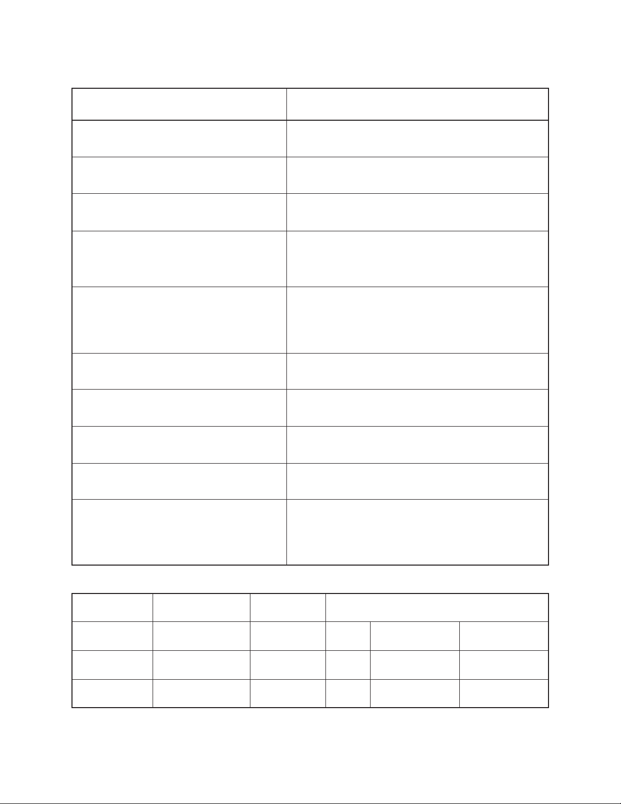
Antenna
BLOCK DIAGRAM
Power
Supply
1 TU200 2 Q200
IF Amp.Tuner
7
IC270
Tuning
Voltage
Generator
VCC2 (4.5 ± 0.02 V)
VCC7 (25.9 ~ 31.3 V)
VCC6 (10.8 ~ 12.0 V)
VEE1 (–8.5 ~ –7.5 V)
VEE2 (–19.8 ~ –17.2 V)
3 IC200
Video
Sound Det.
FM
AFT Circuit
AGC Circuit
5
6
IC300
Chroma
Circuit
IC700
Display
Control
Auto-Tuning
Control
Det
4 IC600 Speaker
VR600
Audio
Amp.
Volume
Control
LCD
1 — Color tuner: TU200 TEPE5-01 (EV-510C/I/N) TEPB5-05 (EV-510D)
Selects a desired radio wave and changes it to the video IF signal.
2 — Video IF amp.: Q200 2SC4238
Amplifies the video IF signal output from tuner TU200 by 10 times (20 dB).
3 — Video det./Sound det./FM det./AFT/AGC: IC200 M51348FP
Eliminates the carrier wave in the video IF signal, and picks up the video signal and the sound IF signal.
Also, the sound signal is picked up from the sound IF signal by FM detection.
4 — Audio amp.: IC600 NJM2070M
Sound amplification.
5 — Chroma circuit: IC300 IR3P96-1
Generates the tricolor (red, green, and blue) from the video signal.
6 — Display control/Auto-tuning control: IC700 MSM6770CGS
Controls the display.
7 — Tuning voltage generator: IC270 BA10358F
Generates the tuning voltage with the tuning pulse output from 6.
— 2 —
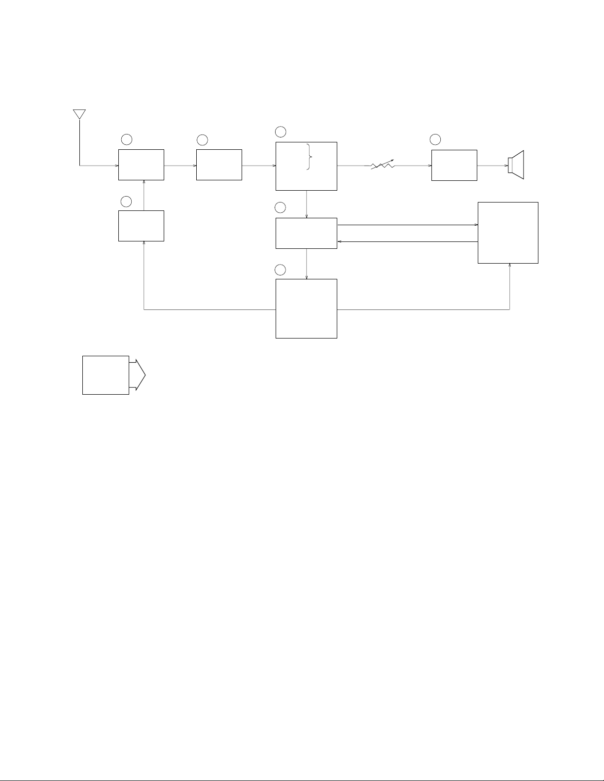
Page 5
,
,
TOP VIEWS
PRINTED CIRCUIT BOARDS
Linear
JK200
C225
GND GND
+
C202
+
TU200
+
L101
+
+
C118
C746R780
C120
C112
VR100
SW100
R105
TM100
+
C100
C145
T100
C114
IC700
615C-L
R736
D180
JK100
FU100
C353
C352
C306
+
C305
C334
R737
C333
+
L301
H300
C300
R750
R751
C725
L310
+
+
R761
C781
R312
C355
C374
C312
R302
C315
+
C110
+
C116
+
1
C752
C375
C220
L102
R715
Q760
R716
R707
R705
R701
HP900
+
+
C215
F200
+
C205
R212R209R222
C245
GND
T201 T200
+
+
C710
R710
R711
Q710
R706
C606
R703
+
C600
C603C311
+
C376C381
C380
C301
+
C207
C259
R758
Q750
R759
+
C236R223
C208
+
R224
R227
R230
C257
+
C210
+
,
,
JK250
JK600
R229
F203 F202 F201
CN700
VR600
VR304
BL
615BL
R720
CN702
L950
Q951
R950
— 3 —
Q950
C925
T950
CN950
C927
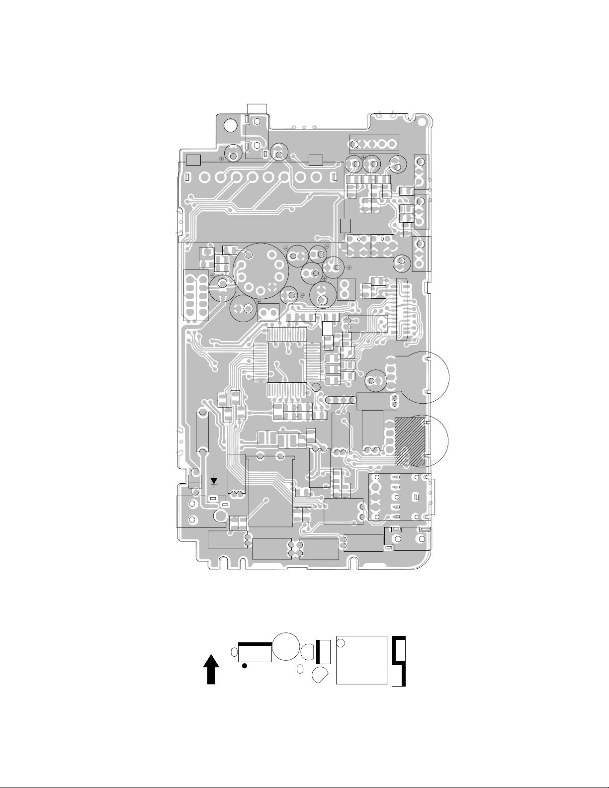
Page 6

BOTTOM VIEWS
Linear
CP790
CP706
CP791
CP235
R225
R226C250L202R247
R793
CP321
CP320
HP601
C242
C249
CP240
R770
R645
HP600
R208
IC200
CP245
R246
C791
CP794
C787
CP795
R600C630
R615
R610
R352
CP224
C246C236
C243
R239
C261
C790
R771
C792
CP701
Q600
C631
R606
R607
IC600
R611
R353
R281R280
Q204
CP280
C264
R228
C795C796
CP703
CP704
CP322
R330R331
R241
C263
CP792
CP707
CP705
CP323
R334R335
R300
C240
R205
L200
C239
R204
Q200
R201
1
HP200
R211 C233
VR200
C262
R150
CP115
CP114
CP101
CP718
CP756
C750
C788
R704
C787
R757L756 R756
CP726
CP717
R351
R350
VR303
IC300
R332R333
1
VR300
R301
C330
C350
C351
R360
C357
R282
R203
R202
C237
CP221
CP210
C232C231 C200
CP211
R277
CP110
D150
D152
CP111
CP724
C751
CP793
VR740
C786
C773
R760
C373
R324
C372
CP312
CP206
R207
Q272
R325
C371
R304
C354
CP209
R276
Q270
R275
R115C140
R749
IC701
C774
CP750
R322
C310
C365
C361
R303
C356
CP208
C271
CP100
R160
D158
C146
D156
D154
CP113
C150
CP780
C770
R315
R323C364
R314
R316
C335C336
R363
R311
C362
L300
R305
CP303
R270
IC270
L740
CP741
C772
C337
R310
CP207
C137
R108
D110
R739
R740R741
CP301
R313
C363
C360
C234
R271
R110
Q111
D100
CP310
CP311
CP330
T300
R210
R272
C270
R113
Q110
C771
C185
HP110
C181
HP100
CP200CP204
C230
Q101
C105
R107
CP185
R175
R170
BL
CP990
CP900
SW701
— 4 —
CP903
CP902
SW700
Page 7

EXPLODED VIEW
1
3
2
23
5
9
10
6
4
8
11
7
24
24
20
19
21
22
14
23
12
13-1
25
15
16
23
13
26
24
18
17
— 5 —
Page 8

PARTS LIST
LINEAR PCB
Item Code No. Parts Name Specification Applicable Q R
Diodes
D100 2390 1183 Chip diode MA142WK-(TX) Common
D110 2315 0158 Chip zener diode MA3051-L(TX) Common
D150 2390 1183 Chip diode MA142WK-(TX) Common
D152 2390 1183 Chip diode MA142WK-(TX) Common
D154 2390 1183 Chip diode MA142WK-(TX) Common
D156 2390 1183 Chip diode MA142WK-(TX) Common
D158 2390 1470 Chip diode MA143A-(TX) Common
D180 2390 1190 Chip diode ERA15-01Y Common
Fuse
FU100 3632 0469 Fuse PI-251001(F10) Common
ICs
IC200 2114 1827 Linear IC M51348FP-T1 Common
IC270 2116 0119 OP AMP BA10358F-T1 Common
IC300 2114 3479 Linear IC IR3P96-1 Common
IC600 2114 2464 Linear IC NJM2070M-T1 Common
IC700 2015 0147 LSI MSM6770CGS-2K-6004 Common
IC701 2114 3458 IC S-81230SG-QB-T1 Common
Jacks
JK100 3501 8281 Jack HEC0811-010010 Common
JK200 3501 5439 Jack HSJ1456-01-210 Common
JK250 3501 3773 Jack HSJ6063-01-410 Common
JK600 3501 5439 Jack HSJ1456-01-210 Common
Transistors
Q101 2253 0133 Chip transistor 2SD1819A-R(TX) Common
Q110 2253 0133 Chip transistor 2SD1819A-R(TX) Common
Q111 2253 0308 Chip transistor 2SD1119-R(TX) Common
Q200 2252 0707 Chip transistor 2SC4238-(TX) Common
Q204 2210 8026 Chip transistor 2SB709A-R(TX) Common
Q270 2259 1435 Digital transistor DTC144EUWT106 Common
Q600 2259 1645 Digital transistor DTA144EUWT106 Common
Q750 2251 0189 Chip transistor 2SB1218A-R(TX) Common
Q760 2251 0189 Chip transistor 2SB1218A-R(TX) Common
Switches
SW100 3412 0938 Slide switch ESD-11V231 EV-510C/I/N
SW100 3412 1134 Slide switch ESD-11V221 EV-510D
Converter
T100 3065 0518 DC-DC converter LC12U-35 Common
Tuners
TU200 1013 5315 Tuner TEPE5-01 EV-510C/I/N
TU200 1014 8570 Tuner TEPB5-05 EV-510D
Variable resistors
VR304 2765 1708 Volume XV081PV1NB10K3017 Common
VR600 2765 1708 Volume XV081PV1NB10K3017 Common
C
1
C
1
C
1
C
1
C
1
C
1
C
1
C
1
B
1
C
1
C
1
C
1
C
1
C
1
C
1
C
1
C
1
C
1
C
1
B
1
B
1
B
1
C
1
C
1
C
1
C
1
C
1
C
1
C
1
C
1
B
1
C
1
C
1
C
1
C
1
Notes: Q – Quantity used per unit
R – Rank
— 6 —
Page 9

BL PCB
Item Code No. Parts Name Specification Applicable Q R
Transistors
Q950 2253 0287 Chip transistor 2SD965-R Common
Q951 2253 0287 Chip transistor 2SD965-R Common
Switches
SW700 3412 1029 Switch SKHHAL Common
SW701 3412 1029 Switch SKHHAL Common
Transformer
T950 3012 1239 Inverter trans NT-06 Common
B
2
B
2
2C
2C
B
1
Notes: Q – Quantity used per unit
R – Rank
— 7 —
Page 10

COMPONENT
Item Code No. Parts Name Specification Applicable Q R
1 6611 8750 Display plate CIM-K619 K440980-2 EV-510C
1 6611 8790 Display plate DDM-K619 K440980-3 EV-510D
1 6611 8820 Display plate NBM-K619 K440980-6 EV-510I/N
2 6609 9080 Adhesive tape A-K615 K440178-1 Common
3 6611 5090 Upper cover AAM-K617 K240130-3 EV-510C/D/N
3 6611 9020 Upper cover I-K619 K240130-5 EV-510I
4 6609 9031 Upper case B-K615 K140049A-1 EV-510C/I/N
4 6610 2661 Upper case D-K615 K140049A-3 EV-510D
5 6020 7658 Battery spring B1 G513 P408A-1 Common
6 6020 7666 Battery spring B2 G513 P409A-1 Common
7 6609 9070 Battery spring A-K615 K440159-1 Common
8 6609 9060 Battery spring B-K615 K440243-1 Common
9 6611 8840 Battery cover AAM-K617 K240129-4 EV-510C/D/I/N
10 6609 9050 Battery blind plate A-K615 K440179-1 Common
11 6611 4975 BL PCB unit K440948*1 Common
12 6609 9220 Switch knob A-K615 K340117-1 Common
13 6611 8717 Linear PCB ass'y K340740*2 EV-510C/I/N
13 6611 8718 Linear PCB ass'y K340740*3 EV-510D
13-1 6609 9090 Flat cable A-K615 K340176-1 Common
14 3851 1470 Rod antenna VR70100GA Common
15 3831 0987 Speaker 2083G Common
16 6609 8970 Lower case B-K615 K140050-1 EV-510C/D/N
16 6610 2130 Lower case I-K615 K140050-3 EV-510I
17 6611 8770 Rating plate DDM-K619 K440981-3 EV-510D
18 6608 8420 Stand A-K331 K310518-1 Common
19 6611 5150 Cushion A-K615 K440931-1 Common
20 6611 5160 Cushion B-K615 K440931-2 Common
21 2725 1326 Display unit COD25T2015PB Common
22 6611 4978 BL unit K340703*1 Common
23 5112 0868 Screw BT3 1.7X5 Bk Common
24 5860 0420 Screw BT3 1.7X4 Ni Common
25 6609 1290 Screw A-K610 K412031-1 Common
26 6609 9680 Jack cover A-K611 K340237-1 EV-510D/I/N
C
1
C
1
C
1
X
1
X
1
X
1
X
1
X
1
X
1
X
1
X
1
X
1
X
1
X
1
C
1
X
1
B
1
B
1
C
1
B
1
C
1
X
1
X
1
X
1
C
1
X
2
X
2
B
1
A
1
C
4
C
6
C
1
X
1
Notes: Q – Quantity used per unit
R – Rank
— 8 —
Page 11

LINEAR (EV-510C/I/N)
Antenna
SCHEMATIC DIAGRAMS
Earphone Jack
8 9
3 4
External
Antenna
Jack
Tuner
IF Pad
Power Switch
Speaker
1
Power Supply Circuit
Tuning Voltage Generator Circuit
Audio Amplifier Circuit
IF Detection Circuit
5
17
To Back
Light
Audio/Video
Jack
DC In
Chroma Circuit
7
Display Controller
6
16
15
2
14
13
12
11
10
Circuit
To LCD
— 9 —
Page 12

LINEAR (EV -510D)
Antenna
Earphone Jack
8 9
3 4
External
Antenna
Jack
Tuner
IF Pad
Power Switch
Speaker
1
Power Supply Circuit
Tuning Voltage Generator Circuit
Audio Amplifier Circuit
IF Detection Circuit
5
17
To Back
Light
Audio/Video
Jack
DC In
Chroma Circuit
7
Display Controller
6
16
15
2
14
13
12
11
10
Circuit
To LCD
— 10 —
Page 13

BL
— 11 —
Page 14

120 mV
125 µs
5 V
G IC300 pin 30
4.5 V
64 µs
F IC700 pin 7
WAVEFORMS
64 µs
1 Q200 collector
64 µs
4 IC200 pin 18
2 IC300 pin 20
1.0 V
5 IC300 pins 32, 34, 36
4.4 V
64 µs
64 µs
4.0 V
3 IC200 pins 19, 20
4.5 V
6 IC300 pin 21
1.5 V
80.0 mV
64 µs
4.4 V
64 µs
10 V
7 IC300 pin 39
0 IC700 pin 1
C IC700 pin 4
125 µs
64 µs
64 µs
8 Q111 base
2.8 V
A IC700 pin 2
2.8 V
3 µs
D IC700 pin 5
12 µs
125 µs
9 Q111 collector
2.8 V
B IC700 pin 3
4.5 V
E IC700 pin 6
12 µs
2.8 V
64 µs
4.5 V
64 µs
— 12 —
Page 15

MA0400471A
8-11-10, Nishi-Shinjuku
Shinjuku-ku, Tokyo 160, Japan
Telephone: 03-3347-4926
 Loading...