

Page 1
(with price)
INDEX
EV-2500C/I/N (KX-618C/I/N)
JUL. 1995
R
Page 2

CONTENTS
SPECIFICATIONS ......................................................................................... 2
BLOCK DIAGRAM ........................................................................................ 3
CIRCUIT DESCRIPTION ............................................................................... 4
DISASSEMBLY ............................................................................................. 5
DIAL STRINGING DIAGRAM........................................................................ 6
ADJUSTMENT............................................................................................... 7
TROUBLESHOOTING................................................................................. 12
PRINTED CIRCUIT BOARDS ..................................................................... 13
EXPLODED VIEW ....................................................................................... 15
ELECTRICAL PARTS LIST......................................................................... 16
MECHANICAL PARTS LIST ....................................................................... 23
IC AND TRANSISTOR LEAD IDENTIFICATION ........................................ 25
SCHEMATIC DIAGRAMS ........................................................................... 27
WAVEFORMS.............................................................................................. 29
— 1 —
Page 3
SPECIFICATIONS
Item Specification
1. Reception channels TV— EV-2500C/N: VHF: 2 ~ 12 ch UHF: 21 ~ 69 ch
EV-2500I : VHF: A ~ H2 ch UHF: 21 ~ 69 ch
RADIO— FM: 88~108 MHz AM: 530~1710 KHz
2. Power voltage DC 6.0 V
3. Power consumption Approx. 3.5 W
4. Current consumption Approx. 580 mA
5. Battery life (with alkaline batteries) Approx. 11 hours
Batteries : 3 D size batteries
6. Power supply Car adaptor : CA-K65
AC adaptor : AD-K65, 64
Earphone jack : 3.5ø mini
7. Connection terminals External power jack : 6.0 V DC IN
External antennea jack : 3.5ø mini
Audio / Video jack : 3.5ø
8. Screen size 2.5 inches
9. No. of picture element 61,380 (220 × 279) dots
10. Dimensions 115 (W) × 61.7 (D) × 112 (H) mm
4 1/2 (W) × 2 2/5 (D) × 4 2/5 (H)
11. Weight 360 g excepting batteries
12.7 oz excepting batteries
AC adaptor : AD-K65,64
12. Options Car adaptor : CA-K65
RF connector : CF-13
Antenna matching device : AS-35S
— 2 —
Page 4
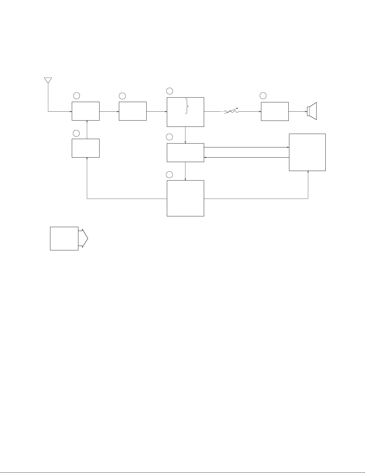
TV
Antenna
BLOCK DIAGRAM
Power
Supply
1 TU200 2 Q200
IF Amp.Tuner
7
IC270
Tuning
Voltage
Generator
VCC1 (4.5 ± 0.05 V)
VCC2 (4.5 ± 0.05 V)
VCC7 (25.9 ~ 31.3 V)
VCC6 (10.0 ~ 12.0 V)
VEE1 (–8.0 ~ –7.0 V)
VEE2 (–18.4 ~ –16.0 V)
3 IC200
Video
Sound Det.
FM
AFT Circuit
AGC Circuit
5
6
Det
IC300
Chroma
Circuit
IC700
Display
Control
Auto-Tuning
Control
4 IC600 Speaker
VR600
Audio
Amp.
Volume
Control
LCD
1 — Color tuner: TU200 TEPU5-02
Selects a desired radio wave and changes it to the video IF signal.
2 — Video IF amp.: Q200 2SC4238
Amplifies the video IF signal output from tuner TU200 by 10 times (20 dB).
3 — Video det./Sound det./FM det./AFT/AGC: IC200 M51348FP
Eliminates the carrier wave in the video IF signal, and picks up the video signal and the sound IF signal.
Also, the sound signal is picked up from the sound IF signal by FM detection.
4 — Audio amp.: IC600 NJM2070M
Sound amplification.
5 — Chroma circuit: IC300 IR3P90Y
Generates the tricolor (red, green, and blue) from the video signal.
6 — Display control/Auto-tuning control: IC700 MSM6770GS
Controls the display.
7 — Tuning voltage generator: IC270 BA10358F
Generates the tuning voltage with the tuning pulse output from 6.
— 3 —
Page 5
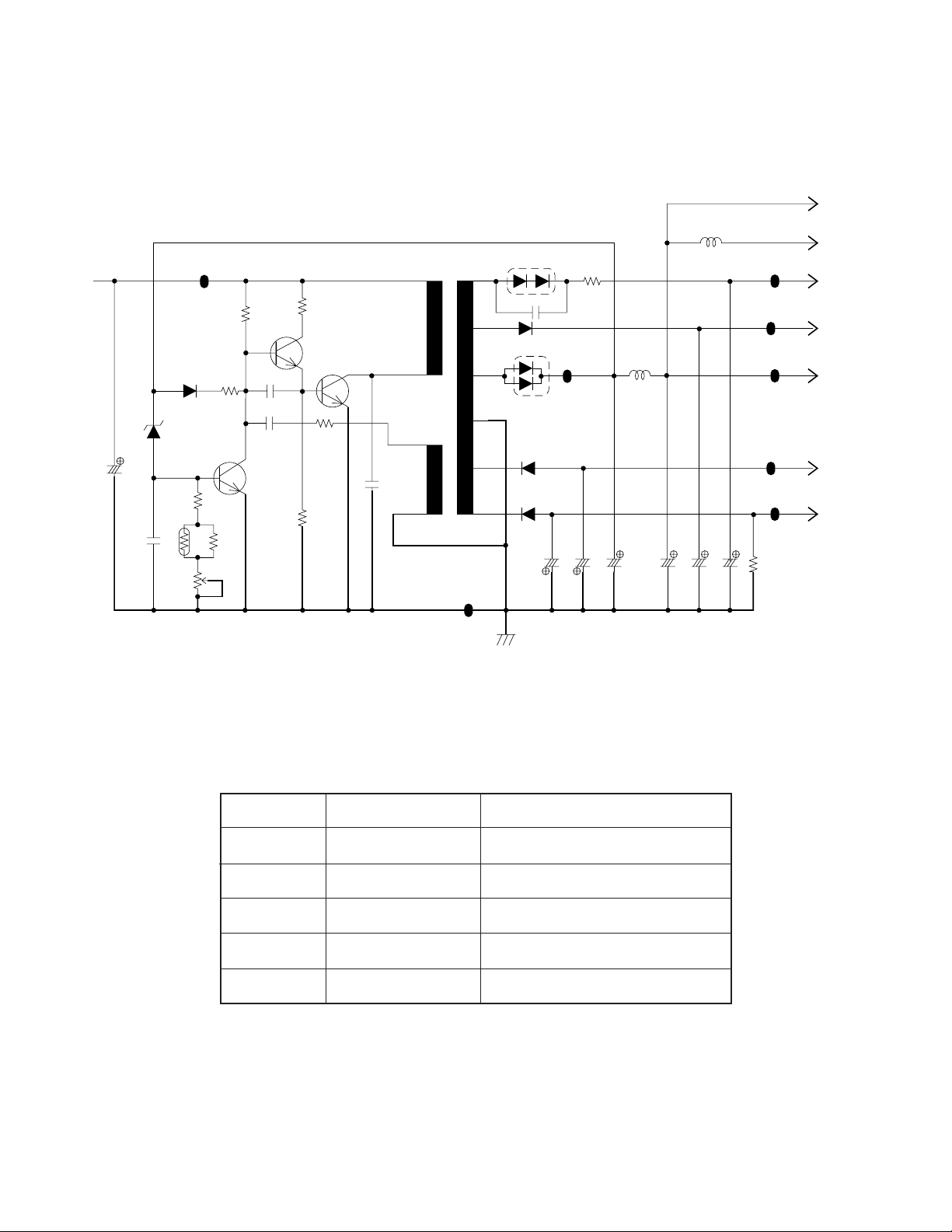
POWER SUPPLY
CIRCUIT DESCRIPTION
VCC2-3 (4.5 V)
6.3 V 220C100
CP105
D100
R107
MA141K 33K B6800p
D110
2.2
C105
Q101
2SD1819A-R
MA3051-L
0R00
R100
BH102K
TM100
2K
VR100
270K
R108
Q110 2SD1819A-R
C137
C140
CH470p
3.3K
R105
270
R110
Q111
2SD1119-R
R115
100
2.2KR113
C145
2
1
9
B1500p
6
T100
LC12U-35
CP106
GND
Figure 1
D158 MA143A
3
C146
4
D156 MA141K
1
5
2
D154 MA142WK
6
D152
MA142WK
7
D150
MA142WK
8
OPEN
3
CP112
C110 25 V 10
R160
68
10SL6R8M
C112
C114 6SL 15M
L101
100u
L102
100u
C116 6.3 V 100
C118 16 V 22
VCC2-2 (4.5 V)
VCC7 (25.9 ~ 31.3 V)
CP110
VCC6 (10.0 ~ 12.0 V)
CP111
VCC2-1 (4.5 V)
CP113
VEE1 (-8.0 ~ -7.0 V)
CP114
VEE2 (-18.4 ~ -16.0 V)
CP115
C120 35 V 22
R161 33K
The power supply consists of a DC-DC converter and the associated circuit and supplies the voltages as shown
in Table 1.
Name Voltage Function
VCC2-1 4.50 ± 0.02 V Main voltage
VCC7 25.9 ~ 31.3 V Tuning voltage
VCC6 10.0 ~ 12.0 V Display voltage
VEE1 –8.0 ~ –7.0 V Display voltage
VEE2 –18.4 ~ –16.0 V Display voltage
Table 1
— 4 —
Page 6
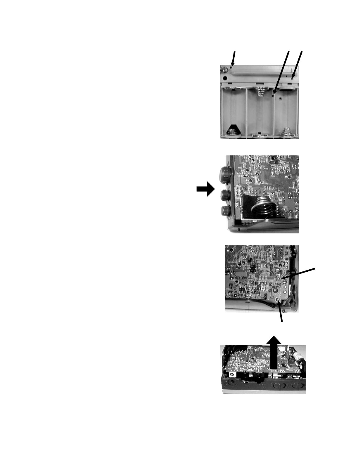
DISASSEMBLY
1. Remove the battery case.
2. Remove the three screws and the lower case.
3. Remove the three knobs.
4. Remove the screw and resolder the two wires for the speaker.
5. Remove the PCB ass'y.
— 5 —
Page 7
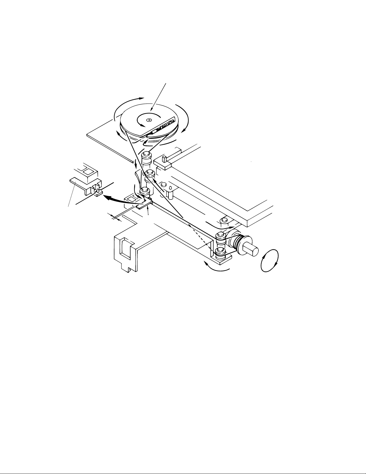
Sliding pointer
9
1
0.8 mm
DIAL STRINGING DIAGRAM
Turn the pulley counterclockwise.
2
0
3
8
4
A
5
7
6
Wrap around 4 times.
— 6 —
Page 8
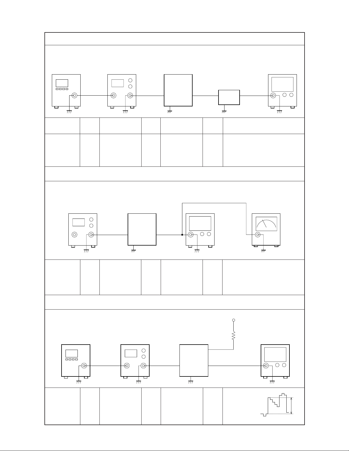
ADJUSTMENT
TV
Items to Be Adjusted
Item Measuring Instrument
VCC2-1 voltage setting Voltmeter
Video detection coil adjustment TV signal generator, pattern generator, oscilloscope,
low-pass filter
AFT coil adjustment Sweep generator, oscilloscope, voltmeter
Contrast adjustment TV signal generator, pattern generator, oscilloscope
Tint adjustment TV signal generator, pattern generator, oscilloscope
AGC adjustment TV signal generator, pattern generator, IF levelmeter
Vcom adjustment Photo diode, photo sensor amp., bandpass filter, oscilloscope
Free-Running frequency adjustment
Frequency counter
RADIO
When the radio is defect, replace the radio PCB unit.
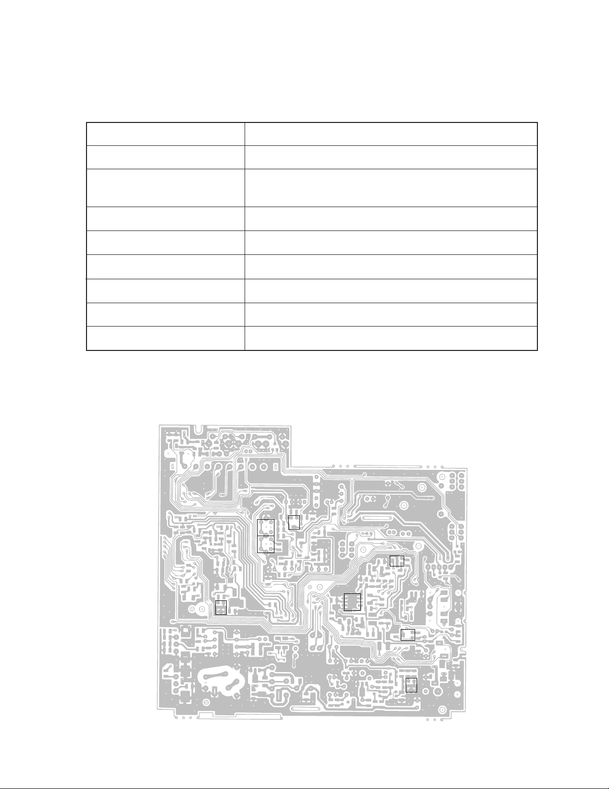
Adjustment and Test Point Locations
T201
T200
VR740
VR200
VR303
T300
Top View
— 7 —
VR300
VR100
Page 9
IF Pad
TP2 (CP201)
TP7 (CP208)
TP8 (CP334)
TP5 (CP339)
TP6 (CP322)
Bottom View
Equipment Connection / Adjustment Procedure
VCC2-1 Voltage Setting
TP4 (CP217)
TP3 (CP218)
TP1 (CP113)
EV-2500
16-169
set
Output
TP1
Input Input Input Output Output
Connection Point Signal Connection Point
Adjust Result
VR100
Voltmeter
— 8 —
Voltmeter
TP1
Adjust to obtain a 4.50 ± 0.02 V
reading on the voltmeter.
Page 10
* Desolder the IF pad to open.
Pattern
generator
Signal
generator
Video Detection Coil Adjustment
EV-2500
set
Input
TP2
Output
TP3
Oscilloscope
Low-pass
filter
Input Input Input Output Output
Connection Point Signal Connection Point
Pattern
generator
Signal
generator
TP2 T200 TP3
Color bar
38.9 MHz
(EV-200C,I,N)
39.5 MHz
(EV-200D)
45 ± 3 dBµ
Adjust Result
Low-pass filter
Oscilloscope
AFT Coil Adjustment
* Desolder the IF pad to open.
EV-2500
set
Oscilloscope
Output
TP4
Voltmeter
Oscilloscope
Sweep
generator
Sweep
generator
Input
TP2
38.9 ± 5 MHz
(sweep) marker:
38.9 MHz (EV-200C,I,N)
TP2 T201 TP4
39.5 ± 5 MHz
(sweep) marker:
39.5 MHz (EV-200D)
70 ± 3 dBµ
Adjust to obtain the minimum
DC level.
Voltmeter
Adjust to obtain a 1.4 ± 0.2 V
reading on the voltmeter.
Confirm that the marker is at
the middle of the S-curve on
the oscilloscope.
* Desolder the IF pad to open.
Pattern
generator
Pattern
generator
Signal
generator
TP2 VR300 TP5
Color bar
38.9 MHz
(EV-200C,I,N)
39.5 MHz
(EV-200D)
70 ± 3 dBµ
Signal
generator
Contrast Adjustment
EV-2500
set
Input
TP2
Oscilloscope
— 9 —
TP1
10 kohm
CP312 (KILLER)
Output
TP5(VC)
Adjust so
that the step
form wave
becomes 2.8
± 0.1 Vp-p.
Oscilloscope
2.8 ± 0.1 V
P.P
Page 11

* Desolder the IF pad to open.
BCC Adjustment
Pattern
generator
Signal
generator
EV-2500
set
Input
TP2
Input Input Input Output Output
Connection Point Signal Connection Point
Adjust Result
TP5(VC)
Color bar
Pattern
generator
Signal
generator
TP2 T300 Oscilloscope TP5
38.9 MHz
(EV-200C,I,N)
39.5 MHz
(EV-200D)
70 ± 3 dBµ
AGC Adjustment
* Short the IF pad.
Pattern
generator
Signal
generator
EV-2500
set
Oscilloscope
Output
Adjust T300 so that the
difference
between pulses
A and B is less
than 0.1 V.
IF levelmeter
Pulse BPulse A
Pattern
generator
TV signal
generator
Input
TP7
Color bar
TP7 VR200 IF levelmeter TP2
65 ± 5 dBµ
Vcom Adjustment
EV-2500
set
Oscilloscope
Output
TP8
VR303 Oscilloscope TP8
Output
TP2
Adjust to obtain a 84 ± 2 dBµ
reading on the IF levelmeter.
Adjust VR303 so that the
high level of the square wave
is at -0.5
± 0.25 V.
5.0 ± 0.5 V
-0.5 ± 0.25 V
— 10 —
Page 12

Vcom Adjustment
* Place a photo diode on the middle of the display plate.
EV-2500
set
Photo
diode
Photo sensor amp.
Bandpass
filter
ON
H
M
OFF
L
AV-C1
Audio/Video jack
Input Input Input Output Output
Connection Point Signal Connection Point
Adjust Result
Photo sensor
VR303
amp.
Bandpass filter
Oscilloscope
Free-Running Frequency Adjustment
EV-2500
set
Frequency
counter
Oscilloscope
Adjust to obtain the minimum
ripple.
Output
TP6
VR740 TP6
Frequency
counter
Adjust to obtain a reading of
15.625 ± 0.1 kHz.
— 11 —
Page 13

TV
TROUBLESHOOTING
Symptom Cause Solution
No power supply Defective power switch (SW100). Replace.
No picture and
no sound
Picture OK but
no sound
Defective DC-DC converter (T100). Replace.
Defective tuner (TU200). Replace.
Defective Q200. Replace.
Defective IC200. Replace.
Defective IC300. Replace.
Defective IC270. Replace.
Defective IC700. Replace.
Defective F201. Replace.
Defective IC200. Replace.
Defective IC600. Replace.
Defective phone jack (JK600). Replace.
No reception of
VHF or UHF
Defective tuner (TU200). Replace.
Defective IC270. Replace.
Defective power switch (SW100). Replace.
RADIO
When the radio is defect, replace the radio PCB unit.
— 12 —
Page 14

TV
C535
R500
C536
L500
C531
D500
R501
C532
R537
PRINTED CIRCUIT BOARDS
C202
D520
C630
R600
C631
R601
R323
C791
R770
R704
C710
C793
R706
R776
R775
R325
L790
C792
R611
R602
C750
Q710
R610
C744
L760
R717
L761
C635
TU200
R739
R715
R716
Q760
C771
C746
C751
C773
C770
R749
C772
VR740
T201
R741
R731
R740
L750
T200
L740
618C - L - A
R606
R607
Q951
Q950
R240
R274
R951
R223
R236
C259
R238
R239
R227
C512
R229
C257
C511
Q515
C207
R214
VR200
R950
C205
R210
R222
R230
R224
C930
C247
L203
C246
C250
R226
R225
F200
C265
C208
R246
R243
D156
R160
F203
C201
R242
D158
C146
T300
D154
C319
R312
R309
C310
C324
R316
C306
R305
Q111
C510
Q516
R318
C327
R315
C314
L303
L300
L302
Q110
C145
R110
R317
R310
C304
R115
R108
VR303
C326
R319
R302
D100
C140
Q101
C137
R320
R300
D110
R107
H300
R322
R327
R326
R328
R330
VR300
R100
C105
R321
C340
TM100
VR100
R301
C330
R105
Q510
R392
C181
FU100
Q390
O
Q513
R515
R535
R391
R390
R645
B
Top view
— 13 —
Page 15

TV
SW100
CP102
SW102
1
JK300
C390
JK600
JK100
C185
CN510
C308
C305
C329
D180
CP100
C339
C341
R329
C342
R331
C100
C331
C332
C336
CP307
CP310
CP734
CP300
C110
CP105
CP112
CP106
HP100
C335
1
C300
C334
CP337
CP334
CP339
IC300
C301
C302
D150
R161
C325
CP335
C328
C303
C307
CP114
D152
R113
R512R513
Q511
R514
CP327
C322
C320
C321
R303
C112
T100
Q514
Q512
C312
R306
C318
R311
C317
C315
C309
C114
GY
L202
R516
SW101
CP322
C313
L301
R307
L101
R247
C311
C116
C118
C120
R208
L201
C242
C243
C248
C249
F201
D510
D511
C240
R211
R212
CP341
L950
L200
C239
R241
C245
IC200
F202
CP213
CP115
L102
SW701
R203
R205
Q200
R204
CP223
C263
C264
C261
CP214
C210
R733
R736
CP113
CP111
C925
R201
C237
C262
CP218
R732
R734
R738
CP110
C603
SW700
R209
HP200
CP201
C233
R207
R202
C236
CP217
R727
R728
CP741
R737
C606
T950
CP202
C232
C271
R729
IC701
CP203
C270
R271
R272
IC270
IC700
CP751
CP750
C774
SW702
CP204
C200
C231
1
R275
CP726
CP724
R750
C770
R751
C725
IC600
C927
R276
R270
Q270
CP718
R760
C781
C530
Q272
CP
719
R756
R761
C600
CP900
CP209
CP210
CP206
C234
Q202
CP205
R280
L204
CP725
C760
CP703
1
L756
CN900
JK200
Q201
R758
R771
C790
CP707
R707
R705
R703
R701
C786
C787
VR600
VR304
CP208
C230
Q750
1
CP705
CP792
CP793
CP706
C788
R757
CP700
CP207
R759
CP790
CP791
CN700
CP704
CP701
CP756
CP101
Bottom view
— 14 —
Page 16

EXPLODED VIEW
25-2
47
48
25
1
19
2 3
12
11
10
3
3
48
3
47
6
8
25-5
7
7
9
7
10
28
25-6
4
5
50
6
23
24
22
26-1
51
49
21
15
49
13
26-2
50
18
33-3
51
16
17
14
56
55
49
26
25-1
25-3
48
25-4
33-2
36
37
38
33
48
34
33-1
52
43
35
48
39
28-3
28-4
34
54
28-2
32
53
42
31
28-3
41
27
28-2
40
44
28-1
28-3
30
51
26-3
26-4
26-7
26-6
26-5
46
45
— 15 —
Page 17

ELECTRICAL PARTS LIST
Linear PCB No. 1
FOB Japan
N Item Code No. Parts Name Specification Q M N.R.Yen R
Unit Price
Capacitors
C100 2800 9175 Electrolytic capacitor (V) 6.3RC2-220MS 1 20 17 C
C105 2897 2310 Chip capacitor GR42-6Y5V225Z16PT 1 20 24 C
C110 2806 9462 Electrolytic capacitor (V) 25RC2-10MS-G10 1 20 11 C
N C112 2845 5901 OS capacitor 10SL6R8M 1 10 42 C
C114 2845 5502 OS capacitor 6SL15M 1 10 43 C
C116 2805 2499 Electrolytic capacitor (V) 6.3RC2-100MS 1 20 18 C
C118 2828 5542 Electrolytic capacitor (V) 16RC2-22MS 1 20 12 C
C120 2805 2481 Electrolytic capacitor (V) 35RC2-22MS 1 20 14 C
C137 2897 0189 Chip capacitor GR40W5R682K50PT 1 20 8 C
C140 2892 0865 Chip capacitor GR40CH471J50PT 1 20 15 C
C145 2897 0252 Chip capacitor GR40W5R152K50PT 1 20 5 C
C181 2892 0040 Chip capacitor GR40Y5V104Z25PT 1 20 14 C
C185 2892 0040 Chip capacitor GR40Y5V104Z25PT 1 20 14 C
C200 2845 5488 Chip capacitor UMK316B104K-T 1 20 12 C
C201 2895 0133 Chip tantalum capacitor ECST1EY474R 1 20 27 C
C202 2800 9182 Electrolytic capacitor 6.3RC2-47MS 1 20 15 C
C205 2806 9455 Electrolytic capacitor (V) 50RC2-2R2-G9 1 20 9 C
C207 2845 1596 OS capacitor 6SC15M 1 10 37 C
C208 2806 9399 Electrolytic capacitor (V) 6.3RC2-47MS-G10 1 20 9 C
C210 2804 9234 Electrolytic capacitor (V) 16RC310 1 20 23 C
C230 2892 0059 Chip capacitor GR40Y5V103Z50PT 1 20 9 C
C232 2892 0059 Chip capacitor GR40Y5V103Z50PT 1 20 9 C
C233 2892 0059 Chip capacitor GR40Y5V103Z50PT 1 20 9 C
C234 2892 0040 Chip capacitor GR40Y5V104Z25PT 1 20 14 C
C236 2892 0059 Chip capacitor GR40Y5V103Z50PT 1 20 9 C
C237 2892 0059 Chip capacitor GR40Y5V103Z50PT 1 20 9 C
C239 2897 0245 Chip capacitor GR40CH180J50PT 1 20 6 C
C240 2892 0059 Chip capacitor GR40Y5V103Z50PT 1 20 9 C
C243 2892 0059 Chip capacitor GR40Y5V103Z50PT 1 20 9 C
C245 2892 0083 Chip capacitor GR40W5R103K50PT 1 20 14 C
C246 2892 0059 Chip capacitor GR40Y5V103Z50PT 1 20 9 C
C249 2892 0844 Chip capacitor GR42-6Y5V474Z16PT 1 20 27 C
C250 2892 0237 Chip capacitor GR40W5R222K50PT 1 20 9 C
C257 2892 0407 Chip capacitor GR40CH270J50PT 1 20 10 C
C259 2892 0083 Chip capacitor GR40W5R103K50PT 1 20 14 C
C261 2892 0890 Chip capacitor GR40PH560J50PT 1 20 13 C
C262 2892 0059 Chip capacitor GR40Y5V103Z50PT 1 20 9 C
C263 2892 0890 Chip capacitor GR40PH560J50PT 1 20 13 C
C264 2892 0474 Chip capacitor GR40CH010C50PT 1 20 10 C
C265 2892 0237 Chip capacitor GR40W5R222K50PT 1 20 9 C
C270 2892 0083 Chip capacitor GR40W5R103K50PT 1 20 14 C
C271 2897 0175 Chip capacitor GR40Y5V473Z50PT 1 20 6 C
C301 2892 0059 Chip capacitor GR40Y5V103Z50PT 1 20 9 C
C302 2892 0059 Chip capacitor GR40Y5V103Z50PT 1 20 9 C
C303 2892 0059 Chip capacitor GR40Y5V103Z50PT 1 20 9 C
C304 2897 0749 Chip capacitor GR40W5R561K50PT 1 20 5 C
C305 2800 9182 Electrolytic capacitor 6.3RC2-47MS 1 20 15 C
C307 2892 0040 Chip capacitor GR40Y5V104Z25PT 1 20 14 C
C308 2804 9064 Electrolytic capacitor (V) 16RC2-10 1 20 9 C
C310 2895 0126 Tantalum capacitor ECST1CY105R 1 20 27 C
Notes: N – New parts
M – Minimum order/supply quantity
Q – Quantity used per unit
R – Rank
— 16 —
Page 18

Linear PCB No. 2
FOB Japan
N Item Code No. Parts Name Specification Q M N.R.Yen R
Unit Price
C311 2892 0407 Chip capacitor GR40CH270J50PT 1 20 10 C
C312 2892 0237 Chip capacitor GR40W5R222K50PT 1 20 9 C
C313 2897 0217 Chip capacitor GR40W5R153K25PT 1 20 6 C
C314 2895 0126 Tantalum capacitor ECST1CY105R 1 20 27 C
C315 2892 0059 Chip capacitor GR40Y5V103Z50PT 1 20 9 C
C317 2892 0300 Chip capacitor GR40CH470J50PT 1 20 10 C
C318 2892 0105 Chip capacitor GR40CH080D50PT 1 20 10 C
C319 2897 0525 Chip capacitor GR40CH151J50PT 1 20 7 C
C320 2892 0059 Chip capacitor GR40Y5V103Z50PT 1 20 9 C
C321 2892 0059 Chip capacitor GR40Y5V103Z50PT 1 20 9 C
C322 2897 0175 Chip capacitor GR40Y5V473Z50PT 1 20 6 C
C325 2897 0350 Chip capacitor GR40CH160J50PT 1 20 6 C
C326 2892 0059 Chip capacitor GR40Y5V103Z50PT 1 20 9 C
C327 2892 0844 Chip capacitor GR42-6Y5V474Z16PT 1 20 27 C
C328 2892 0040 Chip capacitor GR40Y5V104Z25PT 1 20 14 C
N C329 2845 5901 OS capacitor 10SL6R8M 1 10 42 C
C331 2828 5516 Electrolytic capacitor (V) 16RC2-47MS 1 20 15 C
C332 2892 0059 Chip capacitor GR40Y5V103Z50PT 1 20 9 C
N C334 2806 9511 Chip capacitor 25RC2-4R7MS 1 20 9 C
C335 2892 0059 Chip capacitor GR40Y5V103Z50PT 1 20 9 C
C336 2892 0040 Chip capacitor GR40Y5V104Z25PT 1 20 14 C
C339 2892 0040 Chip capacitor GR40Y5V104Z25PT 1 20 14 C
C390 2806 9448 Electrolytic capacitor (V) 6.3RC2BP-22 1 20 20 C
C510 2806 9469 Electrolytic capacitor (V) 6.3RC2-100MS-G10 1 20 12 C
C530 2892 0059 Chip capacitor GR40Y5V103Z50PT 1 20 9 C
C531 2892 0059 Chip capacitor GR40Y5V103Z50PT 1 20 9 C
C532 2892 0059 Chip capacitor GR40Y5V103Z50PT 1 20 9 C
C535 2892 0040 Chip capacitor GR40Y5V104Z25PT 1 20 14 C
C536 2892 0040 Chip capacitor GR40Y5V104Z25PT 1 20 14 C
C600 2828 5542 Electrolytic capacitor (V) 16RC2-22MS 1 20 12 C
C603 2805 2499 Electrolytic capacitor (V) 6.3RC2-100MS 1 20 18 C
C606 2805 2499 Electrolytic capacitor (V) 6.3RC2-100MS 1 20 18 C
C630 2892 0040 Chip capacitor GR40Y5V104Z25PT 1 20 14 C
C631 2897 0504 Chip capacitor GR40W5R272K50PT 1 20 5 C
C635 2892 0016 Chip capacitor GR40W5R102K50PT 1 20 11 C
C710 2895 1897 Tantalum capacitor ECST1DY335R 1 20 22 C
C725 2897 2177 Chip capacitor TMK316B224K-T 1 20 15 C
C746 2892 0040 Chip capacitor GR40Y5V104Z25PT 1 20 14 C
C750 2892 0040 Chip capacitor GR40Y5V104Z25PT 1 20 14 C
C751 2892 0059 Chip capacitor GR40Y5V103Z50PT 1 20 9 C
C760 2892 0059 Chip capacitor GR40Y5V103Z50PT 1 20 9 C
C770 2897 2310 Chip capacitor GR42-6Y5V225Z16PT 1 20 24 C
C771 2892 0237 Chip capacitor GR40W5R222K50PT 1 20 9 C
C772 2892 0059 Chip capacitor GR40Y5V103Z50PT 1 20 9 C
C773 2897 2310 Chip capacitor GR42-6Y5V225Z16PT 1 20 24 C
C774 2892 0059 Chip capacitor GR40Y5V103Z50PT 1 20 9 C
C781 2897 0112 Chip capacitor GR40W5R562K50PT 1 20 12 C
C786 2845 5670 Chip capacitor UMK212UJ120J-T 1 20 4 C
C787 2845 5670 Chip capacitor UMK212UJ120J-T 1 20 4 C
C788 2892 0059 Chip capacitor GR40Y5V103Z50PT 1 20 9 C
C790 2892 0059 Chip capacitor GR40Y5V103Z50PT 1 20 9 C
C791 2892 0059 Chip capacitor GR40Y5V103Z50PT 1 20 9 C
C925 2825 0441 TF capacitor ECQ-V1H473JL 1 20 12 C
Notes: N – New parts
M – Minimum order/supply quantity
Q – Quantity used per unit
R – Rank
— 17 —
Page 19

Linear PCB No. 3
FOB Japan
N Item Code No. Parts Name Specification Q M N.R.Yen R
Unit Price
C927 2813 3213 Ceramic capacitor DE0405SL270J2K 1 20 13 C
Connectors
CN510 3501 9331 Connector 5512-05A 1 10 30 C
CN700 3501 8316 Connector 52559-2090 1 5 70 C
CN900 3501 1001 Connector W-P7503#11 1 20 12 C
Diodes
D100 2390 1701 Chip diode MA141K-(TX) 1 20 14 C
D110 2315 0158 Chip zener diode MA3051-L(TX) 1 10 30 C
D150 2390 1183 Chip diode MA142WK-(TX) 1 20 9 C
D152 2390 1183 Chip diode MA142WK-(TX) 1 20 9 C
D154 2390 1183 Chip diode MA142WK-(TX) 1 20 9 C
D156 2390 1701 Chip diode MA141K-(TX) 1 20 14 C
D158 2390 1470 Chip diode MA143A-(TX) 1 20 16 C
D180 2390 1190 Chip diode ERA15-01Y 1 20 9 C
D500 2390 2289 Chip diode MA558-(TX) 1 10 36 C
D510 2370 1134 LED SLB-22MG3FJ 1 20 16 C
D511 2370 1127 LED SLB-22DU3FH 1 20 16 C
D520 2390 1183 Chip diode MA142WK-(TX) 1 20 9 C
Filters
F200 3025 0189 SAW filter SAF38.9MZ60Z 1 1 150 C
F201 3025 0728 SIF filter SFSL5.5MDB12 1 10 33 C
F202 3851 1148 Ceramic discriminator CDSL5.5MC30B12 1 10 45 C
F203 3850 1372 SIF trap TPS5.5MB 1 10 30 C
Fuse
FU100 3632 0469 Fuse PI-251001(F10) 1 10 52 C
Oscillator
H300 2590 0252 Crystal oscillator NR-18C 1 1 120 C
ICs
IC200 2114 1827 Linear IC M51348FP-T1 1 1 190 B
IC270 2116 0119 OP AMP BA10358F-T1 1 10 39 C
IC300 2114 3479 Linear IC IR3P96-1 1 1 670 B
IC600 2114 3689 IC NJM2070D 1 5 60 B
IC700 2011 8337 LSI MSM6770GS-VK-675-F 1 1 300 B
IC701 2114 3458 IC S-81230SG-QB-T1 1 10 50 C
Jacks
JK100 3501 6755 Jack HEC3600-010120 1 10 42 C
JK200 3501 9324 Jack HSJ1501-010020 1 5 73 C
JK300 3501 3773 Jack HSJ6063-01-410 1 5 88 C
JK600 3501 5439 Jack HSJ1456-01-210 1 20 27 C
Inductors and Coil
L101 3840 2374 Inductor EL0405SKI-101K-2 1 10 48 C
L102 3840 2374 Inductor EL0405SKI-101K-2 1 10 48 C
L200 3013 1393 Chip inductor LK2125-R82K-TP 1 20 26 C
L202 3013 1904 Chip inductor LK2125-150K-TP 1 20 27 C
L203 2792 0110 Chip jumper ERJ-6GEY0R00V 1 20 3 C
L204 3013 0868 Chip inductor BLM21A05PT 1 20 22 C
L300 3013 1092 Chip inductor NLC322522-470K-TP 1 20 28 C
L301 3013 1204 Chip inductor MLF2012C330K-TP 1 20 29 C
L302 3013 1092 Chip inductor NLC322522-470K-TP 1 20 28 C
L303 3013 1092 Chip inductor NLC322522-470K-TP 1 20 28 C
L500 3013 1897 Chip inductor LK2125-R56K-TP 1 20 27 C
L740 3013 1043 Chip inductor NLC322522-101K-TP 1 20 28 C
L750 3013 1043 Chip inductor NLC322522-101K-TP 1 20 28 C
Notes: N – New parts
M – Minimum order/supply quantity
Q – Quantity used per unit
R – Rank
— 18 —
Page 20

Linear PCB No. 4
FOB Japan
N Item Code No. Parts Name Specification Q M N.R.Yen R
Unit Price
L756 3013 1911 Chip inductor LK2125-330K-TP 1 20 27 C
L760 3013 1848 Chip inductor BK2125HS601-T 1 20 13 C
L761 3013 1848 Chip inductor BK2125HS601-T 1 20 13 C
L790 3013 1848 Chip inductor BK2125HS601-T 1 20 13 C
L950 3013 0756 Choke coil RCH-875-101K 1 5 55 C
Lamp
N LA900
3851 1596 Fluorescent lamp HMES48B25W64C-X
1 1 280 C
Transistors
Q101 2253 0133 Chip transistor 2SD1819A-R(TX) 1 20 12 C
Q110 2253 0133 Chip transistor 2SD1819A-R(TX) 1 20 12 C
Q111 2253 0308 Chip transistor 2SD1119-R(TX) 1 10 37 C
Q200 2252 0707 Chip transistor 2SC4238-(TX) 1 20 17 C
Q201 2259 1645 Digital transistor DTA144EUWT106 1 20 10 C
Q202 2259 1645 Digital transistor DTA144EUWT106 1 20 10 C
Q270 2259 1435 Digital transistor DTC144EUWT106 1 20 9 C
Q272 2259 1834 Digital transistor DTA143TUWT106 1 20 15 C
Q390 2251 0189 Chip transistor 2SB1218A-R(TX) 1 20 10 C
Q510 2259 1645 Digital transistor DTA144EUWT106 1 20 10 C
Q511 2259 2142 Digital transistor DTA123EUWT106 1 20 10 C
Q512 2253 0133 Chip transistor 2SD1819A-R(TX) 1 20 12 C
Q513 2253 0133 Chip transistor 2SD1819A-R(TX) 1 20 12 C
Q514 2210 8026 Chip transistor 2SB709A-R(TX) 1 20 23 C
Q516 2259 1631 Digital transistor DTA114TUWT106 1 20 10 C
Q710 2253 0133 Chip transistor 2SD1819A-R(TX) 1 20 12 C
Q750 2251 0189 Chip transistor 2SB1218A-R(TX) 1 20 10 C
Q760 2251 0189 Chip transistor 2SB1218A-R(TX) 1 20 10 C
Q950 2253 0308 Chip transistor 2SD1119-R(TX) 1 10 37 C
Q951 2253 0308 Chip transistor 2SD1119-R(TX) 1 10 37 C
Resistors
R100 2792 0110 Chip jumper ERJ-6GEY0R00V 1 20 3 C
R105 2791 0742 Chip resistor ERJ-6GEYJ332V 1 20 5 C
R107 2791 0607 Chip resistor ERJ-6GEYJ333V 1 20 4 C
R108 2791 1919 Chip resistor ERJ-6GEYJ274V 1 20 3 C
R110 2791 1131 Chip resistor ERJ-6GEYJ271V 1 20 3 C
R113 2791 0720 Chip resistor ERJ-6GEYJ222V 1 20 3 C
R115 2791 0572 Chip resistor ERJ-6GEYJ101V 1 20 5 C
R160 2791 1692 Chip resistor ERJ-6GEYJ680V 1 20 3 C
R161 2791 0607 Chip resistor ERJ-6GEYJ333V 1 20 4 C
R201 2791 2117 Chip resistor ERJ-6GEYJ820V 1 20 4 C
R202 2791 2095 Chip resistor ERJ-6GEYJ682V 1 20 3 C
R203 2791 0720 Chip resistor ERJ-6GEYJ222V 1 20 3 C
R204 2791 0831 Chip resistor ERJ-6GEYJ681V 1 20 4 C
R205 2791 0688 Chip resistor ERJ-6GEYJ220V 1 20 3 C
R207 2791 1161 Chip resistor ERJ-6GEYJ151V 1 20 5 C
R208 2791 0734 Chip resistor ERJ-6GEYJ272V 1 20 3 C
R209 2791 0313 Chip resistor ERJ-6GEYJ103V 1 20 5 C
R210 2791 0305 Chip resistor ERJ-6GEYJ472V 1 20 3 C
R211 2791 0777 Chip resistor ERJ-6GEYJ104V 1 20 5 C
R212 2791 0720 Chip resistor ERJ-6GEYJ222V 1 20 3 C
R214 2791 1390 Chip resistor ERJ-6GEYJ473V 1 20 5 C
R222 2791 0696 Chip resistor ERJ-6GEYJ470V 1 20 4 C
R223 2791 2044 Chip resistor ERJ-6GEYJ124V 1 20 3 C
R224 2791 2176 Chip resistor ERJ-6GEYJ471V 1 20 3 C
Notes: N – New parts
M – Minimum order/supply quantity
Q – Quantity used per unit
R – Rank
— 19 —
Page 21

Linear PCB No. 5
FOB Japan
N Item Code No. Parts Name Specification Q M N.R.Yen R
Unit Price
R225 2791 1595 Chip resistor ERJ-6GEYJ153V 1 20 4 C
R227 2791 0313 Chip resistor ERJ-6GEYJ103V 1 20 5 C
R229 2791 2176 Chip resistor ERJ-6GEYJ471V 1 20 3 C
R230 2791 1131 Chip resistor ERJ-6GEYJ271V 1 20 3 C
R236 2797 0028 Chip resistor ERJ-6GEYJ683V 1 20 3 C
R239 2791 0580 Chip resistor ERJ-6GEYJ392V 1 20 4 C
R240 2791 0750 Chip resistor ERJ-6GEYJ223V 1 20 6 C
R241 2791 0607 Chip resistor ERJ-6GEYJ333V 1 20 4 C
R242 2791 0777 Chip resistor ERJ-6GEYJ104V 1 20 5 C
R243 2791 1131 Chip resistor ERJ-6GEYJ271V 1 20 3 C
R246 2791 1420 Chip resistor ERJ-6GEYJ331V 1 20 6 C
R247 2791 0720 Chip resistor ERJ-6GEYJ222V 1 20 3 C
R270 2791 0607 Chip resistor ERJ-6GEYJ333V 1 20 4 C
R271 2797 3983 Chip resistor RR1220P-473-D 1 20 3 C
R272 2797 3976 Chip resistor RR1220P-472-D 1 20 3 C
R274 2791 1617 Chip resistor ERJ-6GEYJ100V 1 20 3 C
R275 2791 0750 Chip resistor ERJ-6GEYJ223V 1 20 6 C
R276 2791 1390 Chip resistor ERJ-6GEYJ473V 1 20 5 C
R300 2791 2109 Chip resistor ERJ-6GEYJ393V 1 20 3 C
R301 2791 0607 Chip resistor ERJ-6GEYJ333V 1 20 4 C
R302 2797 1288 Chip resistor ERJ-6GEYK106V 1 20 3 C
R303 2797 0035 Chip resistor ERJ-6GEYJ105V 1 20 4 C
R305 2797 1197 Chip resistor ERJ-6GEYF183V 1 20 6 C
R306 2797 3549 Chip resistor ERJ-6GEYF133V 1 20 3 C
R307 2797 1778 Chip resistor ERJ-6GEYF272V 1 20 4 C
R309 2797 0035 Chip resistor ERJ-6GEYJ105V 1 20 4 C
R310 2791 1131 Chip resistor ERJ-6GEYJ271V 1 20 3 C
R311 2791 0831 Chip resistor ERJ-6GEYJ681V 1 20 4 C
R312 2791 0607 Chip resistor ERJ-6GEYJ333V 1 20 4 C
R315 2797 1267 Chip resistor ERJ-6GEYF393V 1 20 4 C
R316 2797 2114 Chip resistor ERJ-6GEYF333V 1 20 4 C
R317 2791 2079 Chip resistor ERJ-6GEYJ562V 1 20 3 C
R318 2791 0599 Chip resistor ERJ-6GEYJ822V 1 20 5 C
R319 2797 1204 Chip resistor ERJ-6GEYF203V 1 20 6 C
R320 2797 1211 Chip resistor ERJ-6GEYF223V 1 20 6 C
R321 2791 0313 Chip resistor ERJ-6GEYJ103V 1 20 5 C
R322 2791 2109 Chip resistor ERJ-6GEYJ393V 1 20 3 C
R323 2791 2109 Chip resistor ERJ-6GEYJ393V 1 20 3 C
R325 2791 0750 Chip resistor ERJ-6GEYJ223V 1 20 6 C
R326 2797 2114 Chip resistor ERJ-6GEYF333V 1 20 4 C
R327 2797 1750 Chip resistor ERJ-6GEYF273V 1 20 4 C
R328 2797 1750 Chip resistor ERJ-6GEYF273V 1 20 4 C
R329 2797 2170 Chip resistor ERJ-6GEYF363V 1 20 4 C
R330 2797 1750 Chip resistor ERJ-6GEYF273V 1 20 4 C
R331 2797 2275 Chip resistor ERJ-6GEYF243V 1 20 4 C
R390 2791 0607 Chip resistor ERJ-6GEYJ333V 1 20 4 C
R391 2791 1684 Chip resistor ERJ-6GEYJ183V 1 20 3 C
R392 2791 0704 Chip resistor ERJ-6GEYJ561V 1 20 4 C
R500 2791 0815 Chip resistor ERJ-6GEYJ102V 1 20 5 C
R501 2791 0815 Chip resistor ERJ-6GEYJ102V 1 20 5 C
R512 2791 0572 Chip resistor ERJ-6GEYJ101V 1 20 5 C
R513 2791 2052 Chip resistor ERJ-6GEYJ224V 1 20 3 C
R514 2791 0750 Chip resistor ERJ-6GEYJ223V 1 20 6 C
Notes: N – New parts
M – Minimum order/supply quantity
Q – Quantity used per unit
R – Rank
— 20 —
Page 22

Linear PCB No. 6
FOB Japan
N Item Code No. Parts Name Specification Q M N.R.Yen R
Unit Price
R515 2791 1633 Chip resistor ERJ-6GEYJ123V 1 20 3 C
R516 2791 0720 Chip resistor ERJ-6GEYJ222V 1 20 3 C
R535 2791 1595 Chip resistor ERJ-6GEYJ153V 1 20 4 C
R537 2791 1633 Chip resistor ERJ-6GEYJ123V 1 20 3 C
R600 2791 0720 Chip resistor ERJ-6GEYJ222V 1 20 3 C
R602 2792 0110 Chip jumper ERJ-6GEY0R00V 1 20 3 C
R606 2797 2345 Chip resistor ERJ-8GEYK4R7V 1 20 2 C
R607 2797 2345 Chip resistor ERJ-8GEYK4R7V 1 20 2 C
R610 2791 0696 Chip resistor ERJ-6GEYJ470V 1 20 4 C
R611 2791 2079 Chip resistor ERJ-6GEYJ562V 1 20 3 C
R645 2791 0696 Chip resistor ERJ-6GEYJ470V 1 20 4 C
R701 2791 0305 Chip resistor ERJ-6GEYJ472V 1 20 3 C
R703 2791 0305 Chip resistor ERJ-6GEYJ472V 1 20 3 C
R704 2791 0313 Chip resistor ERJ-6GEYJ103V 1 20 5 C
R705 2791 0305 Chip resistor ERJ-6GEYJ472V 1 20 3 C
R706 2791 0305 Chip resistor ERJ-6GEYJ472V 1 20 3 C
R707 2791 0305 Chip resistor ERJ-6GEYJ472V 1 20 3 C
R715 2791 0607 Chip resistor ERJ-6GEYJ333V 1 20 4 C
R716 2791 0313 Chip resistor ERJ-6GEYJ103V 1 20 5 C
R727 2791 0305 Chip resistor ERJ-6GEYJ472V 1 20 3 C
R728 2792 0110 Chip jumper ERJ-6GEY0R00V 1 20 3 C
R729 2791 0305 Chip resistor ERJ-6GEYJ472V 1 20 3 C
R731 2791 0305 Chip resistor ERJ-6GEYJ472V 1 20 3 C
R732 2791 0815 Chip resistor ERJ-6GEYJ102V 1 20 5 C
R733 2791 0815 Chip resistor ERJ-6GEYJ102V 1 20 5 C
R734 2791 0305 Chip resistor ERJ-6GEYJ472V 1 20 3 C
R736 2791 0305 Chip resistor ERJ-6GEYJ472V 1 20 3 C
R737 2791 0305 Chip resistor ERJ-6GEYJ472V 1 20 3 C
R738 2791 0305 Chip resistor ERJ-6GEYJ472V 1 20 3 C
R739 2797 1015 Chip resistor ERJ-6GEYK225V 1 20 3 C
R740 2797 3962 Chip resistor ERJ-6GEYF394V 1 20 2 C
R741 2797 1841 Chip resistor ERJ-6GEYJ512V 1 20 3 C
R749 2791 0580 Chip resistor ERJ-6GEYJ392V 1 20 4 C
R750 2791 1684 Chip resistor ERJ-6GEYJ183V 1 20 3 C
R751 2791 2095 Chip resistor ERJ-6GEYJ682V 1 20 3 C
R756 2791 0815 Chip resistor ERJ-6GEYJ102V 1 20 5 C
R757 2791 0815 Chip resistor ERJ-6GEYJ102V 1 20 5 C
R758 2797 1267 Chip resistor ERJ-6GEYF393V 1 20 4 C
R759 2797 1533 Chip resistor ERJ-6GEYF473V 1 20 5 C
R760 2791 2052 Chip resistor ERJ-6GEYJ224V 1 20 3 C
R761 2791 2052 Chip resistor ERJ-6GEYJ224V 1 20 3 C
R770 2791 0777 Chip resistor ERJ-6GEYJ104V 1 20 5 C
R771 2791 0696 Chip resistor ERJ-6GEYJ470V 1 20 4 C
R775 2791 0815 Chip resistor ERJ-6GEYJ102V 1 20 5 C
R776 2797 0252 Chip resistor ERJ-6GEYJ823V 1 20 3 C
R950 2791 0840 Chip resistor ERJ-8GEYJ821V 1 20 4 C
Speaker
SP600 3831 0784 Speaker 50-8B-02 1 1 190 C
Switches
SW100 3412 1253 Slide switch ESD-11H221 1 10 42 C
SW101 3412 1134 Slide switch ESD-11V221 1 10 45 C
SW102 3412 1253 Slide switch ESD-11H221 1 10 42 C
SW700 3412 0469 Switch SKHHLN 1 20 24 C
Notes: N – New parts
M – Minimum order/supply quantity
Q – Quantity used per unit
R – Rank
— 21 —
Page 23

Linear PCB No. 7
FOB Japan
N Item Code No. Parts Name Specification Q M N.R.Yen R
Unit Price
SW701 3412 0469 Switch SKHHLN 1 20 24 C
SW702 3412 0469 Switch SKHHLN 1 20 24 C
Coils ,Converter, and Transformer
T100 3065 0518 DC-DC converter LC12U-35 1 5 73 C
T200 3841 0700 Coil 5KAC-03A 1 5 60 C
T201 3841 0700 Coil 5KAC-03A 1 5 60 C
T300 3841 1267 Coil 5CDM-01 1 1 110 C
T950 3012 1225 Inverter trans NT-05 1 1 140 C
Thermister
TM100 2775 1085 Chip thermister 157-102-53031-TP 1 20 26 C
Tuner
TU200 1013 5315 Tuner TEPE5-01 1 1 820 C
Variable resistors
VR100 2775 1799 Chip semi-fixed resistor POZ3AN-1-202N-T00 1 20 17 C
VR200 2775 1813 Chip semi-fixed resistor POZ3AN-1-203N-T00 1 20 17 C
VR300 2775 1813 Chip semi-fixed resistor POZ3AN-1-203N-T00 1 20 17 C
VR303 2775 1820 Chip semi-fixed resistor POZ3AN-1-503N-T00 1 20 17 C
VR304 2765 1729 Volume RK09K111-10KB 1 10 42 C
VR600 2765 1736 Volume RK09K111-20KB 1 10 42 C
VR740 2775 1806 Chip semi-fixed resistor POZ3AN-1-103N-T00 1 20 17 C
Notes: N – New parts
M – Minimum order/supply quantity
Q – Quantity used per unit
R – Rank
— 22 —
Page 24

MECHANICAL PARTS LIST
N Item Code No. Parts Name Specification M N.R.Yen R
Upper case
N 1 6609 8800 Shutter A-K618 K240113-2
N 2 6610 2360 Display plate CIA-K618 K340119-3
N 2 6610 2370 Display plate IAA-K618 K340119-4
N 3 6600 9740 Adhesive tape A-K60 K4332-1
N 4 6609 8680 Display plate holder A-K618 K140051-2
N 5 6609 8690 Shutter stopper K618 K340112-1
N 6 6604 3760 Adhesive tape C-K453 K41300-1
N 7 6610 2470 Reflection tape set B-K618 K440387-1
N 8 6610 2460 Reflection tape C-K618 K440388-1
N 9 6609 8710 Tuning plate A-K618 K440226-1
10 6600 2220 Adhesive tape A-K52 K451-5
N 11 6610 0610 Radio panel BIA-K618 K340120-2
N 12 6609 8790 Upper case A-K618 K140036-2
N 12 6610 2430 Upper case IAA-K618 K140036-4
Middle case
N 13 6610 0600 Middle case B-K618 K140040-4
N 14 6609 8830 Tuning button A-K618 K340104-1
N 15 6609 8820 Switch knob A-K618 K340108-1
N 16 6609 8940 Tuning control knob A-K618 K340103-1
N 17 6609 8930 Volume control knob A-K618 K340105-1
N 18 6610 2380 Rating plate CIA-K618 K440182-5
N 18 6610 2390 Rating plate NCA-K618 K440182-6
N 18 6610 2400 Rating plate IAA-K618 K440182-7
N 19 3831 0784 Speaker 50-8B-02
Display
N 21 6609 8890 Cable A-K618 K440241-1
N 22 6609 8900 Reflector K618 K340092-1
N 23 6609 8910 Reflection tape A-K618 K440195-1
N 24 3851 1596 Fluorescent lamp HMES48B25W64C-X
N 25 6610 0948 Display ass'y K340182*1
25-1 6608 7271 Adhesive tape B-K502 K410903A-2
25-2 6600 4270 Adhesive tape A-K51 K451-14
N 25-3 6610 0580 Adhesive tape A-K618 K440351-1
25-4 6600 1190 Adhesive tape D-K50 K451-4
25-5 6609 8670 Adhesive tape B-K615 K440189-1
N 25-6 6609 8660 Diffusion plate K618 K440158-1
Linear PCB
N 26 6610 3400 Linear PCB ass'y K340190*3
N 26-1 6609 8880 Insulation plate B-K618 K411848-4
N 26-2 6609 8850 Battery spring B-K618 K440141-1
N 26-3 6609 8840 Battery spring A-K618 K440140-1
N 26-4 6610 0130 Cushion B-K618 K410731-5
26-5 6609 6880 Shield case BL-K611 K340025-1
26-6 6605 1710 Insulation plate B-K333 K410293-1
N 26-7 6609 8870 Insulation plate A-K618 K411848-3
26-8 6605 8600 Insulation plate VA-K331 K410546-1
N 27 6609 8920 Shutter knob A-K618 K340109-1
Chassis
N 28 6610 0953 Chassis ass'y K340189B*1
N 28-1 6609 8631 Chassis A-K616 K140041B-1
N 28-2 6609 8640 Idler pulley A-K618 K440171-1
Notes: N – New parts
M – Minimum order/supply quantity
Q – Quantity used per unit
R – Rank
— 23 —
Quantity
C N I Unit Price
11 5 52 X
1
10 5 87 C
1
01 5 87 C
0
4420 3 X
4
11 5 70 X
1
1 1 20 19 X
1
2220 3 X
2
1 1 20 20 X
1
1 1 20 15 X
1
1 1 10 44 X
1
2220 5 X
2
1 1 1 110 C
1
1 0 1 130 X
1
0 1 1 130 X
0
11 5 76 X
1
1 1 20 16 X
1
2 2 20 14 X
2
1 1 20 14 C
1
2 2 20 13 C
2
0 0 20 12 X
1
1 0 20 12 X
0
0 1 20 12 X
0
1 1 1 190 C
1
1 1 10 29 X
1
1 1 10 38 X
1
1 1 20 12 X
1
1 1 1 280 C
1
1 1 1 11,700 B
1
1120 3 X
1
1 1 10 50 X
1
1120 9 X
1
1120 5 X
1
2 2 20 22 X
2
11 5 96 X
1
1 1 1 5,040 B
1
1120 3 X
1
1 1 10 29 X
1
1 1 10 35 X
1
1120 9 X
1
1 1 10 35 X
1
1120 5 X
1
1120 3 X
1
1120 5 X
1
1 1 20 20 X
1
1 1 1 250 X
1
11 5 78 X
1
5520 8 X
5
FOB Japan
Page 25

N Item Code No. Parts Name Specification M N.R.Yen R
N 28-3 6609 8650 Screw K440238-1
N 28-4 6610 0120 Blind plate C-K618 K440340-1
N 30 6609 8600 Pulley B-K618 K440170-1
N 31 3312 0035 Micro lamp BQ121-20120A
N 32 6609 8610 Sliding pointer A-K618 K340096-1
Radio unit
N 33 6610 1893 Radio PCB unit K440248A*2
N 33-1 6609 8550 Pulley A-K618 K340118-1
N 33-2 6609 8560 Screw K440196-1
N 33-3 6630 7161 Cable A-K618 K440242A-1
N 34 6609 8590 Dial cord A-K618 K440259-1
N 35 6609 8620 Cord-tightening spring A-K618 K440184-1
Lower case
N 36 6609 8750 Blind plate A-K618 K440163-1
N 37 6609 8760 Blind plate B-K618 K440234-1
N 38 6609 8720 Lower case A-K618 K140042-2
39 6606 4700 Blind B-K603 K410877-1
N 40 6609 8780 Battery spring D-K618 K440143-1
N 41 6609 8770 Battery spring C-K618 K440142-1
N 42 3851 1589 Rod antenna YC-KX-618-A1
N 43 6609 8730 Antenna plate K618 K440167-1
N 44 6610 0140 Cushion C-K618 K411959-2
N 45 6610 0962 Battery case ass'y K340184C*1
N 46 6609 8580 Stand A-K618 K240112-2
Others
N 47 6630 7430 Screw K440305-1
48 5860 0420 Screw BT3 1.7 X 4 Ni
49 5112 0868 Screw BT3 1.7 X 5 Bk
50 5860 2380 Screw PS3 1.7 X 3.5 Bk
51 5860 1498 Screw BT3 1.7 X 3 Bk
N 52 5860 9667 Screw BT3 1.7 X 14 Bk
N 53 6604 9990 Screw K410188-2
N 54 6609 8740 Screw K412031-2
55 6609 9680 Jack cover A-K611 K340237-1
56 6610 3460 Seal A-K618 K410594-8
Quantity
C N I Unit Price
5520 9 X
5
1120 7 X
1
1 1 20 22 X
1
11 5 70 C
1
1120 9 X
1
1 1 1 1,220 B
1
1 1 20 24 X
1
1120 3 X
1
1 1 10 46 X
1
11 5 79 X
1
1 1 20 13 X
1
1 1 10 40 X
1
1 1 20 10 X
1
1 1 1 120 C
1
1120 7 X
1
11 5 54 X
1
11 5 54 X
1
1 1 1 220 B
1
1 1 20 22 X
1
3320 7 X
3
1 1 1 100 C
1
1 1 10 42 C
1
3320 7 X
3
8820 3 X
8
3320 3 X
3
2220 3 X
2
4420 3 X
4
1120 3 X
1
2 2 20 11 X
2
1120 3 X
1
1 1 20 27 X
0
1120 3 X
0
FOB Japan
Notes: N – New parts
M – Minimum order/supply quantity
Q – Quantity used per unit
R – Rank
— 24 —
Page 26

IC/LSI
IC AND TRANSISTOR LEAD IDENTIFICATION
IC200 IC270
M51348FP BA10358F
IF AGC OUT 1 24 IF AGC ADJ
IF AGC IN 2 23 SyOUT
RF AGC 3 22 SyIN
AGCDL 4 21 AFTC
VCCv 5 20 LLD
IFIN 6 19 LLD
IFIN 7 18 VIDEO
GNDv 8 17 AFT
VCCs 9 16 SIFOUT
SIFIN 10 15 FMD
FB 11 14 ATT
GNDs 12 13 AUDIO
IC300
IR3P90Y
OUT1 1 8 VCC
–IN1 2 7 OUT2
+IN1 3 6 IN2–
GND 4 5 IN2+
IC600
NJM2070M
NC 1 8 NC
+IN 2 7 VCC
–IN 3 6 OUT
GND 4 5 GND
GND 1 5 NC
VIN 2
OUT 3 4 NC
18
27
36
45
IC701
S-81230SG
B-OUT
NC 37 24 KILLER. F
RGB. AMP 38 23 PICTURE
FRP 39 22 TIME-CONST
RGB. INV 40 21 SYNC-IN
B-SUB-BRI 41 20 SYNC-OUT
R-SUB-BRI 42 19 SYNC-SEP
BRIGHT 43 18 H. F. OUT
GANMA2 44 17 APL
GANMA1 45 16 CLAMP
PEEK-LIMITTER 46 15 TRAP
B-SUB-CONT 47 14 AGC. F
R-SUB-CONT 48
SW 136
CONT 2 35 DCDET
EXT-B 3 34 G-OUT
EXT-R 5 32 R-OUT
EXT-G 4 33 VCC2
VEE 7 30 COM. OUT
VCC1 6 31 VEE
NC 8 29 GND
ACC. F 9 28 COM. AMP
VIDEO 10 27 APC. F
COLOR 11 26 VCO
TINT
13 AGC
12 25
ADJ
— 25 —
Page 27

IC700
MSM6770GS
AMUTEB
AFTI
KDB
KCB
VDBM5M6
VDD1
MBUF
VSS2
SYF
AVBM1M2
VLB
TU PWM
UHF
VBAR
UBAR
SW
VMUTEB
FRP
HDB
CSYNC
AFTO
VDD3
TUO
VSS3
282726
28272625242322212019181716
29
29
30
30
31
31
32
32
33
33
34
34
35
35
36
36
37
37
38
38
39
39
40
40
41
41
42
42
434445
43444546474849505152535455
VL1
VH1
V1
25
2423222120
46
4748495051
ADJ
OSC
VREF
PD
VDD1
1918171615
5253545556
VCO
VSS1
TSI1
VDD2
TSI2
15
14
14
13
13
12
12
11
11
10
10
9
9
8
8
7
7
6
6
5
5
4
4
3
3
2
2
1
1
56
MCLK
M3
M4
M7
TSI6
TSI5
TSI4
TSI3
GRES
GPCK
GSRT
SRT
OE
HCNT
CLR
TRANSISTORS
BE
C
2SD1119
C
C
BE
2SB1218A 2SC4238
2SD1819A
DTC144EUW
DTA143TUW
— 26 —
Page 28

TV
SCHEMATIC DIAGRAMS
5
17
TP8
IF Pad
TP7
TP2
2
3
TP3
4
TP4
TP5
7
1
TP6
6
8
Notes:
1. All resistance values are indicated in "ohms" (k=103 ohms, M=106 ohms).
2. All capacitance values are indicated in "µF" (p=10
3. All inductance values are indicated in "µH."
-6
µF).
9
14
16
15
13
12
11
10
TP1
— 27 —
Page 29

RADIO
Notes:
1. All resistance values are indicated in "ohms" (k=103 ohms, M=106 ohms).
2. All capacitance values are indicated in "µF" (p=10
-6
µF).
3. All inductance values are indicated in "µH."
— 28 —
Page 30

120 mV
WAVEFORMS
64 µs
1 Q200 collector
64 µs
4 IC200 pin 18
2 IC200 pin 23
1.0 V
5 IC300 pins 32, 34, 36
4.4 V
64 µs
64 µs
4.0 V
3 IC200 pins 19, 20
4.0 V
6 IC300 pin 21
2.0 V
80.0 mV
64 µs
4.4 V
64 µs
10 V
7 IC300 pin 39
0 IC700 pin 1
C IC700 pin 4
125 µs
64 µs
64 µs
8 Q111 base
2.8 V
A IC700 pin 2
2.8 V
3 µs
D IC700 pin 5
10 µs
125 µs
9 Q111 collector
2.8 V
B IC700 pin 3
4.5 V
E IC700 pin 6
10 µs
2.8 V
64 µs
4.5 V
64 µs
— 29 —
Page 31

4.5 V
5 V
F IC700 pin 7
64 µs
125 µs
G IC300 pin 30
— 30 —
Page 32

8-11-10, Nishi-Shinjuku
Shinjuku-ku, Tokyo 160, Japan
Telephone: 03-3347-4926
 Loading...