

Page 1
AT-1
INDEX
(without price)
ELECTRIONIC KEYBOARD
Page 2

CONTENTS
Specifications . . . . . . . . . . . . . . . . . . . . . . . . . . . . . . . . . . . . . . . . . 1
Replacing the DSP (HG51B155FD) . . . . . . . . . . . . . . . . . . . . . . . . 2
Block Diagram . . . . . . . . . . . . . . . . . . . . . . . . . . . . . . . . . . . . . . . . . 3
Circuit Description . . . . . . . . . . . . . . . . . . . . . . . . . . . . . . . . . . . . . 4
Wiring Diagram . . . . . . . . . . . . . . . . . . . . . . . . . . . . . . . . . . . . . . . 12
Major Waveforms . . . . . . . . . . . . . . . . . . . . . . . . . . . . . . . . . . . . . 13
PCB View and Major Check Points . . . . . . . . . . . . . . . . . . . . . . . 14
Schematic Diagrams. . . . . . . . . . . . . . . . . . . . . . . . . . . . . . . . . . . 15
Exploded View. . . . . . . . . . . . . . . . . . . . . . . . . . . . . . . . . . . . . . . . 18
IC Lead Identification and Internal Diagram . . . . . . . . . . . . . . . . 19
Parts List. . . . . . . . . . . . . . . . . . . . . . . . . . . . . . . . . . . . . . . . . . . . 21
Page 3

SPECIFICATIONS
General
Number of Keys: 61
Polyphonic: 32-note
Preset Tones: 100
Tone Expander: Layer, Split
Keyboard Controls: Touch Response: On/Off
Touch Sensitivity: Light/Middle/Heavy
Key Transpose: Range from F# to F by a semitone increment
Oriental Scale Control: Tune: On/Off, Mode: Cent/
Tuning Rang: Quarter tone (±99 cents) and
Scale Memories: 4
Auto-Rhythms: 50
Tempo Control: 40 to 255
Auto-Accompaniment: CASIO Chord/Fingered/Full-Range Chord
Controller: Variation, Fill-In, Intro/Ending
Magical Presets: 50; BREAK BEAT 20
FREE SESSION 24
KEY SPLIT 6
Digital Effects: 10; Reverb-1, Reverb-2, Reverb-3, Chorus, Tremolo, Phase Shifter,
Organ SP, Enhancer, Flanger, EQ Loudness
Sound/Control Pads: 4
Pad Variations: 32; Phrases: 10, Drums: 10, Percussion: 10, Controllers: 2
Song Memory: 1; System: Real-time recording
Memory Capacity: Approx. 700 notes
Pitch Bender: Bend Range; 2 semitones/3 semitones
Registration Memories: 6
Registration Items: Tone Number, Rhythm Number, Tempo, Accompaniment Mode,
Accompaniment Volume, Effects, Layer On/Off, Split On/Off,
Chord On/Off, Accompaniment Scale On/Off, Pad Variation,
Assignable Jack, Auto-Accompaniment Controller, MIDI (Channel On/Off,
GM On/Off, Local Control On/Off, Bend Range)
Tuning Control: 440Hz ± 50 cents
Terminals: Headphone Jack [Output Impedance: 150 Ω, Output Voltage: 5.2 V(rms)
MAX], Assignable Jack, MIDI Jacks (IN, OUT), AC Adaptor Jack (9 V)
Built-In Speakers: 12 cm dia. 2.5 W Input Rating: 2 pcs.
Power Source: 2-way AC or DC source
AC: AC adaptor AD-5
DC: 6 D size dry batteries
Battery life: Approx. 5 hours by manganese batteries R20P(SUM-1)
Auto Power Off: Approximately 6 minutes after the last operation
Power Consumption: 7.7 W
Dimensions (HWD): 129 x 942 x 367 mm
5-1/16 x 37-1/16 x 14-7/16 inches
Weight: 5.3 kg (11.7 lbs) excluding batteries
Standard Accessory: Music stand, Dust cover
Koma
koma
(±5
komas
)
— 1 —
Page 4
Electrical
Current Drain with 9 V DC:
No Sound Output 260 mA ± 20%
Maximum Volume 930 mA ± 20%
with key C3 pressed in Synth-Bass tone and effect No. E-9
Split: On, Layer: On, Oriental scale: On/Cent
Song memory: Play, Volume; maximum, Touch: maximum
Line Output Level (Vrms with 47 KΩ load each cannel):
with key F2 pressed in FSynth-Bass tone 2480 mV ± 20%
Phone Output Level (Vrms with 8 Ω load each channel):
with key C3 pressed in FSynth-Bass tone 97 mV ± 20%
Speaker Input Level:
with key C3 pressed in FSynth-Bass tone 2240 mV ± 20%
Minimum Operating Voltage: 6.3 V
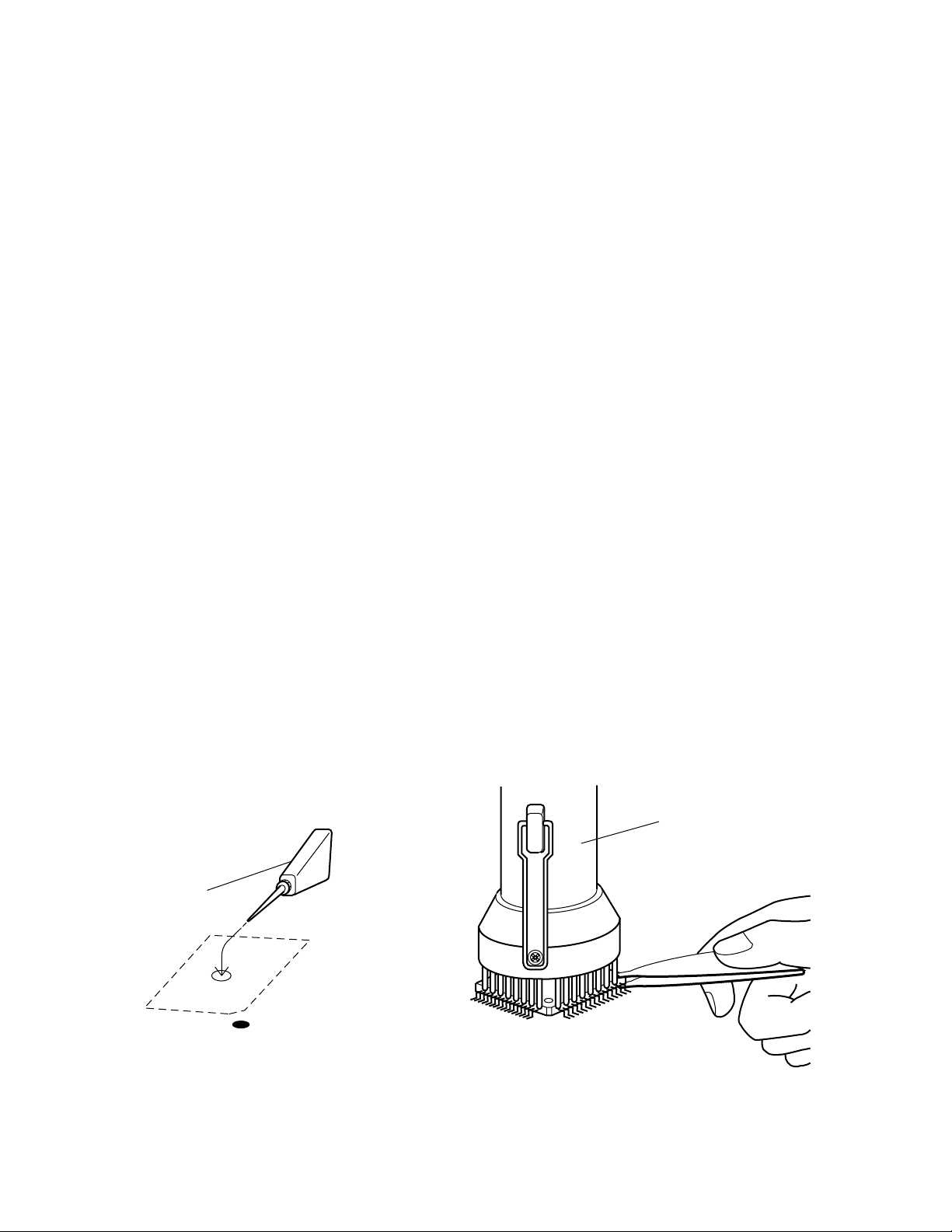
REPLACING THE DSP (HG51B155FD)
Note: To increase productivity ,the DSP HG51B155FD is sticked on the main PCB with a double-side
adhesive tape, then its leads are soldered.
Remove the DSP according to the following procedures.
1. Prepare isopropyl alcohol and a flat IC desoldering machine (Spot Heater HS-600).
2. Apply plenty of the alcohol to the adhesive tape from the reverse side of the main PCB. (Fig.1)
There is a hole on the PCB just under the LSI, and the adhesive tape can be seen through the hole.
3. Leave it more than one minute so that the alcohol weaken adhesive power fully.
4. Using a proper size of nozzle, apply heat to leads of the LSI with the desoldering machine.
5. Grasp the LSI with tweezers, and using gentle force vibrate the tweezers to feel melting solder. (Fig.2)
6. Remove the LSI after meltingsolder at every leads wholly.
Spot Heater HS-600
Alcohl
HG51A115A
LSI-S
— 2 —
Fig.2Fig.1
Page 5
BLOCK DIAGRAM
Keyboard
FI0 ~ FI7
SI0 ~ SI7
Key Touch LSI
LSI106
HG52E35P
KC0 ~
KC7
A0 ~ A2
Reset IC
IC104
RE5VA35AA
Working Strage
RAM (64K-bit)
LSI104
SRM2264LC90,10
A0 ~
A12
D0~D7
A0 ~ A14
Q109 ~ Q116
A0 ~ A3
La ~ Lg, Lp
LED driver
LD0 ~ LD7
RESET
CPU
LSI102
HD6433298A36P
7-Seg.
LED
LEDs
CLK
KO
LC1 ~ LC4
LO0 ~ LO4
KO Signal
Generator
IC303/304
TC74HC174P
KI1 ~ KI7
POWER
Power Switch
LED driver
IC301/302
BA612
KO0 ~ KO10
Buttons
VDD
MIDI
OUT
IN
Effect RAM
(64K-bit)
LSI107
SRM2264LC90,10
Speakers
EA0 ~ EA12
ED0 ~ ED7
Output
DSP
LSI105
HG51B155FD
WCK1 SLOP BCK
D/A Converter
LSI101
UPD6376CX
Filter
IC105
Main
Volume
Power Amplifier
IC102
LA4598
Filter
IC105
RA0 ~ RA19
RD0 ~ RD15
VC
Sound Source ROM
(16M-bit)
LSI103
TC5316200CP-C106
APO
LVDD
VCC
Power Supply Circuit
AVDD
IC101, Q1 ~ Q4
DVDD
VDD
— 3 —
Page 6
CIRCUIT DESCRIPTION
Key Matrix
KC0 KC1 KC2 KC3 KC4 KC5 KC6 KC7
FI0 C2 1 C#2 1 D2 1 D#21 E2 1 F2 1 F#21 G2 1
SI0 C2 2 C#22 D2 2 D#22 E2 2 F2 2 F#2 2 G2 2
FI1 G#21 A2 1 A#2 1 B2 1 C3 1 C#3 1 D3 1 D#3 1
SI1 G#22 A2 2 A#2 2 B2 2 C3 2 C#32 D3 2 D#32
FI2 E3 1 F3 1 F#3 1 G3 1 G#31 A3 1 A#3 1 B3 1
SI2 E3 2 F3 2 F#3 2 G3 2 G#32 A3 2 A#3 2 B3 2
FI3 C4 1 C#4 1 D4 1 D#4 1 E4 1 F4 1 F#4 1 G4 1
SI3 C4 2 C#4 2 D4 2 D#4 2 E4 2 F4 2 F#4 2 G4 2
FI4 C4 1 C#4 1 D4 1 D#4 1 E4 1 F4 1 F#4 1 G4 1
SI4 C4 2 C#4 2 D4 2 D#4 2 E4 2 F4 2 F#4 2 G4 2
FI5 E5 1 F5 1 F#5 1 G5 1 G#51 A5 1 A#5 1 B5 1
SI5 E5 2 F5 2 F#5 2 G5 2 G#52 A5 2 A#5 2 B5 2
FI6 C6 1 C#6 1 D6 1 D#6 1 E6 1 F6 1 F#6 1 G6 1
SI6 C6 2 C#6 2 D6 2 D#6 2 E6 2 F6 2 F#6 2 G6 2
FI7 G#61 A6 1 A#6 1 B6 1 C7 1
SI7 G#62 A6 2 A#6 2 B6 2 C7 2
Note: Each key has two contacts, the first conatct 1 and second contact 2 .
Key
FI
Second contact 2
First contact 1
KC
SI
Nomenclature of Keys
C#2
F#2D#2
C#3A#2G#2
D#3
F#3 G#3
A#3 C#4 D#4
F#4 G#4
A#4
C#5
D#5
F#5 G#5
A#5
C#6
G#6F#6D#6
A#6
C2 D2E2F2
G2
A2 B2 C3 D3
E3
F3 G3 A3 B3 C4 D4 E4 F4 G4 A4 B4 C5 D5 E5 F5 G5 A5 B5
— 4 —
C6
B6A6G6F6E6D6
C7
Page 7
Button Matrix
KI1 KI2 KI3 KI4 KI5 KI6 KI7
KO0 Registration 3 2 1 0
KO1 Control Demo Layer Split
KO2 Tone Rhythm 9 8 7 +
KO3 Accomp 6 5 4 -
Transpose/
Tune
Magical
Preset
Digital
Effect
Memory
Touch
Response
KO4 G# down A down A# down B down G down
KO5 ScaleMode ScaleTune B up A# up A up G# up G up
Song
KO6 Intro Start/Stop
Tempo
Down
Tempo
Up
Synchro/
Ending
Variation/
Fill-In
Normal/
Fill-In
KO7 C up C# up D up D# up E up F up F# up
KO8 C down C# down D down D# down E down F down F# down
KO9 Mode Pad B Pad D Pad A Pad C
KO10 Rec
Scale
Memory 1
Scale
Memory 2
Scale
Memory 3
Scale
Memory 4
Reset Circuit
Initial reset
When batteries are set or an AC adapter is connected, the reset IC provides a low pulse to the CPU.
The CPU then initializes its internal circuit and clears the working strage RAM.
Power ON reset
When the power switch is pressed, the CPU receives a low pulse of POWER signal. The CPU provides
APO signal to the power supply circuit, then provides RESET signal to the DSP, the key touch LSI and
the KO signal generators.
VDD
From power switch
Battery set
Reset IC
IC104
RE5VA35AA
RESET
POWER
VDD
CPU
LSI102
HD6433298A36P
-NMI
-RESET
DVDD
KO Signal Generator
IC303/304
TC74HC174P
Working Strage RAM
LSI104
SRM2264LC90,10
HG51B155FD
VDD
Key Touch LSI
LSI106
HG52E35
DVDD
DSP
LSI105
DVDD
— 5 —
Page 8
CPU (HD6433298A36P)
The 16-bit CPU contains a 32k-bit ROM, a 1k-bit RAM, seven 8-bit I/O ports, an A/D convertor and serial
interfaces. The CPU accesses to the working strage RAM, the DSP and the key touch LSI. The CPU also
controls buttons, bender input, LEDs and MIDI input/output.
The following table shows the pin functions of the CPU.
Pin No. Terminal In/Out Function
1 P40 Out KO signal data output
2 P41 Out Clock for KO signal data
3 P42 Out APO (Auto Power Off) signal output. ON: High OFF: Low
4 P43 Out Read enable signal output
5 P44 Out Write enable signal output
6 P45 Not used
7 P46 Out 10 MHz clock output
8 P47 In Wait signal input. Connected to +5 V.
9 TXD Out MIDI signal output
10 RXD In MIDI signal input
11 P52 Out Reset signal output
12 -RESET In Reset signal input
13 -NMI In Power ON signal input
14 VCC In +5 V source
15 -STBY In Standby signal input. Connected to +5 V.
16 VSS In Ground (0 V) source
17, 18 XTAL,EXTAL In 20 MHz clock input
19, 20 MD1, MD0 In Mode selection input.(Internal ROM mode --- MD1: High MD0: Low)
21 AVSS In Ground (0 V) source for the built-in DAC
22 AN0 In Analog input. Connected to ground.
23 ~ 29 P71 ~ P77 In Ternimal for button input signal
30 AVCC In +5 V source for the built-in DAC
31 ~ 38 P60 ~ P67 Out LED segment signal output
39 VCC In +5 V source
40 P27 Not used
41 ~ 56 P26 ~ P10 Out Address bus
48 VSS In Ground (0 V) source
57 ~ 64 P30 ~ P37 In/Out Data bus
Digital Signal Processor (HG51B155FD)
Upon receipt of note numbers and their velocities, the DSP reads sound and velocity data from the sound
source ROM in accordance with the selected tone; the DSP can read rhythm data simultaneously when a
rhythm pattern is selected. Then it provides 16-bit serial signals containing data of the melody, chord,
bass, and percussion to the DAC. The DSP also adds the selected effect to the sound data using a 64k-bit
RAM.
The following table shows the pin functions of the DSP.
— 6 —
Page 9
Pin No. Terminal In/Out Function
1 ~ 8 CD0 ~ CD7 In/Out Data bus
9, 10 Not used
11 GND7 In Ground (0 V) source
12 CK16 Out 16.384 MHz clock output
13 VCC6 In +5 V source
14 CK0 In Clock input. Connected to terminal CK16.
15 TCKB Not used
16 VCC1 In +5 V source
17 GND1 In Ground (0 V) source
18, 19 XT0, XT1 In/Out 16.384 MHz clock input/output. Connected to a crystal oscillator.
20 SGL In System control terminal. Single chip system: Open
21 CCSB In Chip select signal input
22 ~ 25 CA0 ~ CA3 In Address bus
26 CE0 In Not used. Connected to ground.
27 CWRB In Write enable signal
28 CRDB In Read enable signal
29 ~ 32 Not used
33 RESB In Reset signal input
34 TESB In Not used. Connected to +5 V.
35 ~ 39 Not used
40 ~ 49
52 ~ 57
RD0 ~ RD15 In Address bus for the sound source ROM
50 VCC2 +5 V source
51 GND2 Ground (0 V) source
58 RA23 Out Not used
59 RA22 Out Chip select signal for the sound source ROM
60, 61 RA20, RA21 Out Not used
62 ~ 73
75 ~ 82
RA0 ~ RA19 Out Address bus for the sound source ROM
74 GND5 In Ground (0 V) source
83 WOK2 Out Word clock output. Not used.
84 VCC3 In +5 V source
85 GND3 In Ground (0 V) source
86 WOK1 Out Word clock for the DAC
87 SOLM Out Serial data output. Not used.
88 SOLP Out Serial sound data output for the DAC
89 BOK Out Bit clock output for the DAC
90 ~ 92 Not used
93 VCC5 In +5 V source
94 EA14 Out Not used
95, 97
99 ~ 105
107, 109
EA0 ~ EA12 Out Address bus for the effect RAM
110, 112
— 7 —
Page 10

DAC (UPD6376CX)
UPD6376CX is a two-channel 16-bit Digital to Analog Convertor consisting of resistor string, output
amplifier and zero offset circuit.
Pin No. Terminal In/Out Function
1 SEL In Mode selection terminal. Connected to ground.
2 D.GND In Ground (0 V) source for internal digital circuit
3 NC Not used
4 DVDD In +5 V source for internal digital circuit
5 A.GND In Ground (0 V) source for internal analog circuit
6 R.OUT Out Right channel sound waveform output
7 A.VDD In +5 V source for internal analog circuit
8 A.VDD In +5 V source for internal analog circuit
9 R.REF In Reference voltage terminal. Connected to a capacitor.
10 L.REF In Reference voltage terminal. Connected to a capacitor.
11 L.OUT Out Left channel sound waveform output
12 A.GND In Ground (0 V) source for internal analog circuit
13 LRCK In Word clock (L/R separation signal) input.
14 LRSEL In Not used. Connected to ground.
15 SI In Sound data input
16 CLK In Bit clock input
Key Touch LSI (HG52E35P)
By counting the time between first-key input signal FI and second-key SI from the keyboard unit, the key
touch LSI detects key velocity of 256-step. Then the LSI sends the CPU the note number and its velocity
data.
Key touch LSI
RD
APO
WR
CLOCK
A12
A14
RESET
Data bus
Address bus
LSI106
HG52E35P
CRDB
CWRB
CKI
CCSB
RESB
CD0
CD7
CA0 ~ CA2
SI0
SI7
KC0
Key scan signal
~
KC7
FI0
Key input signal
FI7
Keyboard
KC
First contact
FI
SI
Second contact
— 8 —
Page 11

Pin No. Terminal In/Out Function
96 EWEB Out Write enable signal output for the effect RAM
98 EA13 Out Not used
106 EOEB Out Read enable signal output for the effect RAM
108 VCC7 In +5 V source
111 ECEB Out Chip select signal output for the effect RAM
113 ~ 117 Not used
118 VCC4 In +5 V source
119 GND4 In Ground (0 V) source
120 ~ 122 Not sued
123 ~ 130 ED0 ~ ED7 In/Out Data bus for the effect RAM
131 GND5 In Ground (0 V) source
132 ~ 134 Not used. Connected to ground.
135, 136 Not used
Block diagram of DSP and DAC circuit
Sound Source ROM
LSI103
TC5316200CP-C106
CE
A0 ~ A19 D0 ~ D15
RA22
RA0 ~
RA19
RD0 ~
RD15
SOLP: Sound data
BOK: Bit clock
WOK1: Word clock
A13
A14
RD
APO
WR
RESET
D0 ~ D7
A0 ~ A3
CCSB
CRDB
CWRB
ECEB EOEB
OE
CS
DSP
LSI105
HG51B155FD
EWEB
WE
ED0 ~
ED15
D0 ~ D15
EA0 ~
EA12
A0 ~ A12
Effect RAM (64K-bit)
LSI107
SRM2264LC90,10
SOLP
BOK
WOK1
DAC
LSI101
SI
CLK
LRCK
UPD6376CX
PG
X102
16.384MHz
ROUT
LOUT
— 9 —
Page 12

The following table shows the pin functions of the key touch LSI.
Pin No. Terminal In/Out Function
1 REQB Out Interrupt request. Not used.
FI8 ~ FI10
In Key input signal. Connected to + 5 V.2, 3, 60 ~ 63
SI8 ~ SI10
4 VCC In +5 V source
5 CRDB In Read enable signal
6 CWRB In Write enable signal
7 CCBB In Chip select signal
8, 9, 11 T, STBY, W In Not used. Connected to +5 V.
10 RESB In Reset signal
12 CKI In 10 MHz clock input
13, 14 TMD, TST In Not used. Connected to ground.
15 CKO Out Not used
16 GND In Ground (0 V) source
17 XIN In Not used. Connected to ground.
18 XOUT Out Not used
19 TRES In Not used. Connected to ground.
20 ~ 23, 25 ~ 28 CD0 ~ CD7 In/Out Data bus
24 GND In Ground (0 V) source
29 ~ 31 CR0 ~ CR2 In Address bus
32 VCC In +5 V source
33 ~ 39, 41 ~ 43 FI0 ~ FI7,
In Key input signal
53 ~ 55, 57 ~ 59 SI0 ~ SI7
40 VCC In +5 V source
44 ~ 47, 49 ~ 52 KC0 ~ KC7 Out Key scan signal
48, 56 GND In Ground (0 V) source
64 VCC In +5 V source
Filter Block
Since the sound signals from the DAC are stepped waveforms, the filter block is added to smooth the
waveforms.
10V22µ
To main volume
IC105
M5218APR
-
+
C333(H)
1K
C222(H)
AG
— 10 —
Q107/108
2SC1740
1K 1K
C103(H)
AG
AVDD
1K
AG
AVEE
18K
50V1µ
From the DAC
Page 13

Power Amplifier (LA4598)
The power amplifier is a two-channel amplifier with standby switch. The following figure shows the internal diagram of the amplifier.
Internal Diagram of LA4598
2
Ch2 B.S.
Ch1 IN
Ch1 N.F.
Pre GND
6
5
8
Input
Amp.
Pre-drive
Amp.
Power
Amp.
TSD protector
3
Ch1 OUT
1
Power GND
VCC
4
D.C.
Ch2 IN
Ch2 N.F.
7
10
11
Bias circuit
Input
Amp.
Pre-drive
Amp.
Stand by
Power
Amp.
9
Standby
Ch2 OUT
12
13
Ch2 B.S.
Power Supply Circuit
The power supply circuit generates six voltages as shown in the following table. VDD voltage is always
generated. The others are controlled by APO signal output from the CPU.
Name Voltage For operation of
VDD +5 V CPU, Reset IC, Working strage RAM
DVDD +5 V DSP, Key controller, Sound source ROM, Effect RAM, DAC, KO siginal generator
AVDD +5 V DAC Filter
LVDD +4.5 V LED Driver
VCC +9 V Pilot lamp
VC +9 V Power amplifier
— 11 —
Page 14

Bender
Volume
WIRING DIAGRAM
JCM719-CN2M
JG1
JG2
JG3
JG4
JG5
JG6
Lp
LC3
JG3
JC10
JC11
LC4
JG4
JG5
JC12
LgLfLe
JG6
JC1
JC2
JC3
JC4
JC5
LC1
LC2
JG1
JG2
JCM719-CN1M
JC6
JC7
JC8
JC9
JG7
JG7
JG8
JG9
LdLcLb
JG8
JD1
JG9
JG10
JG10
JD2
JG11
JG11
JD3
JG12
La
JG12
JD4
JD5
JD6
JD7
JD8
JD9
JD10
JD11
JD12
BATT+
BATT-
DG
DVDD
BENDER
JF3
JF2
JF1
JE5
JE4
JE3
JE2
JE1
AG
L OUT
R OUT
R IN
L IN
DC JACK
PHONE/OUTPUT
ASSIGNABLE JACK
MIDI IN
MIDI OUT
JA1
JA2
JA3
JA4
JA5
JA6
JE5
JE4
JE3
JE2
JE1
JA7
LG
PWLD
JC1
JC2
JCM719-MA2M
JA8
JA9
JA10
JA11
KI1
KI2
KI3
KI4
JC5
JC6
KI5
JC7
POWER
JC3
JC4
Main Volume
JA12
JA13
JA14
JA15
JA16
Lc
JD1
JC8
KI6
JC9
KI7
JC10
La
JC11
Lb
JC12
JCM719-MA1M
JB1
JB2
JB3
JB4
Ld
LeLfLg
JD2
JD3
JB5
JB6
JD4
JB7
JD5
JB8
Lp
JD6
JB9
CLK
JD7
JB10
KO9
JD8
JB11
KO
JD9
JB12
DVDD
RESET
JD10
JD11
JB13
JB14
DG
JD12
JB15
JB16
BATTERY
COMPARTMENT
FI1
JA1
FI2
FI0
SI0
SI1
JA2
JA3
JA4
JA5
M617T-KY1M
SI2
JA6
SI3
JA7
FI3
JA8
KC0
JA9
KC1
JA10
KC2
JA11
KC3
JA12
KC4
KC5
JA13
JA14
— 12 —
KC6
JA15
KC7
JA16
KC0
JB1
KC1
KC2
KC3
KC4
JB2
JB3
JB4
JB5
M617T-KY2M
KC5
JB6
FI4
JB7
SI4
JB8
KC6
JB9
KC7
JB10
SI5
JB11
SI6
JB12
JB13
SI7
FI5
JB14
FI6
JB15
FI7
JB16
Page 15

MAJOR WAVEFORMS
F
F Button scan signal KO0
IC304: TC74HC174AP pin 2
G Button scan signal KO1
IC304: TC74HC174AP pin 5
G
H
I
H Button scan signal KO2
IC304: TC74HC174AP pin 7
I Button scan signal KO3
IC304: TC74HC174AP pin 15
J DAC output
UPD6376CX pin 11
K DAC output
UPD6376CX pin 6
J
K
Tone: No. 78
Key: A4
Touch response: OFF
Digital effect: OFF
Volume: Maximum
1
2
1 Main clock pulse
HD6433298A36P pin 7
2 DSP clock pulse
HG51B155FD pin 12
Power switch ON
3
4
5
3 POWER signal
HD6433298A36P pin 13
4 APO signal
HD6433298A36P pin 3
5 RESET signal
HD6433298A36P pin 11
B
C
D
E
B Bit clock BOK
UPD6376CX pin 16
C L/R clock WOK1
UPD6376CX pin 13
D Sound data SOLP (Note OFF)
E Sound data SOLP (Note ON)
UPD6376CX pin 15
6
7
6 LED segment signal LD0
7 LED segment signal LD3
HD6433298A36P pin 31
HD6433298A36P pin 34
Display: "0.0"
8
9
0
A
8 Key scan signal KC0
HG52E35P pin 44
9 Key scan signal KC1
HG52E35P pin 45
0 Key scan signal KC2
HG52E35P pin 46
A Key scan signal KC3
HG52E35P pin 47
L
M
L Power amp. input
LA4598 pin 10
M Power amp. input
LA4598 pin 6
— 13 —
Page 16

D104
PS
JF
W
O
L104
3
2
EF101
1
1
15
JE
W
0
321
EF102
NO.
175
JE
5
5
75
L103
FB111
GR
C105
Q102
R104
R105
C121
J101
L121
5
125
75
C101
Q101
E
JF
5
75
B
D111
R103
R102
E
VCC
E
Q104
D112
5
D105
C120
R127
R132
1
1
JE
JE
5
5
3
312
VR101
D103
R111
C113
E
C103
C112
E
150
E
Q103
B
R291
R110
AVDD
DVDD R106
D101
75
VC
100
150
R114
R113
C116R117
R292
C111
C110
300
250
GR
3
3
MAIN VOL
Q105
L101
L102
C212
FB102
J102
L106
C115
C114
R112
R116
R115
100
C108
C127
300
300
175
175
150
Q122
BE
Q121
BE
R294
C211
5
R108
D107
E
BK
BK R
FB103
R118
100
5
R293
C104
PZ
C117
C107
IC102
5
IC101
C140
B
C182
L107
D109
R134
R
J103
100
C123
31
C145
5
C138
R295
R147
D102
150
C139
R148
C213
C171
FB104
C124
R120
C125
5
C126
R121
R126
C119
R125
C118
R124
R123
C131
R129
C130
R128
R131
R130
C128
C155
C143
C164
C102
R149
VDD
C146
IC104
R138
31
C132
C159
R173
R166
5
R184
R183
R182
R181
R155
R135
LSI101
C160
75
R174
R177
R156
C135
R136
C168
R176
100
C166
Q109
R157
12
202123 23
FB107
C137
C171
C161
75
C176
C196
175
B
E
R158
121
100
R190
R140
R143
C170
R199
R198
R197
4
3
6
E
Q110
R141
R139
75
150
R185
75
1
5
7
B
R191
R142
175
IC107
Q111
1
J104
C136
225
175
B
E
R200
Q112
MC102
1
C214
125
5
C185
R195
R194
R193
R192
LSI102
Q113
B
E
R201
75
R211R213
175
R212
LSI103
R214
150
300
200
200
C175
Q114
Q115
B
EB
E
R202
R203
C150
JD 12
LSI104
Q116
EB
R205
R204
EF103
JD
C149
C148
12
PCB VIEW AND MAJOR CHECK POINTS
R133
R162
R167
C153
R168
R163
X101
C156
D106
C165
C167
R150
C152
FB109
R178
R179
R180
75
R151
175
FB106
IC103
C162
R172
R171
75
FB110
MC101
R152
R153
JC
R159
R161
100
R175
R154
R165
125
125
5
100
5
R144
C129
IC105
100
125
R137
Q106
1
L108
C122
R160
Q108
C154
C174
R169
D108
C134
FB105
C133
Q107
BBEE
R164
R146
R145
C144
R170
C157
200
B
C141
C142
E
C147
JC
C173
C172
C163
75
C179
75
250
5
225
275
250
C180
C181
LVDD
75
EB
13 12
R186
R187
100
R188
125
C178
175
125
C197
100
IC106
5
C177
275
200
250
175
R206
C194
R245
R243
R268
R267
14 15
L110
C199
L111
100
100
C196
C186
R235
R269
1
100
100
100
100
R242
R270
C188
200
225
C195
LSI105
150
150
150
C191
C190
C189
125
100
C184
R210
225
C193
R216
FB114
FB113
R217
X102
175
150
5
5
5
5
5
5
100
100
R209
R208
FB112
300
75
75
R215
R220
R221
R222
R223
R224
R225
R226
R227
R228
R229
R230
C192
R219
75
R207
100
LSI106
R218
C187
250
150
R231
R232
R233
R234
R236
125225
R244
R271
125
1JA16
JA
16
R274
LSI107
150
R250
R237
R238
R241
275
R246
R247
R272
R273
C200
R249
C198
R240
R248
R275
5
R264
R265
R251
R252
R253
R254
R255
R256
R257
R258
R259
R260
R262
R263
R266
R239
R283
R282
R281
R280
R279
R278
R277
R276
75
R261
W
W
PR
BL
BL
2
1
JB
1
JB
5
17
17
— 14 —
Page 17

PCB JCM719-MA1M
SCHEMATIC DIAGRAMS
21
20
12
13
22
23
14 15
1
4
2
3
5
8 9 10 11
6 7
— 15 —
Page 18

PCBs JCM719-CN1M, CN2M, MA2M
19
16 17
18
— 16 —
Page 19

PCBs JCM617T-KY1M, KY2M
— 17 —
Page 20

EXPLODED VIEW
7
10
8
10
S-1
9
16
S-1
15 17
14
21
11
12
13
18
17
19
S-3
3-1
20
3
22
S-2
3-1
2
2-1
— 18 —
26
S-2
25
27
S-1
4
23
24
24
S-2
1
28-3
S-1
28-2
28-5
28
28-4
S-5
30
28-1
6
29
6-1
S-4
5-1
5
32
S-4
31
S-5
Page 21

IC LEAD IDENTIFICATION AND INTERNAL DIAGRAM
UPD6376CX
VDD
VSS
LRCK
LRSEL/RSI
SI/LSI
CLK
4/8 fs SEL
D.GND
MAIN DAC
13
54
A.GND
SUB DAC
SUB DAC
MAIN DAC
712
A.VDD
14
15
TIMING
16
1
2
GENERATOR
3
N.C.
SHIFT REGISTER
LATCH
D.VDD
11
L.OUT
10
L.REF
R.REF
9
6
R.OUT
8
RE5VA35AA
2
1
OUT
3
1 2 3
1A
2Y
3A
GND
1Y
2A 3
3Y
TC74HC04AP
1
2
4
5
6
7
14
12
11
10
M5218APR PC900V
VCC
VCC
6A13
8
VCC
67
5
6
-
+
-
6Y
+
GND
5A
12
34
12
5Y
9
4A
4Y
8
GND
45
NC
3
— 19 —
Page 22

BA612
TC74HC174AP
NC
I1
I2
I3
I4
I5
GND
Q1
D1
D2
Q2
D3
Q3
1
R
D
CK
D
CK
D
CK
Q
R
Q
R
Q
CK
D
CK
D
CK
R
D
Q
R
Q
R
Q
2
3
4
5
6
7
8
2SB1274
1
2
3
4
5
6
7
14
13
12
11
10
9
8
NC
O5
O4
O3
O2
O1
NC
CLEAR
GND
S-81350HG
16
15
14
13
12
11
10
9
VCC
Q6
D6
D5
Q5
D4
Q4
CLOCK
1 2 3
2SB1240Q,R
B C E
2SC1740SQ
2SA933SQ
DTA114TS
E C BE C B
— 20 —
Page 23

PARTS LIST
AT-1
Notes: 1. Prices and specifications are subject to change with-
out prior notice.
2. As for spare parts order and supply, refer to the
"GUIDEBOOK for Spare parts Supply", published
seperately.
3. The numbers in item column correspond to the same
numbers in drawing.
Page 24

FOB Japan
N Item Code No. Parts Name Specification Q N.R.Yen R
Unit Price
Main PCB JCM719-MA1M
N 1 6923 4040 PCB ass'y JCM719-MA1M M140127*1 1 B
LSI101 2011 3325 LSI UPD6376CX 1 A
N LSI102 2012 0021 LSI HD6433298A36P 1 A
N LSI103 2012 0035 LSI TC5316200CP-C106 1 A
LSI105 2011 7434 LSI HG51B155FD 1 A
LSI106 2011 5194 LSI HG52E35P 1 A
N LSI107 2012 0028 LSI SRM2264LC90,10 2 A
IC101 2105 2114 IC, Regulator S-81350HG 1 A
IC102 2114 2891 IC LA4598 1 A
IC103 2114 1421 IC, Photocoupler PC900V 1 A
N IC104 2105 3941 IC RE5VA35AA-TZ 1 A
IC105 2114 1799 IC M5218APR 1 A
IC106 2105 2912 IC HD74HC08P 1 A
IC107 2105 3136 IC HD74HC00P 1 A
Q101 2251 0665 Transistor 2SB1240R.S-TV6-T 1 A
Q102, Q104, 2252 0896 Transistor 2SC1740S-R,S-TP-T
6
Q107/108,
Q121/122
Q103 2251 0651 Transistor 2SB1274-CCC 1 A
Q105 2253 0455 Transistor 2SD1762E,F 1 A
Q106 2250 0574 Transistor 2SA933SQ,R-TP-T 1 A
Q109~116 2259 1883 Digital transistor DTA114TS-TP-T 8 A
D101 2360 2233 Zener diode RD5.1JSB1-T1-T 1 A
D102 2360 0098 Zener diode RD5.1ESB2-T1-T 1 A
D103 2390 0371 Diode DSK10B-BT-T 1 B
D104 2390 1316 Diode SB10-04A3-BT-T 1 B
D105/106, 2390 1344 Diode 1SS133T-77-T
5
D108,
D111/112
D107 2310 7996 Zener diode RD4.7ESB2-T1-T 1 A
D109 2390 1995 Diode RB441Q-T77-T 1 B
X101 2590 1526 Ceramic oscillator EFO-EN2005C4 1 B
X102 2590 1519 Crystal oscillator HC-49U16384 1 B
MC101 2819 5552 Module Capacitor CNB7X102M 1 C
MC102 2845 0168 Module Capacitor CNB8X101K 1 C
FB102~114 2845 3220 Ferrite beads EXC-ELDR35V-T 13 C
EF101~103 3025 0826 EMI filter EXC-EMT222DT-T 3 C
J101 3501 7049 DC jack HEC2305-01-330 1 A
J102 3612 0665 Phone jack YKB21-5006 1 B
J103 3612 0789 Jack YKB21-5010 1 B
J104 3501 4816 DIN jack YKF51-5051 1 B
L101~104, 3841 0539 Inductor ELE-V100KR-T
10
L106~111
N L121 3841 1456 Coil CM08RB01 1 C
N
4317 5522 Blank PCB JCM719-MA1M M140129B-1
1
Volume PCB JCM719-MA2M
2 6923 4050 PCB ass'y M719-MA2M M440151*1 1 B
VR101 2765 1575 Slide volume EWA-MJ0S10B23 1
2-1 3719 2562 Ribbon cable M296D DF5H05130-MM
1C
N 4317 5532 Blank PCB JCM719-MA2M M140129B-2 1 C
Console PCB JCM719-CN1M
N 3 6923 4060 PCB ass'y M719-CN1M M140128*1 1 B
IC303/304 2105 3045 IC HD74HC174P 2 A
Notes: N – New parts
M – Minimum order/supply quantity
R – Rank
— 21 —
A
B
C
A
Page 25

FOB Japan
N Item Code No. Parts Name Specification Q N.R.Yen R
Unit Price
IC301/302 2114 3318 IC BA612 2 A
LED301~309, 2370 0343 LED LN28RPX-(TT)
LED311
LED309/310 2370 0959 LED LN882RPX-(TT) 2 C
N LED312 2370 1141 LED SL-9352-60 1 C
D301~368 2390 1344 Diode 1SS133T-77-T 68 C
3-1 3719 4235 Ribbon cable M711C DF5H12120-MM 3 C
N 4317 5540 Blank PCB JCM719-CN1M M140130-1 1 C
LED PCB JCM719-CN2M
N 4 6923 4070 PCB ass'y M719-CN2M M340168*1 1 B
N 2370 1148 LED LN28RPH(V)-(TA9) 27 C
N 4317 5550 Blank PCB JCM719-CN2M M140130-2 1 C
Keyboard PCBs
N 5 6923 6940 PCB ass'y M617T-KY1M M140211*1 1 B
2301 0101 Diode 1S2473-T-77-T 64 C
N 5-1 3719 4557 Ribbon cable DF5H16200-MM 1 C
N 4317 5560 Blank PCB M617T-KY1M M140200-1 1 C
N 6 6923 6950 PCB ass'y M617T-KY2M M140212*1 1 B
2301 0101 Diode 1S2473-T-77-T 58 C
N 6-1 3719 4564
N 4317 5570 Blank PCB M617T-KY2M M140201-1 1 C
Bender
2765 1141 Volume RK1631110-50KB 1 C
Mechanical Parts
N
N
N 13 6923 4300 Rubber button 711C M312124-2
N
N
N
N
N 26 6923 4410 Bender knob M340169-1 1 C
N 27 3719 4536 Ribbon cable M719F DF5H03095-35353535 1 C
N 28 6922 3925 Upper case sub ass'y M111732E*2 1 C
7 6923 4250 Display plate 719 M340042-1 1
8 6921 5040 Slide knob M311860-1
9 6923 4290 Panel 719 M140037-1 1
10 3831 0357 Speaker 1221AF
11 6922 3830 Rubber button 711A M312122-1
12 6922 3840 Rubber button 711B M312123-1
14 6923 4310 Rubber button 711F M211727-2 1
15 6923 4320 Rubber button 711E M312126-2 1
16 6922 2680 Rubber button 710D M312082-2
17 6922 3870 Rubber button 711D M312125-1
18 6922 2660 Rubber button 710C M312088-1
19 6923 4350 Rubber button 719A M340038-1 1
20 6923 4360 Rubber button 719B M340039-1 1
21 6922 2840 White key set CEGB M111723-1
22 6922 2860 White key set DFAS M111725-1
23 6922 2850 White key set DFA M111724-1
24 6922 2740 Black key set 10P M111726-1
25 6922 2750 Black key set 5P M111726-2
6911 5241 Bender chassis A M31487A-1 1 C
6911 5250 Bender chassis B M41946-1 1 C
6911 5260 Bender spring M41949-1 1 C
28-1 6902 6140 Battery spring 90 M41226-1 1 B
28-2 6903 2150 Battery spring B M41330-1 1 B
28-3 6922 2810 Lower key stopper 710 M412287-1 1 C
28-4 6922 2820 Upper key stopper 710 M412286-1 1 C
28-5 6922 4480 Key damper 710 M412324-1 1 C
Notes: N – New parts
M – Minimum order/supply quantity
R – Rank
Ribbon cable DF5H17200-MM
— 22 —
9
1C
1
2
1
1
1
1
2
1
5
1A
4A
2A
1A
C
C
B
C
B
B
B
B
B
B
B
B
B
B
B
A
Page 26

FOB Japan
N Item Code No. Parts Name Specification Q N.R.Yen R
Unit Price
29 6922 2761 Key contact rubber LT-CB M211704A-1 4 A
30 6922 2771 Key contact rubber LT-CS M211705A-1 1 A
31 6922 2631 Bottom plate 710 M211706A-1 1 C
N 32 6918 1636 Battery cover M311164F*1 1 B
N 6923 4280 Rating plate M312163-2 1 C
Accessory
6920 8680 Dust cover 590 M311784-1 1 B
6920 8691 Music stand 590 M311760A-1 1 B
Notes: N – New parts
M – Minimum order/supply quantity
R – Rank
Description of Capacitors
A general description of capacitors is shown in the following table.
The description consists of Type, Value, Rated Voltage and Tolerance.
When you need a capacitor, please find a subsutitution in your country by yourselves referring to the
description.
Ref. No of Capacitor Description
C101, C107, C125, C211 Electrolytic, 16 V, 470 µF, +/-20%
C110, C153 Electrolytic, 6.3 V, 220 µF, +/-20%
C103, C104, C113, C114, C121, C137~C139, C145, C167, C171, C193,
C197
C108 Electrolytic, 16 V, 10 µF, +/-20%
C152, C162 Electrolytic, 50 V, 1 µF, +/-20%
C111, C182 Electrolytic, 6.3 V, 470 µF, +/-20%
C102, C124, C126, C134, C159~C161 Electrolytic, 6.3 V, 100 µF, +/-20%
C123, C127 Electrolytic, 10 V, 100 µF, +/-20%
C144, C165 Semiconductive, 16 V, 2200 pF, +/-10%
C147, C164 Semiconductive, 16 V, 0.033 µF, +/-10%
C130, C131 Semiconductive, 16 V, 0.047 µF, +/-10%
C128, C129, C154, C174 Semiconductive, 16 V, 0.01 µF, +/-10%
C118, C119 Semiconductive, 16 V, 0.018 µF, +/-10%
C140, C155, C166, C170, C175~C179, C181, C185, C186, C188, C189,
C192, C194~C196, C198, C200
C105, C120, C132, C133, C135, C136, C141, C142, C146~C150, C163,
C172, C173, C180, C184, C187, C212~C214
C122, C199 Ceramic, 50 V, 1000 pF, +/-10%
C168 Ceramic, 50 V, 0.01 µF, +/-20%
C191 Semiconductive, 16 V, 33 pF, +/-10%
C156, C157 Semiconductive, 16 V, 4 pF, +/-0.5 pF
C190 Semiconductive, 16 V, 22 pF, +/-10%
C116, C117 Mylar, 50 V, 0.047 µF, +/-10%
C112, C115 Electrolytic, 10 V, 1000 µF, +/-20%
Electrolytic, 10 V, 22 µF, +/-20%
Ceramic, 50 V, 0.1 µF, +80/-20%
Ceramic, 50 V, 100 pF, +/-10%
— 23 —
Page 27

Description of Resistors
A general description of resistors is shown in the following table.
The description consists of Type, Value, Rated Wattage and Tolerance.
When you need a resistor, please find a subsutitution in your country by yourselves referring to the
description.
Note:
All resistors are carbon film, 1/5 watt, +/-5% otherwise specified.
Ref. No of Resistor Description
R107, R137, R145~R147, R150, R163, R164, R168~R170, R189 1 KΩ
R102, R103, R133, R135, R142 220 Ω
R220~R230 330 Ω
R132, R143, R159, R185, R292 10 Ω
R115, R116, R127, R139~R141, R149, R158, R166, R171~R173,
R186~R188, R206, R208~R211, R213, R215
R175, R212, R214 100 KΩ
R105, R138, R148, R161, R274, R293, R295 10 KΩ
R110, R291 22 Ω
R117, R118 3.3 Ω
R111~R114 82 Ω
R125, R126, R160 4.7 KΩ
R207 1.5 KΩ
R134 2.2 KΩ
R136 270 Ω
R106, R108, R151~R157, R165, R251~R273, R275~R283 470 Ω
R104, R294 47 KΩ
R178~R184, R218, R219, R231~R250 56 KΩ
R216 1 MΩ
R174, R176, R177, R192~R199 33 KΩ
R123, R124, R130, R131 15 KΩ
R128, R129 5.6 KΩ
R217 560 Ω
R162, R167 18 KΩ
R190, R191, R200~R205 33 Ω
R120, R121, R144 47 Ω
100 Ω
— 24 —
Page 28

8-11-10, Nishi-Shinjuku
Shinjuku-ku, Tokyo 160, Japan
Telephone: 03-3347-4926
May, 1995
 Loading...