

Canon PowerShot A30, PowerShot A40 Service Manual

Application
This manual has been issued by Canon Inc. for qualified persons to learn technical theory, and
repair of the products.
Corrections
This manual could include typographical errors or technical inaccuracies due to improvements or
changes in the products. When changes occur in applicable products or in the content of this manual,
Canon will release service manual report as the need arises. In the event of major changes in the
contents of this manual over a long or short period, Canon may issue new editions of this manual.
The following paragraph does not apply to any countries where such provisions are inconsistent
with local law.
Trademarks
The product names and company names described in this manual are the registered trademarks of
the individual companies.
Copyright
This manual is copyrighted with all rights reserved. Under the copyright laws, this manual may not
be copied, reproduced, published (including on the World Wide Web) or translated into another
language, in whole or in part, without the written consent of Canon Inc..
Copyright © 2002 by Canon Inc.
CANON INC.
Digital Imaging Products Service Dept.
30-2, Shimomaruko 3-Chome, Ohta-ku,
Tokyo 146-8501, Japan
SAFETY PRECAUTIONS
The following precautions should be observed when servicing.
1. Since many parts in the unit have special safety-related characteristics, always use genuine CANON replacement parts.
Especially critical parts in the power circuit block should not be replaced with other makes.
Critical parts are marked with ! in the schematic diagrams.
2. When servicing, observe the original lead dress. If a short circuit is found, replace all parts which have been overheated or damaged
by the short circuit.
3. After servicing, see to it that all the protective devices such as insulation barriers, insulation papers shields are properly installed.
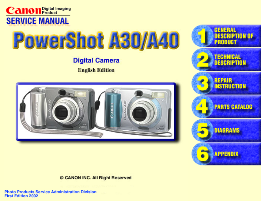
4. After servicing, make the following leakage current checks to prevent the customer from being exposed to shock hazards.
4-1 Leakage Current Cold Check
1) Unplug the AC cord and connect a jumper between the two prongs on the plug.
2) Measure the resistance value, with an ohmmeter, between the jumpered AC plug and each exposed metallic cabinet part
on the equipment such as screwheads, connectors, control shafts, etc. When the exposed metallic part has a return path to
the chassis, the reading should be between 1MΩ and 5.2MΩ. When the exposed metal does not have a return path to the
chassis, the reading must be ∞.
4-2 Leakage Current Hot Check
1) Plug the AC cord directly into the AC outlet. Do not use an isolation transformer for this check.
2) Connect a 1.5KΩ 10 watt resistor, paralleled by 0.15µF capacitor, between each exposed metallic parts on the unit and a
good earth ground such as a water pipe, as shown in the figure below.
3) Use an AC voltmeter, with 1000Ω/volt or more sensitivity, to measure the potential across the resistor.
4) Check all exposed metallic parts of the cover (Cable connection, Handle bracket, metallic cabinet.
Screwheads, Metallic overlays, etc), and measure the voltage at each point.
5) Reverse the AC plug in the AC outlet and repeat each of the above measurements.
6) The potential at any point should not exceed 0.75V RMS.
A leakage current tester (FLUKE MODEL : 8000A equivalent) may be used to make the hot checks.
Leakage current must not exceed 0.5 milliamp.
In case a measurement is outside of the limits specified, there is a possibility of a shock hazard, and corrective action must
be taken before returning the instrument to the customer.
AC OUTLET
DEVICE
UNDER
TEST
AC VOLTMETER
Test all
exposed
metal parts
Figure. 1 Leakage Current Hot Check
1.5KΩ
0.15µF
Water pipe
(Earth Ground)

CHAPTER 2. TECHNICAL DESCRIPTION
CONTENTS
1. Functions of each unit
1.1 MAIN PCB ASS’Y --------------------------------------------------------------------------------------------------------- 2-1
1.2 DC/DC PCB ASS’Y -------------------------------------------------------------------------------------------------------- 2-1
1.3 FLASH UNIT ---------------------------------------------------------------------------------------------------------------- 2-1
2. Outline of Circuits
2.1 Power Supply Control ------------------------------------------------------------------------------------------------------ 2-2
2.1.1 Power Supply Block Diagram ----------------------------------------------------------------------------------- 2-2
2.1.2 Power Control Sequence ------------------------------------------------------------------------------------------ 2-2
2.2 Signal Processing ------------------------------------------------------------------------------------------------------------ 2-3
2.2.1 System Control ----------------------------------------------------------------------------------------------------- 2-3
2.2.2 Picture Processing ------------------------------------------------------------------------------------------------- 2-4
2.2.3 Audio Processing (During record and playback) -------------------------------------------------------------- 2-4
3. Troubleshooting
3.1 When an Error Code is Displayed ---------------------------------------------------------------------------------------- 2-5
3.2 When a Problem Occurs ---------------------------------------------------------------------------------------------------- 2-7
1. Functions of each unit
1.1 MAIN PCB ASS’Y
1) Driving the CCD Sensor.
2) Conversion of the image signal from the analog signal to the digital signal.
3) Controlling the power supply and the system by CPU. (Refer to Sections 2.1 and 2.2.)
4) Image processing, and reading and writing the image signal to and from the CF card using DSP.
(Refer to Section 2.2.2.)
5) LCD drive and amplification of the video and audio output. (A40 model only) (Refer to Section
2.2.3.)
1.2 DC/DC PCB ASS’Y
1) Power supply drive (DC/DC converter).
2) Backlight for LCD drive.
1.3 FLASH UNIT
1) Flash drive and charging circuit for the flash.
CHAPTER 2. TECHNICAL DESCRIPTION
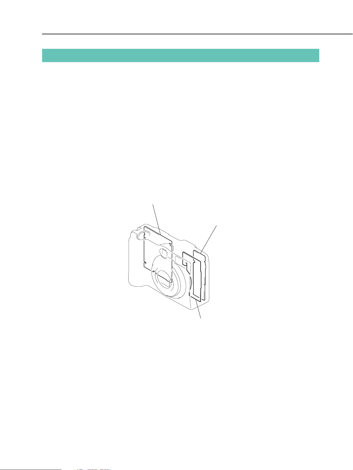
MAIN PCB ASS’Y
Fig. 1
DC/DC PCB ASS’Y
FLASH
UNIT
2-1
CHAPTER 2. TECHNICAL DESCRIPTION
2. Outline of Circuits
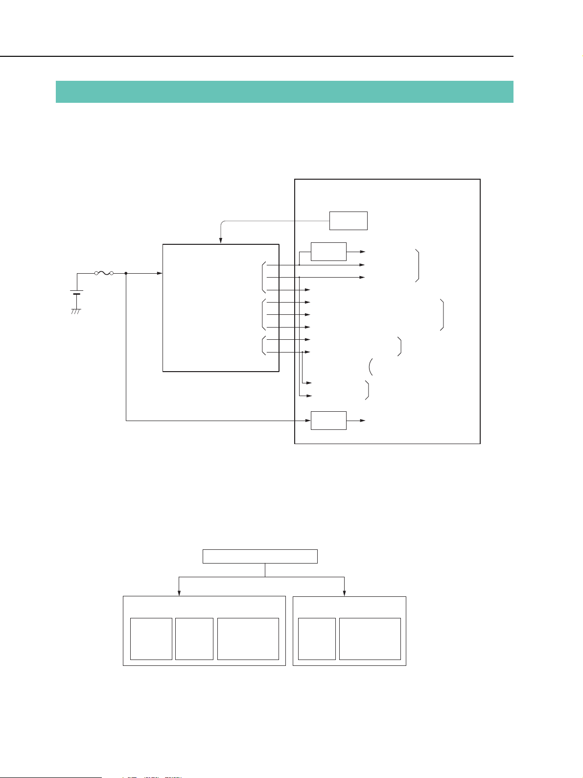
2.1 Power Supply Control
The power supply is controlled by the CPU mounted on the main PCB ass’y.
2.1.1 Power Supply Block Diagram
MAIN PCB ASS'Y
BATTERY
or
DC_IN
FUSE
VBATT
E1, E2, E3, E4
DC/DC
CONVERTER
E1
OUTPUT
E2
OUTPUT
E3 or E4
OUTPUT
CPU
REG
VCC1M (3.3V)
VDD2 (15V: A40 / 15.5V: A20 Model)
VEE2 (–7.5V: A40 / –8.0V: A20 Model)
VCC2 (4.2V)
VDD34 (13.5V)
VCC34 (4.2V: E3/5V: E4)
VCC34 (5V)
VCC1A (3.3V)
REG
Fig. 2 Power System Block Diagram
VCC1L (2.5V)
VCC1 (3.3V)
VCC1A (3.3V)
for Motor Drive
for LCD, VIDEO OUT
E3: LCD
E4: Video
for AUDIO OUT
(A40 Model Only)
(3.3V) for RTC
for System Control
for Image
Process
(CCD etc.)
2.1.2 Power Control Sequence
Main Switch ON (E1)
Shooting Mode Playback Mode
LCD OFF
(E2)
LCD ON
(E2, E3)
* A40 Model only
Audio*/Video
out (E2,E4)
2-2
LCD ON
(E3)
Audio*/Video
out (E4)
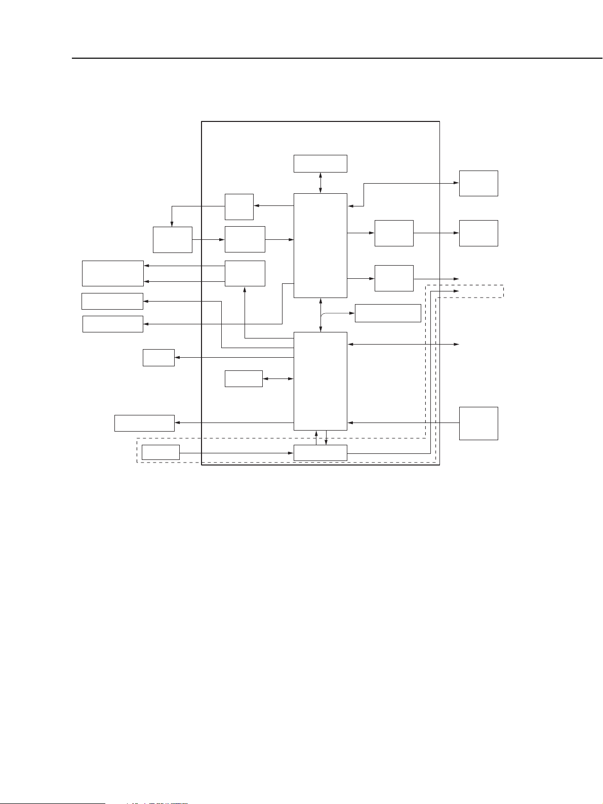
2.2 Signal Processing
MAIN PCB ASS'Y
CHAPTER 2. TECHNICAL DESCRIPTION
SDRAM
EF LENS
AF Support LED
FINDER LED
Electric FLASH
CCD
Sensor
Buzzer
MIC
(A40 Model Only)
TG
CDS, A/D
Motor
Driver
RTC
HD, VD
CLKDrive Pulse
DSP
CPU
AUDIO AMP
LCD
Driver
Video
Amp
FLASH MEMORY
CF card
LCD
VIDEO OUT
AUDIO OUT
USB
SW
DIAL
KEY
Fig. 3 Signal System Block Diagram
2.2.1 System Control
The CPU on the main PCB ass’y controls the EF lens (motor, shutter), operation switch receiver, USB
communication and flowing circuits.
• TG: Creation of the CCD drive pulse
• CDS, A/D: CCD signal processing and conversion of the digital data
• LCD Driver: Driving the LCD
• FLASH MEMORY: Firmware memory
• DSP: Picture processing
• RTC: Clock count for watch
• AF Support LED: AF auxiliary, self-timer and red-eye protection also serves as a lamp
• Electric Flash: Flash and charging circuit
2-3

CHAPTER 2. TECHNICAL DESCRIPTION
2.2.2 Picture Processing
1) The drive pulse of the CCD sensor is created by both clock from DSP and TG that is operated by
sync. signal.
The picture signal by the drive pulse is output from CCD sensor.
The output signal of the CCD picture is converted to the signal processing and the digital data by
the CDS and A/D converter, and is sent to the DSP.
2) The DSP circuit performs the following signal processing.
• Processes the picture data (using the SDRAM).
• Writes and reads the picture data to and from the CF card.
• Inputs the picture data to the CPU.
• Outputs analog video signal to the LCD and VIDEO OUT.
3) The video signal that is supplied form the DSP is controlled by the LCD driver and is displayed
on the LCD. The video amplifier is activated when the video jack is inserted to the video jack or
AV jack and drives the video signal in 75 Ω.
2.2.3 Audio Processing (During record and playback)
1) During animation recording.
• The microphone audio signal is converted to the digital data by CPU and is recorded.
2) During playback, the data is converted back to the analog audio signal and is output to the AV
jack.
Note: Installed in the A40 model only. (Audio cannot be played back by camera.)
2-4

CHAPTER 2. TECHNICAL DESCRIPTION
3. Troubleshooting
3.1 When an Error Code is Displayed
[Remedy]
• Check for any abnormalities in the mounting of probable faulty parts or connector connections referring
to the table below.
• Try replacing probable faulty parts referring to the below.
[NOTE]
• The error code is displayed on the LCD Monitor.
• Adjustments must be performed after the part has been replaced. For details, see the chapter of
“Adjustments”.
Error Code
E02
E03
E09
E14
E16
E18
E23
E24
E25
E26
Name
AF
TIME OUT
EF
TIME OUT
JPEG DMA
TIME OUT
UNKOWN
IMAGING TIME
OUT
ZOOM LENS
ERROR
CF NO SPACE
POWER ON
ERROR
FOCUS PI
ERROR
CAPTURE
TIME OUT
Occurrence Conditions
AF processing did not end within the
specified time.
The focus lens was not driven.
Auto Flash Control did not end within the
specified time.
JPEG processing did not end within the
specified time.
When unkown error, cause of which is
not known, occurs.
When communication between CPU and
peripheral IC is not completed within the
specified time during recording using
EVF or after completion of recording.
Movement of the lens barrel did not end
within the specified time.
When the CF becomes full during writing
of photographed images to CF, writing is
repeatedly performed with the JPEG
compression ratio successively increased
to reduce the size of the image file until it
can be successfully written to CF.
This error occurs when writing of the
JPEG image file fails after 10 retries at
increasingly higher compression ratios.
The power of the imaging circuit on the
MAIN PCB ASS’Y was not detected.
Detection of the focus PI (photo-
interrupter) failed.
Writing of the photograph image to
SDRAM did not end within the specified
time.
Cause and Probable Faulty Part
MAIN PCB ASS’Y
OPTICAL UNIT
MAIN PCB ASS’Y
OPTICAL UNIT
MAIN PCB ASS’Y
OPTICAL UNIT
MAIN PCB ASS’Y
UNKOWN
MAIN PCB ASS’Y
MAIN PCB ASS’Y
OPTICAL UNIT
MAIN PCB ASS’Y
MAIN PCB ASS’Y
DC/DC PCB ASS’Y
OPTICAL UNIT
MAIN PCB ASS’Y
MAIN PCB ASS’Y
2-5

CHAPTER 2. TECHNICAL DESCRIPTION
Error Code
E27
E30
E50
E51
E52
Name
CF WRITE
TIME OVER
POWER OFF
ERROR
CF FORMAT
ERROR
CF ACCESS
ERROR
QUICK REVIEW
ERROR
Occurrence Conditions
Free area could not be secured in the
buffer for the photograph image within
the specified time in the continuous
shooting mode.
The camera power was turned OFF while
the image was being recorded to the CF
Card. (The error code is displayed when
the camera is next turned ON.)
* This error may occur after E23.
The CF Card could not be formatted
properly.
When image data cannot be read from
CF normally.
Review of the photograph image failed.
Cause and Probable Faulty Part
CF CARD
MAIN PCB ASS’Y
The battery or DC plug was removed
while the image was being recorded to
the CF Card.
→ Remedy: Restart the camera.
CF CARD
CF CARD
MAIN PCB ASS’Y
2-6

CHAPTER 2. TECHNICAL DESCRIPTION
3.2 When a Problem Occurs
[Remedy]
• Check for any abnormalities in the mounting of probable faulty parts or connector connections referring
to the table below.
• Try replacing probable faulty parts referring to the table below.
[NOTE]
• Adjustments must be performed after the part has been replaced. For details, see the chapter of
“Adjustments”.
Problem (when an error code is not displayed)
The camera does not work.
The image is not displayed on the LCD Monitor.
The photograph image is abnormal.
The zoom does not function.
The Built-in Flash does not fire.
Video output is strange.
Communications with the personal computer is not possible.
The CF card or Micro Drives is not recognized.
Buttons/The Mode dial do not work.
Cause and Probable Faulty Part
MAIN PCB ASS’Y
REAR COVER UNIT
DC/DC PCB ASS’Y
BATTERY BOX UNIT
MAIN PCB ASS’Y
BUTTON PCB ASS’Y
LCD PANEL
BACK LIGHT UNIT
OPTICAL UNIT
MAIN PCB ASS’Y
OPTICAL UNIT
MAIN PCB ASS’Y
BATTERY BOX UNIT
REAR COVER UNIT
FLASH UNIT
DC/DC PCB ASS’Y
MAIN PCB ASS’Y
MAIN PCB ASS’Y
CF CARD
REAR COVER UNIT
MAIN PCB ASS’Y
REAR COVER UNIT
RLS PCB ASS’Y
2-7


CHAPTER 3. REPAIR INSTRUCTION
CONTENTS
1. Before Starting the Repair Work
1.1 Precaution on Flash High Tension Circuit ------------------------------------------------------------------------------- 3-1
1.2 List of Tools ----------------------------------------------------------------------------------------------------------------- 3-1
1.3 List of Supplies -------------------------------------------------------------------------------------------------------------- 3-1
1.4 Flexible Connectors --------------------------------------------------------------------------------------------------------- 3-2
2. Disassembly/Assembly
2.1 Procedure --------------------------------------------------------------------------------------------------------------------- 3-3
2.2 REAR COVER UNIT ------------------------------------------------------------------------------------------------------ 3-4
2.3 FRONT COVER UNIT, CF COVER ------------------------------------------------------------------------------------ 3-5
2.4 LENS BARREL SHEET, BATTERY COVER UNIT ----------------------------------------------------------------- 3-6
2.5 BACKLIGHT UNIT, LCD PANEL -------------------------------------------------------------------------------------- 3-7
2.6 MAIN PCB ASS’Y --------------------------------------------------------------------------------------------------------- 3-8
2.7 DC/DC PCB ASS’Y -------------------------------------------------------------------------------------------------------- 3-9
2.8 FLASH UNIT ---------------------------------------------------------------------------------------------------------------3-10
2.9 OPTICAL UNIT, FINDER UNIT -------------------------------------------------------------------------------------- 3-11
2.10 CCD UNIT ----------------------------------------------------------------------------------------------------------------- 3-12
2.11 BATTERY BOX UNIT, RLS PCB ASS’Y, LITHIUM BATTERY HOLDER-----------------------------------3-13
2.12 OPTICAL UNIT ---------------------------------------------------------------------------------------------------------- 3-14
2.13 Assembling the FINDER UNIT ------------------------------------------------------------------------------------------ 3-15
2.14 Screw List -------------------------------------------------------------------------------------------------------------------3-16
3. Adjustments
3.1 Replacement Parts and Adjustment Items ----------------------------------------------------------------------------- 3-17
3.2 Adjustment Tools ----------------------------------------------------------------------------------------------------------3-18
3.3 Before Starting Electrical Adjustments --------------------------------------------------------------------------------- 3-19
3.3.1 TWAIN Driver Installation --------------------------------------------------------------------------------------3-19
3.3.2 Installing the Adjustment Software --------------------------------------------------------------------------- 3-19
3.3.3 Preparation -------------------------------------------------------------------------------------------------------- 3-21
3.3.4 Starting up the Adjustment Software --------------------------------------------------------------------------- 3-22
3.3.5 Menu Window-----------------------------------------------------------------------------------------------------3-22
3.3.6 How to Use the Adjustment Software ------------------------------------------------------------------------- 3-22
3.4 Calibration ----------------------------------------------------------------------------------------------------------------- 3-23
3.4.1 Calibration -------------------------------------------------------------------------------------------------------- 3-23
3.5 Adjustment Procedure ----------------------------------------------------------------------------------------------------- 3-27
3.5.1 CCD Adjustment ------------------------------------------------------------------------------------------------- 3-27
3.5.2 Optical Unit Adjustment ---------------------------------------------------------------------------------------- 3-29
3.5.3 Imaging Process Adjustment ------------------------------------------------------------------------------------3-31
3.5.4 Pixel Dot Adjustment --------------------------------------------------------------------------------------------3-35
3.5.5 Flash Adjustment -------------------------------------------------------------------------------------------------3-37
3.5.6 Language (For Oth) ----------------------------------------------------------------------------------------------- 3-39
3.5.7 Language Settings ----------------------------------------------------------------------------------------------- 3-41

CHAPTER 3. REPAIR INSTRUCTION
1. Before Starting the Repair Work
Be sure to read the following precaution before starting the repair work.
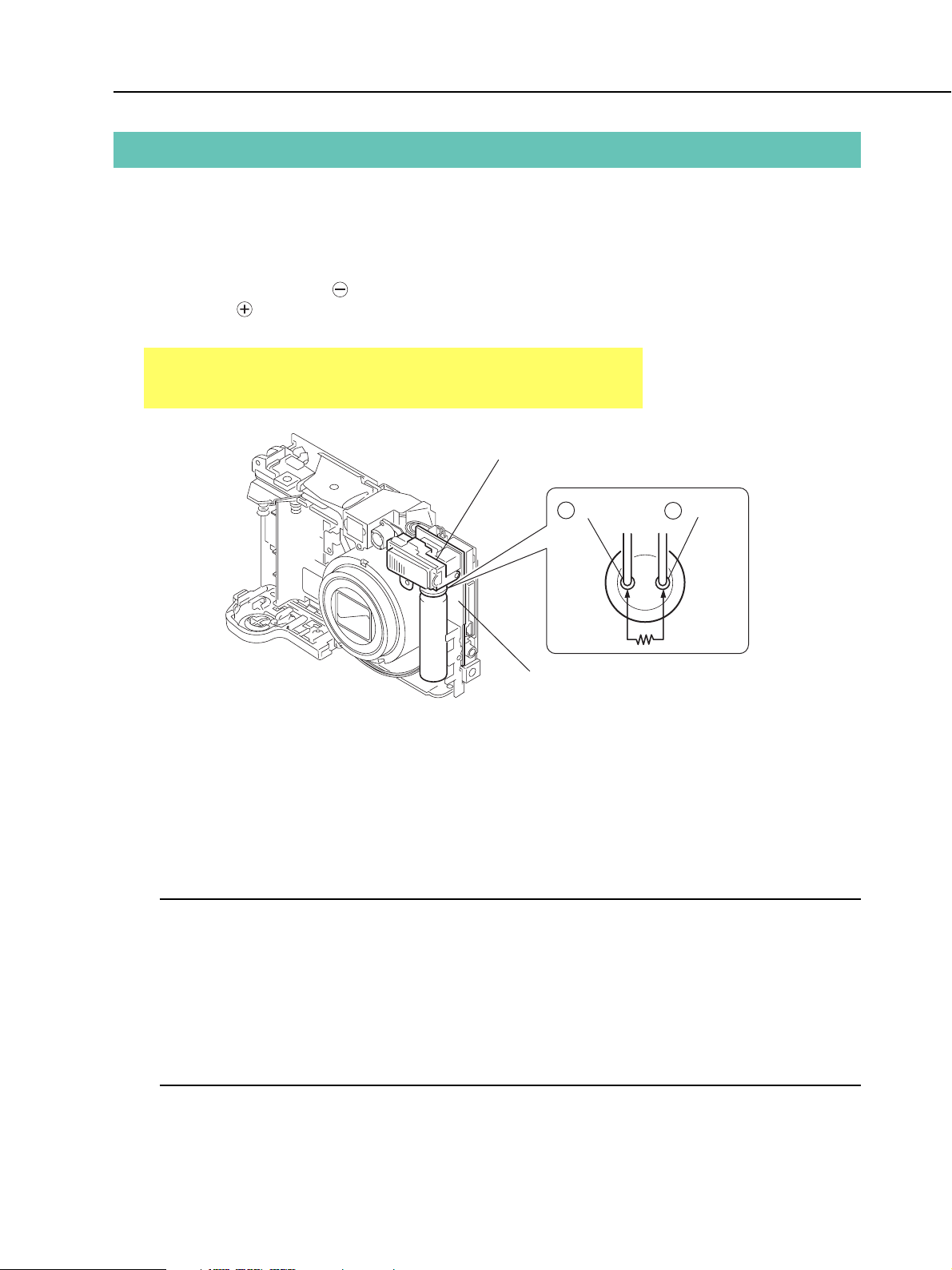
1.1 Precaution on Flash High Tension Circuit
• When the FRONT COVER UNIT is removed, be sure to discharge the main capacitor.
(Discharging resistor: 1 k ohms, approx. 5 W.)
• First contact the GND terminal of the main capacitor with the discharging resistor. Then contact the
positive terminal of the main capacitor.
CAUTION:
Be careful of electric shock because the circuit is the high tension circuit.
FLASH UNIT
Fig. 3-1 Precaution on flash high tension circuit
1.2 List of Tools
The following tools are used for the re-assembling during service.
(1) List of tools
New Name of tools Part No. Areas where supplies are used
DRIVER HANDLE CY9-7014-00 CCD UNIT
– terminal
DC/DC PCB ASS’Y
+ terminal
1.3 List of Supplies
The following supplies are used for the re-assembling during service.
(1) List of supplies
New Name of supplies Part No. Areas where supplies are used
DIA BOND 1663G CY9-8129-000 Attaching the parts together
ADHESIVE TAPE, SONY T4000 CY4-6012-000 Fixing the flexible cable
ADHESIVE TAPE, 3M NO.56 CY4-6018-000 DC/DC SHIELD CASE 1
3-1
CHAPTER 3. REPAIR INSTRUCTION
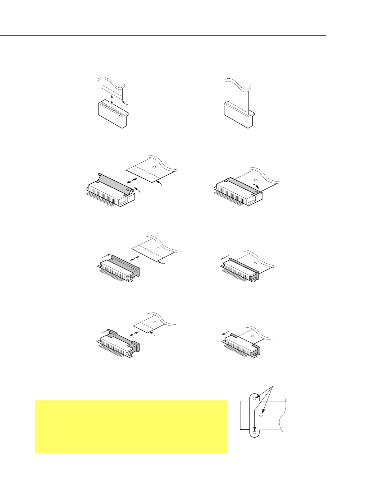
1.4 Flexible Connectors
This product uses the four types of the flexible connectors.
1 Type A
The contact-piece
should face
frontwards
Unconnected state Connected state
2 Type B
3 Type C
4 Type D
The contact-piece
UNLOCK
should face
downwards
Unlocked state Locked state
UNLOCK
The contact-piece
should face
downwards
LOCK
Unlocked state Locked state
UNLOCK
The contact-piece
should face
upwards
LOCK
Unlocked state Locked state
LOCK
Fig. 3-2 Flexible connectors
CAUTIONS:
1. For the connectors of Type B, Type C and Type D, set them to the
unlocked state before removing and inserting flexible card. After flexible card is inserted, set them to the locked state.
2. The flexible card is equipped with the holes as shown. Use them for
removal and insertion by inserting the tweezers into them as required.
3-2
Holes
Fig. 3-3 Holes for removal
CHAPTER 3. REPAIR INSTRUCTION
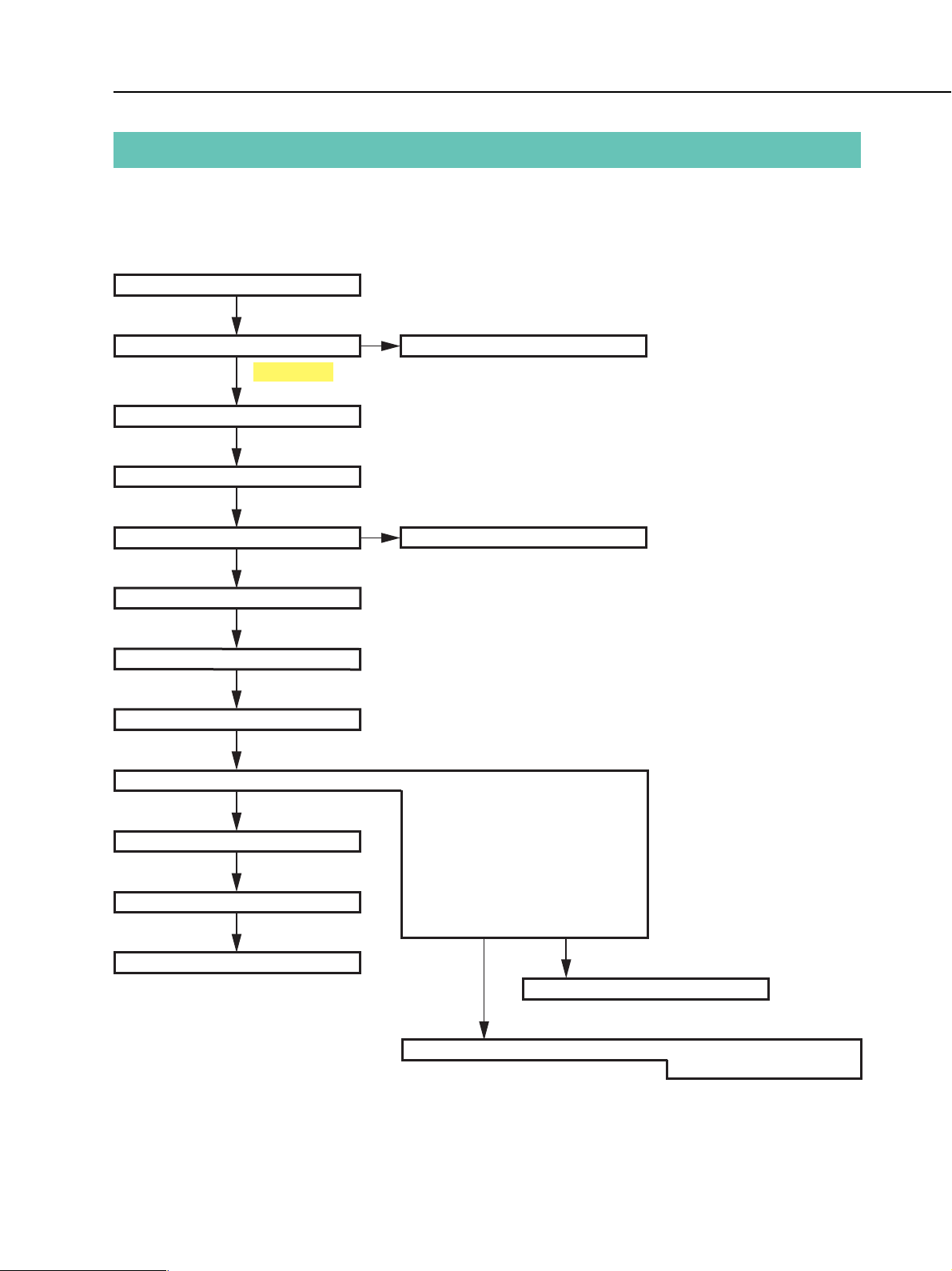
2. Disassembly/Assembly
2.1 Procedure
Disassembling procedure of PowerShot A40 (A30) is shown by the following flowchart.
Reverse the disassembling procedure to reassemble them. ∗ The pages to refer are shown in parenthesis ( ).
REAR COVER UNIT (3-4)
FRONT COVER UNIT (3-5)
CAUTION
Be careful high tension
LENS BARREL SHEET (3-6)
BATTERY COVER UNIT (3-6)
BACK LIGHT UNIT (3-7)
MAIN PCB ASS’Y (3-8)
DC/DC PCB ASS’Y (3-9)
FLASH UNIT (3-10)
OPTICAL UNIT (3-11)
BATTERY BOX UNIT (3-13)
RLS PCB ASS’Y (3-13)
CF COVER (3-5)
LCD PANEL (3-7)
LENS PLATE (3-14)
LENS BARREL CAP (3-14)
BARRIER CLOSE SPRING (3-14)
BARRIER PLATE 1 (3-14)
BARRIER PLATE 2 (3-14)
BARRIER PLATE 2 SPRING (3-14)
BARRIER BASE (3-14)
BARRIER OPEN SPRING (3-14)
BARRIER DRIVE RING (3-14)
LITIUM BATTERY HOLDER (3-13)
FINDER UNIT (3-11)
CCD UNIT (3-12)
3-3
CCD RUBBER (3-12)
IR FILTER (3-12)
CHAPTER 3. REPAIR INSTRUCTION
REAR COVER
UNIT
(1)-3
(1)-1
a
(1)-3
(1)-1
b
REAR COVER UNIT
a
(1)-1
(1)-2
(1)-1
CF COVER
a
(1)-1
b
b
(1)-1
CONNECTOR COVER
Fig. 3-4 REAR COVER UNIT
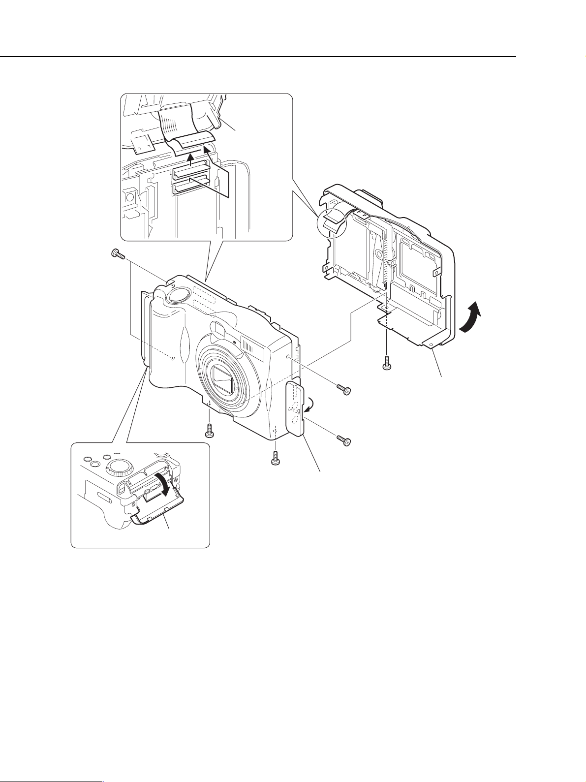
2.2 REAR COVER UNIT
(1) REAR COVER UNIT
1. Remove the six screws.
Remove the one screw by turning over the CONNECTOR COVER.
2. Open the CF COVER.
3. Open the REAR COVER UNIT in the direction of arrow and remove it by disconnecting the two flexible
printed wired board.
3-4
CF COVER
(1)-2
CHAPTER 3. REPAIR INSTRUCTION
(1)-2
BATTERY COVER UNIT
(1)-1
Fig. 3-5 FRONT COVER UNIT, CF COVER
2.3 FRONT COVER UNIT, CF COVER
(1) FRONT COVER UNIT, CF COVER
1. Open the BATTERY COVER UNIT after releasing the look while pushing the BATTERY OPEN
BUTTON in the direction of the arrow .
2. Take the FRONT COVER UNIT in the direction of arrow and at the same time remove the CF COVER.
3-5
CHAPTER 3. REPAIR INSTRUCTION
BATTERY COVER BAR
(1)-1
LENS BARREL SHEET
(2)-2
BATTERY COVER UNIT
(2)-1
BATTERY COVER
BAR
BATTERY COVER UNIT
Groove
NOTE (Assembling)
Lever block
BATTERY COVER UNIT
BATTERY COVER BAR
(Top view)
Fig. 3-6 LENS BARREL SHEET, BATTERY COVER UNIT
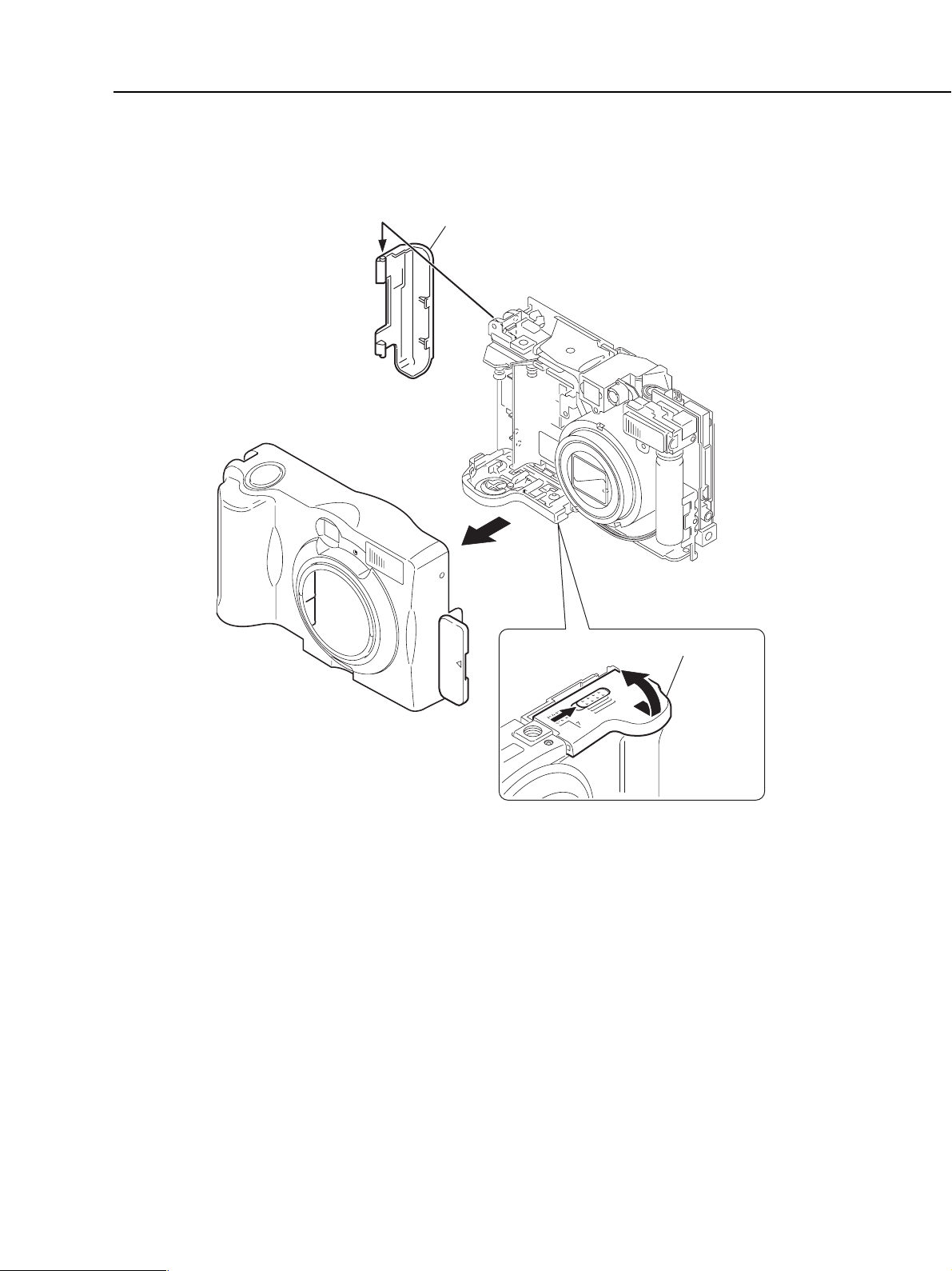
2.4 LENS BARREL SHEET, BATTERY COVER UNIT
(1) LENS BARREL SHEET
1. Remove the LENS BARREL SHEET.
(2) BATTERY COVER UNIT
1. Insert tweezers or the like into the groove of the BATTERY COVER BAR and remove it in the direction of
arrow.
2. Remove the BATTERY COVER UNIT.
NOTE (Assembling)
Attach the lever block to the BATTERY COVER UNIT.
3-6
(1)-4
CHAPTER 3. REPAIR INSTRUCTION
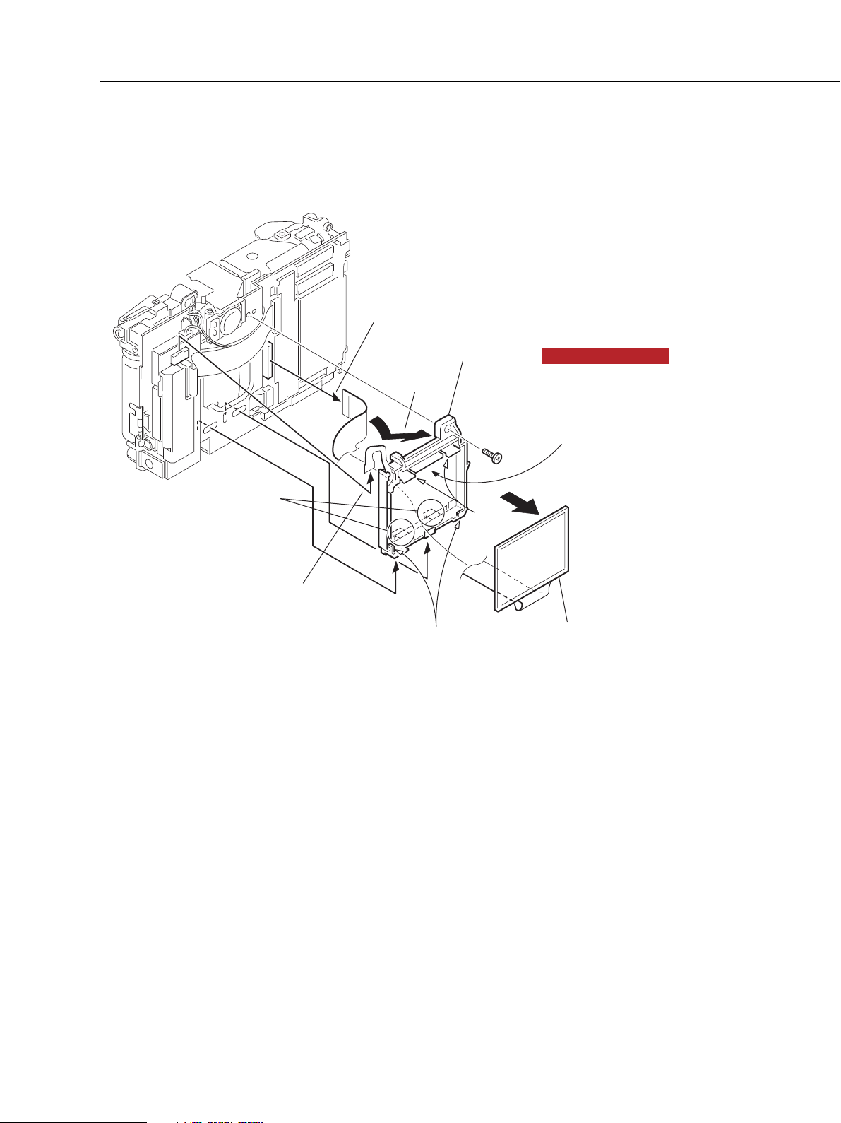
BACKLIGHT UNIT
(1)-3
(1)-2
Claws
Claws
(2)-1
(1)-1
(1)-3
Claws
(2)-1
Fig. 3-7 BACKLIGHT UNIT, LCD PANEL
NOTE (Assembling)
The BACKLIGHT UNIT that is
supplied as the service part has
the protection sheet on the back.
Remove it.
c
(2)-1
LCD PANEL
2.5 BACKLIGHT UNIT, LCD PANEL
(1) BACKLIGHT UNIT
1. Remove the flexible printed wired board of the BACKLIGHT UNIT.
2. Remove the screw.
3. Rotate the BACKLIGHT UNIT in the direction of arrow and remove it by releasing the claws.
4. Remove the flexible printed wired board of the LCD PANEL.
(2) LCD PANEL
1. Release the four claws in the top and bottom, and remove the LCD PANEL in the direction of arrow.
3-7
CHAPTER 3. REPAIR INSTRUCTION
How to fold the OPT FPC
OPT FPC
CCD UNIT FPC
(1)-1
EMC SHEET 2
(1)-2
d
M-S FPC
(1)-9
(1)-4
M-R FPC
(1)-3
Claws
(1)-8
(1)-10
(1)-6
(1)-5
M-D FPC
MAIN PCB ASS’Y
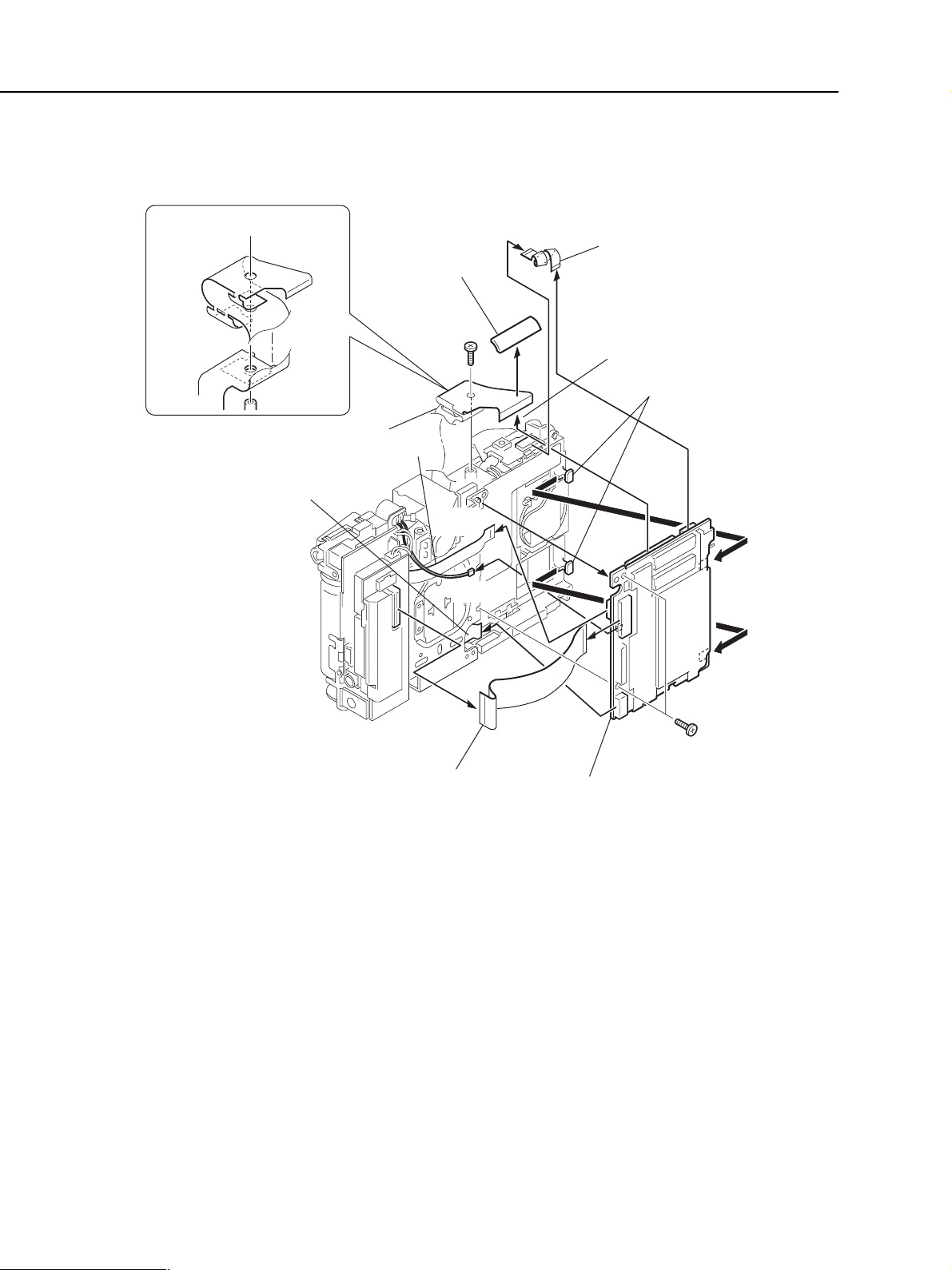
Fig. 3-8 MAIN PCB ASS’Y
2.6 MAIN PCB ASS’Y
(1) MAIN PCB ASS’Y
1. Remove the EMC SHEET 2.
2. Remove the screws.
3. Remove the OPT FPC.
4. Remove the M-R FPC.
5. Remove the M-D FPC.
6. Remove the flexible printed wired board of the CCD UNIT.
7. Remove the two screws.
8. While taking care of the claws in the top and bottom, remove the MAIN PCB ASS'Y
in the direction of arrow.
9. Remove the M-S FPC.
10. Disconnect the connector.
(1)-7
c
3-8
(1)-1
CHAPTER 3. REPAIR INSTRUCTION
(1)-1
(1)-3
NOTE (Assembling)
DC/DC SHIELD
CASE 1
Insulation tape
Fig. 3-9 DC/DC PCB ASS’Y
2.7 DC/DC PCB ASS’Y
(1) DC/DC PCB ASS’Y
1. Disconnect the two connectors.
2. Remove the two screws.
3. Remove the DC/DC PCB ASS’Y in the direction of arrow.
NOTE (Assembling)
Attach the insulation tape to the DC/DC SHIELD CASE 1.
(1)-2
c
DC/DC PCB ASS’Y
3-9
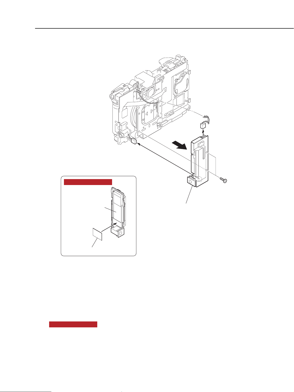
CHAPTER 3. REPAIR INSTRUCTION
(1)-2
Mold part
(1)-6
M-S FPC
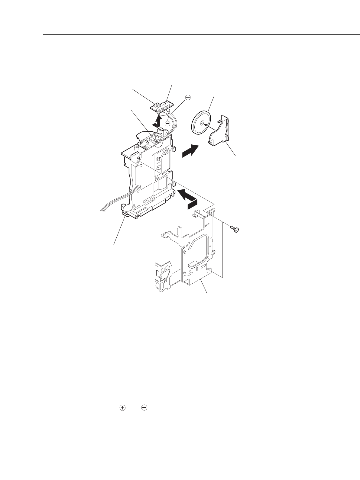
FLASH UNIT
(1)-5
EMS SHEET 1
c
(1)-3
c
(1)-3
(1)-4
Fig. 3-10 FLASH UNIT
2.8 FLASH UNIT
(1) FLASH UNIT
1. Remove the HIGH VOLTAGE CAUTION TAPE.
2. Remove the mold part of the FLASH UNIT from the dowel with the sharp point tweezers or the like.
3. Remove the two screws. (One screw from the front and the other from the rear.)
4. Remove the FLASH UNIT by sliding it.
5. Remove the EMS SHEET 1.
6. Remove the M-S FPC.
3-10
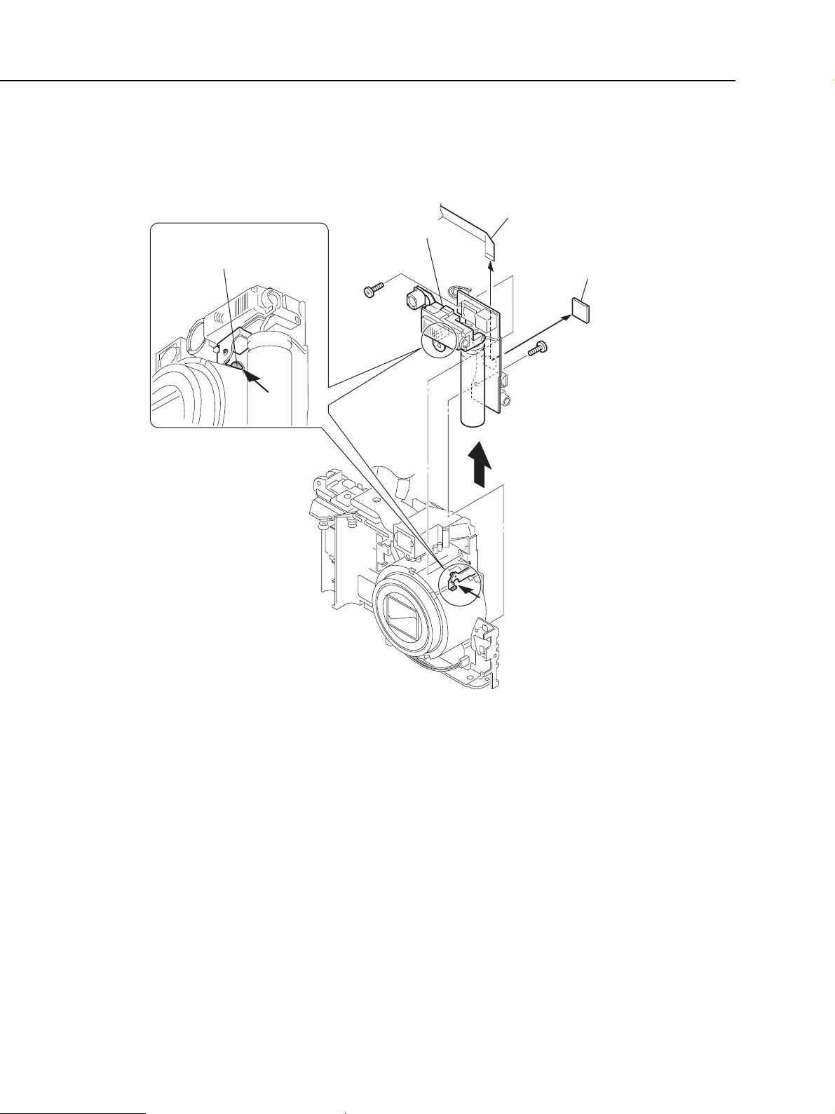
CHAPTER 3. REPAIR INSTRUCTION
e
FINDER UNIT
OPTICAL UNIT
(2)-3
e
(2)-2
(2)-1
(1)-2
(1)-1
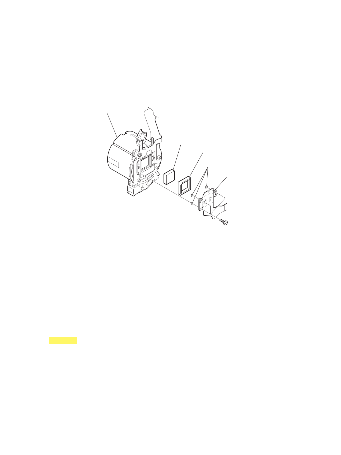
Fig. 3-11 OPTICAL UNIT, FINDER UNIT
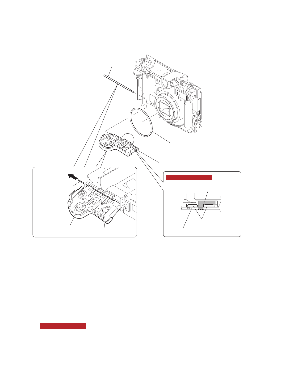
2.9 OPTICAL UNIT, FINDER UNIT
(1) OPTICAL UNIT
1. Remove the four screws.
2. While taking care of flexible printed wired board, remove the OPTICAL UNIT in the direction of arrow.
(2) FINDER UNIT
1. Remove the flexible printed wired board.
2. Remove the two screws.
3. Remove the FINDER UNIT in the direction of arrow.
3-11
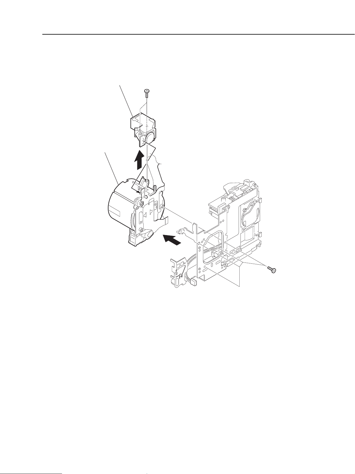
CHAPTER 3. REPAIR INSTRUCTION
OPTICAL UNIT
(1)-3
IR FILTER
(1)-3
CCD RUBBER
(1)-2
CCD WASHER
CCD UNIT
(1)-2
2.10 CCD UNIT
(1) CCD UNIT
1. Remove the three screws.
∗ Use the HAND DRILL BIT (CY9-1548-000).
2. Remove the CCD UNIT.
CAUTION
Be careful not to drop the washers.
3. Remove the CCD RUBBER, IR FILTER.
f
(1)-1
Fig. 3-12 CCD UNIT
3-12
RLS PCB ASS’Y
Claw
(2)-1
Remove soldering
(2)-2
CHAPTER 3. REPAIR INSTRUCTION
(3)-1
LITHIUM BATTERY
(3)-1
LITHIUM BATTERY HOLDER
(1)-2
(1)-1
e
BATTERY BOX UNIT
MAIN FRAME
Fig. 3-13 BATTERY BOX UNIT, RLS PCB ASS’Y, LITHIUM BATTERY HOLDER
2.11 BATTERY BOX UNIT, RLS PCB ASS’Y,
LITHIUM BATTERY HOLDER
(1) BATTERY BOX UNIT
1. Remove the two screws.
2. Remove the BATTERY BOX UNIT in the direction of arrow.
(2) RLS PCB ASS’Y
1. Remove soldering. ( : red, : black)
2. Release the claws and remove the RLS PCB ASS’Y in the direction of arrow.
(3) LITHIUM BATTERY HOLDER
1. Remove the LITHIUM BATTERY from the LITHIUM BATTERY HOLDER.
3-13
CHAPTER 3. REPAIR INSTRUCTION
Insert tweezers
or the like.
LENS PLATE
LENS BARREL
CAP
(1)-3
(1)-4
(1)-7
(1)-6
BARRIER
OPEN
SPRING
(1)-10
(1)-1
(1)-5
Insert tweezers
or the like.
(1)-3
(1)-8
(1)-6
g
(1)-9
BARRIER BASE
BARRIER DRIVE
RING
(1)-11
BARRIER
OPEN
SPRING
(1)-10
(1)-5
(1)-4
(1)-7
(1)-2
NOTE (Assembling)
BARRIER PLATE 2 SPRING
BARRIER CLOSE
SPRING
BARRIER PLATE 1
NOTE (Assembling)
(1)-3 to (1)-7
BARRIER PLATE 2
BARRIER PLATE 2
(1)-10
BARRIER PLATE 1
BARRIER
CLOSE
SPRING
BARRIER PLATE 2
SPRING
(1)-8
DC2.5V
DC2.5V
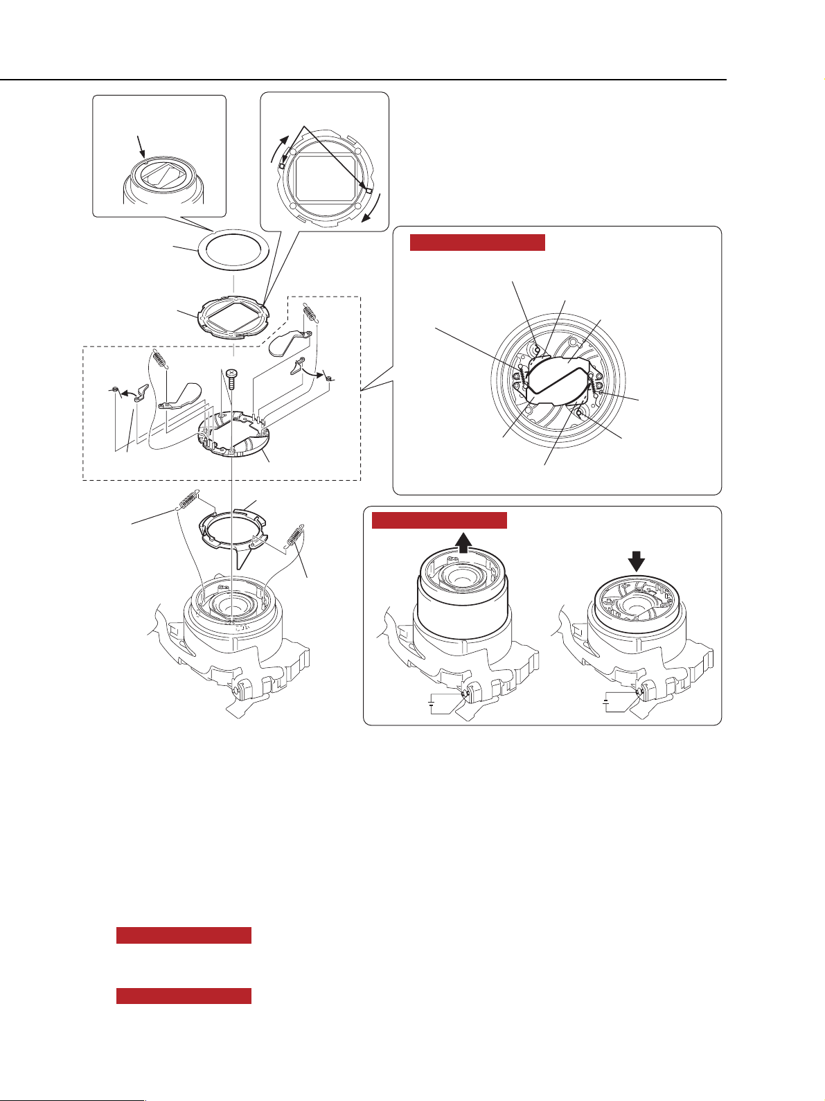
Fig. 3-14 OPTICAL UNIT
2.12 OPTICAL UNIT
(1) OPTICAL UNIT
1. Remove the LENS PLATE by inserting tweezers or the like into its groove.
2. Insert tweezers or the like to the LENS BARREL CAP. Rotate it in the clockwise direction and remove it.
3. Remove the BARRIER CLOSE SPRING (2 pieces).
4. Remove an end of the BARRIER PLATE 2 SPIRNG (2 pieces) and loosen the fastening of the BARRIER
PLATE 2.
5. Remove the BARRIER PLATE 1 (2 pieces).
6. Remove the BARRIER PLATE 2 (2 pieces).
7. Remove the BARRIER PLATE 2 SPIRNG (2 pieces).
8. Remove the two screws.
NOTE (Assembling)
9. Remove the BARRIER BASE.
10. Remove the BARRIER OPEN SPRING (2 pieces).
NOTE (Assembling)
11. Remove the BARRIER DRIVE RING.
Apply the voltage (DC 2.5V) across the motor terminal to drive the motor until the
motor stops and the BARREL is fully comes out.
Apply the voltage (DC 2.5V) across the motor terminal to drive the motor until the
motor stops and the BARREL is full housed.
3-14
CHAPTER 3. REPAIR INSTRUCTION
FINDER UNIT
(1)-2
e
(1)-1
DC2.5V
(1)-1
The SLIDER must have been moved
fully to the top of the BARREL.
BARREL
(1)-2
SLIDER
(1)-3
FINDER UNIT
DC2.5V
(1)-3
Fig. 3-15 Assembling the FINDER UNIT
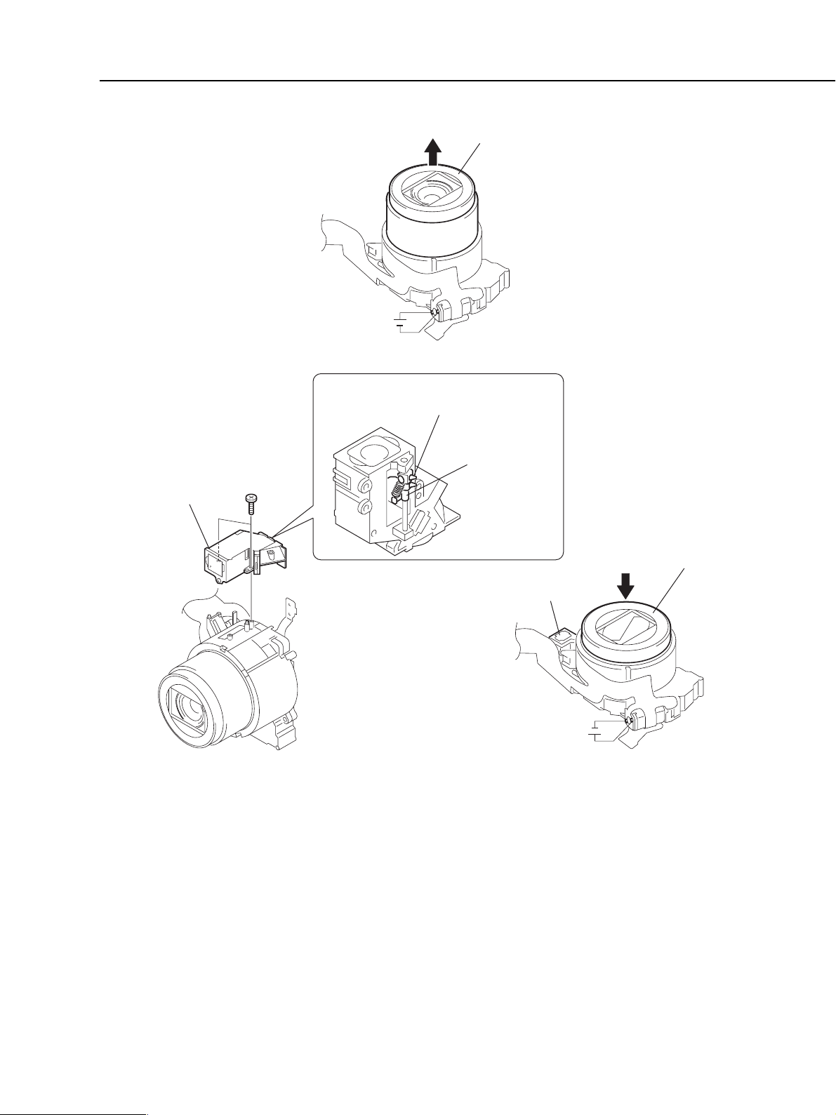
2.13 Assembling the FINDER UNIT
(1) Assembling the FINDER UNIT
1. Apply the voltage (DC 2.5V) across the motor terminal to drive the motor until the motor stops and the
BARREL fully comes out.
2. Move the SLIDER fully to the top of the BARREL and secure it with the two screws.
3. Apply the voltage (DC 2.5V) across the motor terminal to drive the motor until the motor stops and the
BARREL is full housed.
BARREL
3-15
 Loading...