

Page 1

Contents
Safety Information.............................................................................................................................2
Specifications ................................................................................................................................ 3-4
Electrostatic Discharge Sensitive (ESDS) Device Handling .........................................................5
Warranty .............................................................................................................................................5
Part List Notes ................................................................................................................................... 5
Packaging Part List, PS1 Power Stand ...........................................................................................6
Figure 1. PS1 Power Stand Packaging View ......................................................................................7
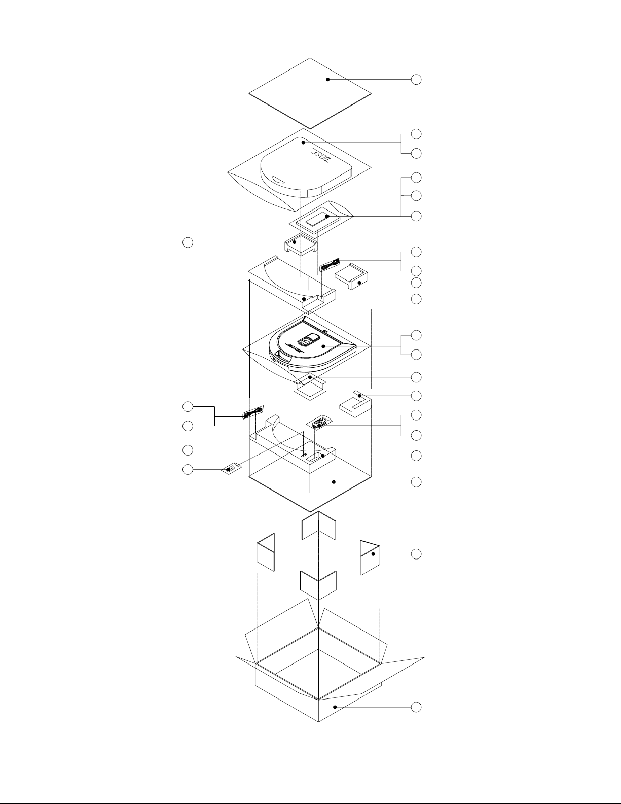
Packaging Part List, L1 Line Array ..................................................................................................8
Figure 2. L1 Line Array Packaging View .............................................................................................8
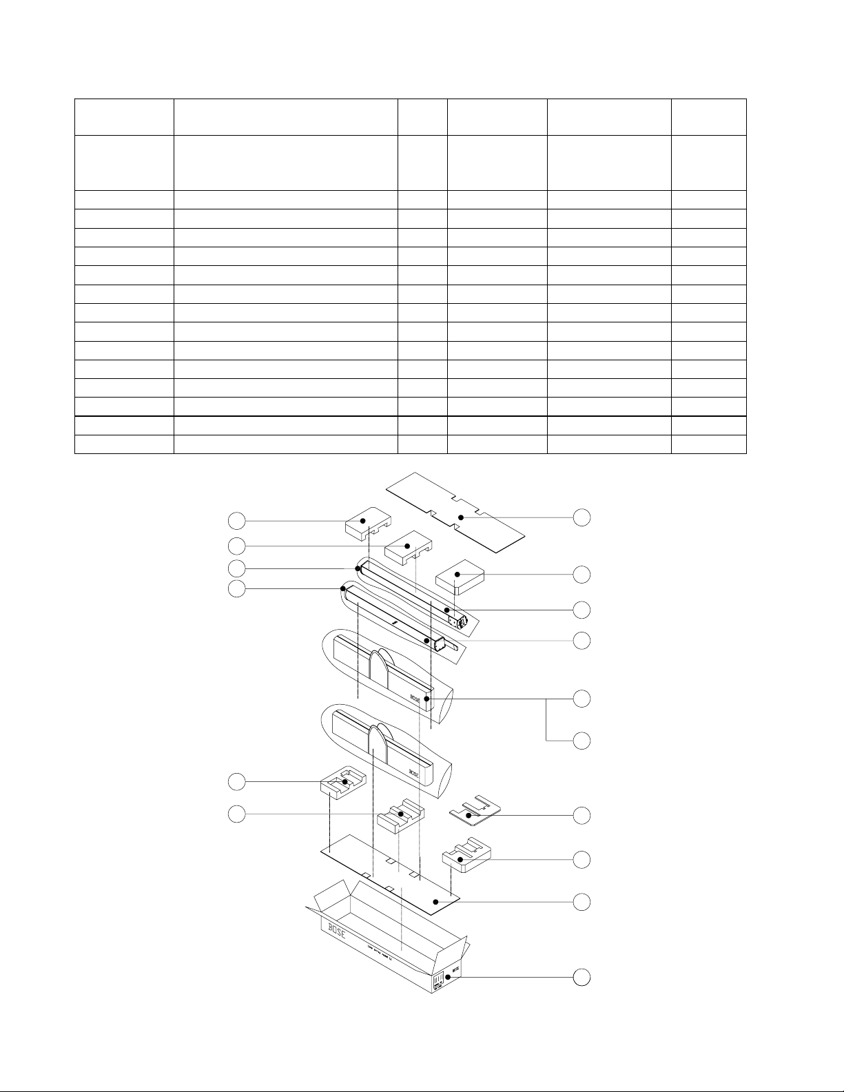
Packaging Part List, B1 Bass Module .............................................................................................9
Figure 3. B1 Bass Module Packaging View ........................................................................................9
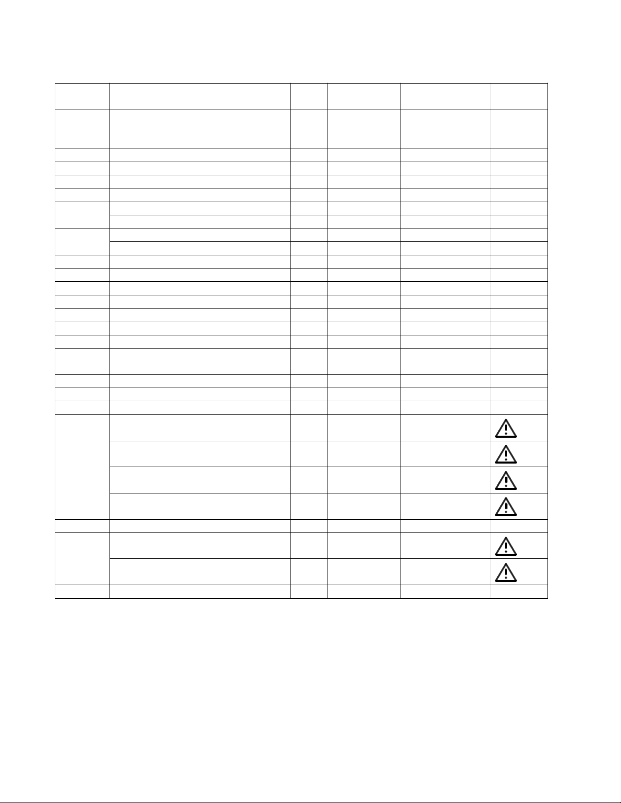
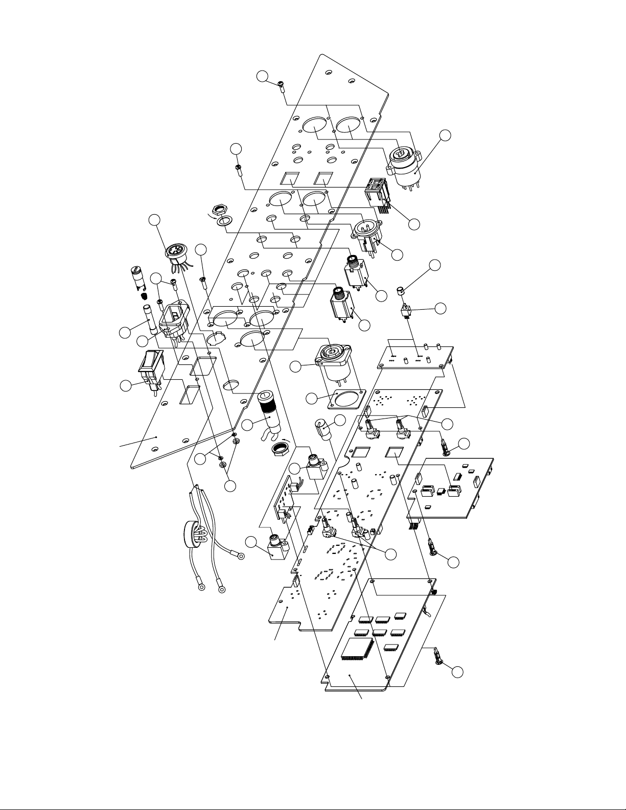
Main Part List, PS1 Power Stand ................................................................................................... 10
Figure 4. Power Stand Exploded View ..............................................................................................11
Main Part List, PS1 Power Box ......................................................................................................12
Figure 5. Power Box Exploded View .................................................................................................12
Main Part List, PS1 Input Panel Assembly ................................................................................... 13
Figure 6. Input Panel Assembly Exploded View ................................................................................14
Main Part List, LS1 Upper and Lower Line Source Arrays..........................................................15
Figure 7. Line Array Exploded View ..................................................................................................16
Main Part List, Bass Module Exploded View ................................................................................ 17
Figure 8. Bass Module Exploded View .............................................................................................17
Electrical Part Lists ................................................................................................................... 18-76
Input Panel PCB Assembly ...................................................................................................... 18-27
Digital Signal Processor (DSP) PCB Assembly ...................................................................... 28-41
Microprocessor (MCU) PCB Assembly ................................................................................... 42-45
Amplifier PCB Assembly .......................................................................................................... 46-56
27 Volt Power Supply PCB Assembly ..................................................................................... 57-66
Auxiliary Power Supply PCB Assembly .................................................................................. 67-71
EMI PCB Assembly ................................................................................................................... 72-75
Remote Control PCB Assembly .....................................................................................................76
Figure 9. PS1 Power Stand Electronics Module with Top Cover Removed ......................................77
Disassembly Procedures ...............................................................................................................78
Power Stand Procedures................................................................................................................78
Line Array Procedures ....................................................................................................................83
Bass Module Procedures ...............................................................................................................84
Figure 10. PS1 Power Stand Block Diagram ....................................................................................85
Test Procedures ........................................................................................................................ 86-92
Schematic Diagrams ............................................................................................................... 93-126
Appendix ................................................................................................................................ 127-130
Test Cables ............................................................................................................................ 127-129
Figure 11. Amplifier Output Test Cable Wiring Diagram .................................................................127
PS1 Power Stand Software Update Procedure .......................................................................... 130
Service Manual Revision History.................................................................................................131
1
Page 2

Safety Information
1. Parts that have special safety characteristics are identified by the symbol on schematics
or by special notes on the parts list. Use only replacement parts that have critical characteristics
recommended by the manufacturer.
2. Make leakage current or resistance measurements to determine that exposed parts are
acceptably insulated from the supply circuit before returning the unit to the customer.
Use the following checks to perform these measurements:
A. Leakage Current Hot Check-With the unit completely reassembled, plug the AC line cord
directly into a 120V AC outlet. (Do not use an isolation transformer during this test.) Use a
leakage current tester or a metering system that complies with American National Standards
Institute (ANSI) C101.1 "Leakage Current for Appliances" and Underwriters Laboratories (UL)
6500 / IEC 60056 paragraph 9.1.1. With the unit AC switch first in the ON position and then in
OFF position, measure from a known earth ground (metal waterpipe, conduit, etc.) to all exposed metal parts of the unit (antennas, handle bracket, metal cabinet, screwheads, metallic
overlays, control shafts, etc.), especially any exposed metal parts that offer an electrical return
path to the chassis. Any current measured must not exceed 0.5 milliamp. Reverse the unit
power cord plug in the outlet and repeat test. ANY MEASUREMENTS NOT WITHIN THE
LIMITS SPECIFIED HEREIN INDICATE A POTENTIAL SHOCK HAZARD THAT MUST BE
ELIMINATED BEFORE RETURNING THE UNIT TO THE CUSTOMER.
B. Insulation Resistance Test Cold Check-(1) Unplug the power supply and connect a jumper
wire between the two prongs of the plug. (2) Turn on the power switch of the unit. (3) Measure
the resistance with an ohmmeter between the jumpered AC plug and each exposed metallic
cabinet part on the unit. When testing 3 wire products, the resistance measured to the product
enclosure should be between 2 and infinite MOhms. Also, the resistance measured to exposed
input/output connectors should be between 4 and infinite MOhms. When testing 2 wire products, the resistance measured to exposed input/output connectors should be between 4 and
infinite MOhms. If it is not within the limits specified, there is the possibility of a shock hazard,
and the unit must be repaired and rechecked before it is returned to the customer.
CAUTION: The Bose® Personalized Amplification SystemTM contains
no user-serviceable parts. To prevent warranty infractions,
refer servicing to warranty service stations or factory service.
PROPRIETARY INFORMATION
THIS DOCUMENT CONTAINS PROPRIETARY INFORMATION OF
BOSE CORPORATION WHICH IS BEING FURNISHED ONLY FOR
THE PURPOSE OF SERVICING THE IDENTIFIED BOSE PRODUCT
BY AN AUTHORIZED BOSE SERVICE CENTER OR OWNER OF
THE BOSE PRODUCT, AND SHALL NOT BE REPRODUCED OR
USED FOR ANY OTHER PURPOSE.
2
Page 3

Specifications
MECHANICAL
External Dimensions
L1 Cylindrical Radiator: Height:86.0 in (2184 mm)
Width: 3.5 in (89 mm)
Depth: 4.0 in (105 mm)
PS1 Power Stand: Height: 5.0 in (127 mm)
Width: 26.0 in (660 mm)
Depth: 26.0 in (660 mm)
B1 Bass Module: Height: 15.3 in (380 mm)
Width: 10.3 in (257 mm)
Depth: 18.0 in (457 mm)
R1 Remote: Height:1.6 in (40 mm)
Width: 2.8 in (71 mm)
Depth: 5.6 in (141 mm)
Weight
L1 Cylindrical Radiator: 14.5 lbs (6 kg) Upper
16.0 lbs (7 kg) Lower
PS1 Power Stand: 35 lbs (16 kg)
B1 Bass Module: 28 lbs (13 kg)
R1 Remote: 0.6 lbs (0.27 kg)
Transducer Complement
L1 Cylindrical Radiator: 12 x 2.25 in (57 mm) Drivers - 4 ohms
B1 Bass Module: 2 x 5.25 in (133 mm) Drivers - 8 ohms
ACOUSTICAL
Frequency Response
L1 Cylindrical Radiator: 120 Hz to 15 kHz
B1 Bass Module: 40 Hz to 250 Hz
PAS System (with system EQ): 40 Hz to 15 kHz
Port Tuning
L1 Cylindrical Radiator: 114 Hz
B1 Bass Module: 44 Hz
3
Page 4

Specifications
ELECTRICAL
Impedance
L1 Cylindrical Radiator: 4 ohms nominal
B1 Bass module: 8 ohms nominal
System Power Handling
(Continuous full power per IEC-268-5 for duration of 100 hours)
L1 Cylindrical Radiator: 250 W (each section)
B1 Bass module: 125 W
PS1 Power Stand
Rated Power: 3 x 250 W/Ch/4 ohm. (all channels operating)
Efficiency: 80% minimum
THD at Rated Power: 1.0% Max @ 30 Hz - 15 KHz @ 4 ohms/Ch.
THD at -3dB (~125W): 0.25% Max @ 30 Hz - 15 KHz @ 4 ohms/Ch.
S/N ratio: -80dB minimum, referenced to full power
Frequency Response: 40 Hz-15 KHz +/-3 dB @ R load = 4-16 ohms
Thermal: Operate 3Ch. x 83 W Continuous @ 4 ohms,
50°C ambient with No Shut-Down
Operating AC Input Voltage: 120V Range, Approx. 80-136 VAC, Full Load
Protected against short circuited load and AC
line fluctuations of +20% and –25%
Max Power Draw: 1400 watts 50/60 Hz
Peak In Rush Current: 32 A @ 120V, 60 Hz
Power Supply Voltages: Channels 1,2,3 SMPS 27.5 VDC +/-2%
Auxiliary supply #1 +5 VDC/1 A +/- 3%
Auxiliary supply #2 +3.3 VDC/1.5 A +/- 3%
Auxiliary supply #3 +/-15 VDC/1.5 A +/- 3%
Fan 1.2.3.4 Voltage: +24 VDC +/-1V
4
Page 5

PS1 Power Stand Version 1.0 and 1.1 Differences
The PS1 power stand currently has two versions, Version 1.0 and Version 1.1, referred to in this
manual as V1.0 and V1.1. Version 1.0 was built in a US/Canada version only until June 2005.
Version 1.1 units were built in both US and non-US versions, starting in June 2005. The Version
1.1 units have a “V1.1” designation on the product label on the bottom of the power stand. The
Version 1.0 units do not have this designation.
The circuit board assemblies used in both versions of the power stand are not compatible with
each other. You cannot use a V1.0 board in a V1.1 power stand, and vice-versa. Both units act
the same from the perspective of the end customer, meaning that all input and output connections are the same and that it is the same operationally. The biggest difference between these
units is that the V1.1 units have significantly improved EMI performance. This improved performance required changes in the boards that made them incompatible with the V1.0 power stand.
Electrostatic Discharge Sensitive (ESDS)
Device Handling
This unit contains ESDS devices. We recommend the following precautions when repairing,
replacing or transporting ESDS devices:
• Perform work at an electrically grounded work station.
• Wear wrist straps that connect to the station or heel straps that connect to conductive
floor mats.
• Avoid touching the leads or contacts of ESDS devices or PC boards even if properly
grounded. Handle boards by the edges only.
• Transport or store ESDS devices in ESD protective bags, bins, or totes. Do not insert
unprotected devices into materials such as plastic, polystyrene foam, clear plastic bags,
bubble wrap or plastic trays.
Warranty
®
The Bose
able warranty. The line array and the bass module are covered by a 5-year limited warranty.
Personalized Amplification SystemTM electronics are covered by a limited 1-year transfer-
Part List Notes
1. This part is not normally available from Customer Service. Approval from the Field Service
Manager is required before ordering.
2. The individual parts located on the PCBs are listed in the Electrical Part List.
3. This part is critical for safety purposes. Failure to use a substitute replacement with the
same safety characteristics as the recommended replacement part might create shock, fire
and/or other hazards.
4. This part is referenced for informational purposes only. It is not stocked as a repair part. Refer
to the next higher assembly for a replacement part.
5
Page 6
Packaging Part List
Item
Description Qty. Bose® Part
Vendor Part
Note
PS1 Power Stand (see Figure 1)
Number
- Carton Kit, Includes Carton,
Cardboard A & B, and Packing
PE Foams 1 – 4.
1 Packing Cardboard A 2 275437 1450-7370-0
2 Carry Bag for Power Stand 1 275468 8901-4920-0
3 Poly Bag for Carry Bag 1 - 1497-7572-0
4 Poly Bag for Owner’s Manual 1 - 1497-1062-0
5 Owner’s Manual, 1 Language 1 263976 4301-7108-0 US/Can
Owner’s Manual, 8 Language 1 277296 - Euro/Aus
6 Quickstart Guide, US/Canada 1 263975 4301-7109-0
Quickstart Guide, Europe 1 278815 -
7 Poly Bag, 10”x12” 3 - 1497-4102-0
8 7-Pin MIDI Cable 1 035403 7012-6504+1
9 Packing PE Foam 4 2 275442 1493-0421-0
10 Packing PE Foam 2 1 275440 1493-0401-0
11 PS1 Power Stand Assembly 1 - REF
12 Poly Bag for Power Stand 1 - 1497-7572-0
13 Packing PE Foam 3 2 275441 1493-0411-0
14 R1 Remote Control Assembly
15 Packing PE Foam 1 1 275439 1493-0391-0
16 Packing Cardboard B 4 275438 1450-7410-0
17 Carton 1 275846 1436-4301-0-3
18 AC Line Cord, 120V, 15A,
AC Line Cord, 230V, 15A,
AC Line Cord, 230V, 15A,
AC Line Cord, 230V, 15A,
19 Poly Bag for Fuse 1 - 1497-0332-0
20 Fuse, T15A, 125V/250V,
Fuse, T10A, 125V/250V,
- Owner’s Manual, CD, 8 Language 1 279081 - Euro/Aus
w/packaging
US/Canada
Europe
Australia
UK
6.3x32mm, US/Canada
6.3x32mm, Europe
1 264029 -
1 035394 SVC-
1 273790 7010-9640-0 3
1 283048 - 3
1 284241-006 - 3
1 283624 - 3
1 273827 5120-0023-0 3
1 279425 - 3
Number
Number
PS111+REM
6
Page 7
1
2
3
4
5
6
9
7
18
19
20
7
8
9
10
11
12
13
13
7
14
15
1
16
17
Figure 1. PS1 Power Stand Packaging View
7
4x
Page 8
Packaging Part List
L1 Line Array (see Figure 2)
Item
Number
- Carton Kit, Includes Cardboard
Description Qty. Bose® Part
Number
1 263994 -
Vendor Part
Number
A and B, and Packing PE
Foams 1 - 5
1 Packing PE Foam 4 1 275462 1493-0461-0
2 Packing PE Foam 2 2 275460 1493-0441-0
3 Poly Bag 2 - 1497-7562-0 4
4 Packing PE Foam 1 1 275459 1493-0431-0
5 Packing Cardboard A 2 275457 1450-7380-0
6 Packing PE Foam 5 1 275463 1493-0471-0
7 Line Source Lower Assembly 1 REF -
8 Line Source Upper Assembly 1 REF -
9 Line Source Carry Bag 2 275470 -
10 Poly Bag for Carry Bag 2 - - 4
11 Packing Cardboard B 1 275458 1450-7400-0
12 Packing PE Foam 3 1 275461 1493-0451-0
13 Carton, no fillers 1 275848 1436-3801-0-3
- Declaration of Conformity 1 278823 - Euro
Note
1
2
3
3
4
2
5
6
7
8
9
10
11
12
5
Figure 2. L1 Line Array Packaging View
8
13
Page 9
Packaging Part List
B1 Bass Module (see Figure 3)
Item
Number
- Carton Kit – Includes All Fillers 1 263994 -
1 Carton Filler, PE Foam 2 275464 145A-7570-0
2
3
4 Bass Module Carton, No Fillers 1 275849 145B-0170-0
5
6
7
8
-
Poly Bag, 12x16x49”
B1 Bass Module
Bubble Bag for Cable
4-Wire Speakon Cable Assembly
Poly Bag for Instruction Manual
Owner's Manual, US/Canada
Owner's Manual, 8 Language
Carry Bag for Bass Module
Description Qty. Bose® Part
Number
1 - 1497-4552-0
1 032494 -
1 - 1497-1122-0
1 273826 7012-6620-2
1 - 1497-1062-0
1 272383 4301-5241-0 US/Can
1 280183 - Euro
1 276904 -
Vendor Part
Number
5
2x
6
7
8
1
Note
2
3
4
Figure 3. B1 Bass Module Packaging View
9
Page 10
Main Part List
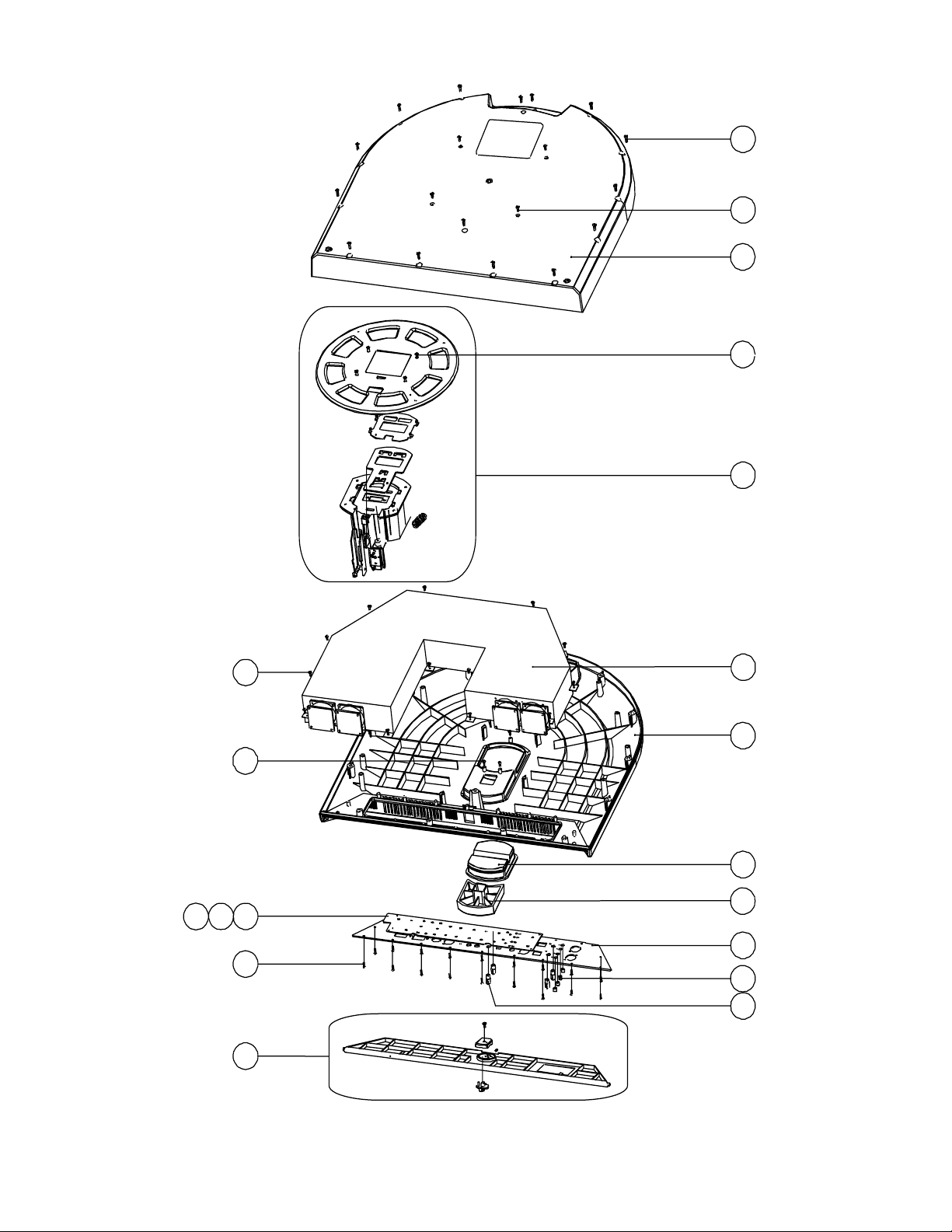
PS1 Power Stand (see Figure 4)
Item
Number
1 Screw, Mach, M4x14, Blk, Zinc 276999 2904-4014-3000 19
2 Screw, Mach, M4x8, Blk, Zinc 276997 2904-4008-3000 4
3 Housing, Lower, PS1 264035 1466-4901-0 1
4 Power Stand Cavity Assembly,
consists of:
Plate, Base, Power Stand - 1404-9601-0 1 4
PS1 Slide Spring - 2510-3611-0 1 4
Screw, Flat-CS, M2.6x8, BZ - 2901-2608-3001 4 4
Screw, Mach, M6x35mm, Blk, Zinc,
Slide Block
Screw, Mach, M4x8 276997 2904-4008-3000 2 4
Cavity, Aluminum, Power Stand - 4135-3731-0 1 4
Guide, Cavity, Power Stand - 4135-3741-0 1 4
Latch, Power Stand - 4135-3751-0 1 4
Slide, Power Stand - 4135-3761-0 1 4
Plate, Latch, Power Stand - 4135-3771-0 1 4
Post, Copper, Power Stand - 4135-3971-0 1 4
Pedal, Foot, Power stand - 4154-6921-0 1 4
Screw, Mach, M4x14, Blk, Zinc 276999 2904-4014-3000 4
Screw, Mach, M3x8, Blk, Latch Plate 277001 2901-3008-3000 4
Gasket, EVA, 5x500mm - 4153-3331-0 2 4
5 Power Box Assembly, includes PCBs
US/Canada, 120V (version 1.0 only)
US/Canada, 120V (version 1.1 only)
Euro, UK, Aus, 230V (version 1.1)
6 Screw, Mach, M3x10, Blk, Zinc 277005 2900-3010-3030 16
7 Housing, Upper, PS1 264034 1466-4801-0 1
8 Power Stand Protective Plug 273828 4154-7251-0 1
9 Power Stand Foot Pedal 264039 4154-6921-0 1
10 PS1 DSP PCB Assembly,
US/Canada, 120V (version 1.0)
US/Canada, 120V (version 1.1 only)
and Euro, UK, Aus, 230V (vers. 1.1)
11 PS1 MCU PCB Assembly,
US/Canada, 120V (version 1.0 only)
US/Canada, 120V (version 1.1 only)
and Euro, UK, Aus, 230V (vers. 1.1)
12 PS1 Input PCB Assembly,
US/Canada, 120V (version 1.0 only)
US/Canada, 120V (version 1.1 only)
and Euro, UK, Aus, 230V (vers. 1.1)
13 Input Panel Assembly, includes DSP,
MCU and Input PCBs
US/Canada, 120V (version 1.0 only)
US/Canada, 120V (version 1.1 only)
Euro, UK, Aus, 230V (vers. 1.1)
14 Power Stand Push Button 263979 2446-4901-0 4
15 Screw, Mach, M3x10, Input Panel 277004 2911-3010-3000 18
16 Power Stand V/R Knob 263986 2446-5501-0 4
17 Power Stand Door Assy, includes: 273727 - 1
Cover, I/O, Power Stand - 1466-5001-0 1 4
Knob, I/O Cover - 2446-6001-0 1 4
Latch, I/O Cover - 4154-6931-0 1 4
Latch Spring, I/O Cover - 2510-3531-0 1 4
Screw, M3x10, TTB, FH, BZ-PCB 277004 2911-3010-3000 1
- Power Stand Cavity Harness Assy 278849 - 1
Description Bose®
Part
Number
273728 - 1
276996 2903-6035-3000 1
277006
283373
283372
273730
283364
273732
283367
273731
283366
277008
283375
283374
10
Vendor
Part Number
SVC-BS060C-SMDA
-
-
PCB-BS060C-DSP
-
PCB-BS060C-MCU
-
PCB-BS060C-INP1
-
-
-
-
Qty Note
1 1
1 2
1 2
1 2
1 1
Page 11
15x
1
4x
2
3
4x
1
4
14x
3x
1110
18x
6
6
12
15
17
5
7
8
9
13
14
16
4x
4x
Figure 4. Power Stand Exploded View
11
Page 12
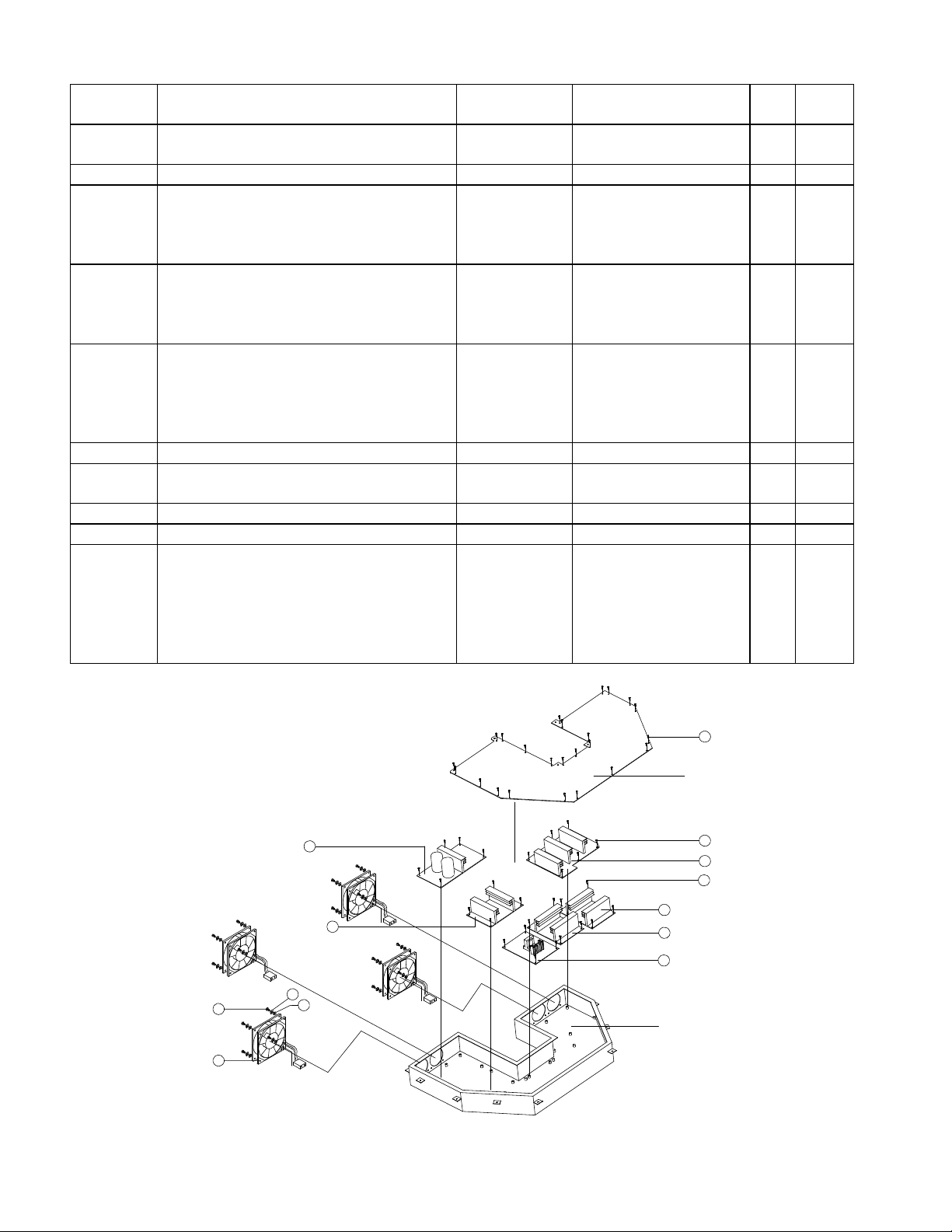
Main Part List
Item
Description Bose® Part
Vendor Part
Qty Note
PS1 Power Box (see Figure 5)
Number
1 Screw, Mach, M3x6mm, Blk, Zinc,
Number
Number
277003 2904-3006-3000 24
Power Box Top Cover
2 Screw, Mach, M3x10mm, w/washer 275435 2900-3010-3000 27
3 PS1 D-Class Amp PCB Assembly
US/Canada, 120V (version 1.0 only)
US/Canada, 120V (version 1.1 only)
273729
283363
PCB-BS060C-DAMP
-
and Euro, UK, Aus, 230V (vers. 1.1)
4 PS1 SMPS PCB Assembly
US/Canada, 120V (version 1.0 only)
US/Canada, 120V (version 1.1 only)
273734
283371
PCB-BS060C-SMPS
-
and Euro, UK, Aus, 230V (vers. 1.1)
5 PS1 Auxiliary Power Supply PCB
Assembly
US/Canada, 120V (version 1.0 only)
US/Canada, 120V (version 1.1 only)
274637
283368
PCB-BS060C-FCC
-
and Euro, UK, Aus, 230V (vers. 1.1)
6 Fan, 24VDC, 60x60x25mm, 80mA 279143 8913-4007-0 4 4
7 Screw, Mach, M3x30mm, Blk, Zinc,
277002 2904-3030-3000 16
Fan Mounting
8 Washer, Spring, M3x0.9x5.0mm - 2607-3009-0553 16 4
9 Washer, Metalid, 3.3, OD=8, T=0.5 - 2600-3005-0640 16 4
10 PS1 FCC Filter PCB Assembly
US/Canada, 120V (version 1.0 only)
US/Canada, 120V (version 1.1 only)
Euro, UK, Aus, 230V (version 1.1)
275436
283370 or
306285
283369 or
306288
PCB-BS060C-FCC
-
-
1 2
3 2
1 2
1 2
24x
1
Top
Cover
27x
3x
4
4
5
Chassis
2
3
2
10
4
16x
8
16x
16x
7
4x
6
9
Figure 5. Power Box Exploded View
12
Page 13
Main Part List
PS1 Input Panel Assembly (see Figure 6)
Item
Number
1 MCU PCB,
2 VR101,
3 VR103,
4 SW102,
5 - PS1 Push Button Knob 263979 2446-4901-0 4
6 J105, J106,
7 J112, J113 Phone Jack, 6.4mm, 9-Pin 275445 2113-1296-0 2
8 J117, J118,
9 - Bracket, Speakon Jack - 4135-3801-0 3 4
10 - Knob, I/O Panel - 2446-6301-0 4 4
11 J109 RCA Jack, White, 1P, GP 032-
12 J110 RCA Jack, Black, 1P, AU
13 J101, J102 Conn., Neutrik, NCJ10FI-V-0 275449 2113-3046-0 2
14 - PS1 Push Wheel, Preset Switch 275453 5200-4865-1 2
15 J103, J104 XLR Connector, Neutrik, 3PM 275448 2113-1698-0 2
16 - Fuse Holder, 15A/250VAC, R3-
17 - Screw, M3x10mm 277004 2911-3010-3000 16
18 Screw, M3x12, Csk, Blk,
19 - PS1 DIN Socket, 7-Pin 275454 2113-2013-0 1
20 Screw, AC Inlet Jack, M3x12 - 2900-3012-3000 2 4
21 -
22 - AC Inlet Jack 278847 2113-1144-0 1 3
23 - Switch, AC Power, SPST
24 - Washer, Spring,
25 - Nut, M3, Nickel - 2640-3022-0544 2 4
Reference
Designator
DSP PCB
VR102
VR104
SW104
J107, J108,
J114, J115,
J116
J119
Description Bose®
Part
Number
PCB SUPPORT, 12MM HIGH - 4152-0911-0 6 4
Pot, 5k Ohm, 5KX1 10C 275451 4751-0620-0 2
Pot, 20k Ohm, 20KAX1 275450 4751-0580-1 2
Switch, Push, PS828L, 8x8 mm,
MIC
Phone Jack, 6.4mm, 5-Pin 275447 2113-1340-0 7
Neutrik Speakon Connector,
NL4MD-V
09BWG
HQ032-09BBG
44A Type, 6.35x32mm,
US/Canada, 120V (1.0 and 1.1)
Euro, UK, Aus 230V (vers 1.1)
Speakon Connector
Fuse, US/Canada 120V units,
T15A, 125V/250V, 6.35x32mm,
(versions 1.0 & 1.1)
Fuse, Euro, UK, Aus 230V units,
T10A, 125/250V, 6.35x32mm,
(version 1.1)
US/Canada, 120V, (V1.0 & 1.1)
Euro, UK, Aus 230V (vers 1.1)
M3x0.9x5.5mm, BZ
275452 5200-3573-0-00 2
263605 2113-1336-1 3
275444 2113-1950-0 1
275443 2113-1169-1 1
278846
279426
- 2901-3012-3000 6 4
273827 5120-0023-0
279425 5120-0170-0
278848
279427
- 2607-3009-0553 2 4
Vendor Part
Number
4170-0021-0
4153-1100-0
5200-4826-0
5200-4873-0
Qty. Note
1 3
1 3
1 3
13
Page 14
17
17
13
21
22
23
Input Panel
19
20
24
18
25
16
11
14
15
5
6
4
7
8
9
10
2
1
11
3
Input/Output
PCB Assy
DSP PCB
Assy
Figure 6. Input Panel Assembly Exploded View
14
1
1
Page 15

Main Part List
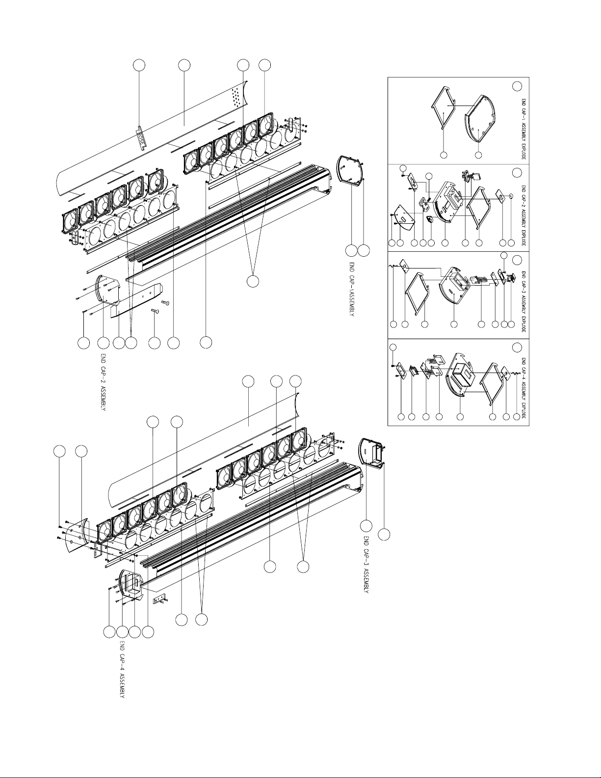
LS1 Upper and Lower Line Source Arrays (see Figure 7)
Item
Number
1 End-Cap #1 Assembly, consists of: 273753 1
End-Cap, Top, Upper, Line Source 4154-6661-0 1 4
End-Cap Gasket 4149-0491-0 1 4
2 End-Cap #2 Assembly, consists of: 273787 1
End-Cap, Bottom, Upper, Line Source 4154-6671-0 1 4
Gasket, Cap, Line Source 4149-0491-0 1 4
Airproof Sheet, End Cap, Line Source 4154-6841-0 1 4
Conn Assy, Molex, 4P, AWG#20, UL1007 7012-6615-0 1 4
Plate, Connector, 4 Pin, Floating, LS 4135-3511-0 1 4
Latch, Locking Mechanism, LS 4135-3541-0 1 4
Cover, Locking Mechanism, LS 4135-3551-0 1 4
Slide Locking Spring 1 4
Slide, Latch, Locking Mechanism, LS 4154-6631-0 1 4
3 End-Cap #3 Assembly, consists of: 273788 1
End-Cap, Top, Lower, Line Source 4154-6641-0 1 4
Gasket, Cap, Line Source 4149-0491-0 1 4
Airproof Sheet, End Cap, Line Source 4154-6841-0 1 4
Header, Vertical, Molex, 4P 2101-1438-0 1 4
Plate, Connector, 4 Pin, Fixed, LS 4135-3501-0 1 4
PCB, Molex, 10p & 4P 1725-684A-0000 1 4
Conn Assy, AWG#20, UL1015, L=150mm 7012-6616-0 1 4
4 End-Cap #4 Assembly, consists of: 273789 1
End-Cap, Bottom, Lower, Line Source 4154-6651-0 1 4
Gasket, Cap, Line Source 4149-0491-0 1 4
Airproof Sheet, End Cap, Line Source 4154-6841-0 1 4
Header, Vertical, Molex, 10P 2101-1437-0 1 4
PCB, Molex, 10p & 4P 1725-684A-0000 1 4
Plate, Connector, 10PIN, Fixed, LS 4135-3531-0 1 4
Conn Assy, AWG#20, UL1015, L=150mm 7012-6616-0 1 4
5 Screw, M3x10, Tapping 2950-3010-3000 24
6 Line Source Driver Assembly 273999 24
7 Line Source Driver Screws 96
8 Front Baffle, Upper, Assembly,
consists of:
Front Baffle-1 1404-9001-0 3 4
Baffle Gasket-1 4149-0431-0 6 4
9 Front Baffle, Lower, Assembly,
consists of:
Front Baffle-2 1404-9101-0 1 4
Baffle Gasket-1 4149-0431-0 6 4
10 Screws, Front Baffle 16
11 Grille, Lower, Assembly (w/gaskets) 263996 1
12 Nameplate, Bose Logo, Line Source 264024
13 Line Source Bayonet Assembly 264001 8901-4270-0 1
14 Line Source Bayonet Screws 2
15 Grille, Upper, Assembly (w/gaskets) 264017 4135-3571-0 1
16 Cover Plate, Lower Array 1
17 Screws, Lower Array Cover Plate 4
18 Washer, Lower Array Cover Plate 4
19 Nut, Lower Array Cover Plate 4
Description Bose®
Part
Number
273836 1
273837 1
Vendor Part
Number
Qty Note
15
Page 16
12
11
6
7
L1 Upper Array
Assembly
1234
B
K
H
M
5
1
L
G
J
F
I
A
C
E
D
B
K
8
Q
S
D
13
2
5
14
8
10
7
10
L1 Lower Array
Assembly
15
6
7
6
K
W
V
R
B
Q
U
T
O
N
P
S
D
B
17
16
3
5
10
10
19
18
4
5
9
8
Figure 7. Line Array Exploded View
16
Page 17
Main Part List
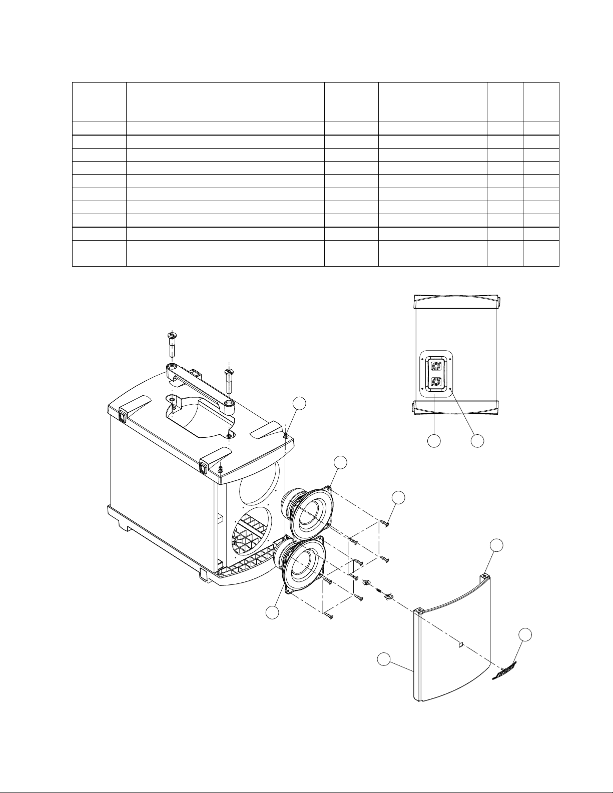
Bass Module Exploded View (see Figure 8)
Item
Number
1 Screw, M4 X 28, BK, B1 Grille 275465 2908-4028-3400 4
2 Woofer Assembly 263998 2
3 Gasket, Woofer Assembly 263998 2
4 Screw, M4 X 16, BK, B1 Driver 275466 2913-4016-3000 8
5 Grille Assembly 263992 1
6 Gasket, Grille Assembly 2
7 Logo Assembly 1
8 B1 Terminal Panel Assembly 276409 1
9 Screw, M3 X 12, BK, B1 Input Cup 275467 2900-3012-3000 4
- 4-Wire Speakon to Speakon Cable
Assembly, L=1.5M
Description
Number
Bose
273826 7012-6620-1 1
Part
Vendor Part
Number
Qty Note
124x
8
2x
48x
32x
62x
9
5
7
Figure 8. Bass Module Exploded View
17
Page 18

Electrical Part List
Input Panel PCB Assembly
Resistors
Reference
Designator
R101 10M, 0805, 1/10W, 1% 4720-106A-J 4
R102 1M, 0805, 1/10W, 1% 4720-105A-J 4
R103 51 ohm, 0805, 1/10W, 1% 4720-510A-J 4
R104 1K, 0805, 1/10W, 1% 4720-102A-J 4
R105 15K, 0805, 1/10W, 1% 4720-153A-J 4
R106 51 ohm, 0805, 1/10W, 1% 4720-510A-J 4
R107 15K, 0805, 1/10W, 1% 4720-153A-J 4
R108 15K, 0805, 1/10W, 1% 4720-153A-J 4
R109 10K, 0805, 1/10W, 1% 4720-103J-J 4
R110 22K, 0805, 1/10W, 5% 4720-223J-J 4
R111 5.6K, 0805, 1/10W, 5% 4720-562J-J 4
R112 1M, 0805, 1/10W, 1% 4720-105J-J 4
R113 10K, 0805, 1/10W, 5% 4720-103J-J 4
R114 22K, 0805, 1/10W, 5% 4720-223J-J 4
R115 5.6K, 0805, 1/10W, 5% 4720-562J-J 4
R116 1M, 0805, 1/10W, 1% 4720-105J-J 4
R117 100 ohm, 0805, 1/10W, 5% 4720-101J-J 4
R118 10K, 0805, 1/10W, 1% (Version 1.0 units) 4720-103A-J 4
R118 33K, 0805, 1/10W, 1% (Version 1.1 units) 4720-333A-J 4
R119 10K, 0805, 1/10W, 1% 4720-103A-J 4
R120 220 ohm, 0805, 1/10W, 5% 4720-221J-J 4
R121 10K, 0805, 1/10W, 1% 4720-103A-J 4
R123 10K, 0805, 1/10W, 1% 4720-103A-J 4
R124 220 ohm, 0805, 1/10W, 5% 4720-221J-J 4
R125 1.2K, 0805, 1/10W, 5% 4720-122J-J 4
R126 1.2K, 0805, 1/10W, 5% 4720-122J-J 4
R127 2K, 0805, 1/10W, 1% 4720-202A-J 4
R128 2K, 0805, 1/10W, 1% 4720-202A-J 4
R129 10 ohm, 0805, 1/10W, 5% 4720-100J-J 4
R130 10 ohm, 0805, 1/10W, 5% 4720-100J-J 4
R131 10K, 0805, 1/10W, 1% 4720-103A-J 4
R132 10K, 0805, 1/10W, 1% 4720-103A-J 4
R133 20 ohm, 0805, 1/10W, 5% 4720-200J-J 4
R134 1M, 0805, 1/10W, 1% 4720-105J-J 4
R135 10 ohm, 0805, 1/10W, 5% 4720-100J-J 4
R136 10M, 0805, 1/10W, 1% 4720-106A-J 4
R137 1M, 0805, 1/10W, 1% 4720-105A-J 4
R138 100 ohm, 0805, 1/10W, 1% 4720-101A-J 4
R139 1K, 0805, 1/10W, 1% 4720-102A-J 4
R140 10K, 0805, 1/10W, 1% 4720-103A-J 4
R141 100 ohm, 0805, 1/10W, 1% 4720-101A-J 4
R142 10K, 0805, 1/10W, 1% 4720-103A-J 4
R150 15K, 0805, 1/10W, 1% 4720-153A-J 4
R152 100 ohm, 0805, 1/10W, 5% 4720-101J-J 4
R153 10K, 0805, 1/10W, 1% (Version 1.0 units) 4720-103A-J 4
R153 33K, 0805, 1/10W, 1% (Version 1.1 units) 4720-333A-J 4
Description Vendor Part
Number
18
Note
Page 19

Electrical Part List
Input Panel PCB Assembly
Resistors (continued)
Reference
Designator
R154 10K, 0805, 1/10W, 1% 4720-103A-J 4
R155 10K, 0805, 1/10W, 1% 4720-103A-J 4
R157 10K, 0805, 1/10W, 1% 4720-103A-J 4
R158 220 ohm, 0805, 1/10W, 5% 4720-221J-J 4
R159 220 ohm, 0805, 1/10W, 5% 4720-221J-J 4
R162 2K, 0805, 1/10W, 1% 4720-202A-J 4
R163 2K, 0805, 1/10W, 1% 4720-202A-J 4
R164 10 ohm, 0805, 1/10W, 5% 4720-100J-J 4
R165 10 ohm, 0805, 1/10W, 5% 4720-100J-J 4
R166 10K, 0805, 1/10W, 1% 4720-103A-J 4
R167 10K, 0805, 1/10W, 1% 4720-103A-J 4
R168 20 ohm, 0805, 1/10W, 5% 4720-200J-J 4
R169 1M, 0805, 1/10W, 1% 4720-105J-J 4
R170 10 ohm, 0805, 1/10W, 5% 4720-100J-J 4
R171 300 ohm, 0805, 1/10W, 5% 4720-301J-J 4
R172 100 ohm, 0805, 1/10W, 1% 4720-101A-J 4
R173 12K, 0805, 1/10W, 1% 4720-123A-J 4
R174 100 ohm, 0805, 1/10W, 5% 4720-101J-J 4
R175 300 ohm, 0805, 1/10W, 5% 4720-301J-J 4
R176 100 ohm, 0805, 1/10W, 1% 4720-101A-J 4
R177 12K, 0805, 1/10W, 1% 4720-123A-J 4
R178 100 ohm, 0805, 1/10W, 5% 4720-101J-J 4
R179 220 ohm, 0805, 1/10W, 5% 4720-221J-J 4
R180 22K, 0805, 1/10W, 5% 4720-223J-J 4
R181 51K, 0805, 1/10W, 5% 4720-513J-J 4
R182 220 ohm, 0805, 1/10W, 5% 4720-221J-J 4
R183 220 ohm, 0805, 1/10W, 5% 4720-221J-J 4
R185 51K, 0805, 1/10W, 5% 4720-513J-J 4
R186 220 ohm, 0805, 1/10W, 5% 4720-221J-J 4
R187 51K, 0805, 1/10W, 5% 4720-513J-J 4
R188 150K, 0805, 1/10W, 5% 4720-154J-J 4
R189 1K, 0805, 1/10W, 5% 4720-102J-J 4
R190 1K, 0805, 1/10W, 5% 4720-102J-J 4
R191 30K, 0805, 1/10W, 5% 4720-303J-J 4
R192 2.2K, 0805, 1/10W, 5% 4720-222J-J 4
R193 3.3K, 0805, 1/10W, 5% 4720-332J-J 4
R197 51K, 0805, 1/10W, 5% 4720-513J-J 4
R198 150K, 0805, 1/10W, 5% 4720-154J-J 4
R199 1K, 0805, 1/10W, 5% 4720-102J-J 4
R200 1K, 0805, 1/10W, 5% 4720-102J-J 4
R201 30K, 0805, 1/10W, 5% 4720-303J-J 4
R202 2.2K, 0805, 1/10W, 5% 4720-222J-J 4
R204 3.3K, 0805, 1/10W, 5% 4720-332J-J 4
R207 220 ohm, 0805, 1/10W, 5% 4720-221J-J 4
R208 220 ohm, 0805, 1/10W, 5% 4720-221J-J 4
R209 100 ohm, 0805, 1/10W, 5% 4720-101J-J 4
R210 12K, 0805, 1/10W, 5% 4720-123J-J 4
Description Vendor Part
Number
19
Note
Page 20

Electrical Part List
Input Panel PCB Assembly
Resistors (continued)
Reference
Designator
R211 10 ohm, 0805, 1/10W, 5% 4720-100J-J 4
R212 100 ohm, 0805, 1/10W, 5% 4720-101J-J 4
R213 12K, 0805, 1/10W, 5% 4720-123J-J 4
R214 47K, 0805, 1/10W, 5% 4720-473J-J 4
R215 100 ohm, 0805, 1/10W, 5% 4720-101J-J 4
R216 100 ohm, 0805, 1/10W, 5% 4720-101J-J 4
R217 12K, 0805, 1/10W, 5% 4720-123J-J 4
R218 47K, 0805, 1/10W, 5% 4720-473J-J 4
R219 100 ohm, 0805, 1/10W, 5% 4720-101J-J 4
R220 100 ohm, 0805, 1/10W, 5% 4720-101J-J 4
R221 12K, 0805, 1/10W, 5% 4720-123J-J 4
R222 47K, 0805, 1/10W, 5% 4720-473J-J 4
R223 100 ohm, 0805, 1/10W, 5% 4720-101J-J 4
R224 2.7K, 0805, 1/10W, 5% 4720-272J-J 4
R225 2.7K, 0805, 1/10W, 5% 4720-272J-J 4
R226 10K, 0805, 1/10W, 1% 4720-103A-J 4
R227 10K, 0805, 1/10W, 1% 4720-103A-J 4
R229 47K, 0805, 1/10W, 5% 4720-473J-J 4
R230 47K, 0805, 1/10W, 5% 4720-473J-J 4
R231 10K, 0805, 1/10W, 1% 4720-103A-J 4
R232 10K, 0805, 1/10W, 1% 4720-103A-J 4
R234 47K, 0805, 1/10W, 5% 4720-473J-J 4
R235 47K, 0805, 1/10W, 5% 4720-473J-J 4
R238 5.6K, 0805, 1/10W, 5% 4720-562J-J 4
R239 47K, 0805, 1/10W, 5% 4720-473J-J 4
R240 47K, 0805, 1/10W, 5% 4720-473J-J 4
R241 47K, 0805, 1/10W, 5% 4720-473J-J 4
R242 22K, 0805, 1/10W, 5% 4720-223J-J 4
R243 5.6K, 0805, 1/10W, 5% 4720-562J-J 4
R244 47K, 0805, 1/10W, 5% 4720-473J-J 4
R245 100K, 0805, 1/10W, 5% 4720-104J-J 4
R246 100K, 0805, 1/10W, 5% 4720-104J-J 4
R247 100K, 0805, 1/10W, 5% 4720-104J-J 4
R248 10K, 0805, 1/10W, 1% 4720-103A-J 4
R249 10K, 0805, 1/10W, 1% 4720-103A-J 4
R250 10K, 0805, 1/10W, 1% 4720-103A-J 4
R251 10K, 0805, 1/10W, 1% 4720-103A-J 4
R252 22K, 0805, 1/10W, 5% 4720-223J-J 4
R253 560 ohm, 0805, 1/10W, 5% 4720-561J-J 4
R254 10K, 0805, 1/10W, 1% 4720-103A-J 4
R255 10K, 0805, 1/10W, 1% 4720-103A-J 4
R256 22K, 0805, 1/10W, 5% 4720-223J-J 4
R257 560 ohm, 0805, 1/10W, 5% 4720-561J-J 4
R258 100K, 0805, 1/10W, 5% 4720-104J-J 4
R259 100K, 0805, 1/10W, 5% 4720-104J-J 4
R260 100K, 0805, 1/10W, 5% 4720-104J-J 4
R261 100K, 0805, 1/10W, 5% 4720-104J-J 4
Description Vendor Part
Number
Note
20
Page 21

Electrical Part List
Input Panel PCB Assembly
Capacitors
Reference
Designator
C101 100pF, 0805, 50V, 10% 150F-101K-J-BD 4
C102 0.1uF, 0805, 50V, 10% 150F-104K-J-BD 4
C106 20pF, 0805, 50V, 5% 150F-200J-J-BD 4
C107 20pF, 0805, 50V, 5% 150F-200J-J-BD 4
C110 22uF, 63V, 20%, RL, 6.5X11 (Version 1.0 units) 157I-226M-5-LU 4
C110 22uF, 50V, 20%, RLT, 5X11 (Version 1.1 units) 157F-226M-K-IU 4
C112 22uF, 63V, 20%, RL, 6.5X11 (Version 1.0 units) 157I-226M-5-LU 4
C112 22uF, 50V, 20%, RLT, 5X11 (Version 1.1 units) 157F-226M-K-IU 4
C113 47uF, 35V, 20%, RL, 5x11 (Version 1.0 units) 157Q-476M-5-IUL 4
C113 47uF, 35V, 20%, RLT, 5x11 (Version 1.1 units) 157Q-476M-K-IUI 4
C114 47uF, 35V, 20%, RL, 5x11 (Version 1.0 units) 157Q-476M-5-IUL 4
C114 47uF, 35V, 20%, RLT, 5x11 (Version 1.1 units) 157Q-476M-K-IUI 4
C115 100pF, 0805, 50V, 10% 150F-101K-J-BD 4
C116 100pF, 0805, 50V, 10% 150F-101K-J-BD 4
C117 0.1uF, 0805, 50V, 10% 150F-104K-J-BD 4
C118 0.1uF, 0805, 50V, 10% 150F-104K-J-BD 4
C119 100pF, 0805, 50V, 10% 150F-101K-J-BD 4
C123 20pF, 0805, 50V, 5% 150F-200J-J-BD 4
C124 20pF, 0805, 50V, 5% 150F-200J-J-BD 4
C127 22uF, 63V, 20%, RL, 6.5X11 (Version 1.0 units) 157I-226M-5-LU 4
C127 22uF, 50V20%, RLT, 5X11 (Version 1.1 units) 157F-226M-K-IU 4
C129 22uF, 63V, 20%, RL, 6.5X11 (Version 1.0 units) 157I-226M-5-LU 4
C129 22uF, 50V20%, RLT, 5X11 (Version 1.1 units) 157F-226M-K-IU 4
C130 47uF, 35V, 20%, RL, 5x11 157Q-476M-5-IUL 4
C131 47uF, 35V, 20%, RL, 5x11 157Q-476M-5-IUL 4
C132 100pF, 0805, 50V, 10% 150F-101K-J-BD 4
C133 100pF, 0805, 50V, 10% 150F-101K-J-BD 4
C134 0.1uF, 0805, 50V, 10% 150F-104K-J-BD 4
C135 100pF, 0805, 50V, 10% 150F-101K-J-BD 4
C136 10uF, 25V, 20%, RL, 5x11 (Version 1.0 units) 157E-106M-5-IU 4
C136 10uF, 50V, 20%, RLT, 5X11 (Version 1.1 units) 157F-106M-K-IU 4
C137 1000pF, 0805, 50V, 10% 150F-102K-J-BD 4
C138 100pF, 0805, 50V, 10% 150F-101K-J-BD 4
C139 10uF, 25V, 20%, RL, 5x11 (Version 1.0 units) 157E-106M-5-IU 4
C139 10uF, 50V, 20%, RLT, 5X11 (Version 1.1 units) 157F-106M-K-IU 4
C140 1000pF, 0805, 50V, 10% 150F-102K-J-BD 4
C141 0.1uF, 0805, 50V, 10% 150F-104K-J-BD 4
C142 1000pF, 0805, 50V, 10% 150F-102K-J-BD 4
C143 2.2uF, 50V, 20%, RL, 5x11 (Version 1.0 units) 157F-225M-5-IU 4
C143 2.2uF, 50V, 20%, RLT, 5X11 (Version 1.1 units) 157F-225M-K-IU 4
C144 100pF, 0805, 50V, 10% 150F-101K-J-BD 4
C145 1000pF, 0805, 50V, 10% 150F-102K-J-BD 4
C146 2.2uF, 50V, 20%, RL, 5x11 (Version 1.0 units) 157F-225M-5-IU 4
C146 2.2uF, 50V, 20%, RLT, 5X11 (Version 1.1 units) 157F-225M-K-IU 4
C147 100pF, 0805, 50V, 10% 150F-101K-J-BD 4
C148 0.1uF, 0805, 50V, 10% 150F-104K-J-BD 4
C149 0.1uF, 0805, 50V, 10% 150F-104K-J-BD 4
Description Vendor Part
Number
21
Note
Page 22

Electrical Part List
Input Panel PCB Assembly
Capacitors (continued)
Reference
Designator
C150 0.1uF, 0805, 50V, 10% 150F-104K-J-BD 4
C151 0.1uF, 0805, 50V, 10% 150F-104K-J-BD 4
C152 0.1uF, 0805, 50V, 10% 150F-104K-J-BD 4
C153 0.1uF, 0805, 50V, 10% 150F-104K-J-BD 4
C156 0.1uF, 0805, 50V, 10% 150F-104K-J-BD 4
C157 0.1uF, 0805, 50V, 10% 150F-104K-J-BD 4
C158 0.1uF, 0805, 50V, 10% 150F-104K-J-BD 4
C159 0.1uF, 0805, 50V, 10% 150F-104K-J-BD 4
C160 0.1uF, 0805, 50V, 10% 150F-104K-J-BD 4
C161 0.1uF, 0805, 50V, 10% 150F-104K-J-BD 4
C162 0.1uF, 0805, 50V, 10% 150F-104K-J-BD 4
C163 0.1uF, 0805, 50V, 10% 150F-104K-J-BD 4
C164 0.1uF, 0805, 50V, 10% 150F-104K-J-BD 4
C165 0.1uF, 0805, 50V, 10% 150F-104K-J-BD 4
C166 47uF, 25V, 20%, RL, 5x11 (Version 1.0 units) 157E-476M-5-IU 4
C166 47uF, 50V, 20%, RLT (Version 1.1 units) 157F-476M-K-LUI 4
C167 47uF, 25V, 20%, RL, 5x11 (Version 1.0 units) 157E-476M-5-IU 4
C167 47uF, 50V, 20%, RLT (Version 1.1 units) 157F-476M-K-LUI 4
C168 1uF, 50V, 20%, RL, 4x7 157F-105M-5-GMK 4
C169 4.7uF, 50V, 20%, RL, 4X7 157F-475M-5-GMK 4
C170 220uF, 35V, 20%, RL, 8x11.5 157Q-227M-5-OV 4
C171 1uF, 50V, 20%, RL, 4x7 157F-105M-5-GMK 4
C172 4.7uF, 50V, 20%, RL, 4X7 157F-475M-5-GMK 4
C173 220uF, 35V, 20%, RL, 8x11.5 157Q-227M-5-OV 4
C174 0.1uF, 0805, 50V, 10% 150F-104K-J-BD 4
C175 0.1uF, 0805, 50V, 10% 150F-104K-J-BD 4
C176 0.1uF, 0805, 50V, 10% 150F-104K-J-BD 4
C177 0.1uF, 0805, 50V, 10% 150F-104K-J-BD 4
C178A 100uF, 35V, 20%, RL, 8X11 157Q-107M-5-OU 4
C179A 100uF, 35V, 20%, RL, 8X11 157Q-107M-5-OU 4
C182 1000pF, 0805, 50V, 10% 150F-102K-J-BD 4
C183 1000pF, 0805, 50V, 10% 150F-102K-J-BD 4
C184 1000pF, 0805, 50V, 10% 150F-102K-J-BD 4
C185 2.2uF, 50V, 20%, RL, 4x7 (Version 1.0 units) 157F-225M-5-GMK 4
C185 2.2uF, 50V, 20%, RLT, 5X11 (Version 1.1 units) 157F-225M-K-IU 4
C186 2.2uF, 50V, 20%, RL, 5x11 (Version 1.0 units) 157F-225M-5-IU 4
C186 2.2uF, 50V, 20%, RLT, 5X11 (Version 1.1 units) 157F-225M-K-IU 4
C187 1000pF, 0805, 50V, 10% 150F-102K-J-BD 4
C188 0.1uF, 0805, 50V, 10% 150F-104K-J-BD 4
C189 0.1uF, 0805, 50V, 10% 150F-104K-J-BD 4
C190 0.1uF, 0805, 50V, 10% 150F-104K-J-BD 4
C191 0.1uF, 0805, 50V, 10% 150F-104K-J-BD 4
C192 2.2uF, 50V, 20%, RL, 5x11 (Version 1.0 units) 157F-225M-5-IU 4
C192 2.2uF, 50V, 20%, RLT, 5X11 (Version 1.1 units) 157F-225M-K-IU 4
C193 1000pF, 0805, 50V, 10% 150F-102K-J-BD 4
C194 10uF, 25V, 20%, RL, 5x11 (Version 1.0 units) 157E-106M-5-IU 4
C194 10uF, 50V, 20%, RLT, 5X11 (Version 1.1 units) 157F-106M-K-IU 4
Description Vendor Part
Number
Note
22
Page 23

Electrical Part List
Input Panel PCB Assembly
Capacitors (continued)
Reference
Designator
C195 2.2uF, 50V, 20%, RL, 5x11 (Version 1.0 units) 157F-225M-5-IU 4
C195 2.2uF, 50V, 20%, RLT, 5X11 (Version 1.1 units) 157F-225M-K-IU 4
C196 1000pF, 0805, 50V, 10% 150F-102K-J-BD 4
C197 10uF, 25V, 20%, RL, 5x11 (Version 1.0 units) 157E-106M-5-IU 4
C197 10uF, 50V, 20%, RLT, 5X11 (Version 1.1 units) 157F-106M-K-IU 4
C198 2.2uF, 50V, 20%, RL, 5x11 (Version 1.0 units) 157F-225M-5-IU 4
C198 2.2uF, 50V, 20%, RLT, 5X11 (Version 1.1 units) 157F-225M-K-IU 4
C199 1000pF, 0805, 50V, 10% 150F-102K-J-BD 4
C200 10uF, 25V, 20%, RL, 4X7 (Version 1.0 units) 157E-106M-5-GM 4
C200 10uF, 50V, 20%, RLT, 5X11 (Version 1.1 units) 157F-106M-K-IU 4
C201 1000pF, 0805, 50V, 10% 150F-102K-J-BD 4
C202 1000pF, 0805, 50V, 10% 150F-102K-J-BD 4
C203 1000pF, 0805, 50V, 10% 150F-102K-J-BD 4
C204 1000pF, 0805, 50V, 10% 150F-102K-J-BD 4
C211 1000pF, 0805, 50V, 10% 150F-102K-J-BD 4
C212 1000pF, 0805, 50V, 10% 150F-102K-J-BD 4
C213 1000pF, 0805, 50V, 10% 150F-102K-J-BD 4
C214 1000pF, 0805, 50V, 10% 150F-102K-J-BD 4
C215 1000pF, 0805, 50V, 10% 150F-102K-J-BD 4
C216 1000pF, 0805, 50V, 10% 150F-102K-J-BD 4
C217 1000pF, 0805, 50V, 10% 150F-102K-J-BD 4
C218 1000pF, 0805, 50V, 10% 150F-102K-J-BD 4
C221 1000pF, 0805, 50V, 10% 150F-102K-J-BD 4
C223 1000pF, 0805, 50V, 10% 150F-102K-J-BD 4
C225 1000pF, 0805, 50V, 10% 150F-102K-J-BD 4
C227 1000pF, 0805, 50V, 10% 150F-102K-J-BD 4
C230 100pF, 0805, 50V, 10% 150F-101K-J-BD 4
C232 10uF, 25V, 20%, RL, 5x11 (Version 1.0 units) 157E-106M-5-IU 4
C232 10uF, 50V, 20%, RLT, 5X11 (Version 1.1 units) 157F-106M-K-IU 4
C233 10uF, 25V, 20%, RL, 5x11 (Version 1.0 units) 157E-106M-5-IU 4
C233 10uF, 50V, 20%, RLT, 5X11 (Version 1.1 units) 157F-106M-K-IU 4
C234 10uF, 25V, 20%, RL, 5x11 (Version 1.0 units) 157E-106M-5-IU 4
C234 10uF, 50V, 20%, RLT, 5X11 (Version 1.1 units) 157F-106M-K-IU 4
C235 10uF, 25V, 20%, RL, 5x11 (Version 1.0 units) 157E-106M-5-IU 4
C235 10uF, 50V, 20%, RLT, 5X11 (Version 1.1 units) 157F-106M-K-IU 4
C236 1000uF, 16V, 20%, RL, 10x16 157D-108M-5-S5 4
C237 1000uF, 16V, 20%, RL, 10x16 157D-108M-5-S5 4
C238 0.1uF, 0805, 50V, 10% 150F-104K-J-BD 4
C239 0.1uF, 0805, 50V, 10% 150F-104K-J-BD 4
C240 2.2uF, 50V, 20%, RL, 4x7 (Version 1.0 units) 157F-225M-5-GMK 4
C240 2.2uF, 50V, 20%, RLT, 5X11 (Version 1.1 units) 157F-225M-K-IU 4
C240A 100pF, 0805, 50V, 10% 150F-101K-J-BD 4
C241 33pF, 0805, 50V, 5% 150F-330J-J-BD 4
C242 1000pF, 0805, 50V, 10% 150F-102K-J-BD 4
C243 20pF, 0805, 50V, 5% 150F-200J-J-BD 4
C244 20pF, 0805, 50V, 5% 150F-200J-J-BD 4
C245 2.2uF, 50V, 20%, RL, 4x7 (Version 1.0 units) 157F-225M-5-GMK 4
Description Vendor Part
Number
23
Note
Page 24
Electrical Part List
Input Panel PCB Assembly
Capacitors (continued)
Reference
Designator
C245 2.2uF, 50V, 20%, RLT, 5X11 (Version 1.1 units) 157F-225M-K-IU 4
C246 1000pF, 0805, 50V, 10% 150F-102K-J-BD 4
C247 1000pF, 0805, 50V, 10% 150F-102K-J-BD 4
C248 820pF, 0805, 50V, 10% 150F-821K-J-BD 4
C249 820pF, 0805, 50V, 10% 150F-821K-J-BD 4
Description Vendor Part
Number
Note
Diodes
Reference
Designator
D101 LL4148, SM 4804-1480-3 4
D102 LL4148, SM 4804-1480-3 4
D103 LL4148, SM 4804-1480-3 4
D104 LL4148, SM 4804-1480-3 4
D105 LL4148, SM 4804-1480-3 4
D106 LL4148, SM 4804-1480-3 4
D107 LL4148, SM 4804-1480-3 4
D108 LL4148, SM 4804-1480-3 4
D109 LL4148, SM 4804-1480-3 4
D110 LL4148, SM 4804-1480-3 4
D113 LL4148, SM 4804-1480-3 4
D114 LL4148, SM 4804-1480-3 4
D115 LL4148, SM 4804-1480-3 4
D116 LL4148, SM 4804-1480-3 4
D117 LL4148, SM 4804-1480-3 4
D118 LL4148, SM 4804-1480-3 4
D119 LL4148, SM 4804-1480-3 4
D120 LL4148, SM 4804-1480-3 4
D121 LL4148, SM 4804-1480-3 4
D122 LL4148, SM 4804-1480-3 4
D123 LL4148, SM 4804-1480-3 4
D124 LL4148, SM 4804-1480-3 4
D125 LL4148, SM 4804-1480-3 4
D126 LL4148, SM 4804-1480-3 4
D127 LL4148, SM 4804-1480-3 4
D127A LL4148, SM 4804-1480-3 4
D128 LL4148, SM 4804-1480-3 4
D128A LL4148, SM 4804-1480-3 4
D129 LL4148, SM 4804-1480-3 4
D130 LL4148, SM 4804-1480-3 4
D131 LL4148, SM 4804-1480-3 4
D132 LL4148, SM 4804-1480-3 4
D133 LL4148, SM 4804-1480-3 4
D134 LL4148, SM 4804-1480-3 4
D135 LL4148, SM 4804-1480-3 4
D136 LL4148, SM 4804-1480-3 4
Description Vendor Part
Number
Note
24
Page 25
Electrical Part List
Input Panel PCB Assembly
Diodes (continued)
Reference
Designator
D137 LL4148, SM 4804-1480-3 4
D138 LL4148, SM 4804-1480-3 4
D139 LL4148, SM 4804-1480-3 4
D140 LL4148, SM 4804-1480-3 4
D141 LL4148, SM 4804-1480-3 4
D142 LL4148, SM 4804-1480-3 4
D143 LL4148, SM 4804-1480-3 4
D144 LL4148, SM 4804-1480-3 4
Description Vendor Part
Number
Note
Zener Diodes
Reference
Designator
Z101 5.6V, 1/2W, SMD 4837-5A61-3 4
Z102 5.1V, 1/2W, SMD 4837-5A11-3 4
Z103 5.6V, 1/2W, SMD 4837-5A61-3 4
Z104 5.1V, 1/2W, SMD 4837-5A11-3 4
Z105 3.3V, 1/2W, UD23.3B, SMD, ROHM 4837-3V31-3 4
Z106 3.3V, 1/2W, UD23.3B, SMD, ROHM 4837-3V31-3 4
Z107 5.6V, 1/2W, SMD (Version 1.1 units) 4837-5A61-3 4
Z108 5.6V, 1/2W, SMD (Version 1.1 units) 4837-5A61-3 4
Z109 5.6V, 1/2W, SMD (Version 1.1 units) 4837-5A61-3 4
Z110 5.6V, 1/2W, SMD (Version 1.1 units) 4837-5A61-3 4
Description Vendor Part
Number
Note
Light Emitting Diodes (LEDs)
Reference
Designator
LED101 L-115W, EGW/209EGW, RED/GR, ELE-LED02 3700-4536-RG 4
LED102 LED, 3MM, RED 3700-2522-R 4
LED103 L-115W, EGW/209EGW, RED/GR, ELE-LED02 3700-4536-RG 4
LED104 LED, 3MM, RED 3700-2522-R 4
LED105 L-115W, EGW/209EGW, RED/GR, ELE-LED02 3700-4536-RG 4
Description Vendor Part
Number
Note
Transistors
Reference
Designator
Q101 9013H, SAMSUNG 4860-8720-5 4
Q102 2N3904, SAMSUNG 4853-9040-5 4
Q103 2N3904, SAMSUNG 4853-9040-5 4
Q104 9013H, SAMSUNG 4860-8720-5 4
Q105 2N3904, SAMSUNG 4853-9040-5 4
Q106 2N3904, SAMSUNG 4853-9040-5 4
Description Vendor Part
Number
Note
25
Page 26
Electrical Part List
Input Panel PCB Assembly
Integrated Circuits
Reference
Designator
U101 TL072, DUAL J-FET, I/P, OP AMP (SMD) 3130-8020-0 4
U102 INA163UA, LOW NOISE AMP, SO-14 3132-0670-0 4
U103 TL072, DUAL J-FET, I/P, OP AMP (SMD) 3130-8020-0 4
U105 INA163UA, LOW NOISE AMP, SO-14 3132-0670-0 4
U106 NJM2068M, OP AMP, JRC 3130-6890-0 4
U107 NJM2068M, OP AMP, JRC 3130-6890-0 4
U108 NJM2068M, OP AMP, JRC 3130-6890-0 4
U109 NJM2068M, OP AMP, JRC 3130-6890-0 4
U110 NJM2068M, OP AMP, JRC 3130-6890-0 4
U111 NJM2068M, OP AMP, JRC 3130-6890-0 4
U112 NJM2068M, OP AMP, JRC 3130-6890-0 4
U113 NJM2068M, OP AMP, JRC 3130-6890-0 4
U114 NJM2068M, OP AMP, JRC 3130-6890-0 4
Description Vendor Part
Number
Note
Miscellaneous
Reference
Designator
- Power Stand I/O Panel Knob - 2446-6301-0 4
- PS1 V/R Knob (I/O Panel ) 263986 2446-5501-0
- PS1 Push Knob 263979 2446-4901-0
- PS1 Push Wheel, Preset Switch 275453 5200-4865-1
- PS1 DIN Socket, 7-Pin 275454 2113-2013-0
/J112 WASHER, M9X0.5 - 2600-9005-1402 4
/J113 WASHER, M9X0.5 - 2600-9005-1402 4
/J117 4P SPK SOCKET BRACKET - 4135-3801-0 4
/J118 4P SPK SOCKET BRACKET - 4135-3801-0 4
/J119 4P SPK SOCKET BRACKET - 4135-3801-0 4
CN101A 5P, ST. WAFER, P=2.5 - 2102-051S-004 4
CN102A 5P, ST. WAFER, P=2.5 - 2102-051S-004 4
CN103A JM24182-5P, WAFER - 2101-9190-0 4
CN104A CONN, 6P, P=2.5, L=180MM, SH,
F/M
CN105B CONN, 5 PIN, P2.5 - 2101-1371-0 4
CN106B CONN, 5 PIN, P2.5 - 2101-1371-0 4
CN112A 2P, P=2.5, #26, L=150MM, BROWN,
F/M
CN113A 2P, P=2.5, F/M, L=150MM, BLACK
(Version 1.0 units)
CN113A 2P, P=2.5, F/M, L=150MM, BLACK
(Version 1.1 units)
CN115A 3P, P2.5, #26, L=250, F/M, UL2547 - 7010-0070-0 4
CN119A 5P, P=2.5, L=370MM, UL1007, #24,
F/M
CN120A JM24182-5P, WAFER - 2101-9190-0 4
CN801B WAFER, 2P, P2.5, RIGHT - 2102-021R-004 4
Description Bose®
Part
Number
- 7012-6628-0 4
- 7012-6513-0 4
- 7012-6514-0 4
- 7012-6514-1 4
- 7012-6511-0 4
26
Vendor Part
Number
Note
Page 27

Electrical Part List
Input Panel PCB Assembly
Miscellaneous (continued)
Reference
Designator
CN805B WAFER, 2P, P2.5, RIGHT - 2102-021R-004 4
CN809B WAFER, 2P, P2.5, RIGHT - 2102-021R-004 4
GND1 WIRE, #14 AWG, YEL/GRN, 430MM - 7012-6642-0 4
GND2 WIRE, #18AWG, GRN/YEL, 200MM - 7012-6739-0 4
J101 Combo Conn, Neutrik, NCJ10FI-V-0 275449 2113-3046-0
J102 Combo Conn, Neutrik, NCJ10FI-V-0 275449 2113-3046-0
J103 XLR Connector, Neutrik, 3PM 275448 2113-1698-0
J104 XLR Connector, Neutrik, 3PM 275448 2113-1698-0
J105 Phone Jack, 6.4mm, 5-Pin 275447 2113-1340-0
J106 REAR PHONE JACK, 5 PIN - 2113-1340-0 4
J107 REAR PHONE JACK, 5 PIN - 2113-1340-0 4
J108 REAR PHONE JACK, 5 PIN - 2113-1340-0 4
J109 RCA Jack, White, 1P, GP 032-
09BWG HONG Q1A0
J110 RCA Jack, Black, 1P, AU HQ032-
09BBG
J112 Phone Jack, 6.4mm, 9-Pin 275445 2113-1296-0
J113 Phone Jack, 6.4mm, 9-Pin 275445 2113-1296-0
J114 REAR PHONE JACK, 5 PIN - 2113-1340-0 4
J115 REAR PHONE JACK, 5 PIN - 2113-1340-0 4
J116 Phone Jack, 6.4mm, 5-Pin 275447 2113-1340-0
J117 Neutrik Speakon, NL4MD-V 275446 2113-1336-1
J118 Neutrik Speakon, NL4MD-V 275446 2113-1336-1
J119 Neutrik Speakon, NL4MD-V 275446 2113-1336-1
L101 COIL, 2.2UH, 20%, AL, BL7 - 1801-2R2M-M 4
LED OIL SLEEVE, ID=1MM - 1660-0010-0 4
LED LED, SPACER, H=8.5 - 4157-0331-0 4
P101 HDR, 2 PIN, NVAR-02VS, UL/CSA - 2101-1498-0 4
P102 HDR, 2 PIN, NVAR-02VS, UL/CSA - 2101-1498-0 4
P103 HDR, 2 PIN, NVAR-02VS, UL/CSA - 2101-1498-0 4
PANEL 1 &
MCU PCB
PANEL 1PANEL 3
DSP PCB SUPPORT, 12MM HIGH - 4152-0911-0 4
SW102 Switch, Push, PS828L, 8x8 mm, MIC 275452 5200-3573-0-00
SW104 Switch, Push, PS828L, 8x8 mm, MIC 275452 5200-3573-0-00
VR101 Pot, 5k Ohm, 5KX1 10C LM=25mm 275451 4751-0620-0
VR102 Pot, 5k Ohm, 5KX1 10C LM=25mm 275451 4751-0620-0
VR103 Pot, 20k Ohm, 20KAX1, LM= 25mm 275450 4751-0580-1
VR104 Pot, 20k Ohm, 20KAX1, LM= 25mm 275450 4751-0580-1
PCB SUPPORT, 12MM HIGH - 4152-0911-0 4
PCB SUPPORT, 12MM HIGH - 4152-0911-0 4
Description Bose®
Part
Number
275444 2113-1950-0
275443 2113-1169-1
Vendor Part
Number
Note
27
Page 28

Electrical Part List
Digital Signal Processor (DSP) PCB Assembly
Resistors
Reference
Designator
R381 11K, RMG, 1/16W, 1% (Version 1.1) 4723-113A-P 4
R381 11K, 0805, 1/10W, 1% (Version 1.0) 4720-113A-J 4
R382 5.6K, RMG, 1/16W, 5% (Version 1.1) 4723-562J-P 4
R382 5.6K, 0805, 1/10W, 5% (Version 1.0) 4720-562J-J 4
R383 5.6K, RMG, 1/16W, 5% (Version 1.1) 4723-562J-P 4
R383 5.6K, 0805, 1/10W, 5% (Version 1.0) 4720-562J-J 4
R384 5.6K, RMG, 1/16W, 5% (Version 1.1) 4723-562J-P 4
R384 5.6K, 0805, 1/10W, 5% (Version 1.0) 4720-562J-J 4
R385 150 ohm, RMG, 1/16W, 5% (Version 1.1) 4723-151J-P 4
R385 150 ohm, 0805, 1/10W, 5%(Version 1.0) 4720-151J-J 4
R386 150 ohm, RMG, 1/16W, 5% (Version 1.1) 4723-151J-P 4
R386 150 ohm, 0805, 1/10W, 5% (Version 1.0) 4720-151J-J 4
R387 11K, RMG, 1/16W, 1% (Version 1.1) 4723-113A-P 4
R387 11K, 0805, 1/10W, 1% (Version 1.0) 4720-113A-J 4
R388 5.6K, RMG, 1/16W, 5% (Version 1.1) 4723-562J-P 4
R388 5.6K, 0805, 1/10W, 5% (Version 1.0) 4720-562J-J 4
R389 5.6K, RMG, 1/16W, 5% (Version 1.1) 4723-562J-P 4
R389 5.6K, 0805, 1/10W, 5% (Version 1.0) 4720-562J-J 4
R390 5.6K, RMG, 1/16W, 5% (Version 1.1) 4723-562J-P 4
R390 5.6K, 0805, 1/10W, 5% (Version 1.0) 4720-562J-J 4
R391 150 ohm, RMG, 1/16W, 5% (Version 1.1) 4723-151J-P 4
R391 150 ohm, 0805, 1/10W, 5% (Version 1.0) 4720-151J-J 4
R392 150 ohm, RMG, 1/16W, 5% (Version 1.1) 4723-151J-P 4
R392 150 ohm, 0805, 1/10W, 5% (Version 1.0) 4720-151J-J 4
R393 11K, RMG, 1/16W, 1% (Version 1.1) 4723-113A-P 4
R393 11K, 0805, 1/10W, 1% (Version 1.0) 4720-113A-J 4
R394 5.6K, RMG, 1/16W, 5% (Version 1.1) 4723-562J-P 4
R394 5.6K, 0805, 1/10W, 5% (Version 1.0) 4720-562J-J 4
R395 5.6K, RMG, 1/16W, 5% (Version 1.1) 4723-562J-P 4
R395 5.6K, 0805, 1/10W, 5% (Version 1.0) 4720-562J-J 4
R396 5.6K, RMG, 1/16W, 5% (Version 1.1) 4723-562J-P 4
R396 5.6K, 0805, 1/10W, 5% (Version 1.0) 4720-562J-J 4
R397 150 ohm, RMG, 1/16W, 5% (Version 1.1) 4723-151J-P 4
R397 150 ohm, 0805, 1/10W, 5% (Version 1.0) 4720-151J-J 4
R398 150 ohm, RMG, 1/16W, 5% (Version 1.1) 4723-151J-P 4
R398 150 ohm, 0805, 1/10W, 5% (Version 1.0) 4720-151J-J 4
R399 11K, RMG, 1/16W, 1% (Version 1.1) 4723-113A-P 4
R399 11K, 0805, 1/10W, 1% (Version 1.0) 4720-113A-J 4
R400 5.6K, RMG, 1/16W, 5% (Version 1.1) 4723-562J-P 4
R400 5.6K, 0805, 1/10W, 5% (Version 1.0) 4720-562J-J 4
R401 5.6K, RMG, 1/16W, 5% (Version 1.1) 4723-562J-P 4
R401 5.6K, 0805, 1/10W, 5% (Version 1.0) 4720-562J-J 4
R402 5.6K, RMG, 1/16W, 5% (Version 1.1) 4723-562J-P 4
R402 5.6K, 0805, 1/10W, 5% (Version 1.0) 4720-562J-J 4
R403 150 ohm, RMG, 1/16W, 5% (Version 1.1) 4723-151J-P 4
Description Vendor Part
Number
Note
28
Page 29

Electrical Part List
Digital Signal Processor (DSP) PCB Assembly
Resistors (continued)
Reference
Designator
R403 150 ohm, 0805, 1/10W, 5% (Version 1.0) 4720-151J-J 4
R404 150 ohm, RMG, 1/16W, 5% (Version 1.1) 4723-151J-P 4
R404 150 ohm, 0805, 1/10W, 5% (Version 1.0) 4720-151J-J 4
R405 3K, RMG, 1/16W, 5% (Version 1.1) 4723-302J-P 4
R405 3K, 0805, 1/10W, 5% (Version 1.0) 4720-302J-J 4
R406 3K, RMG, 1/16W, 5% (Version 1.1) 4723-302J-P 4
R406 3K, 0805, 1/10W, 5% (Version 1.0) 4720-302J-J 4
R407 150 ohm, RMG, 1/16W, 5% (Version 1.1) 4723-151J-P 4
R407 1.5K, 0805, 1/10W, 5% (Version 1.0) 4720-152J-J 4
R408 150 ohm, RMG, 1/16W, 5% (Version 1.1) 4723-151J-P 4
R408 1.5K, 0805, 1/10W, 5% (Version 1.0) 4720-152J-J 4
R409 3.3K, RMG, 1/16W, 5% (Version 1.1) 4723-332J-P 4
R409 3.3K, 0805, 1/10W, 5% (Version 1.0) 4720-332J-J 4
R410 3.3K, RMG, 1/16W, 5% (Version 1.1) 4723-332J-P 4
R410 3.3K, 0805, 1/10W, 5% (Version 1.0) 4720-332J-J 4
R411 560 ohm, RMG, 1/16W, 5% (Version 1.1) 4723-561J-P 4
R411 560 ohm, 0805, 1/10W, 5% (Version 1.0) 4720-561J-J 4
R412 47K, RMG, 1/16W, 5% (Version 1.1) 4723-473J-P 4
R412 47K, 0805, 1/10W, 5% (Version 1.0) 4720-473J-J 4
R413 3K, RMG, 1/16W, 5% (Version 1.1) 4723-302J-P 4
R413 3K, 0805, 1/10W, 5% (Version 1.0) 4720-302J-J 4
R414 3K, RMG, 1/16W, 5% (Version 1.1) 4723-302J-P 4
R414 3K, 0805, 1/10W, 5% (Version 1.0) 4720-302J-J 4
R415 150 ohm, RMG, 1/16W, 5% (Version 1.1) 4723-151J-P 4
R415 1.5K, 0805, 1/10W, 5% (Version 1.0) 4720-152J-J 4
R416 150 ohm, RMG, 1/16W, 5% (Version 1.1) 4723-151J-P 4
R416 1.5K, 0805, 1/10W, 5% (Version 1.0) 4720-152J-J 4
R417 3.3K, RMG, 1/16W, 5% (Version 1.1) 4723-332J-P 4
R417 3.3K, 0805, 1/10W, 5% (Version 1.0) 4720-332J-J 4
R418 3.3K, RMG, 1/16W, 5% (Version 1.1) 4723-332J-P 4
R418 3.3K, 0805, 1/10W, 5% (Version 1.0) 4720-332J-J 4
R419 560 ohm, RMG, 1/16W, 5% (Version 1.1) 4723-561J-P 4
R419 560 ohm, 0805, 1/10W, 5% (Version 1.0) 4720-561J-J 4
R420 47K, RMG, 1/16W, 5% (Version 1.1) 4723-473J-P 4
R420 47K, 0805, 1/10W, 5% (Version 1.0) 4720-473J-J 4
R421 10K, RMG, 1/16W, 5% (Version 1.1) 4723-103J-P 4
R421 10K, 0805, 1/10W, 5% (Version 1.0) 4720-103J-J 4
R423 10K, RMG, 1/16W, 5% (Version 1.1) 4723-103J-P 4
R423 10K, 0805, 1/10W, 5% (Version 1.0) 4720-103J-J 4
R424 10K, RMG, 1/16W, 5% (Version 1.1) 4723-103J-P 4
R424 10K, 0805, 1/10W, 5% (Version 1.0) 4720-103J-J 4
R425 47K, RMG, 1/16W, 5% (Version 1.1) 4723-473J-P 4
R425 47K, 0805, 1/10W, 5% (Version 1.0) 4720-473J-J 4
R426 150 ohm, RMG, 1/16W, 5% (Version 1.1) 4723-151J-P 4
R426 150 ohm, 0805, 1/10W, 5% (Version 1.0) 4720-151J-J 4
Description Vendor Part
Number
Note
29
Page 30

Electrical Part List
Digital Signal Processor (DSP) PCB Assembly
Resistors (continued)
Reference
Designator
R427 150 ohm, RMG, 1/16W, 5% (Version 1.1) 4723-151J-P 4
R427 150 ohm, 0805, 1/10W, 5% (Version 1.0) 4720-151J-J 4
R428 150 ohm, RMG, 1/16W, 5% (Version 1.1) 4723-151J-P 4
R428 150 ohm, 0805, 1/10W, 5% (Version 1.0) 4720-151J-J 4
R429 150 ohm, RMG, 1/16W, 5% (Version 1.1) 4723-151J-P 4
R429 150 ohm, 0805, 1/10W, 5% (Version 1.0) 4720-151J-J 4
R430 75 ohm, RMG, 1/16W, 5% (Version 1.1) 4723-750J-P 4
R430 75 ohm, 0805, 1/10W, 5% (Version 1.0) 4720-750J-J 4
R431 3K, RMG, 1/16W, 5% (Version 1.1) 4723-302J-P 4
R431 3K, 0805, 1/10W, 5% (Version 1.0) 4720-302J-J 4
R432 75 ohm, RMG, 1/16W, 5% (Version 1.1) 4723-750J-P 4
R432 75 ohm, 0805, 1/10W, 5% (Version 1.0) 4720-750J-J 4
R433 47K, RMG, 1/16W, 5% (Version 1.1) 4723-473J-P 4
R433 47K, 0805, 1/10W, 5% (Version 1.0) 4720-473J-J 4
R434 47K, RMG, 1/16W, 5% (Version 1.1) 4723-473J-P 4
R434 47K, 0805, 1/10W, 5% (Version 1.0) 4720-473J-J 4
R435 47K, RMG, 1/16W, 5% (Version 1.1) 4723-473J-P 4
R435 47K, 0805, 1/10W, 5% (Version 1.0) 4720-473J-J 4
R436 47K, RMG, 1/16W, 5% (Version 1.1) 4723-473J-P 4
R436 47K, 0805, 1/10W, 5% (Version 1.0) 4720-473J-J 4
R437 47K, RMG, 1/16W, 5% (Version 1.1) 4723-473J-P 4
R437 47K, 0805, 1/10W, 5% (Version 1.0) 4720-473J-J 4
R438 47K, RMG, 1/16W, 5% (Version 1.1) 4723-473J-P 4
R438 47K, 0805, 1/10W, 5% (Version 1.0) 4720-473J-J 4
R439 4.7K, RMG, 1/16W, 5% (Version 1.1) 4723-472J-P 4
R439 4.7K, 0805, 1/10W, 5% (Version 1.0) 4720-472J-J 4
R450 10K, RMG, 1/16W, 5% (Version 1.1) 4723-103J-P 4
R450 10K, 0805, 1/10W, 5% (Version 1.0) 4720-103J-J 4
R451 220 ohm, RMG, 1/16W, 5% (Version 1.1) 4723-221J-P 4
R451 232 ohm, 0805, 1/10W, 1% (Version 1.0) 4720-2320-J 4
R452 100 ohm, RMG, 1/16W, 5% (Version 1.1) 4723-101J-P 4
R452 100 ohm, 0805, 1/10W, 5% (Version 1.0) 4720-101J-J 4
R453 150 ohm, RMG, 1/16W, 5% (Version 1.1) 4723-151J-P 4
R453 150 ohm, 0805, 1/10W, 5% (Version 1.0) 4720-151J-J 4
R454 150 ohm, RMG, 1/16W, 5% (Version 1.1) 4723-151J-P 4
R454 150 ohm, 0805, 1/10W, 5% (Version 1.0) 4720-151J-J 4
R455 150 ohm, RMG, 1/16W, 5% (Version 1.1) 4723-151J-P 4
R455 150 ohm, 0805, 1/10W, 5% (Version 1.0) 4720-151J-J 4
R456 150 ohm, RMG, 1/16W, 5% (Version 1.1) 4723-151J-P 4
R456 150 ohm, 0805, 1/10W, 5% (Version 1.0) 4720-151J-J 4
R457 150 ohm, RMG, 1/16W, 5% (Version 1.1) 4723-151J-P 4
R457 150 ohm, 0805, 1/10W, 5% (Version 1.0) 4720-151J-J 4
R458 150 ohm, RMG, 1/16W, 5% (Version 1.1) 4723-151J-P 4
R458 150 ohm, 0805, 1/10W, 5% (Version 1.0) 4720-151J-J 4
R459 47K, RMG, 1/16W, 5% (Version 1.1) 4723-473J-P 4
Description Vendor Part
Number
Note
30
Page 31

Electrical Part List
Digital Signal Processor (DSP) PCB Assembly
Resistors (continued)
Reference
Designator
R459 47K, 0805, 1/10W, 5% (Version 1.0) 4720-473J-J 4
R460 47K, RMG, 1/16W, 5% (Version 1.1) 4723-473J-P 4
R460 47K, 0805, 1/10W, 5% (Version 1.0) 4720-473J-J 4
R461 47K, RMG, 1/16W, 5% (Version 1.1) 4723-473J-P 4
R461 47K, 0805, 1/10W, 5% (Version 1.0) 4720-473J-J 4
R462 47K, RMG, 1/16W, 5% (Version 1.1) 4723-473J-P 4
R462 47K, 0805, 1/10W, 5% (Version 1.0) 4720-473J-J 4
R463 47K, RMG, 1/16W, 5% (Version 1.1) 4723-473J-P 4
R463 47K, 0805, 1/10W, 5% (Version 1.0) 4720-473J-J 4
R464 150 ohm, RMG, 1/16W, 5% (Version 1.1) 4723-151J-P 4
R464 150 ohm, 0805, 1/10W, 5% (Version 1.0) 4720-151J-J 4
R465 150 ohm, RMG, 1/16W, 5% (Version 1.1) 4723-151J-P 4
R465 150 ohm, 0805, 1/10W, 5% (Version 1.0) 4720-151J-J 4
R466 150 ohm, RMG, 1/16W, 5% (Version 1.1) 4723-151J-P 4
R466 150 ohm, 0805, 1/10W, 5% (Version 1.0) 4720-151J-J 4
R472 10K, RMG, 1/16W, 5% (Version 1.1) 4723-103J-P 4
R472 10K, 0805, 1/10W, 5% (Version 1.0) 4720-103J-J 4
R473 10K, RMG, 1/16W, 5% (Version 1.1) 4723-103J-P 4
R473 10K, 0805, 1/10W, 5% (Version 1.0) 4720-103J-J 4
R474 10K, RMG, 1/16W, 5% (Version 1.1) 4723-103J-P 4
R474 10K, 0805, 1/10W, 5% (Version 1.0) 4720-103J-J 4
R475 10K, RMG, 1/16W, 5% (Version 1.1) 4723-103J-P 4
R475 10K, 0805, 1/10W, 5% (Version 1.0) 4720-103J-J 4
R476 10K, RMG, 1/16W, 5% (Version 1.1) 4723-103J-P 4
R476 10K, 0805, 1/10W, 5% (Version 1.0) 4720-103J-J 4
R477 10K, RMG, 1/16W, 5% (Version 1.1) 4723-103J-P 4
R477 10K, 0805, 1/10W, 5% (Version 1.0) 4720-103J-J 4
R478 10K, RMG, 1/16W, 5% (Version 1.1) 4723-103J-P 4
R478 10K, 0805, 1/10W, 5% (Version 1.0) 4720-103J-J 4
R479 10K, RMG, 1/16W, 5% (Version 1.1) 4723-103J-P 4
R479 10K, 0805, 1/10W, 5% (Version 1.0) 4720-103J-J 4
R480 10K, RMG, 1/16W, 5% (Version 1.1) 4723-103J-P 4
R480 10K, 0805, 1/10W, 5% (Version 1.0) 4720-103J-J 4
R481 10K, RMG, 1/16W, 5% (Version 1.1) 4723-103J-P 4
R481 10K, 0805, 1/10W, 5% (Version 1.0) 4720-103J-J 4
R482 10K, RMG, 1/16W, 5% (Version 1.1) 4723-103J-P 4
R482 10K, 0805, 1/10W, 5% (Version 1.0) 4720-103J-J 4
R483 10K, RMG, 1/16W, 5% (Version 1.1) 4723-103J-P 4
R483 10K, 0805, 1/10W, 5% (Version 1.0) 4720-103J-J 4
R484 10K, RMG, 1/16W, 5% (Version 1.1) 4723-103J-P 4
R484 10K, 0805, 1/10W, 5% (Version 1.0) 4720-103J-J 4
R485 10K, RMG, 1/16W, 5% (Version 1.1) 4723-103J-P 4
R485 10K, 0805, 1/10W, 5% (Version 1.0) 4720-103J-J 4
R486 10K, RMG, 1/16W, 5% (Version 1.1) 4723-103J-P 4
R486 10K, 0805, 1/10W, 5% (Version 1.0) 4720-103J-J 4
Description Vendor Part
Number
Note
31
Page 32

Electrical Part List
Digital Signal Processor (DSP) PCB Assembly
Resistors (continued)
Reference
Designator
R487 10K, RMG, 1/16W, 5% (Version 1.1) 4723-103J-P 4
R487 10K, 0805, 1/10W, 5% (Version 1.0) 4720-103J-J 4
R488 3.3K, RMG, 1/16W, 5% (Version 1.1) 4723-332J-P 4
R488 3.3K, 0805, 1/10W, 5% (Version 1.0) 4720-332J-J 4
R489 10K, RMG, 1/16W, 5% (Version 1.1) 4723-103J-P 4
R489 10K, 0805, 1/10W, 5% (Version 1.0) 4720-103J-J 4
R490 10K, RMG, 1/16W, 5% (Version 1.1) 4723-103J-P 4
R490 10K, 0805, 1/10W, 5% (Version 1.0) 4720-103J-J 4
R491 10K, RMG, 1/16W, 5% (Version 1.1) 4723-103J-P 4
R491 10K, 0805, 1/10W, 5% (Version 1.0) 4720-103J-J 4
R492 10K, RMG, 1/16W, 5% (Version 1.1) 4723-103J-P 4
R492 10K, 0805, 1/10W, 5% (Version 1.0) 4720-103J-J 4
R493 10K, RMG, 1/16W, 5% (Version 1.1) 4723-103J-P 4
R493 10K, 0805, 1/10W, 5% (Version 1.0) 4720-103J-J 4
R494 10K, RMG, 1/16W, 5% (Version 1.1) 4723-103J-P 4
R494 10K, 0805, 1/10W, 5% (Version 1.0) 4720-103J-J 4
R495 470 ohm, RMG, 1/16W, 5% (Version 1.1) 4723-471J-P 4
R495 300 ohm, 0805, 1/10W, 5% (Version 1.0) 4720-301J-J 4
R496 10K, RMG, 1/16W, 5% (Version 1.1) 4723-103J-P 4
R496 10K, 0805, 1/10W, 5% (Version 1.0) 4720-103J-J 4
R497 10K, RMG, 1/16W, 5% (Version 1.1) 4723-103J-P 4
R497 10K, 0805, 1/10W, 5% (Version 1.0) 4720-103J-J 4
R498 10K, RMG, 1/16W, 5% (Version 1.1) 4723-103J-P 4
R498 10K, 0805, 1/10W, 5% (Version 1.0) 4720-103J-J 4
R499 1M, RMG, 1/16W, 5% (Version 1.1) 4723-105J-P 4
R499 1M, 0805, 1/10W, 5% (Version 1.0) 4720-105J-J 4
Description Vendor Part
Number
Note
32
Page 33

Electrical Part List
Digital Signal Processor (DSP) PCB Assembly
Capacitors
Reference
Designator
C10A 0.01uF, CC, 50V, 10%, 0603 (Version 1.1) 150F-103K-P-AC 4
C10C 0.01uF, CC, 50V, 10%, 0603 (Version 1.1) 150F-103K-P-AC 4
C10D 0.01uF, CC, 50V, 10%, 0603 (Version 1.1) 150F-103K-P-AC 4
C350 10uF, CE, 16V, 20%, RLT, 5X11 (Version 1.1) 157D-106M-K-IU 4
C350 10uF, 25V, 20%, RL, 4X7 (Version 1.0) 157E-106M-5-GM 4
C351 10uF, CE, 16V, 20%, RLT, 5X11 (Version 1.1) 157D-106M-K-IU 4
C351 10uF, 25V, 20%, RL, 4X7 (Version 1.0) 157E-106M-5-GM 4
C352 10uF, CE, 16V, 20%, RLT, 5X11 (Version 1.1) 157D-106M-K-IU 4
C352 10uF, 25V, 20%, RL, 4X7 (Version 1.0) 157E-106M-5-GM 4
C353 100pF, CC, 50V, 5%, 0603/1608 (Version 1.1) 150F-101J-P-AC 4
C353 100pF, 0805, 50V, 10% (Version 1.0) 150F-101K-J-BD 4
C354 100pF, CC, 50V, 5%, 0603/1608 (Version 1.1) 150F-101J-P-AC 4
C354 100pF, 0805, 50V, 10% (Version 1.0) 150F-101K-J-BD 4
C355 100pF, CC, 50V, 5%, 0603/1608 (Version 1.1) 150F-101J-P-AC 4
C355 100pF, 0805, 50V, 10% (Version 1.0) 150F-101K-J-BD 4
C356 100pF, CC, 50V, 5%, 0603/1608 (Version 1.1) 150F-101J-P-AC 4
C356 100pF, 0805, 50V, 10% (Version 1.0) 150F-101K-J-BD 4
C357 10uF, CE, 16V, 20%, RLT, 5X11 (Version 1.1) 157D-106M-K-IU 4
C357 10uF, 25V, 20%, RL, 4X7 (Version 1.0) 157E-106M-5-GM 4
C358 120pF, CC, 50V, 5% (Version 1.1) 150F-121J-P-AC 4
C358 120pF, 0805, 50V, 5% (Version 1.0) 150F-121J-J-BD 4
C359 120pF, CC, 50V, 5% (Version 1.1) 150F-121J-P-AC 4
C359 120pF, 0805, 50V, 5% (Version 1.0) 150F-121J-J-BD 4
C360 1000pF, CC, 50V, 10% (Version 1.1) 150F-102K-P-AC 4
C360 1000pF, 0805, 50V, 10% (Version 1.0) 150F-102K-J-BD 4
C361 10uF, CE, 16V, 20%, RLT, 5X11 (Version 1.1) 157D-106M-K-IU 4
C361 10uF, 25V, 20%, RL, 4X7 (Version 1.0) 157E-106M-5-GM 4
C362 120pF, CC, 50V, 5% (Version 1.1) 150F-121J-P-AC 4
C362 120pF, 0805, 50V, 5% (Version 1.0) 150F-121J-J-BD 4
C363 120pF, CC, 50V, 5% (Version 1.1) 150F-121J-P-AC 4
C363 120pF, 0805, 50V, 5% (Version 1.0) 150F-121J-J-BD 4
C364 1000pF, CC, 50V, 10% (Version 1.1) 150F-102K-P-AC 4
C364 1000pF, 0805, 50V, 10% (Version 1.0) 150F-102K-J-BD 4
C365 10uF, CE, 16V, 20%, RLT, 5X11 (Version 1.1) 157D-106M-K-IU 4
C365 10uF, 25V, 20%, RL, 4X7 (Version 1.0) 157E-106M-5-GM 4
C366 120pF, CC, 50V, 5% (Version 1.1) 150F-121J-P-AC 4
C366 120pF, 0805, 50V, 5% (Version 1.0) 150F-121J-J-BD 4
C367 120pF, CC, 50V, 5% (Version 1.1) 150F-121J-P-AC 4
C367 120pF, 0805, 50V, 5% (Version 1.0) 150F-121J-J-BD 4
C368 1000pF, CC, 50V, 10% (Version 1.1) 150F-102K-P-AC 4
C368 1000pF, 0805, 50V, 10% (Version 1.0) 150F-102K-J-BD 4
C369 10uF, CE, 16V, 20%, RLT, 5X11 (Version 1.1) 157D-106M-K-IU 4
C369 10uF, 25V, 20%, RL, 4X7 (Version 1.0) 157E-106M-5-GM 4
C370 120pF, CC, 50V, 5% (Version 1.1) 150F-121J-P-AC 4
Description Vendor Part
Number
33
Note
Page 34

Electrical Part List
Digital Signal Processor (DSP) PCB Assembly
Capacitors (continued)
Reference
Designator
C370 120pF, 0805, 50V, 5% (Version 1.0) 150F-121J-J-BD 4
C371 120pF, CC, 50V, 5% (Version 1.1) 150F-121J-P-AC 4
C371 120pF, 0805, 50V, 5% (Version 1.0) 150F-121J-J-BD 4
C372 1000pF, CC, 50V, 10% (Version 1.1) 150F-102K-P-AC 4
C372 1000pF, 0805, 50V, 10% (Version 1.0) 150F-102K-J-BD 4
C373 0.1uF, CC, 50V, 10% (Version 1.1) 150F-104K-P-AC 4
C373 0.1uF, 0805, 50V, 10% (Version 1.0) 150F-104K-J-BD 4
C374 1uF, CE, 50V, 20%, RLT, 5X11 (Version 1.1) 157F-105M-K-IUI 4
C374 1uF, 25V, 20%, RL, 3x5 (Version 1.0) 157E-105M-5-EI 4
C375 0.1uF, CC, 50V, 10% (Version 1.1) 150F-104K-P-AC 4
C375 0.1uF, 0805, 50V, 10% (Version 1.0) 150F-104K-J-BD 4
C376 1uF, 25V, 20%, RL, 3x5 157E-105M-5-EI 4
C377 0.1uF, CC, 50V, 10% (Version 1.1) 150F-104K-P-AC 4
C377 0.1uF, 0805, 50V, 10%(Version 1.0) 150F-104K-J-BD 4
C378 1uF, CE, 50V, 20%, RLT, 5X11 (Version 1.1) 157F-105M-K-IUI 4
C378 1uF, 25V, 20%, RL, 3x5 (Version 1.0) 157E-105M-5-EI 4
C379 0.1uF, CC, 50V, 10% (Version 1.1) 150F-104K-P-AC 4
C379 0.1uF, 0805, 50V, 10% (Version 1.0) 150F-104K-J-BD 4
C380 1uF, 25V, 20%, RL, 3x5 157E-105M-5-EI 4
C381 0.1uF, CC, 50V, 10% (Version 1.1) 150F-104K-P-AC 4
C381 0.1uF, 0805, 50V, 10% (Version 1.0) 150F-104K-J-BD 4
C382 1uF, CE, 50V, 20%, RLT, 5X11 (Version 1.1) 157F-105M-K-IUI 4
C382 1uF, 25V, 20%, RL, 3x5 (Version 1.0) 157E-105M-5-EI 4
C383 0.1uF, CC, 50V, 10% (Version 1.1) 150F-104K-P-AC 4
C383 0.1uF, 0805, 50V, 10% (Version 1.0) 150F-104K-J-BD 4
C384 10uF, CE, 16V, 20%, RLT, 5X11 (Version 1.1) 157D-106M-K-IU 4
C384 10uF, 25V, 20%, RL, 4X7 (Version 1.0) 157E-106M-5-GM 4
C385 0.1uF, CC, 50V, 10% (Version 1.1) 150F-104K-P-AC 4
C385 0.1uF, 0805, 50V, 10% (Version 1.0) 150F-104K-J-BD 4
C386 1uF, CE, 50V, 20%, RLT, 5X11 (Version 1.1) 157F-105M-K-IUI 4
C386 1uF, 25V, 20%, RL, 3x5 (Version 1.0) 157E-105M-5-EI 4
C387 0.1uF, CC, 50V, 10% (Version 1.1) 150F-104K-P-AC 4
C387 0.1uF, 0805, 50V, 10% (Version 1.0) 150F-104K-J-BD 4
C388 1uF, CE, 50V, 20%, RLT, 5X11 (Version 1.1) 157F-105M-K-IUI 4
C388 1uF, 25V, 20%, RL, 3x5 (Version 1.0) 157E-105M-5-EI 4
C389 0.1uF, CC, 50V, 10% (Version 1.1) 150F-104K-P-AC 4
C389 0.1uF, 0805, 50V, 10% (Version 1.0) 150F-104K-J-BD 4
C390 10uF, CE, 16V, 20%, RLT, 5X11 (Version 1.1) 157D-106M-K-IU 4
C390 10uF, 25V, 20%, RL, 4X7 (Version 1.0) 157E-106M-5-GM 4
C391 0.1uF, CC, 50V, 10% (Version 1.1) 150F-104K-P-AC 4
C391 0.1uF, 0805, 50V, 10% (Version 1.0) 150F-104K-J-BD 4
C392 1uF, CE, 50V, 20%, RLT, 5X11 (Version 1.1) 157F-105M-K-IUI 4
C392 1uF, 25V, 20%, RL, 3x5 (Version 1.0) 157E-105M-5-EI 4
C393 0.1uF, CC, 50V, 10% (Version 1.1) 150F-104K-P-AC 4
C393 0.1uF, 0805, 50V, 10% (Version 1.0) 150F-104K-J-BD 4
Description Vendor Part
Number
Note
34
Page 35

Electrical Part List
Digital Signal Processor (DSP) PCB Assembly
Capacitors (continued)
Reference
Designator
C370 120pF, 0805, 50V, 5% (Version 1.0) 150F-121J-J-BD 4
C371 120pF, CC, 50V, 5% (Version 1.1) 150F-121J-P-AC 4
C371 120pF, 0805, 50V, 5% (Version 1.0) 150F-121J-J-BD 4
C372 1000pF, CC, 50V, 10% (Version 1.1) 150F-102K-P-AC 4
C372 1000pF, 0805, 50V, 10% (Version 1.0) 150F-102K-J-BD 4
C373 0.1uF, CC, 50V, 10% (Version 1.1) 150F-104K-P-AC 4
C373 0.1uF, 0805, 50V, 10% (Version 1.0) 150F-104K-J-BD 4
C374 1uF, CE, 50V, 20%, RLT, 5X11 (Version 1.1) 157F-105M-K-IUI 4
C374 1uF, 25V, 20%, RL, 3x5 (Version 1.0) 157E-105M-5-EI 4
C375 0.1uF, CC, 50V, 10% (Version 1.1) 150F-104K-P-AC 4
C375 0.1uF, 0805, 50V, 10% (Version 1.0) 150F-104K-J-BD 4
C376 1uF, 25V, 20%, RL, 3x5 157E-105M-5-EI 4
C377 0.1uF, CC, 50V, 10% (Version 1.1) 150F-104K-P-AC 4
C377 0.1uF, 0805, 50V, 10%(Version 1.0) 150F-104K-J-BD 4
C378 1uF, CE, 50V, 20%, RLT, 5X11 (Version 1.1) 157F-105M-K-IUI 4
C378 1uF, 25V, 20%, RL, 3x5 (Version 1.0) 157E-105M-5-EI 4
C379 0.1uF, CC, 50V, 10% (Version 1.1) 150F-104K-P-AC 4
C379 0.1uF, 0805, 50V, 10% (Version 1.0) 150F-104K-J-BD 4
C380 1uF, 25V, 20%, RL, 3x5 157E-105M-5-EI 4
C381 0.1uF, CC, 50V, 10% (Version 1.1) 150F-104K-P-AC 4
C381 0.1uF, 0805, 50V, 10% (Version 1.0) 150F-104K-J-BD 4
C382 1uF, CE, 50V, 20%, RLT, 5X11 (Version 1.1) 157F-105M-K-IUI 4
C382 1uF, 25V, 20%, RL, 3x5 (Version 1.0) 157E-105M-5-EI 4
C383 0.1uF, CC, 50V, 10% (Version 1.1) 150F-104K-P-AC 4
C383 0.1uF, 0805, 50V, 10% (Version 1.0) 150F-104K-J-BD 4
C384 10uF, CE, 16V, 20%, RLT, 5X11 (Version 1.1) 157D-106M-K-IU 4
C384 10uF, 25V, 20%, RL, 4X7 (Version 1.0) 157E-106M-5-GM 4
C385 0.1uF, CC, 50V, 10% (Version 1.1) 150F-104K-P-AC 4
C385 0.1uF, 0805, 50V, 10% (Version 1.0) 150F-104K-J-BD 4
C386 1uF, CE, 50V, 20%, RLT, 5X11 (Version 1.1) 157F-105M-K-IUI 4
C386 1uF, 25V, 20%, RL, 3x5 (Version 1.0) 157E-105M-5-EI 4
C387 0.1uF, CC, 50V, 10% (Version 1.1) 150F-104K-P-AC 4
C387 0.1uF, 0805, 50V, 10% (Version 1.0) 150F-104K-J-BD 4
C388 1uF, CE, 50V, 20%, RLT, 5X11 (Version 1.1) 157F-105M-K-IUI 4
C388 1uF, 25V, 20%, RL, 3x5 (Version 1.0) 157E-105M-5-EI 4
C389 0.1uF, CC, 50V, 10% (Version 1.1) 150F-104K-P-AC 4
C389 0.1uF, 0805, 50V, 10% (Version 1.0) 150F-104K-J-BD 4
C390 10uF, CE, 16V, 20%, RLT, 5X11 (Version 1.1) 157D-106M-K-IU 4
C390 10uF, 25V, 20%, RL, 4X7 (Version 1.0) 157E-106M-5-GM 4
C391 0.1uF, CC, 50V, 10% (Version 1.1) 150F-104K-P-AC 4
C391 0.1uF, 0805, 50V, 10% (Version 1.0) 150F-104K-J-BD 4
C392 1uF, CE, 50V, 20%, RLT, 5X11 (Version 1.1) 157F-105M-K-IUI 4
C392 1uF, 25V, 20%, RL, 3x5 (Version 1.0) 157E-105M-5-EI 4
C393 0.1uF, CC, 50V, 10% (Version 1.1) 150F-104K-P-AC 4
C393 0.1uF, 0805, 50V, 10% (Version 1.0) 150F-104K-J-BD 4
Description Vendor Part
Number
Note
35
Page 36

Electrical Part List
Digital Signal Processor (DSP) PCB Assembly
Capacitors (continued)
Reference
Designator
C419 0.1uF, 0805, 50V, 10% (Version 1.0) 150F-104K-J-BD 4
C420 0.1uF, CC, 50V, 10% (Version 1.1) 150F-104K-P-AC 4
C420 0.1uF, 0805, 50V, 10% (Version 1.0) 150F-104K-J-BD 4
C421 0.1uF, CC, 50V, 10% (Version 1.1) 150F-104K-P-AC 4
C421 0.1uF, 0805, 50V, 10% (Version 1.0) 150F-104K-J-BD 4
C422 0.1uF, CC, 50V, 10% (Version 1.1) 150F-104K-P-AC 4
C422 0.1uF, 0805, 50V, 10% (Version 1.0) 150F-104K-J-BD 4
C423 0.1uF, CC, 50V, 10% (Version 1.1) 150F-104K-P-AC 4
C423 0.1uF, 0805, 50V, 10% (Version 1.0) 150F-104K-J-BD 4
C424 0.1uF, CC, 50V, 10% (Version 1.1) 150F-104K-P-AC 4
C424 0.1uF, 0805, 50V, 10% (Version 1.0) 150F-104K-J-BD 4
C425 0.1uF, CC, 50V, 10% (Version 1.1) 150F-104K-P-AC 4
C425 0.1uF, 0805, 50V, 10% (Version 1.0) 150F-104K-J-BD 4
C426 0.1uF, CC, 50V, 10% (Version 1.1) 150F-104K-P-AC 4
C426 0.1uF, 0805, 50V, 10% (Version 1.0) 150F-104K-J-BD 4
C427 10uF, CE, 16V, 20%, RLT, 5X11 (Version 1.1) 157D-106M-K-IU 4
C427 10uF, 25V, 20%, RL, 4X7 (Version 1.0) 157E-106M-5-GM 4
C428 100uF, CE, 10V, 20%, R5, 5X11 (Version 1.1) 157C-107M-K-IU 4
C428 100uF, 10V, 20%, RL, 5X7 (Version 1.0) 157C-107M-5-IM 4
C429 0.1uF, CC, 50V, 10% (Version 1.1) 150F-104K-P-AC 4
C429 0.1uF, 0805, 50V, 10% (Version 1.0) 150F-104K-J-BD 4
C430 1000pF, CC, 50V, 10% (Version 1.1) 150F-102K-P-AC 4
C430 1000pF, 0805, 50V, 10% (Version 1.0) 150F-102K-J-BD 4
C431 0.022uF, CC, 50V, 10%, 0603 (Version 1.1) 150F-223K-P-AC 4
C431 0.022uF, 0805, 50V, 10% (Version 1.0) 150F-223K-J-BD 4
C432 1000pF, CC, 50V, 10% (Version 1.1) 150F-102K-P-AC 4
C432 1000pF, 0805, 50V, 10% (Version 1.0) 150F-102K-J-BD 4
C433 0.1uF, CC, 50V, 10% (Version 1.1) 150F-104K-P-AC 4
C433 0.1uF, 0805, 50V, 10% (Version 1.0) 150F-104K-J-BD 4
C434 0.01uF, CC, 50V, 10%, 0603 (Version 1.1) 150F-103K-P-AC 4
C434 0.01uF, 0805, 50V, 10% (Version 1.0) 150F-103K-J-BD 4
C435 10uF, CE, 16V, 20%, RLT, 5X11 (Version 1.1) 157D-106M-K-IU 4
C435 10uF, 25V, 20%, RL, 4X7 (Version 1.0) 157E-106M-5-GM 4
C436 0.047uF, CC, 50V, 10%, 0603 (Version 1.1) 150F-473K-P-AC 4
C436 0.047uF, 0805, 50V, 10% (Version 1.0) 150F-473K-J-BD 4
C437 100pF, CC, 50V, 5%, 0603/1608 (Version 1.1) 150F-101J-P-AC 4
C437 100pF, 0805, 50V, 10% (Version 1.0) 150F-101K-J-BD 4
C438 0.1uF, CC, 50V, 10% (Version 1.1) 150F-104K-P-AC 4
C438 0.1uF, 0805, 50V, 10% (Version 1.0) 150F-104K-J-BD 4
C439 10uF, CE, 16V, 20%, RLT, 5X11 (Version 1.1) 157D-106M-K-IU 4
C439 10uF, 25V, 20%, RL, 4X7 (Version 1.0) 157E-106M-5-GM 4
C440 1000pF, CC, 50V, 10% (Version 1.1) 150F-102K-P-AC 4
C440 1000pF, 0805, 50V, 10% (Version 1.0) 150F-102K-J-BD 4
C441 0.1uF, CC, 50V, 10% (Version 1.1) 150F-104K-P-AC 4
C441 0.1uF, 0805, 50V, 10% (Version 1.0) 150F-104K-J-BD 4
Description Vendor Part
Number
Note
36
Page 37

Electrical Part List
Digital Signal Processor (DSP) PCB Assembly
Capacitors (continued)
Reference
Designator
C442 10uF, CE, 16V, 20%, RLT, 5X11 (Version 1.1) 157D-106M-K-IU 4
C442 10uF, 25V, 20%, RL, 4X7 (Version 1.0) 157E-106M-5-GM 4
C443 0.1uF, CC, 50V, 10% (Version 1.1) 150F-104K-P-AC 4
C443 0.1uF, 0805, 50V, 10% (Version 1.0) 150F-104K-J-BD 4
C444 100pF, CC, 50V, 5%, 0603/1608 (Version 1.1) 150F-101J-P-AC 4
C444 100pF, 0805, 50V, 5% (Version 1.0) 150F-101J-J-BD 4
C445 100pF, CC, 50V, 5%, 0603/1608 (Version 1.1) 150F-101J-P-AC 4
C445 100pF, 0805, 50V, 5% (Version 1.0) 150F-101J-J-BD 4
C446 100pF, CC, 50V, 5%, 0603/1608 (Version 1.1) 150F-101J-P-AC 4
C446 100pF, 0805, 50V, 5% (Version 1.0) 150F-101J-J-BD 4
C447 0.1uF, CC, 50V, 10% (Version 1.1) 150F-104K-P-AC 4
C447 0.1uF, 0805, 50V, 10% (Version 1.0) 150F-104K-J-BD 4
C448 10uF, CE, 16V, 20%, RLT, 5X11 (Version 1.1) 157D-106M-K-IU 4
C448 10uF, 25V, 20%, RL, 4X7 (Version 1.0) 157E-106M-5-GM 4
C449 0.1uF, CC, 50V, 10% (Version 1.1) 150F-104K-P-AC 4
C449 0.1uF, 0805, 50V, 10% (Version 1.0) 150F-104K-J-BD 4
C450 10uF, CE, 16V, 20%, RLT, 5X11 (Version 1.1) 157D-106M-K-IU 4
C450 10uF, 25V, 20%, RL, 4X7 (Version 1.0) 157E-106M-5-GM 4
C451 0.1uF, CC, 50V, 10% (Version 1.1) 150F-104K-P-AC 4
C451 1000pF, 0805, 50V, 10% (Version 1.0) 150F-102K-J-BD 4
C452 1000pF, 0805, 50V, 10% 150F-102K-J-BD 4
C453 0.1uF, CC, 50V, 10% (Version 1.1) 150F-104K-P-AC 4
C453 1000pF, 0805, 50V, 10% (Version 1.0) 150F-102K-J-BD 4
C454 1000pF, CC, 50V, 10% (Version 1.1) 150F-102K-P-AC 4
C454 1000pF, 0805, 50V, 10% (Version 1.0) 150F-102K-J-BD 4
C455 0.01uF, CC, 50V, 10%, 0603 (Version 1.1) 150F-103K-P-AC 4
C455 0.01uF, 0805, 50V, 10% (Version 1.0) 150F-103K-J-BD 4
C456 100pF, CC, 50V, 5%, 0603/1608 (Version 1.1) 150F-101J-P-AC 4
C456 100pF, 0805, 50V, 5% (Version 1.0) 150F-101J-J-BD 4
C457 100pF, CC, 50V, 5%, 0603/1608 (Version 1.1) 150F-101J-P-AC 4
C457 100pF, 0805, 50V, 5% (Version 1.0) 150F-101J-J-BD 4
C460 4.7uF, CE, 50V, 20%, RLT (Version 1.1) 157F-475M-K-IUI 4
C460 4.7uF, 16V, 20%, RL, 3x5 (Version 1.0) 157D-475M-5-EI 4
C461 0.1uF, CC, 50V, 10% (Version 1.1) 150F-104K-P-AC 4
C461 0.1uF, 0805, 50V, 10% (Version 1.0) 150F-104K-J-BD 4
C462 0.1uF, CC, 50V, 10% (Version 1.1) 150F-104K-P-AC 4
C462 0.1uF, 0805, 50V, 10% (Version 1.0) 150F-104K-J-BD 4
C463 0.1uF, CC, 50V, 10% (Version 1.1) 150F-104K-P-AC 4
C463 0.1uF, 0805, 50V, 10% (Version 1.0) 150F-104K-J-BD 4
C464 0.1uF, CC, 50V, 10% (Version 1.1) 150F-104K-P-AC 4
C464 0.1uF, 0805, 50V, 10% (Version 1.0) 150F-104K-J-BD 4
C465 0.1uF, CC, 50V, 10% (Version 1.1) 150F-104K-P-AC 4
C465 0.1uF, 0805, 50V, 10% (Version 1.0) 150F-104K-J-BD 4
C466 0.1uF, CC, 50V, 10% (Version 1.1) 150F-104K-P-AC 4
C466 0.1uF, 0805, 50V, 10% (Version 1.0) 150F-104K-J-BD 4
Description Vendor Part
Number
Note
37
Page 38

Electrical Part List
Digital Signal Processor (DSP) PCB Assembly
Capacitors (continued)
Reference
Designator
C467 0.1uF, CC, 50V, 10% (Version 1.1) 150F-104K-P-AC 4
C467 0.1uF, 0805, 50V, 10% (Version 1.0) 150F-104K-J-BD 4
C468 0.1uF, CC, 50V, 10% (Version 1.1) 150F-104K-P-AC 4
C468 0.1uF, 0805, 50V, 10% (Version 1.0) 150F-104K-J-BD 4
C469 0.1uF, CC, 50V, 10% (Version 1.1) 150F-104K-P-AC 4
C469 0.1uF, 0805, 50V, 10% (Version 1.0) 150F-104K-J-BD 4
C470 0.1uF, CC, 50V, 10% (Version 1.1) 150F-104K-P-AC 4
C470 0.1uF, 0805, 50V, 10% (Version 1.0) 150F-104K-J-BD 4
C471 0.1uF, CC, 50V, 10% (Version 1.1) 150F-104K-P-AC 4
C471 0.1uF, 0805, 50V, 10% (Version 1.0) 150F-104K-J-BD 4
C472 0.1uF, CC, 50V, 10% (Version 1.1) 150F-104K-P-AC 4
C472 0.1uF, 0805, 50V, 10% (Version 1.0) 150F-104K-J-BD 4
C473 0.1uF, CC, 50V, 10% (Version 1.1) 150F-104K-P-AC 4
C473 0.1uF, 0805, 50V, 10% (Version 1.0) 150F-104K-J-BD 4
C474 0.1uF, CC, 50V, 10% (Version 1.1) 150F-104K-P-AC 4
C474 0.1uF, 0805, 50V, 10% (Version 1.0) 150F-104K-J-BD 4
C475 0.1uF, CC, 50V, 10% (Version 1.1) 150F-104K-P-AC 4
C475 0.1uF, 0805, 50V, 10% (Version 1.0) 150F-104K-J-BD 4
C476 0.1uF, CC, 50V, 10% (Version 1.1) 150F-104K-P-AC 4
C476 0.1uF, 0805, 50V, 10% (Version 1.0) 150F-104K-J-BD 4
C477 0.1uF, CC, 50V, 10% (Version 1.1) 150F-104K-P-AC 4
C477 0.1uF, 0805, 50V, 10% (Version 1.0) 150F-104K-J-BD 4
C478 0.1uF, CC, 50V, 10% (Version 1.1) 150F-104K-P-AC 4
C478 0.1uF, 0805, 50V, 10% (Version 1.0) 150F-104K-J-BD 4
C479 0.1uF, CC, 50V, 10% (Version 1.1) 150F-104K-P-AC 4
C479 0.1uF, 0805, 50V, 10% (Version 1.0) 150F-104K-J-BD 4
C480 0.1uF, CC, 50V, 10% (Version 1.1) 150F-104K-P-AC 4
C480 0.1uF, 0805, 50V, 10% (Version 1.0) 150F-104K-J-BD 4
C481 0.1uF, CC, 50V, 10% (Version 1.1) 150F-104K-P-AC 4
C481 0.1uF, 0805, 50V, 10% (Version 1.0) 150F-104K-J-BD 4
C482 0.1uF, CC, 50V, 10% (Version 1.1) 150F-104K-P-AC 4
C482 0.1uF, 0805, 50V, 10% (Version 1.0) 150F-104K-J-BD 4
C483 0.1uF, CC, 50V, 10% (Version 1.1) 150F-104K-P-AC 4
C483 0.1uF, 0805, 50V, 10% (Version 1.0) 150F-104K-J-BD 4
C484 0.1uF, CC, 50V, 10% (Version 1.1) 150F-104K-P-AC 4
C484 0.1uF, 0805, 50V, 10% (Version 1.0) 150F-104K-J-BD 4
C485 0.1uF, CC, 50V, 10% (Version 1.1) 150F-104K-P-AC 4
C485 0.1uF, 0805, 50V, 10% (Version 1.0) 150F-104K-J-BD 4
C486 0.1uF, CC, 50V, 10% (Version 1.1) 150F-104K-P-AC 4
C486 0.1uF, 0805, 50V, 10% (Version 1.0) 150F-104K-J-BD 4
C487 0.1uF, CC, 50V, 10% (Version 1.1) 150F-104K-P-AC 4
C487 0.1uF, 0805, 50V, 10% (Version 1.0) 150F-104K-J-BD 4
C488 0.1uF, CC, 50V, 10% (Version 1.1) 150F-104K-P-AC 4
C488 0.1uF, 0805, 50V, 10% (Version 1.0) 150F-104K-J-BD 4
C489 0.1uF, CC, 50V, 10% (Version 1.1) 150F-104K-P-AC 4
Description Vendor Part
Number
Note
38
Page 39

Electrical Part List
Digital Signal Processor (DSP) PCB Assembly
Capacitors (continued)
Reference
Designator
C489 0.1uF, 0805, 50V, 10% (Version 1.0) 150F-104K-J-BD 4
C490 0.1uF, CC, 50V, 10% (Version 1.1) 150F-104K-P-AC 4
C490 0.1uF, 0805, 50V, 10% (Version 1.0) 150F-104K-J-BD 4
C491 0.1uF, CC, 50V, 10% (Version 1.1) 150F-104K-P-AC 4
C491 0.1uF, 0805, 50V, 10% (Version 1.0) 150F-104K-J-BD 4
C492 0.1uF, CC, 50V, 10% (Version 1.1) 150F-104K-P-AC 4
C492 0.1uF, 0805, 50V, 10% (Version 1.0) 150F-104K-J-BD 4
C493 0.1uF, CC, 50V, 10% (Version 1.1) 150F-104K-P-AC 4
C493 0.1uF, 0805, 50V, 10% (Version 1.0) 150F-104K-J-BD 4
C495 30pF, CC, 50V, 5%, 0603 (Version 1.1) 150F-300J-P-AC 4
C495 30pF, 0805, 50V, 5% (Version 1.0) 150F-300J-J-BD 4
C496 30pF, CC, 50V, 5%, 0603 (Version 1.1) 150F-300J-P-AC 4
C496 30pF, 0805, 50V, 5% (Version 1.0) 150F-300J-J-BD 4
C497 0.1uF, CC, 50V, 10% (Version 1.1) 150F-104K-P-AC 4
C497 0.1uF, 0805, 50V, 10% (Version 1.0) 150F-104K-J-BD 4
C498 0.1uF, CC, 50V, 10% (Version 1.1) 150F-104K-P-AC 4
C498 0.1uF, 0805, 50V, 10% (Version 1.0) 150F-104K-J-BD 4
C499 10uF, CE, 16V, 20%, RLT, 5X11 (Version 1.1) 157D-106M-K-IU 4
C499 10uF, 25V, 20%, RL, 4X7 (Version 1.0) 157E-106M-5-GM 4
C845 10uF, 25V 20% RL 4X7 157E-106M-5-GM 4
C846 10uF, 25V, 20%, RL, 4X7 157E-106M-5-GM 4
C847 10uF, 25V, 20%, RL, 4X7 157E-106M-5-GM 4
C848 10uF, 25V, 20%, RL, 4X7 157E-106M-5-GM 4
Description Vendor Part
Number
Ferrite Beads
Note
Reference
Designator
L10A 10uH, CHOKE, COIL, 20%, 0603 (Version 1.1) 1801-100M-P 4
FB381 BL01RN1A1F1J 1808-0680-0 4
FB382 BL01RN1A1F1J 1808-0680-0 4
FB383 BL01RN1A1F1J 1808-0680-0 4
FB431 BL01RN1A1F1J 1808-0680-0 4
FB432 BL01RN1A1F1J 1808-0680-0 4
Description Vendor Part
Number
Note
39
Page 40

Electrical Part List
Digital Signal Processor (DSP) PCB Assembly
Diodes
Reference
Designator
D381 LL4148, SM 4804-1480-3 4
D382 LL4148, SM 4804-1480-3 4
D383 LL4148, SM 4804-1480-3 4
D384 LL4148, SM 4804-1480-3 4
D385 LL4148, SM 4804-1480-3 4
D386 LL4148, SM 4804-1480-3 4
D387 LL4148, SM 4804-1480-3 4
D388 LL4148, SM 4804-1480-3 4
D389 LL4148, SM 4804-1480-3 4
D390 LL4148, SM 4804-1480-3 4
D391 LL4148, SM 4804-1480-3 4
D392 LL4148, SM 4804-1480-3 4
D393 LL4148, SM 4804-1480-3 4
D394 LL4148, SM 4804-1480-3 4
D395 LL4148, SM 4804-1480-3 4
D396 LL4148, SM 4804-1480-3 4
D431 LL4148, SM 4804-1480-3 4
D432 LL4148, SM 4804-1480-3 4
LED461 LED, 3MM, GREEN, SP 3700-2489-G 4
Description Vendor Part
Number
Integrated Circuits
Note
Reference
Designator
U381 NJM2068M, OP AMP 3130-6890-0 4
U382 NJM2068M, OP AMP 3130-6890-0 4
U383 NJM2068M, OP AMP 3130-6890-0 4
U384 NJM2068M, OP AMP 3130-6890-0 4
U385 CS5361, 192KHZ A/D, SM, S01C24L 3132-0240-0 4
U386 CS5361, 192KHZ A/D, SM, S01C24L 3132-0240-0 4
U387 CS4392-KZ, 20 PIN, 24 BIT DAC W/VOL CONT 3132-0730-0 4
U388 NJM2068M, OP AMP 3130-6890-0 4
U389 NJM78L05A, 826 3130-0640-0 4
U431 CS8416-CS, DIGITAL RECEIVER, 28PIN 3132-0720-0 4
U432 74LV32ADR, QUAD 2-INPUT AND GATE 3132-0700-0 4
U433 74LV245ADWR, OCTAL BUS TRANSCEIVER 3132-0680-0 4
U434 74LV245ADWR, OCTAL BUS TRANSCEIVER
(Version 1.0)
U435 CS8406-CS, DIGITAL TRANSMITTER, 28PIN 3132-0710-0 4
U461 ADSP-21065LKS-240, 208 PIN, MQFP 3132-0740-0 4
U462 29LE020, 200-4C-NH, PAGE-MODE EEPROM 3131-9860-0 4
U463 74LV08D, QUAD 2-INPUT AND GATE 3132-0690-0 4
Description Vendor Part
Number
3132-0680-0 4
Note
40
Page 41

Electrical Part List
Digital Signal Processor (DSP) PCB Assembly
Miscellaneous
Reference
Designator
CN104B JM24182-6P, WAFER 2101-9150-0 4
CN112B JM24182-2P, WAFER 2101-9120-0 4
CN113B JM24182-2P, WAFER 2101-9120-0 4
CN115B JM24182-3P, WAFER 2101-9140-0 4
CN341B JM24182-6P, WAFER 2101-9150-0 4
CN381A JM24182-4P, WAFER 2101-9130-0 4
CN409B WIRE ASSY, 5MM, L=230MM, 3T+3T 7012-6755-0 4
TL431 PULSE XFMR, 225uH, 0.35OHM, 1=1, 100K 1806-3670-0 4
TL432 PULSE XFMR, 225uH, 0.35OHM, 1=1, 100K 1806-3670-0 4
U385 PIN-1 UL1007, AWG#20, BLACK 1681-1000-A 4
XTAL431 XTAL, 12.288MHZ +/-20PPM, HCMOS/TTL,
OSC
XTAL461 XTAL, 30 MHZ, 49U TYPE 2300-2300-0 4
Description Vendor Part
Number
2300-3060-0 4
Note
41
Page 42

Electrical Part List
Microprocessor (MCU) PCB Assembly
Resistors
Reference
Designator
R301 100 ohm, 0805, 1/10W, 5% 4720-101J-J 4
R302 100 ohm, 0805, 1/10W, 5% 4720-101J-J 4
R303 47K, 0805, 1/10W, 5% 4720-473J-J 4
R304 47K, 0805, 1/10W, 5% 4720-473J-J 4
R307 10 ohm, 0805, 1/10W, 5% 4720-100J-J 4
R308 10 ohm, 0805, 1/10W, 5% 4720-100J-J 4
R309 100K, 0805, 1/10W, 5% 4720-104J-J 4
R310 100K, 0805, 1/10W, 5% 4720-104J-J 4
R311 100 ohm, 1W, 5%, AL 4708-101J-1 3,4
R312 100K, 0805, 1/10W, 5% 4720-104J-J 4
R313 100K, 0805, 1/10W, 5% 4720-104J-J 4
R341 10K, 0805, 1/10W, 5% 4720-103J-J 4
R342 22K, 0805, 1/10W, 5% 4720-223J-J 4
R345 47K, 0805, 1/10W, 5% 4720-473J-J 4
R346 47K, 0805, 1/10W, 5% 4720-473J-J 4
R347 47K, 0805, 1/10W, 5% 4720-473J-J 4
R348 100 ohm, 0805, 1/10W, 5% 4720-101J-J 4
R349
R349 10K, 0805, RMG, 1/10W, 5% (Version 1.1) 4720-103J-J
R350 47K, 0805, 1/10W, 5% 4720-473J-J 4
R351 47K, 0805, 1/10W, 5% 4720-473J-J 4
R352 1K, 0805, 1/10W, 5% 4720-102J-J 4
R353 47K, 0805, 1/10W, 5% 4720-473J-J 4
R354 47K, 0805, 1/10W, 5% 4720-473J-J 4
R355 47K, 0805, 1/10W, 5% 4720-473J-J 4
R356 47K, 0805, 1/10W, 5% 4720-473J-J 4
R357 47K, 0805, 1/10W, 5% 4720-473J-J 4
R358 47K, 0805, 1/10W, 5% 4720-473J-J 4
R359 47K, 0805, 1/10W, 5% 4720-473J-J 4
R360 47K, 0805, 1/10W, 5% 4720-473J-J 4
R361 47K, 0805, 1/10W, 5% 4720-473J-J 4
R362 47K, 0805, 1/10W, 5% 4720-473J-J 4
R363 47K, 0805, 1/10W, 5% 4720-473J-J 4
R364 47K, 0805, 1/10W, 5% 4720-473J-J 4
R365 47K, 0805, 1/10W, 5% 4720-473J-J 4
R366 47K, 0805, 1/10W, 5% 4720-473J-J 4
R367 47K, 0805, 1/10W, 5% 4720-473J-J 4
R368 47K, 0805, 1/10W, 5% 4720-473J-J 4
R369 220 ohm, 0805, 1/10W, 5% 4720-221J-J 4
R370 220 ohm, 0805, 1/10W, 5% 4720-221J-J 4
R371 1M, 0805, 1/10W, 5% 4720-105J-J 4
R372 47K, 0805, 1/10W, 5% 4720-473J-J 4
R373 47K, 0805, 1/10W, 5% 4720-473J-J 4
R374 10K, 0805, 1/10W, 5% 4720-103J-J 4
47K, 0805, 1/10W, 5% (Version 1.0)
Description Vendor Part
Number
4720-473J-J 4
Note
4
42
Page 43

Electrical Part List
Microprocessor (MCU) PCB Assembly
Resistors (continued)
Reference
Designator
R375 220 ohm, 0805, 1/10W, 5% 4720-221J-J 4
R376 10K, 0805, RMG, 1/10W, 5% (Version 1.1) 4720-103J-J
R377 1K, 0805, RMG, 1/10W, 5% (Version 1.1) 4720-102J-J
R378 47K, 0805, RMG, 1/10W, 5% (Version 1.1) 4720-473J-J
Reference
Designator
C301 560pF, 0805, 50V, 10% 150F-561K-J-BD 4
C302 560pF, 0805, 50V, 10% 150F-561K-J-BD 4
C303 10uF, 25V, 20%, RL, 4X7 157E-106M-5-GM 4
C304 10uF, 25V, 20%, RL, 4X7 157E-106M-5-GM 4
C307 4.7uF, 25V, 20%, RL, 4x7 157E-475M-5-GMK 4
C308 4.7uF, 25V, 20%, RL, 4x7 157E-475M-5-GMK 4
C311 47uF, 25V, 20%, RL, 5x9 157E-476M-5-IQ 4
C312 0.1uF, 0805, 50V, 10% 150F-104K-J-BD 4
C313 0.1uF, 0805, 50V, 10% 150F-104K-J-BD 4
C314 47uF, 25V, 20%, RL, 5x9 157E-476M-5-IQ 4
C315 4.7uF, 25V, 20%, RL, 4x7 157E-475M-5-GMK 4
C317 4.7uF, 25V, 20%, RL, 4x7 157E-475M-5-GMK 4
C319 0.1uF, 0805, 50V, 10% 150F-104K-J-BD 4
C320 0.1uF, 0805, 50V, 10% 150F-104K-J-BD 4
C321 47uF, 25V, 20%, RL, 5x9 157E-476M-5-IQ 4
C322 47uF, 25V, 20%, RL, 5x9 157E-476M-5-IQ 4
C323 100uF, 10V, 20%, RL, 5X7 157C-107M-5-IM 4
C324 100uF, 10V, 20%, RL, 5X7 157C-107M-5-IM 4
C325 0.1uF, 0805, 50V, 10% 150F-104K-J-BD 4
C326 0.1uF, 0805, 50V, 10% 150F-104K-J-BD 4
C327 0.1uF, 0805, 50V, 10% 150F-104K-J-BD 4
C328 0.1uF, 0805, 50V, 10% 150F-104K-J-BD 4
C329 0.1uF, 0805, 50V, 10% 150F-104K-J-BD 4
C330 0.1uF, 0805, 50V, 10% 150F-104K-J-BD 4
C331 0.1uF, 0805, 50V, 10% 150F-104K-J-BD 4
C332 10uF, 25V, 20%, RL, 4X7 157E-106M-5-GM 4
C334 1uF, 25V, 20%, RL, 3x5 157E-105M-5-EI 4
C335 0.1uF, 0805, 50V, 10% 150F-104K-J-BD 4
C336 1uF, 25V, 20%, RL, 3x5 157E-105M-5-EI 4
C337 0.1uF, 0805, 50V, 10% 150F-104K-J-BD 4
C338 0.1uF, 0805, 50V, 10% 150F-104K-J-BD 4
C339 0.047uF, 0805, 50V, 10% 150F-473K-J-BD 4
C340 0.1uF, 0805, 50V, 10% 150F-104K-J-BD 4
C341 30pF, 0805, 50V, 5% 150F-300J-J-BD 4
C342 30pF, 0805, 50V, 5% 150F-300J-J-BD 4
C343 0.1uF, 0805, 50V, 10% 150F-104K-J-BD 4
C344 0.1uF, 0805, 50V, 10% 150F-104K-J-BD 4
C345 33pF, 0805, 50V, 5% 150F-330J-J-BD 4
C346 1000pF, 0805, 50V, 5% 150F-102J-J-BDM 4
Description Vendor Part
Number
Capacitors
Description Vendor Part
Number
43
Note
4
4
4
Note
Page 44

Electrical Part List
Microprocessor (MCU) PCB Assembly
Ferrite Beads
Reference
Designator
FB301 BL01RN1A1F1J 1808-0680-0 4
FB302 BL01RN1A1F1J 1808-0680-0 4
FB303 BL01RN1A1F1J 1808-0680-0 4
FB304 BL01RN1A1F1J 1808-0680-0 4
FB305 BL01RN1A1F1J 1808-0680-0 4
L341 BL01RN1A1F1J 1808-0680-0 4
L342 BL01RN1A1F1J 1808-0680-0 4
L343 BL01RN1A1F1J 1808-0680-0 4
Description Vendor Part
Number
Note
Crystals
Reference
Designator
X341 CRYSTAL, 12.000MHZ, HC-49U 2300-2010-0 4
Description Vendor Part
Number
Note
Diodes
Reference
Designator
D341 LL4148, SM 4804-1480-3 4
D342 LL4148, SM 4804-1480-3 4
D343 LL4148, SM 4804-1480-3 4
D344 LL4148, SM 4804-1480-3 4
D345 LL4148, SM 4804-1480-3 4
D346 LL4148, SM 4804-1480-3 4
D347 LL4148, SM 4804-1480-3 4
D348 LL4148, SM 4804-1480-3 4
Description Vendor Part
Number
Note
Integrated Circuits
Reference
Designator
U301 NJM2068M, OP AMP, JRC 3130-6890-0 4
U302 TC9459F, ELEC-VOLUME 3131-8131-0 4
U342 S3P8475, OTP, 44-QFP, MICROCONTROLLER 3131-9920-0 4
U343 OPTOCOUPLER, CNY17G-2 8900-9550-0 4
U344 74HC00, QUAD 2I/P NAND GATE, SOP 3131-9050-0 4
U345 74LCX125M, S01C 3132-0770-0 4
Description Vendor Part
Number
Note
44
Page 45

Electrical Part List
Microprocessor (MCU) PCB Assembly
Miscellaneous
Reference
Designator
CN103B CONNECTOR, 5 PIN, P2.5, (JST 05JQ-BT) 2101-1371-0 4
CN108B FEMALE-HEADER, P=2.54MM, H=8.4MM 2101-1507-0 4
CN109B FEMALE-HEADER, P=2.54MM, H=8.4MM 2101-1507-0 4
CN110B FEMALE-HEADER, P=2.54MM, H=8.4MM 2101-1507-0 4
CN111B FEMALE-HEADER, P=2.54MM, H=8.4MM 2101-1507-0 4
CN114B 8 PIN RIGHT ANGLE WAFER, PITCH 2.5 2102-081R-004 4
CN119B WAFER, 5 PIN, P2.5 2102-051R-004 4
CN120B CONNECTOR, 5 PIN, P2.5, (JST 05JQ-BT) 2101-1371-0 4
CN341A CONN, TWSTD PAIRS, P=2.5, L=200MM, 6P,
F/M
CN381B CONN, 4P, P=2.5, L=120 MM, #24, F/M 7012-6508-0 4
CN409B 8 PIN RIGHT ANGLE WAFER, PITCH 2.5 2102-081R-004 4
CN813B WAFER, 2P, P2.5, RIGHT 2102-021R-004 4
Description Vendor Part
Number
7012-6510-0 4
Note
45
Page 46

Electrical Part List
Amplifier PCB Assembly
Resistors
Reference
Designator
R801 5.6 ohm, 1206, 1/8W, 1% 4721-5R6A-6 4
R802 10K, 1206, 1/8W, 1% 4721-103A-6 4
R803 5.6 ohm, 1206, 1/8W, 1% 4721-5R6A-6 4
R804 5.6 ohm, 1206, 1/8W, 1% 4721-5R6A-6 4
R805 10K, 1206, 1/8W, 1% 4721-103A-6 4
R806 5.6 ohm, 1206, 1/8W, 1% 4721-5R6A-6 4
R807 7.5 ohm, 5W, 5%, AT 474B-7R5J-2 3,4
R808 39K, 1206, 1/8W, 1% 4721-393A-6 4
R809 10K, 1206, 1/8W, 1% 4721-103A-6 4
R810 1K, 1206, 1/8W, 1% 4721-102A-6 4
R811 5.6 ohm, 1206, 1/8W, 1% 4721-5R6A-6 4
R812 5.6 ohm, 1206, 1/8W, 1% 4721-5R6A-6 4
R813 27K, 1206, 1/8W, 1% 4721-273A-6 4
R814 51 ohm, 1/4W, 5%, AT 4705-510J-2 4
R815 270K, 1206, 1/8W, 5% 4721-274J-6 4
R816 5.6K, 1206, 1/8W, 1% 4721-562A-6 4
R817 5.6 ohm, 1206, 1/8W, 1% 4721-5R6A-6 4
R818 5.6 ohm, 1206, 1/8W, 1% 4721-5R6A-6 4
R819 1K, 1206, 1/8W, 1% 4721-102A-6 4
R820 5.6K, 1206, 1/8W, 1% 4721-562A-6 4
R821 7.5 ohm, 5W, 5%, AT 474B-7R5J-2 3,4
R822 5.6 ohm, 1206, 1/8W, 1% 4721-5R6A-6 4
R823 5.6 ohm, 1206, 1/8W, 1% 4721-5R6A-6 4
R824 10K, 1206, 1/8W, 1% 4721-103A-6 4
R825 10K, 1206, 1/8W, 1% 4721-103A-6 4
R826 5.6 ohm, 1206, 1/8W, 1% 4721-5R6A-6 4
R827 5.6 ohm, 1206, 1/8W, 1% 4721-5R6A-6 4
R828 39K, 1206, 1/8W, 1% 4721-393A-6 4
R829 5.6K, 1206, 1/8W, 1% 4721-562A-6 4
R830 10K, 1206, 1/8W, 1% 4721-103A-6 4
R831 5.6K, 1206, 1/8W, 1% 4721-562A-6 4
R832 270K, 1206, 1/8W, 5% 4721-274J-6 4
R833 1K, 1206, 1/8W, 1% 4721-102A-6 4
R834 5.6 ohm, 1206, 1/8W, 1% 4721-5R6A-6 4
R835 5.6 ohm, 1206, 1/8W, 1% 4721-5R6A-6 4
R836 5.6 ohm, 1206, 1/8W, 1% 4721-5R6A-6 4
R837 5.6 ohm, 1206, 1/8W, 1% 4721-5R6A-6 4
R838 5.6 ohm, 1206, 1/8W, 1% 4721-5R6A-6 4
R839 5.6 ohm, 1206, 1/8W, 1% 4721-5R6A-6 4
R840 5.6 ohm, 1206, 1/8W, 1% 4721-5R6A-6 4
R841 5.6 ohm, 1206, 1/8W, 1% 4721-5R6A-6 4
R842 7.5 ohm, 5W, 5%, AT 474B-7R5J-2 3,4
R843 1K, 1206, 1/8W, 1% 4721-102A-6 4
Description Vendor Part
Number
46
Note
Page 47

Electrical Part List
Amplifier PCB Assembly
Resistors (continued)
Reference
Designator
R844 7.5 ohm, 5W, 5%, AT 474B-7R5J-2 3,4
R845 27K, 1206, 1/8W, 1% 4721-273A-6 4
R846 10K, 1206, 1/8W, 1% 4721-103A-6 4
R847 10K, 1206, 1/8W, 1% 4721-103A-6 4
R848 5.6 ohm, 1206, 1/8W, 1% 4721-5R6A-6 4
R849 5.6 ohm, 1206, 1/8W, 1% 4721-5R6A-6 4
R850 39K, 1206, 1/8W, 1% 4721-393A-6 4
R851 5.6K, 1206, 1/8W, 1% 4721-562A-6 4
R852 10K, 1206, 1/8W, 1% 4721-103A-6 4
R853 5.6K, 1206, 1/8W, 1% 4721-562A-6 4
R854 270K, 1206, 1/8W, 5% 4721-274J-6 4
R855 1K, 1206, 1/8W, 1% 4721-102A-6 4
R856 1K, 1206, 1/8W, 1% 4721-102A-6 4
R857 5.6 ohm, 1206, 1/8W, 1% 4721-5R6A-6 4
R858 5.6 ohm, 1206, 1/8W, 1% 4721-5R6A-6 4
R859 5.6 ohm, 1206, 1/8W, 1% 4721-5R6A-6 4
R860 5.6 ohm, 1206, 1/8W, 1% 4721-5R6A-6 4
R861 7.5 ohm, 5W, 5%, AT 474B-7R5J-2 3,4
R862 5.6 ohm, 1206, 1/8W, 1% 4721-5R6A-6 4
R863 5.6 ohm, 1206, 1/8W, 1% 4721-5R6A-6 4
R864 5.6 ohm, 1206, 1/8W, 1% 4721-5R6A-6 4
R865 5.6 ohm, 1206, 1/8W, 1% 4721-5R6A-6 4
R866 7.5 ohm, 5W, 5%, AT 474B-7R5J-2 3,4
R867 27K, 1206, 1/8W, 1% 4721-273A-6 4
R868 3.9K, 1206, 1/8W, 1% 4721-392A-6 4
R869 3.9K, 1206, 1/8W, 1% 4721-392A-6 4
R870 51 ohm, 1/4W, 5%, AT 4705-510J-2 4
R871 47K, 1206, 1/8W, 5% 4721-473J-6 4
R872 47K, 1206, 1/8W, 5% 4721-473J-6 4
R873 10K, 1206, 1/8W, 1% 4721-103A-6 4
R874 47K, 1206, 1/8W, 5% 4721-473J-6 4
R875 10K, 1206, 1/8W, 1% 4721-103A-6 4
R876 10K, 1206, 1/8W, 1% 4721-103A-6 4
R877 22K, 1/8W, 5%, SMD 4721-223J-A 4
R878 10K, 1206, 1/8W, 1% 4721-103A-6 4
R879 3.9K, 1206, 1/8W, 1% 4721-392A-6 4
R880 47K, 1206, 1/8W, 5% 4721-473J-6 4
R881 47K, 1206, 1/8W, 5% 4721-473J-6 4
R882 10K, 1206, 1/8W, 1% 4721-103A-6 4
R883 47K, 1206, 1/8W, 5% 4721-473J-6 4
R884 10K, 1206, 1/8W, 1% 4721-103A-6 4
R885 10K, 1206, 1/8W, 1% 4721-103A-6 4
R886 47K, 1206, 1/8W, 5% 4721-473J-6 4
Description Vendor Part
Number
47
Note
Page 48

Electrical Part List
Amplifier PCB Assembly
Resistors (continued)
Reference
Designator
R887 47K, 1206, 1/8W, 5% 4721-473J-6 4
R888 10K, 1206, 1/8W, 1% 4721-103A-6 4
R889 47K, 1206, 1/8W, 5% 4721-473J-6 4
R890 10K, 1206, 1/8W, 1% 4721-103A-6 4
R891 10K, 1206, 1/8W, 1% 4721-103A-6 4
R892 10K, 1206, 1/8W, 1% 4721-103A-6 4
R893 3.9K, 1206, 1/8W, 1% 4721-392A-6 4
R894 3.9K, 1206, 1/8W, 1% 4721-392A-6 4
R895 3.9K, 1206, 1/8W, 1% 4721-392A-6 4
R896 3.9K, 1206, 1/8W, 1% 4721-392A-6 4
R897 3.9K, 1206, 1/8W, 1% 4721-392A-6 4
R898 3.9K, 1206, 1/8W, 1% 4721-392A-6 4
R899 39K, 1206, 1/8W, 1% 4721-393A-6 4
R900 39K, 1206, 1/8W, 1% 4721-393A-6 4
R901 39K, 1206, 1/8W, 1% 4721-393A-6 4
R902 51 ohm, 1/4W, 5%, AT 4705-510J-2 4
Reference
Designator
C801 1000pF, 08 05, 50 V, 10% 15 0F -102K-J -B D 4
C802 1000uF, 35 V, 20%, RL , 12.5X 25MM 31 7436- 000S
C803 47uF , CE, 63V , 20%, RLT , 8x11 (Version 1.1) 157I -476M-K-OV 4
C803 47uF, 63V, 20%, RL, 6.3X11.2MM (Version 1.0) 157I-476M -5-LVTN 4
C804 0.22uF, 1206, Y5V , 100V, 20% 150H-224 M- 6-CF 4
C805 0.22uF, 1206, Y5V , 100V, 20% 150H-224 M- 6-CF 4
C806 560pF , 0805, 50V, 10% 150F-56 1K-J-B D 4
C807 560pF , 0805, 50V, 10% 150F-56 1K-J-B D 4
C808 0.1uF, 1206, 10 0V , 20% 150H-104 M-6-CF 4
C809 0.1uF, 1206, 10 0V , 20% 150H-104 M-6-CF 4
C810 0.22uF, 1206, Y5V , 100V, 20% 150H-224 M- 6-CF 4
C811 1000uF, 35 V, 20%, RL , 12.5X 25MM 31 7436- 000S
C812 47uF , CE, 63V , 20%, RLT , 8x11 (Version 1.1) 157I -476M-K-OV 4
C812 47uF, 63V, 20%, RL, 6.3X11.2MM (Version 1.0) 157I-476M -5-LVTN 4
C813 0.22uF, 1206, Y5V , 100V, 20% 150H-224 M- 6-CF 4
C814 0.22uF, 1206, Y5V , 100V, 20% 150H-224 M- 6-CF 4
C815 0.015uF, 0805, 50V , 20% 150F-153M-J -B D 4
C816 1000pF, 08 05, 50 V, 10% 15 0F -102K-J -B D 4
C817 47uF , CE, 63V , 20%, RLT , 8x11 (Version 1.1) 157I -476M-K-OV 4
C817 47uF, 63V, 20%, RL, 6.3X11.2MM (Version 1.0) 157I-476M -5-LVTN 4
C818 0.22uF, 1206, Y5V , 100V, 20% 150H-224 M- 6-CF 4
C819 0.33uF, CM , 63V, 5%, RB T (V ers i on 1.1) 153I -334J-V-NL 4
C819 0.33u F , 63V , 5 %, RB, 7.5x6 .5 (Ver sion 1.0) 153 I -334J-9-N L 4
C820 0.22uF, 1206, Y5V , 100V, 20% 150H-224 M- 6-CF 4
Description Vendor Part
Number
Capacitors
Description Vendor Part
Number
(BOSE P/N)
(BOSE P/N)
Note
Note
4
4
48
Page 49

Electrical Part List
Amplifier PCB Assembly
Resistors (continued)
Reference
Designator
R887 47K, 1206, 1/8W, 5% 4721-473J-6 4
R888 10K, 1206, 1/8W, 1% 4721-103A-6 4
R889 47K, 1206, 1/8W, 5% 4721-473J-6 4
R890 10K, 1206, 1/8W, 1% 4721-103A-6 4
R891 10K, 1206, 1/8W, 1% 4721-103A-6 4
R892 10K, 1206, 1/8W, 1% 4721-103A-6 4
R893 3.9K, 1206, 1/8W, 1% 4721-392A-6 4
R894 3.9K, 1206, 1/8W, 1% 4721-392A-6 4
R895 3.9K, 1206, 1/8W, 1% 4721-392A-6 4
R896 3.9K, 1206, 1/8W, 1% 4721-392A-6 4
R897 3.9K, 1206, 1/8W, 1% 4721-392A-6 4
R898 3.9K, 1206, 1/8W, 1% 4721-392A-6 4
R899 39K, 1206, 1/8W, 1% 4721-393A-6 4
R900 39K, 1206, 1/8W, 1% 4721-393A-6 4
R901 39K, 1206, 1/8W, 1% 4721-393A-6 4
R902 51 ohm, 1/4W, 5%, AT 4705-510J-2 4
Reference
Designator
C801 1000pF, 08 05, 50 V, 10% 15 0F -102K-J -B D 4
C802 1000uF, 35 V, 20%, RL , 12.5X 25MM 31 7436- 000S
C803 47uF , CE, 63V , 20%, RLT , 8x11 (Version 1.1) 157I -476M-K-OV 4
C803 47uF, 63V, 20%, RL, 6.3X11.2MM (Version 1.0) 157I-476M -5-LVTN 4
C804 0.22uF, 1206, Y5V , 100V, 20% 150H-224 M- 6-CF 4
C805 0.22uF, 1206, Y5V , 100V, 20% 150H-224 M- 6-CF 4
C806 560pF , 0805, 50V, 10% 150F-56 1K-J-B D 4
C807 560pF , 0805, 50V, 10% 150F-56 1K-J-B D 4
C808 0.1uF, 1206, 10 0V , 20% 150H-104 M-6-CF 4
C809 0.1uF, 1206, 10 0V , 20% 150H-104 M-6-CF 4
C810 0.22uF, 1206, Y5V , 100V, 20% 150H-224 M- 6-CF 4
C811 1000uF, 35 V, 20%, RL , 12.5X 25MM 31 7436- 000S
C812 47uF , CE, 63V , 20%, RLT , 8x11 (Version 1.1) 157I -476M-K-OV 4
C812 47uF, 63V, 20%, RL, 6.3X11.2MM (Version 1.0) 157I-476M -5-LVTN 4
C813 0.22uF, 1206, Y5V , 100V, 20% 150H-224 M- 6-CF 4
C814 0.22uF, 1206, Y5V , 100V, 20% 150H-224 M- 6-CF 4
C815 0.015uF, 0805, 50V , 20% 150F-153M-J -B D 4
C816 1000pF, 08 05, 50 V, 10% 15 0F -102K-J -B D 4
C817 47uF , CE, 63V , 20%, RLT , 8x11 (Version 1.1) 157I -476M-K-OV 4
C817 47uF, 63V, 20%, RL, 6.3X11.2MM (Version 1.0) 157I-476M -5-LVTN 4
C818 0.22uF, 1206, Y5V , 100V, 20% 150H-224 M- 6-CF 4
C819 0.33uF, CM , 63V, 5%, RB T (V ers i on 1.1) 153I -334J-V-NL 4
C819 0.33u F , 63V , 5 %, RB, 7.5x6 .5 (Ver sion 1.0) 153 I -334J-9-N L 4
C820 0.22uF, 1206, Y5V , 100V, 20% 150H-224 M- 6-CF 4
Description Vendor Part
Number
Capacitors
Description Vendor Part
Number
(BOSE P/N)
(BOSE P/N)
Note
Note
4
4
48
Page 50

Electrical Part List
Amplifier PCB Assembly
Capacitors (continued)
Reference
Designator
C860 0.1uF, 1206, 100V, 20% 150H-104M-6-CF 4
C861 0.22uF, 1206, Y5V, 100V, 20% 150H-224M-6-CF 4
C862 0.22uF, 1206, Y5V, 100V, 20% 150H-224M-6-CF 4
C863 47uF, CE, 63V, 20%, RLT, 8x11 (Version 1.1) 157I-476M-K-OV 4
C863
C864 47uF, CE, 63V, 20%, RLT, 8x11 (Version 1.1) 157I-476M-K-OV 4
C864
C865 330pF, 0805, 50V, 10% 150F-331K-J-BD 4
C866 330pF, 0805, 50V, 10% 150F-331K-J-BD 4
C867 1uF, 63V, 5%, RLT, 6.8X10.5, P=5MM 153I-105J-K-MTM 4
C868 1uF, 63V, 5%, RLT, 6.8X10.5, P=5MM 153I-105J-K-MTM 4
C869 330pF, 0805, 50V, 10% 150F-331K-J-BD 4
C870 0.22uF, 1206, Y5V, 100V, 20% 150H-224M-6-CF 4
C871 0.22uF, 1206, Y5V, 100V, 20% 150H-224M-6-CF 4
C872 0.22uF, 1206, Y5V, 100V, 20% 150H-224M-6-CF 4
C873 330pF, 0805, 50V, 10% 150F-331K-J-BD 4
C874 47uF, CE, 63V, 20%, RLT, 8x11 (Version 1.1) 157I-476M-K-OV 4
C874
C875 0.22uF, 1206, Y5V, 100V, 20% 150H-224M-6-CF 4
C876 47uF, CE, 63V, 20%, RLT, 8x11 (Version 1.1) 157I-476M-K-OV 4
C876
C877 0.22uF, 1206, Y5V, 100V, 20% 150H-224M-6-CF 4
C878 0.22uF, 1206, Y5V, 100V, 20% 150H-224M-6-CF 4
C879 47uF, CE, 63V, 20%, RLT, 8x11 (Version 1.1) 157I-476M-K-OV 4
C879
C880 0.22uF, 1206, Y5V, 100V, 20% 150H-224M-6-CF 4
C881 0.22uF, 1206, Y5V, 100V, 20% 150H-224M-6-CF 4
C882 47uF, CE, 63V, 20%, RLT, 8x11 (Version 1.1) 157I-476M-K-OV 4
C882
C883 0.22uF, 1206, Y5V, 100V, 20% 150H-224M-6-CF 4
C884 0.015uF, 0805, 50V, 20% 150F-153M-J-BD 4
C885 560pF, 0805, 50V, 10% 150F-561K-J-BD 4
C886 0.015uF, 0805, 50V, 20% 150F-153M-J-BD 4
C887 560pF, 0805, 50V, 10% 150F-561K-J-BD 4
C888 560pF, 0805, 50V, 10% 150F-561K-J-BD 4
C889 0.33uF, CM, 63V, 5%, RBT (Version 1.1) 153I-334J-V-NL 4
C889
C890 1uF, 63V, 5%, RLT, 6.8X10.5, P=5MM 153I-105J-K-MTM 4
C891 1000pF, 0805, 50V, 10% 150F-102K-J-BD 4
C892 0.015uF, 0805, 50V, 20% 150F-153M-J-BD 4
C893 560pF, 0805, 50V, 10% 150F-561K-J-BD 4
C894 560pF, 0805, 50V, 10% 150F-561K-J-BD 4
C895 0.015uF, 0805, 50V, 20% 150F-153M-J-BD 4
C896 560pF, 0805, 50V, 10% 150F-561K-J-BD 4
C897 560pF, 0805, 50V, 10% 150F-561K-J-BD 4
C898 0.33uF, CM, 63V, 5%, RBT (Version 1.1) 153I-334J-V-NL 4
47uF, 63V, 20%, RL, 6.3X11.2MM (Version 1.0)
47uF, 63V, 20%, RL, 6.3X11.2MM (Version 1.0)
47uF, 63V, 20%, RL, 6.3X11.2MM (Version 1.0)
47uF, 63V, 20%, RL, 6.3X11.2MM (Version 1.0)
47uF, 63V, 20%, RL, 6.3X11.2MM (Version 1.0)
47uF, 63V, 20%, RL, 6.3X11.2MM (Version 1.0)
0.33uF, 63V, 5%, RB, 7.5x6.5 (Version 1.0)
Description Vendor Part
Number
157I-476M-5-LVTN 4
157I-476M-5-LVTN 4
157I-476M-5-LVTN 4
157I-476M-5-LVTN 4
157I-476M-5-LVTN 4
157I-476M-5-LVTN 4
153I-334J-9-NL 4
Note
50
Page 51

Electrical Part List
Amplifier PCB Assembly
Capacitors (continued)
Reference
Designator
C898 0.33u F , 63V , 5 %, RB, 7.5x6 .5 (Ver s ion 1.0) 153I-334J-9-N L 4
C899 1uF, 63V, 5% , RLT, 6.8X10.5 P=5 MM 1 53I- 105J-K-MTM 4
C900 1000pF, 08 05, 50 V, 10% 15 0F -10 2K-J-B D 4
C901 0.22uF, 1206, Y5V , 100V, 20% 150H-224 M- 6-CF 4
C902 560pF , 0805, 50V, 10% 150F-56 1K - J-BD 4
C903 0.22uF, 1206, Y5V , 100V, 20% 150H-224 M- 6-CF 4
C905 1000pF, 08 05, 50 V, 10% 15 0F -10 2K-J-B D 4
C906 1000pF, 08 05, 50 V, 10% 15 0F -10 2K-J-B D 4
C907 0.22uF, 1206, Y5V , 100V, 20% 150H-224 M- 6-CF 4
C908 0.22uF, 1206, Y5V , 100V, 20% 150H-224 M- 6-CF 4
C909 1000uF, 35 V, 20%, RL , 12.5X 25MM 31 7436- 000S
C910 1000uF, 35 V, 20%, RL , 12.5X 25MM 31 7436- 000S
C911 0.1uF, 1206, 10 0V , 20% 150H-104 M- 6-CF 4
C912 0.1uF, 1206, 10 0V , 20% 150H-104 M- 6-CF 4
C913 0.22uF, 1206, Y5V , 100V, 20% 150H-224 M- 6-CF 4
C914 0.22uF, 1206, Y5V , 100V, 20% 150H-224 M- 6-CF 4
C915 47uF , CE, 63V , 20%, RLT , 8x11 (Version 1.1) 157I-476M-K-OV 4
C915 47uF, 63V, 20%, RL, 6.3X11.2MM (Version 1. 0) 157I-476M -5-LVTN 4
C916 47uF , CE, 63V , 20%, RLT , 8x11 (Version 1.1) 157I-476M-K-OV 4
C916 47uF, 63V, 20%, RL, 6.3X11.2MM (Version 1. 0) 157I-476M -5-LVTN 4
C917 330pF , 0805, 50V, 10% 150F-33 1K - J-BD 4
C918 330pF , 0805, 50V, 10% 150F-33 1K - J-BD 4
C919 0.22uF, 1206, Y5V , 100V, 20% 150H-224 M- 6-CF 4
C920 1uF, 63V, 5% , RLT, 6.8X10.5, P=5M M 1 53I-105J- K -M TM 4
C921 1uF, 63V, 5% , RLT, 6.8X10.5, P=5M M 1 53I-105J- K -M TM 4
C922 330pF , 0805, 50V, 10% 150F-33 1K - J-BD 4
C923 0.22uF, 1206, Y5V , 100V, 20% 150H-2 24M-6-CF 4
C924 0.22uF, 1206, Y5V , 100V, 20% 150H-2 24M-6-CF 4
C925 47uF , CE, 63V , 20%, RLT , 8x11 (Version 1.1) 157I-476M-K-OV 4
C925 47uF, 63V, 20%, RL, 6.3X11.2MM (Version 1. 0) 157I-476M -5-LVTN 4
C926 0.22uF, 1206, Y5V , 100V, 20% 150H-2 24M-6-CF 4
C927 0.22uF, 1206, Y5V , 100V, 20% 150H-2 24M-6-CF 4
C928 47uF , CE, 63V , 20%, RLT , 8x11 (Version 1.1) 157I-476M-K-OV 4
C928 47uF, 63V, 20%, RL, 6.3X11.2MM (Version 1. 0) 157I-476M -5-LVTN 4
C929 0.22uF, 1206, Y5V , 100V, 20% 150H-2 24M-6-CF 4
C930 0.22uF, 1206, Y5V , 100V, 20% 150H-2 24M-6-CF 4
C931 47uF , CE, 63V , 20%, RLT , 8x11 (Version 1.1) 157I-476M-K-OV 4
C931 47uF, 63V, 20%, RL, 6.3X11.2MM (Version 1. 0) 157I-476M -5-LVTN 4
C932 0.22uF, 1206, Y5V , 100V, 20% 150H-2 24M-6-CF 4
C933 330pF , 0805, 50V, 10% 150F-33 1K - J-BD 4
C934 0.22uF, 1206, Y5V , 100V, 20% 150H-2 24M-6-CF 4
C935 47uF , CE, 63V , 20%, RLT , 8x11 (Version 1.1) 157I-476M-K-OV 4
C935 47uF, 63V, 20%, RL, 6.3X11.2MM (Version 1. 0) 157I-476M -5-LVTN 4
C936 0.22uF, 1206, Y5V , 100V, 20% 150H-2 24M-6-CF 4
Description Vendor Part
Number
(BOSE P/N)
(BOSE P/N)
Note
4
4
51
Page 52

Electrical Part List
Amplifier PCB Assembly
Capacitors (continued)
Reference
Designator
C937 0.015uF, 0805, 50V, 20% 150F-153M-J-BD 4
C938 560pF, 0805, 50V, 10% 150F-561K-J-BD 4
C939 560pF, 0805, 50V, 10% 150F-561K-J-BD 4
C940 0.015uF, 0805, 50V, 20% 150F-153M-J-BD 4
C941 560pF, 0805, 50V, 10% 150F-561K-J-BD 4
C942 560pF, 0805, 50V, 10% 150F-561K-J-BD 4
C943 0.33uF, CM, 63V, 5%, RBT (Version 1.1) 153I-334J-V-NL 4
C943
C944 1uF, 63V, 5%, RLT, 6.8X10.5, P=5MM 153I-105J-K-MTM 4
C945 1000pF, 0805, 50V, 10% 150F-102K-J-BD 4
C946 0.015uF, 0805, 50V, 20% 150F-153M-J-BD 4
C947 560pF, 0805, 50V, 10% 150F-561K-J-BD 4
C948 560pF, 0805, 50V, 10% 150F-561K-J-BD 4
C949 0.015uF, 0805, 50V, 20% 150F-153M-J-BD 4
C950 560pF, 0805, 50V, 10% 150F-561K-J-BD 4
C951 560pF, 0805 50V, 10% 150F-561K-J-BD 4
C952 0.33uF, CM, 63V, 5%, RBT (Version 1.1) 153I-334J-V-NL 4
C952
C953 1uF, 63V, 5%, RLT, 6.8X10.5, P=5MM 153I-105J-K-MTM 4
C954 1000pF, 0805, 50V, 10% 150F-102K-J-BD 4
C956 10uF, CE, 50V, 20%, RLT, 5X11 (Version 1.1) 157F-106M-K-IU 4
C956
C957 2.2uF, CE, 50V, 20%, RLT, 5X11 (Version 1.1) 157F-225M-K-IU 4
C957
C958 2.2uF, CE, 50V, 20%, RLT, 5X11 (Version 1.1) 157F-225M-K-IU 4
C958
C959 2.2uF, CE, 50V, 20%, RLT, 5X11 (Version 1.1) 157F-225M-K-IU 4
C959
C960 10uF, CE, 50V, 20%, RLT, 5X11 (Version 1.1) 157F-106M-K-IU 4
C960
C961 10uF, CE, 50V, 20%, RLT, 5X11 (Version 1.1) 157F-106M-K-IU 4
C961
C962 2.2uF, CE, 50V, 20%, RLT, 5X11 (Version 1.1) 157F-225M-K-IU 4
C962
C963 220uF, CE, 16V, 20%, RLT (Version 1.1) 157D-227M-K-LUI 4
C963
C964 220uF, CE, 16V, 20%, RLT (Version 1.1) 157D-227M-K-LUI 4
C964
C965 220uF, CE, 16V, 20%, RLT (Version 1.1) 157D-227M-K-LUI 4
C965
C966 0.1uF, 100V, 20%, 1206 150H-104M-6-CF 4
C967 0.1uF, 100V, 20%, 1206 150H-104M-6-CF 4
C968 0.1uF, 100V, 20%, 1206 150H-104M-6-CF 4
C969 1000pF, CC, 50V, T-10%, 5X5 (Version 1.1) 150F-102K-K-II 4
C970 1000pF, CC, 50V, T-10%, 5X5 (Version 1.1) 150F-102K-K-II 4
C971 1000pF, 0805, CC, 50V, 10% (Version 1.1) 150F-102K-J-BD 4
0.33uF, 63V, 5%, RB, 7.5x6.5 (Version 1.0)
0.33uF, 63V, 5%, RB, 7.5x6.5 (Version 1.0)
10uF, 25V, 20%, RL, 5x11 (Version 1.0)
2.2uF, 50V, 20%, RLT, 5X11(Version 1.0)
2.2uF, 50V, 20%, RLT, 5X11 (Version 1.0)
2.2uF, 50V, 20%, RLT, 5X11 (Version 1.0)
10uF, 25V, 20%, RL, 5x11 (Version 1.0)
10uF, 25V, 20%, RL, 5x11 (Version 1.0)
2.2uF, 50V, 20%, RLT, 5X11 (Version 1.0)
220uF, 16V, 20%, RL, 6x12 (Version 1.0)
220uF, 16V, 20%, RL, 6x12 (Version 1.0)
220uF, 16V, 20%, RL, 6x12 (Version 1.0)
Description Vendor Part
Number
153I-334J-9-NL 4
153I-334J-9-NL 4
157E-106M-5-IU 4
157F-225M-K-IUI 4
157F-225M-K-IUI 4
157F-225M-K-IUI 4
157E-106M-5-IU 4
157E-106M-5-IU 4
157F-225M-K-IUI 4
157D-227M-5-KW 4
157D-227M-5-KW 4
157D-227M-5-KW 4
52
Note
Page 53

Electrical Part List
Amplifier PCB Assembly
Capacitors (continued)
Reference
Designator
C972 1000pF, CC, 50V, T-10%, 5X5 (Version 1.1) 150F-102K-K-II 4
C973 1000pF, CC, 50V, T-10%, 5X5 (Version 1.1) 150F-102K-K-II 4
C974 1000pF, 0805, CC, 50V, 10% (Version 1.1) 150F-102K-J-BD 4
C975 1000pF, CC, 50V, T-10%, 5X5 (Version 1.1) 150F-102K-K-II 4
C976 1000pF, CC, 50V, T-10%, 5X5 (Version 1.1) 150F-102K-K-II 4
C977 1000pF, 0805, CC, 50V, 10% (Version 1.1) 150F-102K-J-BD 4
Description Vendor Part
Number
Note
Inductors
Reference
Designator
L805 27uH, 5.6A, 20% 1806-3639-0 4
L806 27uH, 5.6A, 20% 1806-3639-0 4
L807 27uH, 5.6A, 20% 1806-3639-0 4
L808 27uH, 5.6A, 20% 1806-3639-0 4
L815 27uH, 5.6A, 20% 1806-3639-0 4
L816 27uH, 5.6A, 20% 1806-3639-0 4
L817 27uH, 5.6A, 20% 1806-3639-0 4
L818 27uH, 5.6A, 20% 1806-3639-0 4
L825 27uH, 5.6A, 20% 1806-3639-0 4
L826 27uH, 5.6A, 20% 1806-3639-0 4
L827 27uH, 5.6A, 20% 1806-3639-0 4
L828 27uH, 5.6A, 20% 1806-3639-0 4
Description Vendor Part
Number
Note
Ferrite Beads
Reference
Designator
L801 BL01RN1A1F1J 1808-0680-0 4
L802 BL01RN1A1F1J 1808-0680-0 4
L803 BL01RN1A1F1J 1808-0680-0 4
L804 BL01RN1A1F1J 1808-0680-0 4
L809 BL01RN1A1F1J 1808-0680-0 4
L811 BL01RN1A1F1J 1808-0680-0 4
L812 BL01RN1A1F1J 1808-0680-0 4
L813 BL01RN1A1F1J 1808-0680-0 4
L814 BL01RN1A1F1J 1808-0680-0 4
L819 BL01RN1A1F1J 1808-0680-0 4
L821 BL01RN1A1F1J 1808-0680-0 4
L822 BL01RN1A1F1J 1808-0680-0 4
L823 BL01RN1A1F1J 1808-0680-0 4
L824 BL01RN1A1F1J 1808-0680-0 4
L829 BL01RN1A1F1J 1808-0680-0 4
Description Vendor Part
Number
Note
53
Page 54

Electrical Part List
Amplifier PCB Assembly
Diodes
Reference
Designator
D801 LL4148, SM 4804-1480-3 4
D802 LL4148, SM 4804-1480-3 4
D803 LL4148, SM 4804-1480-3 4
D804 LL4148, SM 4804-1480-3 4
D805 LL4148, SM 4804-1480-3 4
D806 LL4148, SM 4804-1480-3 4
D807 LL4148, SM 4804-1480-3 4
D808 LL4148, SM 4804-1480-3 4
D809 LL4148, SM 4804-1480-3 4
D810 LL4148, SM 4804-1480-3 4
D811 LL4148, SM 4804-1480-3 4
D812 LL4148, SM 4804-1480-3 4
D813 LL4148, SM 4804-1480-3 4
D814 LL4148, SM 4804-1480-3 4
D815 LL4148, SM 4804-1480-3 4
Description Vendor Part
Number
Note
Zener Diodes
Reference
Designator
DZ801 ZENER, 5.6V, 1/2W, AT 4837-5V61-2 4
DZ802 ZENER, 5.6V, 1/2W, ROHM, AT 4837-5V61-2 4
DZ803 ZENER, 5.6V, 1/2W, ROHM, AT 4837-5V61-2 4
DZ804 ZENER, 21.52~22.63V, 1/2W 4837-22D1-2 4
DZ805 ZENER, 21.52~22.63V, 1/2W 4837-22D1-2 4
DZ806 ZENER, 21.52~22.63V, 1/2W 4837-22D1-2 4
Description Vendor Part
Number
Note
Transistors
Reference
Designator
Q801 KTC3875Y 4853-875Y-3 4
Q802 KTA1504Y 4851-504Y-3 4
Q803 KTC3875Y 4853-875Y-3 4
Q804 KTC3875Y 4853-875Y-3 4
Q805 KTA1504Y 4851-504Y-3 4
Q806 KTC3875Y 4853-875Y-3 4
Q807 KTA1504Y 4851-504Y-3 4
Q808 KTC3875Y 4853-875Y-3 4
Q809 TR SS8050 C/D RL (Version 1.1) 4860-0050-K 4
Q809
Q810 KTC3875Y 4853-875Y-3 4
Q811 TR SS8050 C/D RL (Version 1.1) 4860-0050-K 4
Q811
Q812 KTC3875Y 4853-875Y-3 4
Q813 TR SS8050 C/D RL (Version 1.1) 4860-0050-K 4
Q813
Description Vendor Part
Number
KTC3875Y (Version 1.0)
KTC3875Y (Version 1.0)
KTC3875Y (Version 1.0)
54
4853-875Y-3 4
4853-875Y-3 4
4853-875Y-3 4
Note
Page 55

Electrical Part List
Amplifier PCB Assembly
Integrated Circuits
Reference
Designator
U801 TDA8 927J, DIGITAL P OWER ST A GE 3 14867 (BO S E P/ N) 4
U802 TDA8 927J, DIGITAL P OWER ST A GE 3 14867 (BO S E P/ N) 4
U803 TDA8929T , A NALOG CONT ROLLER 3 14868 (BOSE P/ N) 4
U804 TDA8 927J, DIGITAL P OWER ST A GE 3 14867 (BO S E P/ N) 4
U805 TDA8 927J, DIGITAL P OWER ST A GE 3 14867 (BO S E P/ N) 4
U806 TDA8929T , A NALOG CONT ROLLER 3 14868 (BOSE P/ N) 4
U807 TDA8 927J, DIGITAL P OWER ST A GE 3 14867 (BO S E P/ N) 4
U808 TDA8 927J, DIGITAL P OWER ST A GE 3 14867 (BO S E P/ N) 4
U809 TDA8929T , A NALOG CONT ROLLER 3 14868 (BOSE P/N) 4
Description Vendor Part Number Note
Miscellaneous
Reference
Designator
/CN804A SPK TWIN WIRE, BLACK, #16 (Version 1.1) 7012-6625-1 4
/CN804A
/CN808A SPK TWIN WIRE, WHITE, #16 (Version 1.1) 7012-6516-1 4
/CN808A SPK TWIN W IRE, GRAY, #16, L= 550MM,
/CN811A SHRINKAGE TUBE, ID=5 (Vers ion 1. 1) 1660-0620-0 4
/CN811A SHRINKAGE TUBE, ID=6MM, UL (Version 1.1) 1660-0880-0 4
/CN811A SPK TWIN WIRE, BLUE, #16 (Version 1.1) 7012-6652-1 4
/CN811A SPK TWIN W IRE, BLUE, #16, 600MM, P=7.92 7012-6652-0 4
/CN812A WAFER, JM24182-3P 2101-9140-0 4
/L830 PLASTIC CABLE TIE, 97MM (V ersion 1.1) 6360-0011-0 4
/L831 PLASTIC CABLE TIE, 97MM (V ersion 1.1) 6360-0011-0 4
/L832 PLASTIC CABLE TIE, 97MM (V ersion 1.1) 6360-0011-0 4
/R807 OIL SLEEVE, ID=0.5MM 1660-0900-0 4
/R821 OIL SLEEVE, ID=0.5MM 1660-0900-0 4
/R842 OIL SLEEVE, ID=0.5MM 1660-0900-0 4
/R844 OIL SLEEVE, ID=0.5MM 1660-0900-0 4
/R861 OIL SLEEVE, ID=0.5MM 1660-0900-0 4
/R866 OIL SLEEVE, ID=0.5MM 1660-0900-0 4
/U801 SPRING WASHER, M3X0.9X 5.5 MM, BZ 2607-3009-0553 4
/U801 B-TITE, 3X14MM, (BLK.ZN) 2954-3014-3000 4
/U801 MICA, T-400, 25X20M, TO-3P 3100-8050-0 4
/U801 2688-15-0, TH/SW, BKT 4133-9090-0 4
/U801 HEATSINK-3 5400-3781-0 4
/U801 SPRING WASHER, M3X0.9X5.5 (Version 1.1) 2607- 3009- 0553 4
/U801 SCREW, M3x8, PM, BZ (Version 1.1) 2900-3008-3000 4
/U801 SCREW, M3X10, W/S&F (Version 1.1) 2900-3010-3030 4
/U801 INSULATION SHEET FOR IC (Version 1.1) 3100-6591-0 4
/U801 HEATSINK, BS061C (Version 1. 1) 5400-3785-1 4
/U802 SPRING WASHER, M3X0.9X 5.5 MM, BZ 2607-3009-0553 4
/U802 B-TITE, 3X14MM, (BLK.ZN) 2954-3014-3000 4
/U802 MICA, T-400, 25X20M, TO-3P 3100-8050-0 4
Description Vendor Part
Number
SPK TWIN WIRE, BLACK, #16 (Version 1.0)
P=7.92
55
7012-6625-0 4
7012-6516-0 4
Note
Page 56

Electrical Part List
Amplifier PCB Assembly
Miscellaneous (continued)
Reference
Designator
/U802 2688-15-0, TH/SW, BKT 4133-9090-0 4
/U802 SCREW, M3X10, W/S&F (Version 1.1) 2900-3010-3030 4
/U802 INSULATION SHEET FOR IC (Version 1.1) 3100-6591-0 4
/U804 SPRING WASHER, M3X0.9X5.5 MM, BZ 2607-3009-0553 4
/U804 B-TITE, 3X14MM, (BLK.ZN) 2954-3014-3000 4
/U804 SPRING WASHER, M3X0.9X5.5 (Version 1.1) 2607-3009-0553 4
/U804 SCREW, M3x8, PM, BZ (Version 1.1) 2900-3008-3000 4
/U804 SCREW, M3X10, W/S&F (Version 1.1) 2900-3010-3030 4
/U804 INSULATION SHEET FOR IC (Version 1.1) 3100-6591-0 4
/U804 HEATSINK, BS061C (Version 1.1) 5400-3785-1 4
/U804 MICA, T-400, 25X20M, TO-3P 3100-8050-0 4
/U804 2688-15-0, TH/SW, BKT 4133-9090-0 4
/U804 HEATSINK-3 5400-3781-0 4
/U805 SCREW, M3X10, W/S&F (Version 1.1) 2900-3010-3030 4
/U805 INSULATION SHEET FOR IC (Version 1.1) 3100-6591-0 4
/U805 SPRING WASHER, M3X0.9X5.5 MM, BZ 2607-3009-0553 4
/U805 B-TITE, 3X14MM, (BLK.ZN) 2954-3014-3000 4
/U805 MICA, T-400, 25X20M, TO-3P 3100-8050-0 4
/U805 2688-15-0, TH/SW, BKT 4133-9090-0 4
/U807 SPRING, WASHER, M3X0.9X5.5 (Version 1.1) 2607-3009-0553 4
/U807 SCREW, M3x8, PM, BZ (Version 1.1) 2900-3008-3000 4
/U807 SCREW, M3X10, W/S&F (Version 1.1) 2900-3010-3030 4
/U807 INSULATION SHEET FOR IC (Version 1.1) 3100-6591-0 4
/U807 HEAT SINK, BS061C (Version 1.1) 5400-3785-1 4
/U807 SPRING WASHER, M3X0.9X5.5 MM, BZ 2607-3009-0553 4
/U807 B-TITE, 3X14MM, (BLK.ZN) 2954-3014-3000 4
/U807 MICA, T-400, 25X20M, TO-3P 3100-8050-0 4
/U807 2688-15-0, TH/SW, BKT 4133-9090-0 4
/U807 HEATSINK-3 5400-3781-0 4
/U808 SCREW, M3X10, W/S&F (Version 1.1) 2900-3010-3030 4
/U808 INSULATION SHEET FOR IC (Version 1.1) 3100-6591-0 4
/U808 SPRING WASHER, M3X0.9X5.5 MM, BZ 2607-3009-0553 4
/U808 B-TITE, 3X14MM, (BLK.ZN) 2954-3014-3000 4
/U808 MICA, T-400, 25X20M, TO-3P 3100-8050-0 4
/U808 2688-15-0, TH/SW, BKT 4133-9090-0 4
CN801A CONN, #26, 2P, P=2.5, BROWN, L=450MM 7012-6626-0 4
CN802A HEADER, 4P, P=5MM, VERTICAL MOUNT 2101-1380-0 4
CN803A CONN, 4P, P=5.08, #20, L=300MM 7012-6509-0 4
CN805A CONN, 2P, P=2.5, #26, L=600MM, BLACK 7012-6512-0 4
CN806A HEADER, 4P, P=5MM, VERTICAL MOUNT 2101-1380-0 4
CN807A CONN ASSY, 4P, P=5.08, #20 (Version 1.1) 7012-6791-0 4
CN807A
CN809A CONN, 2P, P=2.5, #26, L=650MM, GREY 7012-6653-0 4
CN810A HDR, 4P, P=5MM, VERTICAL MOUNT 2101-1380-0 4
CN813A CONN, 2P, P=2.5, L=450MM, #26, F/M 7012-6515-0 4
Description Vendor Part
Number
CONN, 4P, P=5.08, #20, L=300MM (Version 1.0)
7012-6509-0 4
Note
56
Page 57

Electrical Part List
27 Volt Power Supply PCB Assembly
Resistors
Reference
Designator
R501 1K, 1/4W, 5%, AT 4705-102J-2 4
R502 1K, 1/4W, 5%, AT 4705-102J-2 4
R503 8.2K, 1/4W, 5%, AT 4705-822J-2 4
R504 1K, 1/4W, 5%, AT 4705-102J-2 4
R505 1K, 1/4W, 5%, AT 4705-102J-2 4
R506 12K, 1/4W, 5%, AT 4705-123J-2 4
R507 51 ohm, 1/4W, 5%, AT 4705-510J-2 4
R508 51 ohm, 1/4W, 5%, AT 4705-510J-2 4
R509 51 ohm, 1/4W, 5%, AT 4705-510J-2 4
R510 51 ohm, 1/4W, 5%, AT 4705-510J-2 4
R511 100 ohm, 2W, 5%, ATS, METAL OXIDE 4719-101J-C-X 3,4
R512 47 ohm, 2W, 5%, ATS, METAL OXIDE 4719-470J-C-X 3,4
R513 47 ohm, 2W, 5%, ATS, METAL OXIDE 4719-470J-C-X 3,4
R514 680 ohm, 1/4W, 1%, AT 4715-681A-2 4
R515 470 ohm, 1/4W, 5%, AT 4705-471J-2 4
R516 47K, 1/4W, 5%, AT 4705-473J-2 4
R517 33 ohm, 1/4W, 1%, AT 4715-330A-2 4
R518 750 ohm, 1W, 5%, AT 4708-751J-2 4
R519 240 ohm, 1/4W, 5%, AT 4705-241J-2 4
R520 47 ohm, 1/4W, 1%, AT 4715-470A-2 4
R521 39K, 1/4W, 5%, AT 4705-393J-2 4
R522 3K, 1/4W, 5%, AT 4705-302J-2 4
R523 12K, 1/4W, 5%, AT 4705-123J-2 4
R524 47K, 1/4W, 5%, AT 4705-473J-2 4
R525 200K, 1/4W, 5%, AT 4705-204J-2 4
R526 12K, 1/4W, 5%, AT 4705-123J-2 4
R527 12K, 1/4W, 5%, AT 4705-123J-2 4
R528 47 ohm, 2W, 5%, ATS, METAL OXIDE 4719-470J-C-X 3,4
R529 47 ohm, 2W, 5%, ATS, METAL OXIDE 4719-470J-C-X 3,4
R530 22K, 1/4W, 1%, AT 4715-223A-2 4
R531 4.7K, 1/4W, 5%, AT 4705-472J-2 4
R532 47K, 1/4W, 5%, AT 4705-473J-2 4
R533 470 ohm, 1/2W, 5%, AT 4707-471J-2 4
R605 560K, 1/4W, 5%, AT 4705-564J-2 4
R606 560K, 1/4W, 5%, AT 4705-564J-2 4
R607 240K, 1/4W, 5%, AL 4705-244J-1 4
R608 240K, 1/4W, 5%, AL 4705-244J-1 4
R609 33K, 2W, 5%, AT, METAL OXIDE 4719-333J-2-X 3,4
Description Vendor Part
Number
Note
57
Page 58

Electrical Part List
27 Volt Power Supply PCB Assembly
Resistors (continued)
Reference
Designator
R610 33K, 2W, 5%, AT, METAL OXIDE 4719-333J-2-X 3,4
R611 2.2 ohm, 1/4W, 5%, AT 4705-2R2J-2 4
R612 22 ohm, 1/4W, 5%, AT 4705-220J-2 4
R613 100 ohm, 1/4W, 5%, AT 4705-101J-2 4
R614 22 ohm, 1/4W, 5%, AT 4705-220J-2 4
R615 22K, 1/4W, 5%, AT 4705-223J-2 4
R616 2.2K, 1/2W, 5%, AT 4707-222J-2 4
R617 1K, 1/4W, 5%, AT 4705-102J-2 4
R618 1M, 1/4W, 5%, AT 4705-105J-2 4
R619 8.2K, 1/4W, 5%, AT 4705-822J-2 4
R620 1.2K, 1/4W, 5%, AT 4705-122J-2 4
R621 0.47 ohm, 3W, 5%, ATS, METAL OXIDE 471A-R47J-C-X 3,4
R622 1K, 1/4W, 5%, AT 4705-102J-2 4
R623 10K, 1/4W, 5%, AT 4705-103J-2 4
R624 51K, 1/4W, 1%, AT 4715-513A-2 4
R625 3.9K, 1/4W, 1%, AT 4715-392A-2 4
R626 100 ohm, 1/4W, 5%, AT 4705-101J-2 4
R627 5.1K, 1/4W, 1%, AT 4715-512A-2 4
R628 22 ohm, 1/2W, 5%, AT 4707-220J-2 4
R629 22 ohm, 1/2W, 5%, AT 4707-220J-2 4
R630 47 ohm, 1/2W, 5%, AT 4707-470J-2 4
R631 47 ohm, 1/2W, 5%, AT 4707-470J-2 4
R632 100 ohm, 2W, 5%, ATS, METAL OXIDE 4719-101J-C-X 3,4
R633 47K, 1/4W, 5%, AT 4705-473J-2 4
R634 3.9K, 1/4W, 5%, AT 4705-392J-2 4
R635 47K, 1/4W, 5%, AT 4705-473J-2 4
R636 4.7K, 1/4W, 5%, AT 4705-472J-2 4
R637 2K, 1/4W, 5%, AT 4705-202J-2 4
R638 4.7K, 1/4W, 5%, AT 4705-472J-2 4
R639 4.7K, 1/4W, 5%, AT 4705-472J-2 4
R640 56K, 1/4W, 1%, AT 4715-563A-2 4
R642 750 ohm, 1/4W, 5%, AT 4705-751J-2 4
R643 4.7K, 1/4W, 5%, AT 4705-472J-2 4
R644 4.7K, 1/4W, 5%, AT 4705-472J-2 4
R645 4.7K, 1/4W, 5%, AT 4705-472J-2 4
R646 3.3K, 1/4W, 1%, AT 4715-3301-2-K 4
R647 12K, 1/4W, 5%, AT 4705-123J-2 4
R648 12K, 1/4W, 5%, AT 4705-123J-2 4
Description Vendor Part
Number
Note
58
Page 59

Electrical Part List
27 Volt Power Supply PCB Assembly
V ariable Resistors
Reference
Designator
Description Vendor Part
Note
Number
TP501 SVR, B1K, H3, VZ067TL7B, 6.3X 6.8 4756-1026-3-07 4
TP502 SVR, B200R, H3, NVZ6TL1, 6.3 X6.8 4756-2016-3-06 4
TP601 SVR, B2K, H3, NVZ6TL1, HDK 4756-2026-3-05 4
Reference
Designator
C501 100pF , 1KV , 10 %, RL, 7x4. 5 150N-101K-5-MHA 4
C502 1000pF, 1KV , Y5P, 10%, RL , 5X5 150N-102K-5-II 4
C503 1000pF, 1KV , Y5P, 10%, RL , 5X5 150N-102K-5-II 4
C504 2200uF, 35 V, 105C , 20%, RL, 1 6X31.5MM 317435- 000S
C505 2200uF, 35 V, 105C , 20%, RL, 1 6X31.5MM 317435- 000S
C506 2200uF, 35 V, 105C , 20%, RL, 1 6X31.5MM 317435- 000S
C507 22uF , 4 00V , 105 C, 20%, RL, 13x25, SRH 15 7T-226M-5- Y &T 4
C508 0.1uF, CC, 50V , 10%, RLT, 5x5 (V ersion 1.1) 150 F -104K-K-I I 4
C508 0.1uF, 50V, 20%, RLF (Version 1.0) 150F- 104M-N-FD 4
C510 0.1uF, CC, 50V , 10%, RLT, 5x5 (V ersion 1.1) 150 F -104K-K-I I 4
C510 0.1uF, 50V, 20%, RLF (Version 1.0) 150F- 104M-N-FD 4
C511 0.1uF, CC, 50V , 10%, RLT, 5x5 (V ersion 1.1) 150 F -104K-K-I I 4
C511 0.1uF, 50V, 20%, RLF (Version 1.0) 150F- 104M-N-FD 4
C512 0.1uF, CC, 50V , 10%, RLT, 5x5 (V ersion 1.1) 150 F -104K-K-I I 4
C512 0.1uF, 50V, 20%, RLF (Version 1.0) 150F- 104M-N-FD 4
C513 1000pF, 1KV , Y5P, 10%, RL , 5X5 150N-102K-5-II 4
C514 0.1uF, CC, 50V , 10%, RLT, 5x5 (V ersion 1.1) 150 F -104K-K-I I 4
C514 0.1uF, 50V, 20%, RLF (Version 1.0) 150F- 104M-N-FD 4
C515 0.015uF, CM, 50V, 5%, RLT , MA (Versi on 1.1) 153F-153J-K-NVN 4
C515 0.015uF, 50V, 5% , R L, 6X8. 5 (Version 1. 0) 15 3F -15 3J-5-KP 4
C516 0.01uF, 100V, 10% , RL, 6x 7.5 153H-103K-5-KNA 4
C517 0.0022u F, 100V, 10%, RL, 4.5x6. 5 153 H-222 K- 5-GL 4
C518 0.001uF, CM, 100 V, 5%, RLT, 5X (Vers io n 1.1) 153 H-102 J- K-IQ 4
C518 0.001uF, 100V, 10%, R L, 5 x7.5 (V ersion 1.0) 153H -102K-5-INA 4
C519 1uF, CE , 50V, 20% , RLR, 4 X 7, EL (Version 1 .1) 157F-105M-H-GM E 4
C519 1uF, 50V, 20%, RL, 5x 11 (Version 1.0) 15 7F -10 5M -5-IU 4
C520 100uF, CE, 50V, 20%, RLT, 8X12 (Version 1.1) 157F-107M-K-OW 4
C520 100uF , 50V, 20% , R L, 8x12 (Vers i on 1.0 ) 157F-10 7M -5-OW 4
C522 2200uF, 35 V, 105C , 20%, RL, 1 6X31.5MM 317435- 000S
C523 0.1uF, CC, 50V , 10%, RLT, 5x5 (V ersion 1.1) 150 F -104K-K-I I 4
C523 0.1uF, 50V, 20%, RLF (Version 1.0) 150F- 104M-N-FD 4
C524 1000pF, 1KV, Y5P, 10 %, RL, 5X5 1 50N- 102K-5-II 4
C525 1000pF, 1KV , Y5P, 10%, RL , 5X5 150N-102K-5-II 4
C610 82uF , 4 00V , 105 C, 20%, RL, 16X31 157 T -826M-5-5$ 4
Description Vendor Part
Capacitors
Note
Number
4
(BOSE P/N)
4
(BOSE P/N)
4
(BOSE P/N)
4
(BOSE P/N)
59
Page 60

Electrical Part List
(
27 Volt Power Supply PCB Assembly
Capacitors (continued)
Reference
Designator
C611 0.047uF, 630V, 10%, R L, 1 2.5X13.5 153M-473K-5- XZ 4
C612 100uF, CE, 50V, 20%, RLT, 8X12 (Version 1.1) 157F-107M-K-OW 4
C612 100uF , 50V, 20% , R L, 8x12 (Vers i on 1.0 ) 157F-10 7M -5-OW 4
C613 0.1uF, CC, 50V, 10% , RLT , 5x5 (V ersio n 1.1) 150F -104K-K-I I 4
C613 0.1uF, 50V, 20%, RLF (Version 1.0) 150F- 104M-N-FD 4
C614 1000pF, 1KV , Y5P, 10%, RL , 5X5 150N-102K-5-II 4
C615 100pF , 1KV , 10 %, RL, 7x4. 5 150N-101K-5-MHA 4
C616 0.1uF, CC, 50V , 10%, RLT, 5x5 (V ersio n 1.1) 150F -104K-K-I I 4
C616 0.1uF, 50V, 20%, RLF (Version 1.0) 150F-104M-N-FD 4
C617 0.0022uF, 100V, 10%, 5x7.5 153H-222K-5-INA 4
C618 300pF, CC, 50V, 10%, RL, 5x3 (Version 1.1) 150F-301K-5-IEA 4
C618 300pF , 50V, 10% , R L, 5x3 (V ersio n 1.0) 150F-30 1K -5-IEA 4
C619 0.01uF, 100V, 10% , RL, 6x 7.5 153H-103K-5-KNA 4
C620 0.1uF, CC, 50V , 10%, RLT, 5x5 (V ersio n 1.1) 150F -104K-K-I I 4
C620 0.1uF, 50V, 20%, RLF (Version 1.0) 150F- 104M-N-FD 4
C621 0.1uF, CC, 50V , 10%, RLT, 5x5 (V ersio n 1.1) 150F -104K-K-I I 4
C621 0.1uF, 50V, 20%, RLF (Version 1.0) 150F- 104M-N-FD 4
C622 1000pF, 1KV , Y5P, 10%, RL , 5X5 150N-102K-5-II 4
C623 470uF , 35V, 105C, 20% , 10X20, LOW ESR 157Q-477M-5-S9T 4
C624 0.1uF, CC, 50V , 10%, RLT, 5x5 (V ersio n 1.1) 150F -104K-K-I I 4
C624 0.1uF, 50V, 20%, RLF (Version 1.0) 150F-104M-N-FD 4
C625 470uF , 35V, 105C, 20% , 10X20, LOW ESR 157Q-477M-5-S9T 4
C626 1000pF, 1KV , Y5P, 10%, RL , 5X5 150N-102K-5-II 4
C627 1000uF, 35 V, 105C , 20%, RL, 1 2.5X25MM 317436-000S
C628 0.1uF, CC, 50V , 10%, RLT, 5x5 (V ersio n 1.1) 150F -104K-K-I I 4
C628 0.1uF, 50V, 20%, RLF (Version 1.0) 150F- 104M-N-FD 4
C629 470uF , 35V, 105C, 20% , 10X20, LOW ESR 157Q-477M-5-S9T 4
C630 1000pF, 1KV , Y5P, 10%, RL , 5X5 150N-102K-5-II 4
C631 1000uF, 35 V, 105C , 20%, RL, 1 2.5X25MM 317436- 000S
C632 0.1uF, CC, 50V , 10%, RLT, 5x5 (V ersio n 1.1) 150F -104K-K-I I 4
C632 0.1uF, 50V, 20%, RLF (Version 1.0) 150F- 104M-N-FD 4
C633 470uF , 35V, 105C, 20% , 10X20, LOW ESR 157Q-477M-5-S9T 4
C634 1000pF, 1KV , Y5P, 10%, RL , 5X5 150N-102K-5-II 4
C635 0.1uF, CC, 50V , 10%, RLT, 5x5 (V ersio n 1.1) 150F -104K-K-I I 4
C635 0.1uF, 50V, 20%, RLF (Version 1.0) 150F- 104M-N-FD 4
C636 470uF , 25V, 105C, 20% , RL, LOW ESR 8910-0 144-0 4
C637 1000pF, 1KV , Y5P, 10%, RL , 5X5 150N-102K-5-II 4
C638 1000uF, 35 V, 105C , 20%, RL, 1 2.5X25MM 317436- 000S
C639 1000uF, 35 V, 105C , 20%, RL, 1 2.5X25MM 317436- 000S
C640 0.1uF, CC, 50V , 10%, RLT, 5x5 (V ersio n 1.1) 150F -104K-K-I I 4
C640 0.1uF, 50V, 20%, RLF (Version 1.0) 150F- 104M-N-FD 4
C641 470uF , 25V, 105C, 20% , RL, LOW ESR 8910-0 144-0 4
Description Vendor Part
Number
(BOSE P/N)
BOSE P/N)
(BOSE P/N)
(BOSE P/N)
Note
4
4
4
4
60
Page 61

Electrical Part List
27 Volt Power Supply PCB Assembly
Capacitors (continued)
Reference
Designator
C642 1000pF, 1KV, Y5P, 10%, RL, 5X5 150N-102K-5-II 4
C643 150pF, CC, 50V, 5%, RLT, 4X4 (Version 1.1) 150F-151J-K-GG
C643
C644 150pF, CC, 50V, 5%, RLT, 4X4 (Version 1.1) 150F-151J-K-GG
C644
C645 150pF, CC, 50V, 5%, RLT, 4X4 (Version 1.1) 150F-151J-K-GG
C645
C646 150pF, CC, 50V, 5%, RLT, 4X4 (Version 1.1) 150F-151J-K-GG
C646
C648 0.1uF, CC, 50V, 10%, RLT, 5x5 (Version 1.1) 150F-104K-K-II
C648
C649 0.1uF, CC, 50V, 10%, RLT, 5x5 (Version 1.1) 150F-104K-K-II
C649
C650 0.1uF, CC, 50V, 10%, RLT, 5x5 (Version 1.1) 150F-104K-K-II
C650
C651 0.1uF, CC, 50V, 10%, RLT, 5x5 (Version 1.1) 150F-104K-K-II
C651
C652 1uF, CE, 50V, 20%, RLR, 4X7, EL (Version 1.1) 157F-105M-H-GME
C652
Description Vendor Part
Number
150pF, 50V, 10%, RL, 5x3 (Version 1.0)
150pF, 50V, 10%, RL, 5x3 (Version 1.0)
150pF, 50V, 10%, RL, 5x3 (Version 1.0)
150pF, 50V, 10%, RL, 5x3 (Version 1.0)
0.1uF, 50V, 20%, RLF (Version 1.0)
0.1uF, 50V, 20%, RLF (Version 1.0)
0.1uF, 50V, 20%, RLF (Version 1.0)
0.1uF, 50V, 20%, RLF (Version 1.0)
1uF, 50V, 20%, RL, 5x11 (Version 1.0)
Ferrite Beads
150F-151K-5-IEA 4
150F-151K-5-IEA 4
150F-151K-5-IEA 4
150F-151K-5-IEA 4
150F-104M-N-FD 4
150F-104M-N-FD 4
150F-104M-N-FD 4
150F-104M-N-FD 4
157F-105M-5-IU 4
Note
4
4
4
4
4
4
4
4
4
Reference
Designator
FB513 BL01RN1A1F1J 1808-0680-0 4
FB602 26430000101 1808-0670-0 4
FB603 26430000101 1808-0670-0 4
FB604 BL01RN1A1F1J 1808-0680-0 4
FB605 BL01RN1A1F1J 1808-0680-0 4
FB606 BL01RN1A1F1J 1808-0680-0 4
FB607 BL01RN1A1F1J 1808-0680-0 4
FB608 BL01RN1A1F1J 1808-0680-0 4
FB609 BL01RN1A1F1J 1808-0680-0 4
FB610 BL01RN1A1F1J 1808-0680-0 4
FB611 BL01RN1A1F1J 1808-0680-0 4
+/-27V B15, RH, 12X15X, 7.3MM 1808-0750-0 4
/D503 43120203106, 1- P044 1808-9080-0 4
/D504 43120203106, 1- P044 1808-9080-0 4
/Q501 43120203106, 1- P044 1808-9080-0 4
/Q502 43120203106, 1- P044 1808-9080-0 4
/Q503 43120203106, 1- P044 1808-9080-0 4
/Q504 43120203106, 1- P044 1808-9080-0 4
Description Vendor Part
Number
Note
61
Page 62

Electrical Part List
27 Volt Power Supply PCB Assembly
Inductors
Reference
Designator
DAMP O/P
WIRE
L501 CHOKE, O/P S106-157A, LE-T27F 1806-3667-1 4
L607 30uH, CHOKE, COIL, 20%, 2A 1806-3663-0 4
L608 30uH, CHOKE, COIL, 20%, 2A 1806-3663-0 4
L609 30uH, CHOKE, COIL, 20%, 2A 1806-3663-0 4
L610 30uH, CHOKE, COIL, 20%, 2A 1806-3663-0 4
L611 30uH, CHOKE, COIL, 20% 2A 1806-3663-0 4
V+/ACGND CLAMP, CORE, ZCAT1518-0730 1808-0170-0 4
Reference
Designator
TH501 THERMISTOR, 100C 8910-0489-0 4
TH603 THERMISTOR, 100C 8910-0489-0 4
Reference
Designator
D505 1N4148, NS 4840-8060-2 4
D506 1N4148, NS 4840-8060-2 4
D507 1N4148, NS 4840-8060-2 4
D508 1N4148, NS 4840-8060-2 4
D510 1N4148, NS 4840-8060-2 4
D511 1N4148, NS 4840-8060-2 4
D512 1N4148, NS 4840-8060-2 4
D513 1N4148, NS 4840-8060-2 4
D514 1N4148, NS 4840-8060-2 4
D515 1N4148, NS 4840-8060-2 4
D603 1N4148, NS 4840-8060-2 4
D606 31DQ10, IR, 3.3A, 100V 4840-8620-0 4
D607 31DQ10, IR, 3.3A, 100V 4840-8620-0 4
D608 31DQ10, IR, 3.3A, 100V 4840-8620-0 4
D609 1N5822, 3A, 40V, GW, AT 4805-8220-2 4
D610 1N4148, NS 4840-8060-2 4
D611 1N4148, NS 4840-8060-2 4
D612 1N4148, NS 4840-8060-2 4
D613 1N4148, NS 4840-8060-2 4
D614 1N4148, NS 4840-8060-2 4
D615 1N4148, NS 4840-8060-2 4
Description Vendor Part
Number
CLAMP, CORE, ZCAT1518-0730 1808-0170-0 4
Thermistors
Description Vendor Part
Number
Diodes
Description Vendor Part
Number
Note
Note
Note
62
Page 63

Electrical Part List
27 Volt Power Supply PCB Assembly
Zener Diodes
Reference
Designator
Description Vendor Part
Note
Number
Z501 ZENER, 18V, 1/2W, AT 4837-18V6-2 4
Z502 ZENER, 18V, 1/2W, AT 4837-18V6-2 4
Z503 ZENER, 18V, 1/2W, AT 4837-18V6-2 4
Z504 ZENER, 18V, 1/2W, AT 4837-18V6-2 4
Z505 ZENER, 18V, 1/2W, AT 4837-18V6-2 4
Z506 ZENER, 30V, 1/2W, 5%, AT 4837-30V6-2 4
Z601 ZENER, 18V, 1/2W, AT 4837-18V6-2 4
Z602 ZENER, 15V, 1/2W, 5%, AT 4837-15V6-2 4
Reference
De signator
D501 RECTIFIER, UF4006, GI, AT 317433-000S
D502 RECTIFIER, UF4006, GI, AT 317433-000S
D503 DUAL ULTRAFAST RECTIFIERS, BYV32-200,
D504 DUAL, ULTRAFAST RECTIFIERS, BYV32-200,
D509 RECTIFIER, UF4003, GI, AT 4840-8520-2 4
D601 RECTIFIER, UF4006, GI, AT 317433-000S
D602 RECTIFIER, UF4003, GI, AT 4840-8520-2 4
D604 RECTIFIER, UF4006, GI, AT 317433-000S
D6 05 U F5 404 , ULT R AF A ST R E CT, AT , 3A , 400V 31743 2-000 S
SCR501 RECTIFIER, SCR, MCR100-6 4840-1700-0 4
SCR601 RECTIFIER, SCR, MCR100-6 4840-1700-0 4
Description Vendor Part
18A, 200 V , R L
18A, 200 V , R L
Rectifiers
Note
Num be r
4
(BO SE P/N)
4
(BO SE P/N)
480Y-B320-5 4
480Y-B320-5 4
4
(BO SE P/N)
4
(BO SE P /N)
4
(BO SE P/N)
Transistors
Reference
Description Vendor Part Number Note
Designator
Q505 2N3904 4853-9040-5 4
Q506 2N3904 4853-9040-5 4
Q507 2N3906, NS 4860-2390-5 4
Q508 2N3906, NS 4860-2390-5 4
Q602 2N3904 4853-9040-5 4
Q603 BD140-10, HFE, 63-160 317434-000S (BOSE P/N) 4
Q604 2N3904 4853-9040-5 4
63
Page 64

Electrical Part List
27 Volt Power Supply PCB Assembly
Mosfets
Reference
Designator
Description Vendor Part
Note
Number
Q501 FET, IRF840 4860-8950-0 4
Q502 FET, IRF840 4860-8950-0 4
Q503 FET, IRF840 4860-8950-0 4
Q504 FET, IRF840 4860-8950-0 4
Q601 FET, 2SK2645-01MR, 9A, 600V, RL 4902-6450-5 4
Re ference
Desi g n ator
IC50 1 UC 284 2B , DIP , 8 PIN, ST, PW M C ONT 3132 -1 210-1 4
IC60 1 UC 284 2B , DIP , 8 PIN, ST, PW M C ONT 31781 2- 000 S
IC60 2 PHOT O COUP LE R , HIG H D EN S ITY, P C8 17A 4 81C - 817 A- 3 4
IC603 TL431CLP, TI/MOT 485L-431C-5 4
IC60 4 CD 409 3B CN, DIP, QUA D NAN D G ATE 3130 -7 140 -0 4
IC60 5 CD 401 5, ST ATIC SH IF T RE G IS TE R 3 132-0 750 -0 4
IC60 6 PHOT O COUP LE R , HIG H D EN S ITY, P C8 17A 4 81C - 817 A- 3 4
Reference
Designator
Description Vendor Part
Description Vendor Part
Integrated Circuits
Not e
Number
4
(BOSE P/N)
Miscellaneous
Note
Number
T501 TT-9972, GATE DRIVER TRANSFORMER 1806-2372-0 4
T502 CURRENT TRANSFORMER 1806-3668-0 4
T503 PWR TRANSFORMER, ETD39, TS-ETD39A 1806-3666-0 4
T601 PWR TRANSFORMER, ERL28, TS-EC28F 1806-3665-0 4
FAN501 24VDC, 60x60x25MM, 80mA, Harness
8913-4007-0 4
L=660MM
FAN502 24VDC, 60x60x25MM, 80mA, Harness
8913-4007-0 4
L=660MM
FAN503 24VDC, 60x60x25MM, 80mA, Harness
8913-4007-0 4
L=660MM
FAN504 24VDC, 60x60x25MM, 80mA, Harness
8913-4007-0 4
L=660MM
+/-27V CONN, WIRE, #18, W/4 POLE TERMINAL,
7012-6638-0 4
L=350MM
+/-27V CONN, WIRE, #18, W/4POLE TERMINAL,
7012-6639-0 4
L=270MM
CN501 TERMINAL, PIN, 250 TAP, T=0.4MM, NICKEL 4135-4351-0 4
CN502 TERMINAL, PIN, 250 TAP, T=0.4MM, NICKEL 4135-4351-0 4
CN503 JM24182-4P, WAFER 2101-9130-0 4
CN603/
1CN501
CN605/
CN613
CN607/
2CN501
CONN, WIRE, #18, BK/RD, W/250, FEMALE,
L=400MM
CONN, WIRE, #18, B+D203K/RD, W/250,
FEMALE, L=470MM
CONN, WIRE #18, BK/RD, W/250, FEMALE,
L=700MM
7012-6636-0 4
7012-6637-0 4
7012-6634-0 4
64
Page 65

Electrical Part List
27 Volt Power Supply PCB Assembly
Miscellaneous (continued)
Reference
Designator
CN609/
3CN501
CN613 TERMINAL, PIN, 250 TAP, T=0.4MM, NICKEL 4135-4351-0 4
CN614 TERMINAL, PIN, 250 TAP, T=0.4MM, NICKEL 4135-4351-0 4
CN615 JM24182-4P, WAFER 2101-9130-0 4
CN615/
1CN503
CN616 JM24182-4P, WAFER 2101-9130-0 4
CN616/
2CN503
CN617 JM24182-4P, WAFER 2101-9130-0 4
CN617/
3CN503
CN618 JM24182-2P, WAFER 2101-9120-0 4
CN619 JM24182-2P, WAFER 2101-9120-0 4
CN620 JM24182-2P, WAFER 2101-9120-0 4
CN621 JM24182-2P, WAFER 2101-9120-0 4
CN622 WAFER, JM24182-3P 2101-9140-0 4
CN622/
CN812A
CN623 JM24182-8P, WAFER 2101-9390-0 4
CN623/
CN409B
COVER SCREW, D3X6, S-TITE, BH, ,BK 2944-3006-3000 4
D503 SPRING WASHER, M3X0.9X5.5 MM, BZ 2607-3009-0553 4
D503 METAL WASHER, ID=3.3, OD=6.7 2842-3367-0 4
D503 B-TITE, 3X14MM, (BLK.ZN) 2954-3014-3000 4
D503 MICA, T-400, T03P, 25X20M, TO-3P 3100-8050-0 4
D503 2688-15-0, TH/SW, BKT 4133-9090-0 4
D504 METAL WASHER, M3X0.5X8, NI 2600-3005-0804 4
D504 SCREW, B-TITE, PH, M3X, 8 MM, YZ, CROSS,
FAN WASHER, METAL, ID, 3.3, 0D 8, T=0.5 2600-3005-0640 4
FAN SPRING WASHER, M3X0.9X5.5 MM, BZ 2607-3009-0553 4
FAN SCREW, MACH, M3X30, BH, BLK, ZN 2904-3030-3000 4
HS501 PC SHEET, 14x350x0.5 THK 4154-1401-0 4
HS501 HEATSINK-1 5400-3782-0 4
HS502 HEATSINK-2 5400-3783-0 4
HS602 2617-4-B HEATSINK 5400-9320-0 4
JP501 WJ, #21, AT, D=0.8MM 635L-0001-0 4
JP502 WJ, #21, AT, D=0.8MM 635L-0001-0 4
JP503 WJ, #21, AT, D=0.8MM 635L-0001-0 4
JP504 WJ, #21, AT, D=0.8MM 635L-0001-0 4
JP505 WJ, #21, AT, D=0.8MM 635L-0001-0 4
JP506 WJ, #21, AT, D=0.8MM 635L-0001-0 4
JP507 WJ, #21, AT, D=0.8MM 635L-0001-0 4
JP601 WJ, #21, AT, D=0.8MM 635L-0001-0 4
CONN, WIRE, #18, BK/RD, W/250, FEMALE,
L=840MM
CONN, WIRE, #26, 4 POLE, CONNECTOR X 2,
L=150MM
CONN, WIRE, #26, 4 POLE, CONNECTOR X 2,
L=360MM
CONN, WIRE #26, 4 POLE, CONNECTOR X 2,
L=480MM
CONN, WIRE, #26, 3 POLE, CONNECTOR X 2,
L=380MM
CONN ASSY, 8P, P=2.5, L=600MM, UL1007,
#22AWG, M/M
W/WASHER
Description Vendor Part
Number
7012-6635-0 4
7012-6632-0 4
7012-6633-0 4
7012-6630-0 4
7012-6631-0 4
7012-6507-0 4
2950-3008-0020 4
Note
65
Page 66

Electrical Part List
27 Volt Power Supply PCB Assembly
Miscellaneous (continued)
Reference
Designator
JP602 WJ, #21, AT, D=0.8MM 635L-0001-0 4
JP603 WJ, #21, AT, D=0.8MM 635L-0001-0 4
PCB SCREW, M3X10, W/S&F, WASHER, (BLK) 2900-3010-3030 4
Q501 SPRING WASHER, M3X0.9X5.5 MM, BZ 2607-3009-0553 4
Q501 B-TITE, 3X14MM, (BLK.ZN) 2954-3014-3000 4
Q501 MICA, T-400, T03P, 25X20M, TO-3P 3100-8050-0 4
Q501 2688-15-0, TH/SW, BKT 4133-9090-0 4
Q502 SPRING WASHER, M3X0.9X5.5 MM, BZ 2607-3009-0553 4
Q502 B-TITE, 3X14MM, (BLK.ZN) 2954-3014-3000 4
Q502 MICA, T-400, T03P, 25X20M, TO-3P 3100-8050-0 4
Q502 2688-15-0, TH/SW, BKT 4133-9090-0 4
Q503 SPRING WASHER, M3X0.9X5.5 MM, BZ 2607-3009-0553 4
Q503 B-TITE, 3X14MM, (BLK.ZN) 2954-3014-3000 4
Q503 MICA, T-400, T03P, 25X20M, TO-3P 3100-8050-0 4
Q503 2688-15-0, TH/SW, BKT 4133-9090-0 4
Q504 SPRING WASHER, M3X0.9X5.5 MM, BZ 2607-3009-0553 4
Q504 B-TITE, 3X14MM, (BLK.ZN) 2954-3014-3000 4
Q504 MICA, T-400, T03P, 25X20M, TO-3P 3100-8050-0 4
Q504 2688-15-0, TH/SW, BKT 4133-9090-0 4
Q601 METAL WASHER, M3X0.5X8, NI 2600-3005-0804 4
Q601 SCREW, B-TITE, PH, M3X 8 MM, YZ, CROSS,
W/WASHER
TH501 METAL WASHER, M3X0.5X8, NI 2600-3005-0804 4
TH501 SCREW, B-TITE, PH, M3X 8 MM, YZ, CROSS,
W/WASHER
TH603 METAL WASHER, M3X0.5X8, NI 2600-3005-0804 4
TH603 SCREW, B-TITE, PH, M3X 8 MM, YZ, CROSS,
W/WASHER
- POWER SUPPLY BOX COVER 1404-9801-0 4
- POWER SUPPLY BOX BOTTOM 1404-9901-0 4
- HALO BUSHING, 0813C 2113-9535-0 4
- POWER SUPPLIES INSULATION SHEET-1 3100-6401-0 4
- PLASTIC BUSHING 4154-0261-0 4
- POWER SUPPLIES, PORON-1 4157-0631-0 4
- CONDUCTIVE COPPER FOIL (Version 1.1) 3100-6631-0
Description Vendor Part
Number
2950-3008-0020 4
2950-3008-0020 4
2950-3008-0020 4
Note
4
66
Page 67

Electrical Part List
Auxiliary Power Supply PCB Assembly
Resistors
Reference
Designator
R605 560K, 1/4W, 5%, AT 4705-564J-2 4
R606 560K, 1/4W, 5%, AT 4705-564J-2 4
R607 240K, RCF, 1/4W, 5%, AL 4705-244J-1 4
R608 240K, RCF, 1/4W, 5%, AL 4705-244J-1 4
R609 33K, RMF, 2W, 5%, AT, METAL OXIDE 4719-333J-2-X 3,4
R610 33K, RMF, 2W, 5%, AT, METAL OXIDE 4719-333J-2-X 3,4
R611 2.2 ohm, RCF, 1/4W, 5%, AT 4705-2R2J-2 4
R612 22 ohm, 1/4W, 5%, AT 4705-220J-2 4
R613 100 ohm, 1/4W, 5%, AT 4705-101J-2 4
R614 22 ohm, RCF, 1/4W, 5%, AT 4705-220J-2 4
R615 22K, RCF, 1/4W, 5%, AT 4705-223J-2 4
R616 2.2K, 1/2W, 5%, AT 4707-222J-2 4
R617 1K, 1/4W, 5%, AT 4705-102J-2 4
R618 1M, 1/4W, 5%, AT 4705-105J-2 4
R619 8.2K, 1/4W, 5%, AT 4705-822J-2 4
R620 1.2K, 1/4W, 5%, AT 4705-122J-2 4
R621 0.47 ohm, RMF, 3W, 5%, ATS, METAL OXIDE 471A-R47J-C-X 3,4
R622 1K, 1/4W, 5%, AT 4705-102J-2 4
R623 10K, 1/4W, 5%, AT 4705-103J-2 4
R624 51K, 1/4W, 1%, AT 4715-513A-2 4
R625 3.9K, 1/4W, 1%, AT 4715-392A-2 4
R626 100 ohm, 1/4W, 5%, AT 4705-101J-2 4
R627 5.1K, 1/4W, 1%, AT 4715-512A-2 4
R628 22 ohm, RCF, 1/2W, 5%, AT 4707-220J-2 4
R629 22 ohm, 1/2W, 5%, AT 4707-220J-2 4
R630 47 ohm, RCF, 1/2W, 5%, AT 4707-470J-2 4
R631 47 ohm, 1/2W, 5%, AT 4707-470J-2 4
R632 100 ohm, RMF, 2W, 5%, ATS, METAL OXIDE 4719-101J-C-X 3,4
R633 47K, 1/4W, 5%, AT 4705-473J-2 4
R634 3.9K, RCF, 1/4W, 5%, AT 4705-392J-2 4
R635 47K, 1/4W, 5%, AT 4705-473J-2 4
R636 4.7K, 1/4W, 5%, AT 4705-472J-2 4
R637 2K, 1/4W, 5%, AT 4705-202J-2 4
R638 4.7K, 1/4W, 5%, AT 4705-472J-2 4
R639 4.7K, 1/4W, 5%, AT 4705-472J-2 4
R640 56K, 1/4W, 1%, AT 4715-563A-2 4
R642 750 ohm, 1/4W, 5%, AT 4705-751J-2 4
R643 4.7K, 1/4W, 5%, AT 4705-472J-2 4
R644 4.7K, 1/4W, 5%, AT 4705-472J-2 4
Description Vendor Part
Number
Note
67
Page 68

Electrical Part List
(
Auxiliary Power Supply PCB Assembly
Resistors (continued)
Reference
Designator
Description Vendor Part
Note
Number
R645 4.7K, 1/4W, 5%, AT 4705-472J-2 4
R646 3.3K, 1/4W, 1%, AT, K, SN 4715-3301-2-K 4
R647 12K, 1/4W, 5%, AT 4705-123J-2 4
R648 12K, 1/4W, 5%, AT 4705-123J-2 4
V ariable Resistors
Reference
Designator
Description Vendor Part
Note
Number
TP601 SVR, B2K, H3, NVZ6TL1, HDK 4756-2026-3-05 4
Capacitors
Reference
Designator
C610 82uF, 400V, 105C, 20%, RL, 16X31 157T-826M-5-5$ 4
C6 11 0.04 7uF, 630V, 10%, RL, 12.5X13.5 153M-473K-5-XZ 4
C612 100uF, 50V, 20%, RL, 8x12 157F-107M-5-OW 4
C613 0 .1 uF , 50V, 20% , RLF 150F-104M-N-FD 4
C6 14 1000pF, 1KV, Y 5P, 10 %, RL, 5X5 150N- 102K -5-II 4
C6 15 100pF, 1KV, 10% , RL, 7x4. 5 150N- 101K -5-MHA 4
C616 0 .1 uF , 50V, 20% , RLF 150F-104M-N-FD 4
C6 17 0.00 22uF, 100V, 10%, 5x7. 5 153H -222K -5-INA 4
C618 300pF, 50 V , 10 % , RL , 5x3 150 F- 301K - 5- I EA 4
C619 0.01uF, 100V, 10%, RL, 6x7.5 153H-103K-5-KNA 4
C620 0 .1 uF , 50V, 20% , RLF 150F-104M-N-FD 4
C621 0 .1 uF , 50V, 20% , RLF 150F-104M-N-FD 4
C6 22 1000pF, 1KV, Y 5P, 10 %, RL, 5X5 150N- 102K -5-II 4
C6 23 470uF, 35V, 1 05C, 20%, 10 X20, L OW ESR 157Q- 47 7M-5-S 9T 4
C624 0 .1 uF , 50V, 20% , RLF 150F-104M-N-FD 4
C6 25 470uF, 35V, 1 05C, 20%, 10 X20, L OW ESR 157Q- 47 7M -5-S 9T 4
C6 26 1000pF, 1KV, Y 5P, 10 %, RL, 5X5 150N- 102K -5-II 4
C6 27 1000uF, 105C, 35V, 20%, R L, 12. 5 X2 5M M 317436-000S
C628 0 .1 uF , 50V, 20% , RLF 150F-104M-N-FD 4
C6 29 470uF, 35V, 1 05C, 20%, 10 X20, L OW ESR 157Q- 47 7M -5-S 9T 4
C630 1000pF, 1KV, Y5P, 10%, R L, 5X5 150N-102K-5-II 4
C6 31 1000uF, 105C, 35V, 20%, R L, 12. 5 X2 5M M 317436-000S
C632 0 .1 uF , 50V, 20% , RLF 150F-104M-N-FD 4
C6 33 470uF, 35V, 1 05C, 20%, 10 X20, L OW ESR 157Q-477 M-5- S9T 4
C6 34 1000pF, 1KV, Y 5P, 10 %, RL, 5X5 150N- 102K -5-II 4
C635 0 .1 uF , 50V, 20% , RLF 150F-104M-N-FD 4
C636 470uF, 25V, 105C, 20%, RL, LOW ESR 8910-0144-0 4
C6 37 1000pF, 1KV, Y 5P, 10 %, RL, 5X5 150N- 102K -5-II 4
C6 38 1000uF, 105C, 35V, 20%, R L, 12. 5 X2 5M M 317436-000S
Description Vendor Part
Number
(BOSE P/N)
BOSE P/N)
(BOSE P/N)
68
Note
4
4
4
Page 69

Electrical Part List
Auxiliary Power Supply PCB Assembly
Capacitors (continued)
Reference
Designator
C6 39 1000uF, 105C, 35V, 20%, R L, 12. 5 X2 5M M 317436-000S
C640 0 .1 uF , 50V, 20% , RLF 150F-104M-N-FD 4
C641 470uF, 25V, 105C, 20%, RL, LOW ESR 8910-0144-0 4
C6 42 1000pF, 1KV, Y 5P, 10 %, RL, 5X5 150N- 102K -5-II 4
C 64 3 15 0 pF , 50 V , 10 % , RL , 5x 3 15 0 F- 1 51K-5-IEA 4
C 64 4 15 0 pF , 50 V , 10 % , RL , 5x 3 15 0 F- 1 51K-5-IEA 4
C 64 5 15 0 pF , 50 V , 10 % , RL , 5x 3 15 0 F- 1 51K-5-IEA 4
C 64 6 15 0 pF , 50 V , 10 % , RL , 5x 3 15 0 F- 1 51K-5-IEA 4
C648 0 .1 uF , 50V, 20% , RLF 150F-104M-N-FD 4
C649 0 .1 uF , 50V, 20% , RLF 150F-104M-N-FD 4
C650 0 .1 uF , 50V, 20% , RLF 150F-104M-N-FD 4
C651 0 .1 uF , 50V, 20% , RLF 150F-104M-N-FD 4
C6 52 1uF, 50V, 20%, R L, 5x11 157F -105M-5-I U 4
Description Vendor Part
Number
(BOSE P/N)
Note
4
Inductors
Reference
Designator
L607 CHOKE, COIL, 30uH, 20%, 2A 1806-3663-0 4
L608 CHOKE, COIL, 30uH, 20%, 2A 1806-3663-0 4
L609 CHOKE, COIL, 30uH, 20%, 2A 1806-3663-0 4
L610 CHOKE, COIL, 30uH, 20%, 2A 1806-3663-0 4
L611 CHOKE, COIL, 30uH, 20%, 2A 1806-3663-0 4
Description Vendor Part
Number
Note
Ferrite Beads
Reference
Designator
FB602 26430000101 1808-0670-0 4
FB603 26430000101 1808-0670-0 4
FB604 BL01RN1A1F1J 1808-0680-0 4
FB605 BL01RN1A1F1J 1808-0680-0 4
FB606 BL01RN1A1F1J 1808-0680-0 4
FB607 BL01RN1A1F1J 1808-0680-0 4
FB608 BL01RN1A1F1J 1808-0680-0 4
FB609 BL01RN1A1F1J 1808-0680-0 4
FB610 BL01RN1A1F1J 1808-0680-0 4
FB611 BL01RN1A1F1J 1808-0680-0 4
Description Vendor Part
Number
Note
69
Page 70

Electrical Part List
V
Auxiliary Power Supply PCB Assembly
Diodes
Reference
Descript ion Vendor Part Numb er Not e
Designator
D603 1N4148, NS 4840-8060-2 4
D6 06 3.3A, 10 0V, 31 DQ10, IR 3174 30-000S (BOSE P/N) 4
D6 07 3.3A, 10 0V, 31 DQ10, IR 3174 30-000S (BOSE P/N) 4
D6 08 3.3A, 10 0V, 31 DQ10, IR 3174 30-000S (BOSE P/N) 4
D609 1N5822, 3A, 40V, AT 317431-000S (BOSE P/N) 4
D610 1N4148, NS 4840-8060-2 4
D611 1N4148, NS 4840-8060-2 4
D612 1N4148, NS 4840-8060-2 4
D613 1N4148, NS 4840-8060-2 4
D614 1N4148, NS 4840-8060-2 4
D615 1N4148, NS 4840-8060-2 4
Zener Diodes
Reference
Designator
Description Vendor Part
Note
Number
Z601 ZENER, 18V, 1/2W, AT 4837-18V6-2 4
Z602 ZENER, 15V, 1/2W, 5%, AT 4837-15V6-2 4
Rectifiers
Reference
Designator
D6 01 R E CT IFIE R, UF4 0 06 , GI, AT 31 74 3 3-000 S
D6 02 R ECT IFIER, UF4 003, GI, AT 4 840 -8520-2 4
D6 04 R E CT IFIE R, UF4 0 06 , GI, AT 31 74 3 3-000 S
D6 05 D I OD E, UF304, UL T RA FA S T SW IT CH ING
R E CTIF IER , AT
SC R 601 RE CT IFIE R, S CR , MCR 10 0-6 4840 -1 700-0 4
D esc rip tion
endor Part
Nu mbe r
(BOSE P/N)
(BOSE P/N)
480F-3040-2 4
Note
4
4
Transistors
Reference
Description Vendor Part Number Note
Designator
Q602 2N3904, SAMSUNG 4853-9040-5 4
Q604 2N3904, SAMSUNG 4853-9040-5 4
Q603 BD140-10, HFE, 63-160 317434-000S (BOSE P/N) 4
70
Page 71

Electrical Part List
Auxiliary Power Supply PCB Assembly
Integrated Circuits
Reference
Designator
IC601 UC2843B, DIP, 8 PIN, ST, PWM CONTROLLER 317812-000S
IC602 PC81 7A, PHOTOCOUPLER, HIGH DENSITY 481C-817A-3 4
IC603 TL431CLP, TI/MOT 485L-431C-5 4
IC60 4 C D409 3B CN , DI P, QU AD NA ND GA T E 3 130-7140 -0 4
IC605 CD4015, STATIC SHIFT REGISTER 3132-0750-0 4
IC606 PC81 7A, PHOTOCOUPLER, HIGH DENSITY 481C-817A-3 4
Description Vendor Part
Numbe r
(BOSE P/N)
Not e
4
Miscellaneous
Reference
Designator
Description Vendor Part
Note
Number
T601 PWR TRANSFORMER, ERL28, TS-EC28F 1806-3665-0 4
CN613 TERMINAL, PIN, 250 TAP, T=0.4MM, NICKEL 4135-4351-0 4
CN614 TERMINAL, PIN, 250 TAP, T=0.4MM, NICKEL 4135-4351-0 4
CN615 JM24182-4P, WAFER 2101-9130-0 4
CN616 JM24182-4P, WAFER 2101-9130-0 4
CN617 JM24182-4P, WAFER 2101-9130-0 4
CN618 JM24182-2P, WAFER 2101-9120-0 4
CN619 JM24182-2P, WAFER 2101-9120-0 4
CN620 JM24182-2P, WAFER 2101-9120-0 4
CN621 JM24182-2P, WAFER 2101-9120-0 4
CN622 JM24182-3P, WAFER 2101-9140-0 4
CN623 JM24182-8P, WAFER 2101-9390-0 4
JP601 WJ, #21, AT, D=0.8MM 635L-0001-0 4
JP602 WJ, #21, AT, D=0.8MM 635L-0001-0 4
JP603 WJ, #21, AT, D=0.8MM 635L-0001-0 4
71
Page 72

Electrical Part List
V
EMI PCB Assembly
Resistors
Reference
Designator
Description Vendor Part
Note
Number
R601 220K, 3W, 5%, ATS, METAL OXIDE 471A-224J-C-X 3, 4
R603 100K, 1/2W, 5%, AT 4707-104J-2 4
R604 100K, 1/2W, 5%, AT 4707-104J-2 4
Reference
Designator
Description Vendor Part
Capacitors
Note
Number
C601 1uF, 250V, 10%, RL, 25X23.5MM 153R- 105K- 5-&# 4
C602 1uF, 250V, 10%, RL, 25X23.5MM 153R- 105K- 5-&# 4
C603 1000pF, CC, 400V, 20%, RL, Y5 (Version 1.1) 150T-102M- 5- RO 4
C603
1500pF, 400V, 20%, RL, 12.5X8 (Version 1.0)
150T-152M-5-XO 4
C604 1000pF, CC, 400V, 20%, RL, Y5 (Version 1.1) 150T-102M- 5- RO 4
C604
1500pF, 400V, 20%, RL, 12.5X8 (Version 1.0)
150T-152M-5-XO 4
C605 1000pF, CC, 400V, 20%, RL, Y5 (Version 1.1) 150T-102M- 5- RO 4
C605
1500pF, 400V, 20%, RL, 12.5X8 (Version 1.0)
150T-152M-5-XO 4
C606 1000pF, CC, 400V, 20%, RL, Y5 (Version 1.1) 150T-102M- 5- RO 4
C606
1500pF, 400V, 20%, RL, 12.5X8 (Version 1.0)
150T-152M-5-XO 4
C607 2200uF, 200V, 20%, RL, 35X50MM 157U-228M-5-^^T 4
C608 2200uF, 200V, 20%, RL, 35X50MM 157U-228M-5-^^T 4
Inductors
Reference
Designator
L602 COMMON M O DE CH O KE , MIN 3.6MH,
Description Vendor Part
Note
Number
1806-3695-0 4
T36 x 23 x 15
L603 COMMON M O DE CH O KE , MIN 3.6MH,
1806-3695-0 4
T36 x 23 x 15
L604 COMMON MODE CHOKE, L E-T25B 1806-3664-0 4
Refe rence
De signat or
TH 601 NTC TH E R M IS TOR, S CK -0512 (V ersion 1.1) 31 743 7- 000S
TH601 THERMISTOR, NTC, SCK-2R515, 215 OHM,
TH 602 NTC TH E R M IS TOR, S CK -0512 (V ersion 1.1) 31 743 7- 000S
TH602 THERMISTOR, NTC, SCK-2R515, 215 OHM,
Reference
Descript io n
15A (Version 1.0)
15A (Version 1.0)
Description Vendor Part
Designator
Thermistors
Varistors
en do r Part
Num be r
(BOS E P/N)
5202-0008-0 4
(BOS E P/N)
5202-0008-0 4
Note
4
4
Note
Number
VDR601 TRANSIENT/SURGE ABSORBER (Version 1.1) 8910-0890- 0 4
VDR601 VARISTOR, FNR-14K271, 270V, 10%
8910-0820-0 4
(Version 1.0)
72
Page 73

Electrical Part List
EMI PCB Assembly
Rectifiers
Reference
Designator
DB601 BRIDGE, 35A, 600V, MB356S (Version 1.1) 4840-8930-0 4
DB601 BRIDGE RECTIFIER, 400V, 35A (Version 1.0) 4840-8630-0 4
Reference
Designator
CN602 TERMINAL, 3 POLE, DT-4N-B14W-03 2113-3045-0 4
CN603 TERMINAL PIN, 250TAP, T=0.4MM, NICKEL 4135-4351-0 4
CN604 TERMINAL PIN, 250TAP, T=0.4MM, NICKEL 4135-4351-0 4
CN605 TERMINAL PIN, 250TAP, T=0.4MM, NICKEL 4135-4351-0 4
CN606 TERMINAL PIN, 250TAP, T=0.4MM, NICKEL 4135-4351-0 4
CN607 TERMINAL PIN, 250TAP, T=0.4MM, NICKEL 4135-4351-0 4
CN608 TERMINAL PIN, 250TAP, T=0.4MM, NICKEL 4135-4351-0 4
CN609 TERMINAL PIN, 250TAP, T=0.4MM, NICKEL 4135-4351-0 4
CN610 TERMINAL PIN, 250TAP, T=0.4MM, NICKEL 4135-4351-0 4
JP610 WJ #21 AT FOR D=0.8MM 635L-0001-0 4
JP611 WJ #21 AT FOR D=0.8MM 635L-0001-0 4
JP612 WJ #21 AT FOR D=0.8MM 635L-0001-0 4
JP613 WJ #21 AT FOR D=0.8MM 635L-0001-0 4
JP614 WJ #21 AT FOR D=0.8MM (Version 1.0) 635L-0001-0 4
JP615 WJ #21 AT FOR D=0.8MM (Version 1.0) 635L-0001-0 4
JP616 WJ #21 AT FOR D=0.8MM (Version 1.0) 635L-0001-0 4
JP617 WJ #21 AT FOR D=0.8MM (Version 1.0) 635L-0001-0 4
DB601 METAL WASHER, M4X0.8X10MM, BZ 2600-4008-1003 4
DB601 SPRING WASHER, M4X1X7MM, NI 2607-4010-0704 4
DB601 K5004025102, M4*25 7.8MM, JGC046-00 2900-4025-3000 4
HS601 HEATSINK-4 5400-3784-0 4
Description Vendor Part
Number
Miscellaneous
Description Vendor Part
Number
Note
Note
73
Page 74

Electrical Part List
Remote Control PCB Assembly
Resistors
Reference
Designator
R701 22K, 0805, 1/10W, 5% 4720-223J-J 4
R702 100 ohm, 0805, 1/10W, 5% 4720-101J-J 4
R703 470 ohm, 0805, 1/10W, 5% 4720-471J-J 4
R704 470 ohm, 0805, 1/10W, 5% 4720-471J-J 4
R705 470 ohm, 0805, 1/10W, 5% 4720-471J-J 4
R706 470 ohm, 0805, 1/10W, 5% 4720-471J-J 4
R707 47K, 0805, 1/10W, 5% 4720-473J-J 4
R708 1K, 0805, 1/10W, 1% 4720-102A-J 4
R709 220 ohm, 0805, 1/10W, 5% 4720-221J-J 4
R711 220 ohm, 0805, 1/10W, 5% 4720-221J-J 4
R712 220 ohm, 0805, 1/10W, 5% 4720-221J-J 4
R713 2.2 ohm, 1/2W, 5%, AT, FUSIBLE 4717-2R2J-2-F 3,4
R714 1M, 0805, 1/10W, 5% 4720-105J-J 4
Reference
Designator
VR702 VARIABLE RESISTOR, 50KBx1, LM=20MM 4751-0610-0 4
VR703 VARIABLE RESISTOR, 50KBx1, LM=20MM 4751-0610-0 4
VR704 VARIABLE RESISTOR, 50KBx1, LM=20MM 4751-0610-0 4
VR705 VARIABLE RESISTOR, 50KBx1, LM=20MM 4751-0600-0 4
VR706 VARIABLE RESISTOR, 50KBx1, LM=20MM 4751-0600-0 4
VR707 VARIABLE RESISTOR, 50KBx1, LM=20MM 4751-0600-0 4
VR708 VARIABLE RESISTOR, 50KBx1, LM=20MM 4751-0600-0 4
VR709 VARIABLE RESISTOR, 50KBx1, LM=20MM 4751-0600-0 4
VR710 VARIABLE RESISTOR, 50KBx1, LM=20MM 4751-0600-0 4
Description Vendor Part
Number
Variable Resistors
Description Vendor Part
Number
Capacitors
Note
Note
Reference
Designator
C701 0.1uF, 0805, 50V, 10% 150F-104K-J-BD 4
C702 1uF, CE, 50V, 20%, RLT, 4X7 (Version 1.1) 157F-105M-K-GM
C702
C703 10uF, CE, 25V, 20%, RLT, 5X11 (Version 1.1) 157E-106M-K-IUK
C703
C704 100pF, 0805, 50V, 10% 150F-101K-J-BD 4
C706 0.01uF, 0805, 50V, 10% 150F-103K-J-BD 4
C707 30pF, 0805, 50V, 5% 150F-300J-J-BD 4
C708 30pF, 0805, 50V, 5% 150F-300J-J-BD 4
C709 1uF, CE, 50V, 20%, RLT, 4X7 (Version 1.1) 157F-105M-K-GM
C709
C710 0.1uF, 0805, 50V, 10% 150F-104K-J-BD 4
C711 1uF, CE, 50V, 20%, RLT, 4X7 (Version 1.1) 157F-105M-K-GM
C711
C712 0.1uF, 0805, 50V, 10% 150F-104K-J-BD 4
C714 0.1uF, 0805, 50V, 10% 150F-104K-J-BD 4
1uF, 50V, 20%, RL, 5x11 (Version 1.0)
10uF, 25V, 20%, RL, 5x11 (Version 1.0)
1uF, 50V, 20%, RL, 5x11 (Version 1.0)
1uF, 50V, 20%, RL, 5x11 (Version 1.0)
Description Vendor Part
Number
157F-105M-5-IU 4
157E-106M-5-IU 4
157F-105M-5-IU 4
157F-105M-5-IU 4
74
Note
Page 75

Electrical Part List
Remote Control PCB Assembly
Capacitors (continued)
Reference
Designator
C715 10uF, CE, 25V, 20%, RLT, 5X11 (Version 1.1) 157E-106M-K-IUK
C715
C716 1000pF, 0805, 50V, 10% 150F-102K-J-BD 4
C717 0.1uF, 0805, 50V, 10% 150F-104K-J-BD 4
10uF, 25V, 20%, RL, 5x11 (Version 1.0)
Reference
Designator
FB701 BL01RN1A1F1J 1808-0680-0 4
L701 BL01RN1A1F1J 1808-0680-0 4
L702 BL01RN1A1F1J 1808-0680-0 4
L703 BL01RN1A1F1J 1808-0680-0 4
Reference
Designator
D701 LL4148, SM 4804-1480-3 4
D702 LL4148, SM 4804-1480-3 4
D705 LL4148, SM 4804-1480-3 4
D706 LL4148, SM 4804-1480-3 4
D707 LL4148, SM 4804-1480-3 4
D708 LL4148, SM 4804-1480-3 4
D709 1N4001, AT 4804-0010-2 4
Description Vendor Part
Number
157E-106M-5-IU 4
Ferrite Beads
Description Vendor Part
Number
Diodes
Description Vendor Part
Number
Zener Diodes
Note
Note
Note
Reference
Designator
Z701 ZENER, 5.1V, 1/2W, TEMIC, AT 4837-5V16-2 4
Reference
Designator
LED701 L-115W, EGW/209EGW, RED/GR, ELE-LED02 3700-4536-RG 4
LED702 L-115W, EGW/209EGW, RED/GR, ELE-LED02 3700-4536-RG 4
Description Vendor Part
Reference
Designator
U701 CD74HC4051M, S01C 3132-0780-0 4
U702 S3P8475, OTP, 44-QFP, MICROCONTROLLER 3131-9920-0 4
U703 OPTOCOUPLER, CNY17G-2 8900-9550-0 4
U704 74HC00, QUAD, 2 I/P NAND GATE, SOP 3131-9050-0 4
Description Vendor Part
Number
Light Emitting Diodes (LEDs)
Number
Integrated Circuits
Description Vendor Part
Number
Note
Note
Note
75
Page 76

Electrical Part List
Remote Control PCB Assembly
Miscellaneous
Reference
Designator
XTAL701 CRYSTAL, 12.000MHZ, HC-49U 2300-2010-0 4
CN701B CONN, #24AWG, P=2.5, L=120MM, 8P, W/TIN 7012-6505-0 4
CN702B CONN, #24AWG, P=2.5, L=120MM, 8P, W/TIN 7012-6505-0 4
HOUSING SCREW, 2.6X8, CS, FLAT, BLK, ZINC 2921-2608-3000 4
LED701 LED SPACER, H=12.0MM (Version 1.1) 4171-0081-0
LED701
LED702 LED SPACER, H=12.0MM (Version 1.1) 4171-0081-0
LED702
PCB WASHER, METAL, M3x0.3X4MM, WZ 2600-3003-0402 4
PCB SCREW, TAPPING, 2x6 2954-2006-0000 4
R713 OIL SLEEVE, ID=0.5MM 1660-0900-0 4
REMOTE
BOX
- LOWER HOUSING, REMOTE CONTROL 1466-3601-0 4
- UPPER HOUSING, REMOTE CONTROL 1466-3701-0 4
- KNOB, VR 2446-5501-0 4
- FASTENER, DUAL LOCK, RECLOSABLE 3100-6311-0 4
- FASTENER, RECLOSABLE, CARPET SIDE 3100-6371-0 4
- INSULATION SHEET, FIBER 3100-6341-0 4
OIL SLEEVE, ID=0.5MM (Version 1.0)
OIL SLEEVE, ID=0.5MM (Version 1.0)
SOCKET, DIN, 7 PIN, TCS0837-01-2011 2113-2013-0 4
Description Vendor Part
Number
1660-0900-0 4
1660-0900-0 4
Note
76
Page 77

Figure 9. PS1 Power Stand Electronics Module with Top Cover Removed
77
Page 78

Disassembly Procedures
Power Stand Procedures
Note: Refer to Figure 9 for the following
procedures.
1. Lower Housing Removal
1.1 Place the power stand on a soft surface
so that the line array opening faces down.
1.2 Using a Phillips-head screwdriver,
remove the 19 screws that secure the lower
housing to the upper housing. Lift off the
lower housing.
2. Amplifier Housing Removal
2.1 Perform procedure 1.
2.2 Make a note of the wiring, and discon-
nect the wiring harnesses and connectors
that run to the amplifier housing. The amplifier housing is the large metal box with the
four fans.
2.3 Using a Phillips-head screwdriver,
remove the four screws that secure the
power stand base plate to the bottom of the
line array cavity. Lift it off of the cavity. Be
careful not to damage any wires.
2.4 Once all of the wiring is disconnected,
use a Phillips-head screwdriver to remove
the 16 screws that secure the amplifier
housing to the power stand upper housing.
Carefully lift the amplifier housing out of the
power stand upper housing.
3. Line Array Cavity Removal
3.1 Perform procedure 2.
3.2 Using a Phillips-head screwdriver,
remove the three screws that secure the line
array cavity to the upper housing. Lift the line
array cavity off of the upper housing. The
power stand foot pedal will disengage from
the shaft.
78
Page 79

Disassembly Procedures
4. Amplifier PCB Removal
4.1 Perform procedure 2.
4.2 Make a note of the wiring and disconnect
all of the wiring harnesses that connect the
power supply box to the DSP PCB and to the
microprocessor PCB.
4.3 Using a Phillips-head screwdriver,
remove the 24 screws that secure the power
supply box top cover in place. Lift off the top
cover.
4.4 Once you have the top cover off, make a
note of the wiring configuration and unplug
the wiring harnesses that connect to the
amplifier PCB.
4.5 Using a Phillips-head screwdriver,
remove the 6 screws that secure amplifier
PCB in place. Lift the amplifier PCB out of
the chassis.
5. Switching DC Power Supply Removal
5.1 Perform procedure 2.
5.2 Make a note of the wiring and disconnect
all of the wiring harnesses that connect the
power supply box to the DSP PCB and to the
microprocessor PCB.
5.3 Using a Phillips-head screwdriver,
remove the 24 screws that secure the power
supply box top cover in place. Lift off the top
cover.
5.4 Once you have the top cover off, make a
note of the wiring configuration and unplug
the wiring harnesses that connect to the
switching DC power supply PCB you wish to
remove.
5.5 Using a Phillips-head screwdriver,
remove the 4 screws that secure power
supply PCB in place. Lift the power supply
PCB out of the chassis.
79
Page 80

Disassembly Procedures
6. Auxiliary Power Supply Removal
6.1 Perform procedure 2.
6.2 Make a note of the wiring and disconnect
all of the wiring harnesses that connect the
power supply box to the DSP PCB and to the
microprocessor PCB.
6.3 Using a Phillips-head screwdriver,
remove the 24 screws that secure the power
supply box top cover in place. Lift off the top
cover.
6.4 Once you have the top cover off, make a
note of the wiring configuration and unplug
the wiring harnesses that connect to the
switching DC power supply PCB you wish to
remove.
6.5 Using a Phillips-head screwdriver,
remove the 4 screws that secure power
supply PCB in place. Lift the power supply
PCB out of the chassis.
7. EMI Filter PCB Removal
7.1 Perform procedure 2.
7.2 Make a note of the wiring and disconnect
all of the wiring harnesses that connect the
power supply box to the DSP PCB and to the
microprocessor PCB.
7.3 Using a Phillips-head screwdriver,
remove the 24 screws that secure the power
supply box top cover in place. Lift off the top
cover.
7.4 Once you have the top cover off, make a
note of the wiring configuration and unplug
the wiring harnesses that connect to the EMI
Filter PCB.
7.5 Using a Phillips-head screwdriver,
remove the 4 screws that secure the EMI
Filter PCB in place. Lift the EMI Filter PCB
out of the chassis.
80
Page 81

Disassembly Procedures
8. Chassis Fan Removal
8.1 Perform procedure 2.
8.2 Using a Phillips-head screwdriver,
remove the 24 screws that secure the power
supply box top cover in place. Lift off the top
cover.
8.3 Using a Phillips-head screwdriver,
remove the 4 screws that secure the fan to
the chassis.
8.4 Follow the wire harness for the fan you
are removing to the auxiliary power supply
PCB and unplug it. Lift the fan out of the
chassis.
Re-assembly note: When installing the new
fan, be sure to match the orientation of the
fan next to it so that it will move air in the
proper direction when in use.
9. Microprocessor PCB Removal
9.1 Perform procedure 1.
9.2 Make a note of the wiring configuration
and unplug the six wire harnesses from the
connectors on the board.
9.3 Lift the microprocessor PCB off of the
connectors that engage it on the bottom of
the board and the pins that connect to the
preset switches.
Re-assembly note: When re-installing this
PCB, be sure that all of the pins from the
preset switches are straight and properly
engage the connectors on the bottom of the
microprocessor PCB.
81
Page 82

Disassembly Procedures
10. DSP PCB Removal
10.1 Perform procedure 1.
10.2 Make a note of the wiring configuration
and unplug the six wire harnesses from the
connectors on the board.
10.3 Using a pair of needle-nose pliers,
compress the bottoms of the plastic standoff
posts used to attach the DSP PCB to the
Input/Output PCB. Lift the DSP PCB off of
the I/O PCB.
11. Input/Output PCB Removal
11.1 Perform procedures 9 and 10.
11.2 On the front panel of the power stand,
remove the four knobs for the mic trim and
level controls.
11.3 Using a nut driver, remove the nine nuts
and washers for the 1/4 inch phono jacks.
11.4 Using a Phillips-head screwdriver,
remove the 16 screws that secure the XLR,
Data in/out and Neutrik connectors to the
front panel.
11.5 Lift the I/O PCB off of the input panel.
82
Page 83

Disassembly Procedures
Line Array Procedures
Note: The line arrays are divided into a
lower line array, which plugs directly into the
power stand, and an upper line array, which
uses a bayonet arrangement to align the
upper array to the lower array for connection. All electrical connections are automatically made when the arrays are mounted
into the power stand and the upper array is
mounted to the lower array.
Note: Refer to Figure 7 for the following
procedures.
1. Grille Removal
1.1 Using a Phillips-head screwdriver,
remove the six screws that secure the end
cap to the line array enclosure. Lift off the
end cap. Unplug the molex connector from
the speaker harness.
1.2 Grasp the edge of the grille and gently
lift it away from the enclosure.
2. Nameplate Removal
2.1 Perform procedure 1.
2.2 On the back of the grille, unbend the
legs of the logo. Lift off the nameplate.
4. Upper Line Array Top End Cap Removal
4.1 Using a Phillips-head screwdriver,
remove the seven screws that secure the
end cap to the line array enclosure. Lift off
the end cap.
Re-assembly note: Make sure that the end
cap gasket is properly aligned to achieve an
airtight seal.
5. Upper Line Array Bottom End Cap
Removal
5.1 Using a Phillips-head screwdriver,
remove the seven screws that secure the
end cap to the line array enclosure. Lift the
end cap away from the enclosure. Unplug
the molex connector from the speaker
harness.
Re-assembly note: Make sure that the end
cap gasket is properly aligned to achieve an
airtight seal.
6. Lower Line Array Top End Cap Removal
6.1 Using a Phillips-head screwdriver,
remove the six screws that secure the end
cap to the line array enclosure. Lift off the
end cap. Unplug the molex connector from
the speaker harness.
3. Driver Removal
3.1 Perform procedure 1.
3.2 Using a Phillips-head screwdriver,
remove the four screws that secure the
driver to the enclosure.
3.3 Lift the driver out of the enclosure. Note
the wiring configuration and cut the wires as
close to the driver terminals as possible.
Re-assembly note: Make sure that the end
cap gasket is properly aligned to achieve an
airtight seal.
7. Lower Line Array Bottom End Cap
Removal
7.1 Using a Phillips-head screwdriver,
remove the seven screws that secure the
end cap to the line array enclosure. Lift the
end cap away from the enclosure. Unplug
the molex connector from the speaker
harness.
Re-assembly note: Make sure that the end
cap gasket is properly aligned to achieve an
airtight seal.
83
Page 84

Disassembly Procedures
8. Front Cap Removal
8.1 Using a Phillips-head screwdriver,
remove the four screws that secure the front
cap to the bottom front of the line array
enclosure. Lift the end cap away from the
enclosure.
Bass Module Procedures
Note: Refer to Figure 8 for the following
procedures.
1. Grille Removal
1.1 Using an allen wrench, remove
the four screws that secure the grille to the
upper and lower speaker end caps.
1.2 Lift off the grille.
2. Nameplate Removal
4. Input Panel Removal
4.1 Using a Phillips-head screwdriver,
remove the four screws that secure the
input panel to the bass module enclosure.
4.2 Lift the input panel away from the bass
module enclosure.
4.3 Make a note of the wiring configuration
and un-solder the speaker harness wires
from the input panel.
2.1 Perform procedure 1.
2.2 On the back of the grille, remove the
retaining nut and spring from the post of the
nameplate. Lift the nameplate off of the
grille.
3. Driver Removal
3.1 Perform procedure 1.
3.2 Using a Phillips-head screwdriver,
remove the four screws that secure the
driver to the bass module enclosure.
3.3 Lift the driver out of the enclosure. Note
the wiring configuration and cut the wires as
close to the driver terminals as possible.
Re-assembly notes:
- When soldering the speaker harness wires
to the new driver, be sure to observe polarity
of the driver harness wires.
- Be sure to properly align the gasket behind
the new driver to ensure an airtight fit.
84
Page 85

Figure 10. PS1 Power Stand Block Diagram
+24v
Off
Ch2 In
Ch1 In
User EQ Preset EQNoiseGate
User EQ Preset EQNoiseGate
PHANTOM
DSP Processing Block Diag
Ch1/2 Preset
Remote
S-DATA Out
(to SPDIF)
Ch 3 In
Ch 4 In
L
R
Master Vol. Range: -80 to +22dB (+10 @ 12:00)
Sys. EQ+X-Over, Hi
Sys. EQ+X-Over, Lo Limiter
Limiter
Knee=+1.5dBV
Bass Out
Hi Out
Remote
-1
3
+24
Input-MIC
+1
12
Ch2
1 2
3
+8 to +50 dB
Mic (XLR) input
+21dB @ ctr
INA163
5K 10C
Ch2 Line Out
Nom.: +6dBV (Balanced)
Clip@+24dBV "
Tip = Return
S3PC8475
µC
-20dB
Line (1/4") input
Sig/OL
Trim
Ring = Send
Data-Out
(SPDIF)
CS8406
Xmiter
SPDIF
Input-LINE
+1
-12 to +30 dB
+1dB @ ctr
Ch2 Insert
Data In
(SPDIF)
CS8416
SPDIF
Rcvr
Max. Level = +10dBV
Nom. Level = -21dBV(Trim ctr)
Min. Level = -66dBV for full output
(Trim, Ch1 Vol+Master @ Max)
Input-MIC
PHANTOM
Off
+24v
+24
Volume
Control
Digital
2-Ch.
Max. Gain = 0dB
Nom. Gain = -10dB (12:00)
Min. Gain = -40dB
+1
0dB
Nom. -10dBV
Clip@+6dBV
+1
0dB
A/D
+1
A/D
+1
0dB
3
INA163
Clip@+18dBV
Nom.: 0dBV
TCA9459F
0dB
Nom. -10dBV
Clip@+6dBV
CS5361
DSP
Ch1
1 2
+8 to +50 dB
Mic (XLR) input
+21dB @ ctr
5K 10C
Trim
Green=Signal= -30dBV
Ring = Send
Tip = Return
A/D
A/D
+1
-20dB
-12 to +30 dB
Line (1/4") input
+1dB @ ctr
Sig/OL
Red=Clip=+6dBV
-1
Ch1 Insert
Nom. -10dBV
Clip@+6dBV
CS5361
ADS21065L
Max. Level = +18dBV [input buffer clips]
Nom. Level = -1dBV
Min. Level = -46dBV for full output
Input-LINE
(Ch1 Vol+Master @ Max)
Ch1 Line Out
+1
3
12
Nom.: +6dBV (Balanced)
Clip@+24dBV "
BLOCK DIAGRAM - Signal Processing + Routing
Master
Level
Sig/OLSig/OL
Clip= -4dBV into A/D
Signal= -40dBV into A/D
Persistence = 100msec
BASS SPEAKER SENSING:
R=Open: Amp1&2 Wider-Band EQ
R=10K: 40-150Hz X-Over on Bass, >150Hz-Hi
R=5K: X-Over on Bass Ch, -6dB Hi Range
R<5K: Debug Mode: All outs flat, Limiter Off
Low
Mid
High
Amp In 3
250W@4 Ohms
+1dBV (1.1V) for
8/4 ohm Sense
2+
Rev:
+29dB
+5
1-
2-
0dB
+1
Power
Amp
Clip @ +30dBV
1+
(250W 4ohms)
Bass
Ch1 Ch2
8/4 ohm Sense
Amp3
2+
Ch1 Ch2
PRESET
Amp In 2
+1
Amp
+29dB
1-
1+
2-
0 1
Bass Slave Sense
0 1
Amp In 1
0dB
Amp2
Power
LineSource Bottom
2+
+29dB
1-
2-
+1
Amp
1+
Power / Protect / Diagnostic
Master Vol Ctrl
+5
5
432
678
9
All-Amps
Input
5
9
Bass
Hi/Full Range
0dB
Amp1
Power
LineSource Top
Bass Send
1
432
678
+1
0dB
D/A
D/A
LPF
-1 +1
1
-1.5dB
LPF
CS4392
-1.5dB
+20dB
+2.6dB @ 12:00
Level
20K 15A
Ch 4 IN
Ch 3 IN
Max. Level = +40dBV+
Nom. Level = -13dBV (pot @ ctr)
Min. Level = -30dBV for full output
+20dB
Level
20K 15A
U
85
Page 86

Test Procedures
PS1 Power Stand Tests
Equipment Required
• dB Meter
• Digital Multi-meter
• Audio Signal Generator
• Distortion Meter
• 3 - 4 Ohm, 250 Watt Load Resistors
• Test cables, see Appendix
Overall PS1 System Tests
Notes:
1. Do not connect the R1 remote control for
the following tests, unless specified. Powering up the PS1 power stand without the
remote has the same effect as setting all of
the controls on the remote to the midpoint.
2. On the front panel of the PS1, set the
Channel 1 and Channel 2 Preset Select
switches to 00. Short out the 2+ and 2connections on the Amp 3 out connector
using the test cable described in section 1 of
the appendix of this manual. This will put the
PS1 into debug mode for the following tests.
In this mode the crossover, the compressor
and the EQ are disabled. The DSP will pass
a flat response. The level controls and the
clip indicators still operate in this mode.
3. Refer to Figure 10, PS1 Block Diagram,
for the following procedures.
1.4 Reference a dB meter to the input level.
Measure the gain output at the Amp 1 OUT
jack. It should be +48.5 dB
1.5 Move the shorting plug from the Amp 2
IN jack to the Amp 1 IN jack and repeat
steps 1.1 to 1.4 for the channel 2 Mic input.
2. Channel 1 and 2 Mic Input Frequency
Reponse and Distortion Tests
2.1 Place a 1/4” mono shorting plug into the
Amp 2 IN and Amp 3 IN jacks on the right
hand side of the input/output panel. This will
disable the channel 2 and 3 amplifiers while
testing the channel 1 amplifier.
2.2 On the left hand side of the input/output
panel, set the channel 1 Mic Trim control to
the 6 setting. Ensure that the Phantom
Power push button is not pushed in.
2.3 Using a balanced XLR male input cable,
apply a 1 kHz, 31.6mVrms (-30dBV) signal
to the channel 1 input.
2.4 Use an 80kHz low-pass filter on your
measuring equipment. Reference a dB
meter to the input level. Measure the frequency response at the Amp 1 OUT jack. It
should be 0 dB + 3 dB from 30 Hz to 15 kHz.
+ 3 dB.
1. Channel 1 and 2 Mic Input Gain Tests
1.1 Place a 1/4” mono shorting plug into the
Amp 2 IN and Amp 3 IN jacks on the right
hand side of the input/output panel. This will
disable the channel 2 and 3 amplifiers while
testing the channel 1 amplifier.
1.2 On the left hand side of the input/output
panel, set the channel 1 Mic Trim control to
the 6 setting. Ensure that the Phantom
Power push button is not pushed in.
1.3 Using a balanced XLR male input cable,
apply a 1 kHz, 31.6mVrms (-30dBV) signal
to the channel 1 input.
2.5 Measure the Total Harmonic Distortion
(THD) level at the Amp 1 OUT jack.
It should be 0.25% max at 1 kHz and 1.5%
max at 15 kHz.
2.6 Move the shorting plug from the Amp 2
IN jack to the Amp 1 IN jack and repeat
steps 2.1 to 2.5 for the channel 2 Mic input.
3. Channel 1 and 2 Mic Input Signal to
Noise Ratio (Dynamic Range) Tests
3.1 Place a 1/4” mono shorting plug into the
Amp 2 IN and Amp 3 IN jacks on the right
hand side of the input/output panel. This will
disable the channel 2 and 3 amplifiers while
testing the channel 1 amplifier.
86
Page 87

Test Procedures
3.2 On the left hand side of the input/output
panel, set the channel 1 Mic Trim control to
the 6 setting. Ensure that the Phantom
Power push button is not pushed in.
3.3 Using a balanced XLR male input cable,
apply a 1 kHz, 31.6mVrms (-30dBV) signal
to the channel 1 input.
3.4 Reference a dB meter to the output level
at the Amp 1 OUT jack. Remove the input
signal and measure the A-Weighted output
level. It should be -80 dB minimum.
3.5 Move the shorting plug from the Amp 2
IN jack to the Amp 1 IN jack and repeat
steps 3.1 to 3.4 for the channel 2 Mic input.
4. Channel 1 and 2 Mic Input Phantom
Power Test
4.1 Plug an XLR connector into the channel
1 Mic input. Do not connect any cables to
the channel 1 or channel 2 Mic inputs.
Power on the unit.
4.2 Press the channel 1 phantom power
switch. Verify that the LED lights. Using a
DMM, measure the DC voltage level across
pins 1 and 2 of the XLR connector. Verify
that the DC level is +24Vdc + 1Vdc relative
to pin 1.
4.3 Measure the DC voltage level across
pins 1 and 3 of the XLR connector. Verify
that the DC level is +24Vdc + 1Vdc relative
to pin 1.
4.4 Repeat steps 4.1 to 4.3 for channel 2.
5. Channel 1 and 2 Line Input Gain Tests
5.1 Place a 1/4” mono shorting plug into the
Amp 2 IN and Amp 3 IN jacks on the right
hand side of the input/output panel. This will
disable the channel 2 and 3 amplifiers while
testing the channel 1 amplifier.
5.2 On the left hand side of the input/output
panel, set the channel 1 Mic Trim control to
the 6 setting. Ensure that the Phantom
Power push button is not pushed in.
5.3 Using an unbalanced 1/4” phono jack
input cable, apply a 1 kHz, 316mVrms
(-10 dBV) signal to the channel 1 input.
5.4 Reference a dB meter to the input level.
Measure the gain output at the Amp 1 OUT
jack. It should be +28.5 dB + 4 dB.
5.5 On the signal generator, turn the input
level all the way down. Verify that the channel 1 Signal/OL LED is off. Increase the
signal generator level. Verify that the LED
lights green. Increase the signal level again
and verify that the LED lights red.
Note: You may have to increase the Mic
Trim level on the PS1 channel 1 input as
well to get the LED to light red.
5.5 Move the shorting plug from the Amp 2
IN jack to the Amp 1 IN jack and repeat
steps 5.1 to 5.5 for the channel 2 Line input.
6. Channel 1 and 2 Line Input Frequency
Reponse and Distortion Tests
6.1 Place a 1/4” mono shorting plug into the
Amp 2 IN and Amp 3 IN jacks on the right
hand side of the input/output panel. This will
disable the channel 2 and 3 amplifiers while
testing the channel 1 amplifier.
6.2 On the left hand side of the input/output
panel, set the channel 1 Mic Trim control to
the 6 setting. Ensure that the Phantom
Power push button is not pushed in.
6.3 Using an unbalanced 1/4” phono jack
input cable, apply a 1 kHz, 316mVrms
(-10 dBV) signal to the channel 1 input.
6.4 Use an 80 kHz low-pass filter on your
measuring equipment. Reference a dB
meter to the input level. Measure the frequency response at the Amp 1 OUT jack.
It should be 0 dB + 3 dB from 30 Hz to
15 kHz.
87
Page 88

Test Procedures
6.5 Measure the Total Harmonic Distortion
(THD) level at the Amp 1 OUT jack. It should
be 0.25% max at 1 kHz and 1.5% max at
15 kHz.
6.6 Move the shorting plug from the Amp 2
IN jack to the Amp 1 IN jack and repeat
steps 6.1 to 6.5 for the channel 2 Line input.
7. Channel 1 and 2 Line Input Signal to
Noise Ratio (Dynamic Range) Tests
7.1 Place a 1/4” mono shorting plug into the
Amp 2 IN and Amp 3 IN jacks on the right
hand side of the input/output panel. This will
disable the channel 2 and 3 amplifiers while
testing the channel 1 amplifier.
7.2 On the left hand side of the input/output
panel, set the channel 1 Mic Trim control to
the 6 setting. Ensure that the Phantom
Power push button is not pushed in.
7.3 Using an unbalanced 1/4” phono jack
input cable, apply a 1 kHz, 316mVrms
(-10 dBV) signal to the channel 1 input.
7.4 Reference a dB meter to the output level
at the Amp 1 OUT jack. Remove the input
signal and measure the A-Weighted output
level. It should be -80 dB minimum.
7.5 Move the shorting plug from the Amp 2
IN jack to the Amp 1 IN jack and repeat
steps 7.1 to 7.4 for the channel 2 Line input.
8. Channel 3 and 4 Line Input Gain Tests
8.1 Place a 1/4” mono shorting plug into the
Amp 1 IN and Amp 2 IN jacks on the right
hand side of the input/output panel. This will
disable the channel 1 and 2 amplifiers while
testing the channel 3 amplifier.
8.3 On the left hand side of the input/output
panel, set the channel 3 Level control to the
6 setting.
8.4 Using an unbalanced 1/4” phono jack
input cable, apply a 1 kHz, 100mVrms
(-20 dBV) signal to the channel 3 Line input.
8.5 Reference a dB meter to the input level.
Measure the gain output at the Bass/Amp 3
OUT jack. It should be +40.1 dB + 3 dB.
8.6 Repeat steps 8.1 to 8.5 for the channel
4 Line input.
9. Channel 3 and 4 Line Input Frequency
Reponse and Distortion Tests
9.1 Place a 1/4” mono shorting plug into the
Amp 1 IN and Amp 2 IN jacks on the right
hand side of the input/output panel. This will
disable the channel 1 and 2 amplifiers while
testing the channel 3 amplifier.
9.2 Place a short across pins 2+ and 2- of
the bass module test cable. This will put the
power stand into the correct mode for this
test.
9.3 On the left hand side of the input/output
panel, set the channel 3 Mic Trim control to
the 6 setting.
9.4 Using an unbalanced 1/4” phono jack
input cable, apply a 1 kHz, 100mVrms
(-20 dBV) signal to the channel 3 Line input.
9.5 Use an 80 kHz low-pass filter on your
measuring equipment. Reference a dB
meter to the input level. Measure the frequency response at the Amp 1 OUT jack.
It should be 0 dB + 3 dB from 30 Hz to
15 kHz.
8.2 Place a short across pins 2+ and 2- of
the bass module test cable. This will put the
power stand into the correct mode for this
test.
9.6 Measure the Total Harmonic Distortion
(THD) level at the Bass/Amp 3 OUT jack.
It should be 0.25% max at 1 kHz and 1.5%
max at 15 kHz.
9.7 Repeat steps 9.1 to 9.6 for the channel
4 Line input.
88
Page 89

Test Procedures
10. Channel 3 and 4 Line Input Signal to
Noise Ratio (Dynamic Range) Tests
10.1 Place a 1/4” mono shorting plug into
the Amp 1 IN and Amp 2 IN jacks on the
right hand side of the input/output panel.
This will disable the channel 1 and 2 amplifiers while testing the channel 3 amplifier.
10.2 Place a short across pins 2+ and 2- of
the bass module test cable. This will put the
power stand into the correct mode for this
test.
10.3 On the left hand side of the input/
output panel, set the channel 3 Level
control to the 6 setting.
10.4 Using an unbalanced 1/4” phono jack
input cable, apply a 1 kHz, 316mVrms
(-10 dBV) signal to the channel 1 input.
10.5 Reference a dB meter to the output
level at the Bass/Amp 3 OUT jack. Remove
the input signal and measure the AWeighted output level. It should be -80 dB
minimum.
10.6 Repeat steps 10.1 to 10.5 for the
channel 4 Line input.
11. Channel 1 and 2 Remote Control,
Preset Switch and Insert Function Tests
11.4 With the audio playing, change the
channel 1 preset to 97 and back to 00. The
channel should mute gracefully when the
preset switch is operated. The audio should
fade back in again about a second after the
switch has stopped operating.
Note: Preset 97 is a 1 kHz band pass
(telephone-type sound). Preset 00 should
sound normal.
11.5 Operate all channel 1 controls on the
remote (high, mid, low, volume and master
volume). All tone controls should have a
clearly audible effect and operate smoothly.
Channel volume may display a little “zipper”
noise, which is normal.
Note: Channel volume all the way down
does not mute the channel, but the output
level should be very low. There is a small,
but noticeable time delay between operating
the control and the audible effect. This is
normal. The master volume control should
operate smoothly without any artifacts.
11.6 Insert a 1/4 inch phono jack all the way
into the channel 1 Insert jack. The audio
should sound normal.
11.7 Insert a 1/4 inch phono jack into the
channel 3 Line IN jack and operate the
volume control on the power stand. The
audio should sound normal.
11.1 Connect the PS1 power stand to a
known good L1 line array. Set the channel 1
preset switch to 00. Connect the remote
control to the unit using the remote control
MIDI cable supplied with the PS1.
11.2 Connect an analog audio source to the
Channel 1 line input 1/4 inch jack. This
source can be a CD player with a music
disc.
11.3 Adjust the trim level so that the LED is
lit mostly green. The audio should sound
normal.
11.8 Repeat steps 11.1 to 11.7 for the channel 2 input.
12. Channel 1 Send, Line Output and
Digital Output Tests
Note: For these tests you will need an
external device that can accept both 1/4
inch and XLR inputs. A small mixer, such
as a Mackie or Behringer with headphones
connected works well for this. The master
volume control on the PS1’s remote control
should be set all the way down to mute all
sound coming from the unit under test.
89
Page 90

Test Procedures
12.1 Connect the PS1 power stand to a
known good L1 line array. Set the channel 1
preset switch to 00. Connect the remote
control to the unit using the remote control
MIDI cable supplied with the PS1.
12.2 Connect an analog audio source to the
Channel 1 Line IN 1/4 inch jack. This source
can be a CD player with a music disc.
12.3 Adjust the trim level so that the LED is
lit mostly green. The audio should sound
normal.
12.4 Insert a 1/4 inch plug halfway into the
channel 1 Insert jack. The audio should
sound normal.
12.5 Connect the PS1 channel 1 XLR Line
OUT jack to the XLR input of the mixer. The
audio should sound normal.
Note: The PS1 puts out a “professional”
+4dBu level. You may have to turn the the
input trim control on the mixer all the way
down to prevent overloading the signal and
distorting it.
12.6 Connect the Data Out jack of the PS1
to a device that accepts a 48 kHz S/PDIF
data stream. The audio should sound normal.
13.4 Connect the audio source to the Amp 2
IN 1/4 inch phono jack. Verify that the audio
comes from the lower section of the L1 line
array. The audio should sound clean and
undistorted.
13.5 Connect a B1 bass module to the PS1
power stand at the Bass/Amp 3 OUT jack.
Connect the audio source to the Amp 3 IN
1/4 inch phono jack. Sound should come
from the bass module only and be clean and
undistorted.
13.6 Connect the audio source to the All
Amps IN 1/4 inch phono jack. Sound should
come from both of the L1 line array sections
and the bass module simultaneously. The
audio should be clear and undistorted.
14. High SPL System Sweep Test
CAUTION: This test will be extremely loud.
Hearing protection is advised.
14.1 Connect a R1 remote control to the
PS1 power stand under test. Set the channel 1 controls to mid-level. Set the master
volume control on the remote to the 1
o’clock position. Set the channel 1 Mic Trim
control on the PS1 to 6. Connect a L1 line
array to the PS1. Connect a B1 bass module to the PS1.
13. Power Amplifier Tests
13.1 Connect the PS1 power stand to a
known good L1 line array. Set the channel 1
preset switch to 00. Connect the remote
control to the unit using the remote control
MIDI cable supplied with the PS1.
13.2 Connect an analog audio source to the
Amp 1 IN 1/4 inch phono jack. This source
can be a CD player with a music disc.
13.3 Verify that the audio comes from the
upper section of the L1 line array. The audio
should sound clean and undistorted.
14.2 Connect a signal generator to the
channel 1 input on the PS1. Adjust the
signal generator and/or trim control so that
the Signal/OL LED is just below red.
14.3 Sweep the input frequency from 40 Hz
to 14 kHz. Listen for any unusual noises and
excessive distortion or drop-outs.
15. Bass Module Auto-EQ Test
15.1 Connect a L1 line array to the PS1
power stand. Connect an R1 remote control
to the power stand. Connect a B1 bass
module to the Bass/Amp 3 OUT jack on the
power stand. Connect an audio source to
the channel 1 and 2 inputs of the power
stand.
90
Page 91

Test Procedures
15.2 Set the channel 1 and 2 level controls
to identical settings so that both LEDs are
mainly green.
15.3 While the audio is playing, disconnect
the B1 bass module from the power stand.
The system should mute and un-mute and
audio should resume. The audio should
sound normal, but not punchy (no deep
bass).
15.4 Plug a dummy 1/4 inch phono jack into
the Bass Line Out jack. The system should
mute and un-mute again, but the audio
should sound thinner than before.
15.5 Remove the dummy plug. The system
should mute and un-mute and the audio
should sound normal again.
15.6 Re-connect the B1 bass module to the
power stand. The audio should mute and unmute again and sound normal.
15.7 Connect a second B1 bass module to
the first one. The audio should mute and unmute. The audio will sound very similar to
having only one bass module attached.
Disconnect the second bass module. The
system should mute and un-mute and the
audio should sound normal again.
L1 Line Array Tests
Set up the unit under test as shown below.
1. Air Leak Test
1.1 Apply a 100 Hz, 10 Vrms sine wave to
the unit under test.
1.2 Listen carefully for air leaks from around
the end cap, the transducers and the grille.
Air leaks will be heard as a hissing or sputtering sound. All repairs must be hidden.
Test duration should be 5 seconds minimum.
2. Transducer Rub and Tick Test
2.1 Remove the transducer you wish to test
using the disassembly procedures in this
manual. Do not unplug the wires at the
transducer assembly terminals.
2.2 Connect a signal generator directly to
the terminals of the transducer assembly
under test.
2.3 Apply a 20 Hz, 5 Vrms signal to the
transducer assembly.
2.4 Listen carefully for any extraneous
noises such as rubbing, scraping or ticking.
Note: To distinguish between normal suspension noise and rubs or ticks, displace the
cone slightly with your fingers. If the noise
stays the same, it is normal suspension
noise and the driver is good. Suspension
noise will not be heard with program material.
Audio Signal
Generator
Power Amplifier
INPUT OUTPUT
Upper or Lower
L1 Line Array
Upper or Lower L1
Line Array Test Cable
3. Transducer Phase Test
3.1 Apply a DC voltage of 10V, positive
applied to the positive tab of the dual
banana jack on the line array test cable and
negative applied to negative (gnd) tab.
3.2 All of the driver cones should move
outward when the DC voltage is applied.
3.3 Rewire any incorrectly connected transducers.
91
Page 92

Test Procedures
4. L1 Line Array Sweep Test
4.1 Set up the upper or lower line array
section as shown in the figure on the previous page.
4.2 Apply a 100 Hz, 10 Vrms sine wave to
the input.
4.3 While listening to the output of the
system, sweep the input frequency slowly
from 100 Hz to 15 kHz.
4.4 Listen carefully for any extraneous
noises such as buzzing and ticking.
B1 Bass Module Tests
Set up the unit under test as shown below.
Audio Signal
Generator
B1 Bass Module
2.2 Connect a signal generator directly to
the terminals of the transducer assembly
under test.
2.3 Apply a 10 Hz, 10 Vrms signal to the
transducer assembly.
2.4 Listen carefully for any extraneous
noises such as rubbing, scraping or ticking.
Note: To distinguish between normal suspension noise and rubs or ticks, displace the
cone slightly with your fingers. If the noise
stays the same, it is normal suspension
noise and the driver is good. Suspension
noise will not be heard with program material.
3. Transducer Phase Test
3.1 Apply a DC voltage of 20V, positive
applied to the positive tab of the dual
banana jack on the bass module test cable
and negative applied to negative (gnd) tab.
Power Amplifier
INPUT OUTPUT
B1 Bass Module
Test Cable
1. Air Leak Test
1.1 Apply a 100 Hz, 20 Vrms sine wave to
the unit under test.
1.2 Listen carefully for air leaks from around
the end cap, the transducers and the grille.
Air leaks will be heard as a hissing or sputtering sound. All repairs must be hidden.
Test duration should be 5 seconds minimum.
2. Transducer Rub and Tick Test
2.1 Remove the transducer you wish to test
using the disassembly procedures in this
manual. Do not unplug the wires at the
transducer assembly terminals.
3.2 Notice carefully that all driver cones
should move outward when the DC voltage
is applied.
3.3 Rewire any incorrectly connected transducers.
4. System Sweep Test
4.1 Set up the system as shown in the
figure at left.
4.2 Apply a 10 Hz, 20 Vrms sine wave to the
input.
4.3 While listening to the output of the
system, sweep the input frequency slowly
from 10 Hz to 400 Hz.
4.4 Listen carefully for any extraneous
noises such as buzzing and ticking.
92
Page 93

A
20A 125V
SW601
CN601
IEC
!
!
B
15A 125VAC
DT-4-3P
F601
!
CN602
!
C
D
1 2
L
E
N
L601
70uH 6Ts
!
L
E
N
( Earth GND)
EGND
C601
1uF 300V
VDR601
14D271K
!
220K 3W
R601
!
!
!
(16A)
L602
!
C602
1uF 300V
TH602
SCK2R515
3.8mH
C604
1n5
1 2
!
(16A)
3.8mH
L603
!
!
1n5
C603
!
1 2
SCK2R515
!
TH601
!
3
120V Version 1.0 Systems
FCC Filter PCB, Rev. F
PS1 Power Stand
P/N:
Sheet 1 of 1
4
275436
!
C606
1n5
(16A)
L604
1mH
2200uF 200V
!
C608
ACGND
(TO AUX PS AND +/-27V PS)
100K 1/2W
R604
!
(CN604,606,608,610)
ACGND
!
C605
1n5
!
DB601
MB354S
!
2200uF 200V
C607
(TO AUX PS AND +/-27V PS)
100K 1/2W
R603
!
(CN603,605,607,609)
V+
321
4
A
B
C
D
93
Page 94

14D471K
VDR601
220K 3W
R601
C
D
!
10A 250VAC
F601
!
B
DT-4-3P
CN602
!
L
E
N
A
15A 250V
CN601
IEC
1 2 3 4
!
L
E
N
SW601
!
!
L601
70uH,6Ts
( Earth GND)
EGND
!
SCK0512
TH602
C601
1uF 300V
C602
1uF 300V
(16A)
1mH
1nF
1
2
!
1nF
L604
!
(16A)
C604
(16A)
C606
!
3.8mH
L602
!
L603
3.8mH
!
!
!
1nF
C603
!
1
SCK0512
!
TH601
2
!
!
C605
1nF
321
!
DB601
GL3506
120V Version 1.1 Systems
FCC Filter PCB, Rev. F
PS1 Power Stand
P/N: 283370
Sheet 1 of 1
A
2200uF 200V
C608
ACGND
(TO AUX PS AND +/-27V PS)
100K 1/2W
R604
(CN604,606,608,610)
ACGND
B
94
!
!
!
2200uF 200V
C607
(TO AUX PS AND +/-27V PS)
100K 1/2W
R603
!
(CN603,605,607,609)
4
V+
C
D
Page 95

14D471K
VDR601
220K 3W
R601
C
D
!
10A 250VAC
!
F601
B
DT-4-3P
CN602
!
L
E
N
A
15A 250V
CN601
IEC
1 2 3 4
!
L
E
N
SW601
!
!
L601
70uH,6Ts
( Earth GND)
EGND
SCK0512
TH602
1uF 300V
!
C602
1uF 300V
(16A)
C601
1mH
1nF
1
2
!
1nF
L604
!
(16A)
C604
(16A)
C606
!
3.8mH
L602
!
L603
3.8mH
!
!
!
1nF
C603
!
1
SCK0512
!
TH601
2
!
!
C605
1nF
321
!
DB601
GL3506
230V Version 1.0 and 1.1 Systems
FCC Filter PCB, Rev. F
PS1 Power Stand
P/N: 283369
Sheet 1 of 1
A
2200uF 200V
!
C608
ACGND
(TO AUX PS AND +/-27V PS)
100K 1/2W
R604
!
(CN604,606,608,610)
ACGND
B
!
2200uF 200V
C607
(TO AUX PS AND +/-27V PS)
100K 1/2W
R603
!
(CN603,605,607,609)
V+
C
4
D
95
Page 96

18V
100p 1KV
C501
ETD39
T503
11.12
FB509
BYV32-200
D503
47R 2W
R513
2200uF 35V
2200uF 35V
C506
7
Z502
FB502 FB504
C504
1K
R501
1nF
200uH
8
FB503
L501
(FROM EMI FILTER)
D
18V
51R
47R 2W
(CN502)
Z501
R508
C502
R512
(FROM EMI FILTER )
ACGND
(CN501)
V+
22uF 400V
C507
ACGND
C513
1nF
R507
51R
FB501
IRF840
Q501
IRF840
Q502
NOTE:
This schematic can be applied to three +/-27V power supplies
100uF/50V
4K7
D514
3K
8.2K
100n
R522
R503
C520
R531
C510
C
5
6
18V
Z504
18V
Z503
R502
1K
R509
R510
51R
51R
FB505
FB507
FB506
FB508
ACGND
IRF840
IRF840
Q504
Q503
UF4006
D502
UF4006
D501
7
R511
100/2W
3
!
FB511
FB513
47R 2W
R529
FB512
13.14
1nF
BYV32-200
D504
C524
15.16
47R 2W
1nF
2200uF 35V
2200uF 35V
R528
C505
C522
C525
9.10
FB510
1nF
C503
220R
TP502
Q507
2N3906
8
VREF
COMP
1
B
!
TT-9972
T501
1
4
C523
100n
D510
1N4148
R514
560R
6
IC501
UC2842B
OUT
7
VCC
VFB
2
C518
102
R525
200K
100n
C514
BD222/100C
TH501
MCR100-6
SCR501
2N3906
Q508
R530
22K
12
1N4148
R521
39K
A
1 2 3 4 5 6 7
ACGND
3
1
TT-9971
T502
!
5
6
100n
C508
39R
C516
103
1uF/50V
R520
C519
UF4003
D509
R519
240R
470R
1N4148
R523
12K
47K
R516
332
R515
2N3904
1N4148
C509
Q505
D506
D505
R517
33R
C515
123
C517
222
4
RT/CT
5
GND
ISEN
3
+/-27V Power Supply PCB, Rev. F
120V Version 1.0 Systems
PS1 Power Stand
Sheet 1 of 1
P/N:
273734
8
R524
D507
1N4148
D508
1N4148
D512
1N4148
R505
1K
A
B
R504
1K
TP501
1KB
R526
12K
SYN1
(or SYN2,SYN3)
47K
Q506
2N3904
Z506
30V
47K
FAULT
(FROM AUX PS CN615 or CN616,CN617)
R532
1N4148
D513
100n
R533
470R 0.5W
D515
1N4148
-15V
+24VD
(TO D AMP CN802A or CN806A,CN810A)
123
4
CN503
C
( Earth GND)
VSS
(-27V)
18V
C512
( Digital GND)
12K
Z505
DGND
EGND
R527
1N4148
D511
750R 1W
100n
R506
12K
R518
C511
(TO D AMP CN802A or CN806A,CN810A)
7654321
VDD
(+27V)
8
D
96
Page 97

A
1 2 3 4 5 6 78
ACGND
3
1
TT-9971
T502
!
5
6
100n
47R
C516
103
C508
C519
1uF/50V
R520
UF4003
D509
R519
240R
470R
1N4148
R523
12K
R516
47K
R515
2N3904
Q505
D505
D506
1N4148
R517
33R
TP502
220R
C515
153
4
C517
222
RT/CT
5
GND
ISEN
3
Q507
2N3906
8
VREF
COMP
1
680R
7
Z502
FB502 FB504
1K
R501
1nF
200uH
FB503
L501
D
(FROM EMI FILTER)
ACGND
(CN502)
ACGND
8
18V
Z501
R507
51R
R508
51R
FB501
C502
R512
47R 2W
(FROM EMI FILTER )
(CN501)
V+
22uF 400V
C507
C513
1nF
IRF840
Q501
IRF840
Q502
NOTE:
This schematic can be applied to three +/-27V power supplies
C520
R531
C510
C
5
6
R511
FB511
18V
100p 1KV
C501
3
ETD39
T503
9.10
11.12
FB509
BYV32-200
D503
FB510
R513
47R 2W
1nF
C503
2200uF 35V
C504
2200uF 35V
C506
18V
Z504
18V
Z503
R502
1K
R509
R510
51R
51R
FB505
FB507
FB506
FB508
ACGND
IRF840
IRF840
Q504
Q503
UF4006
D502
UF4006
D501
7
100/2W
!
13.14
15.16
C524
1nF
BYV32-200
R528
R529
FB512
D504
47R 2W
1nF
2200uF 35V
C522
2200uF 35V
C525
C505
FB513
47R 2W
B
!
TT-9972
T501
1
4
R514
D510
1N4148
VCC
OUT
VFB
6
2
C523
100n
IC501
UC2842B
7
BD222/100C
TH501
2
C518
102
C514
200K
R525
100n
MCR100-6
SCR501
2N3906
Q508
100uF/50V
4K7
100n
R530
22K
1
D514
1N4148
R522
3K
R521
39K
R503
8.2K
230V Version 1.0 and 1.1 Systems
+/-27V Power Supply PCB, Rev. F
120V Version 1.1 Systems
PS1 Power Stand
P/N: 283371
Sheet 1 of 1
A
1N4148
D508
1N4148
D512
D507
1N4148
R524
47K
Q506
2N3904
R504
1K
TP501
1KB
R505
1K
SYN1
B
30V
R526
12K
(or SYN2,SYN3)
Z506
R532
47K
D515
1N4148
+24VD
FAULT
(FROM AUX PS CN615 or CN616,CN617)
-15V
123
4
CN503
C
12K
D513
1N4148
C512
100n
R533
470R 0.5W
( Digital GND)
(TO D AMP CN802A or CN806A,CN810A)
( Earth GND)
VSS
(-27V)
1N4148
D511
Z505
18V
R506
DGND
12K
R518
750R 1W
100n
C511
(TO D AMP CN802A or CN806A,CN810A)
VDD
(+27V)
7654321
8
D
R527
EGND
97
Page 98

A
B
C
D
560K
C642
240K
C610
R605
R607
EC28
12
V+
T601
!
(CN613)
(FROM EMI FILTER )
ACGND
(CN614)
(FROM EMI FILTER )
R617
1K
C616
GND
C618
RT/CT
ISEN
100n
R619
8K2
4
3
C619
103
R620
1K2
C615
100P 1KV
1M
8
VREF
UC2843AN
COMP
1
100n
BD222/100C
TH603
R618
IC601
C649
1 2
1 2
C617
222
ACGND
5
300P
0.47R 3W
R621
D604
UF4006
R616
2K2 1/2W
VCC
6
OUT
VFB
2
1N4148
7
D614
1N4148
R613
100R
MCR100-6
D603
56K
SCR601
R640
22R
R614
R606
560K
UF4006
D601
11
240K
3
ACGND
R608
ACGND
FB603 FB602
1nF
82uF 400V
33K 2W
R609
33K 2W
R610
47nF 630V
C611
1
7
11
ACGND
C613
100n
Z601
18V
C612
100uF 50V
R615
22K
R612
22R
UF4003
D602
C614
1nF
R611
2R2
Q601
K2645
ACGND
11
5
6
9
8
10
3
5K1
Auxiliary Power Supply PCB, Rev. F
120V Version 1.0 Systems
PS1 Power Stand
P/N:
Sheet 1 of 2
4
274637
!
IC603
TL431
51K
R627
R624
IC602
PC817A
C621
100n
R622
1K
R623
10K
R626
100R
100n
R625
3K9
EGND
AGND
(Analog gnd)(Earth gnd)
!
2N3904
3K3
C620
1N4148
D613
(Digital gnd)
PC817A
Q604
R646
DGND
12K
IC606
4K7
R647
1N4148
D615
R645
R644
4K7
C652
1uF/50V
+5VD
1000uF 35V
C638
C639
1000uF 35V
FB609
R648
12K
D609
1N5822
22R 1/2W
R628
1nF
100n
FB608
C636
470uF 25V
470uF 25V
C641
C637
C640
31DQ10
D608
C634
R629 22R 1/2W
1nF
C635
100n
L611
30uH
D607 31DQ10
L610 30uH
R630 47R 1/2W
C630
1nF
1000uF 35V
C631
C632
100n
L609
FB607
30uH
470uF 35V
C633
-15V
31DQ10
D606
R631
47R 1/2W
1nF
C626
1000uF 35V
C627
C628
100n
FB606
C629
470uF 35V
R639
4K7
470uF 35V
100n
FB605
L608
30uH
470uF 35V
100n
-15V
+5VD
+3.3VD
DGND
AGND
+15V
100R 2W
R632
1nF
C623
C624
FB604
C625
C648
8
C622
UF5404
D605
L607
30uH
FB610
+24VD
PROT
+24V
CN623
1234567
321
4
(TO MCU-1C CN409B)
A
B
C
D
98
Page 99

A
B
C
D
R637
FC
-15V
4K7
R638
+24VD
Q603
BD140
(TO FAN601) (TO FAN602) (TO FAN603) (TO FAN604)
CN618
1
2
321
CN619
1
2
CN620
1
2
1 2
R633
47K
R634
3K9
2
RST
14
3
CLK
2K
150P
Q013Q112Q211Q3
IC605A
CD4015
D
1
15
78
TP601
C643
13
CD4093
6
CD4093
2
CD4093
11
4
3
IC604 IC605 1614
12
5
1
IC604A
IC604D
IC604B
1N4148
1N4148
9
CD4093
1N4148
D612
(TO THREE +/-27V PS CN503)
CN617
CLK
C645 150P
9
SYN2
Q05Q14Q23Q3
D
7
C644
150P
IC605B
CD4015
4
100n
C651
123
10
D610
D611
150P
8
SYN3
C646
IC604C
C650
100n
Z602
15V
4
10
R
6
4K7
123
47K
R643
2N3904
Q602
750R
R636
4K7
FB611
CN616
Failure
R635
R642
SYN1
4
CN615
123
2K
(FANS CONTROL)
+5VP
Auxiliary Power Supply PCB, Rev. F
120V Version 1.0 Systems
PS1 Power Stand
P/N:
Sheet 2 of 2
4
274637
A
CN621
1
2
+5VD
PROT
(TO D AMP CN812A)
CN622
123
(CN623-2)
4
B
C
D
99
Page 100

A
B
C
D
R605
C642
R607
EC28
12
V+
(CN613)
(FROM EMI FILTER )
T601
!
ACGND
(CN614)
(FROM EMI FILTER )
1 2 3 4
C617
222
ACGND
5
C618
300P
0.47R 3W
R621
D604
UF4006
R616
2K2 1/2W
4
RT/CT
GND
ISEN
3
1K2
100n
R619
8K2
103
R620
100P 1KV
C616
C619
C615
8
VREF
UC2843AN
COMP
1
BD222/100C
TH603
1
1K
1M
IC601
100n
R617
R618
C649
VCC
OUT
VFB
6
2
1N4148
D614
1N4148
D603
R613
100R
7
56K
2
MCR100-6
R640
SCR601
22R
R614
R606
560K
ACGND
C613
100n
Z601
18V
240K
C612
100uF 50V
R615
22K
R612
22R
D602
UF4003
C614
1nF
Q601
K2645
ACGND
6
11
9
2R2
5
10
R611
UF4006
D601
3
8
11
R608
FB603 FB602
ACGND
ACGND
7
560K
1nF
240K
82uF 400V
C610
33K 2W
R609
33K 2W
R610
47nF 630V
C611
1
11
TL431
5K1
Auxiliary Power Supply PCB, Rev. F
230V Version 1.0 and 1.1 Systems
120V Version 1.1 Systems
PS1 Power Stand
P/N: 283368
Sheet 1 of 2
51K
R627
!
IC603
R624
IC602
PC817A
C621
100n
R622
1K
R623
10K
R626
100R
100n
3K9
EGND
(Analog gnd)(Earth gnd)
AGND
C620
R625
IC606
PC817A
!
Q604
2N3904
R646
3K3
1N4148
12K
D613
(Digital gnd)
DGND
R647
R645
4K7
D615
1N4148
R644
4K7
C652
1uF/50V
+5VD
1000uF 35V
C638
C639
1000uF 35V
FB609
R648
12K
D609
1N5822
22R 1/2W
R628
1nF
100n
FB608
C636
470uF 25V
C641
470uF 25V
C637
C640
D608
31DQ10
R629 22R 1/2W
1nF
100n
L611
30uH
C634
C635
D607 31DQ10
L610 30uH
R630 47R 1/2W
1nF
1000uF 35V
C631
100n
L609
FB607
30uH
470uF 35V
C633
-15V
47R 1/2W
C630
1000uF 35V
100n
C632
31DQ10
D606
R631
1nF
C626
C627
C628
FB606
C629
470uF 35V
R639
4K7
FB605
L608
30uH
-15V
+5VD
+3.3VD
DGND
AGND
+15V
100R 2W
R632
470uF 35V
C623
C624
100n
FB604
470uF 35V
C625
C648
100n
1nF
UF5404
D605
C622
321
L607
30uH
FB610
8
+24VD
PROT
+24V
1234567
CN623
4
(TO MCU-1C CN409B)
A
B
C
D
100
 Loading...