

Page 1

FREESPACE™ BUSINESS
MUSIC SYSTEM
©
1993 Bose Corporation Service Manual
Page 2

TABLE OF CONTENTS
1. SAFETY INFORMATION.......................................................................................... 2
2. SPECIFICATIONS.................................................................................................... 3
3. BLOCK DIAGRAM.................................................................................................... 6
4. THEORY OF OPERATION....................................................................................... 7
5. DISASSEMBLY/ASSEMBLY PROCEDURES......................................................... 13
6. TROUBLESHOOTING TIP FOR HUM AND RFI REMOVAL................................... 18
7. TEST PROCEDURES.............................................................................................. 19
8. PARTS LISTS AND EXPLODED VIEWS................................................................. 23
9. SCHEMATICS AND PCB LAYOUTS....................................................................... 47
CAUTION: THE FREESPACE™ BUSINESS MUSIC SYSTEM
CONTAINS NO USER-SERVICEABLE PARTS. TO PREVENT
WARRANTY INFRACTIONS, REFER SERVICING TO WARRANTY
SERVICE STATIONS OR FACTORY SERVICE.
PROPRIETARY INFORMATION
THIS DOCUMENT CONTAINS PROPRIETARY INFORMATION OF
BOSE
®
CORPORATION WHICH IS BEING FURNISHED ONLY FOR
THE PURPOSE OF SERVICING THE IDENTIFIED BOSE PRODUCT
BY AN AUTHORIZED BOSE SERVICE CENTER OR OWNER OF THE
BOSE PRODUCT, AND SHALL NOT BE REPRODUCED OR USED
FOR ANY OTHER PURPOSE.
1
Page 3

SAFETY INFORMATION
1. Parts that have special safety characteristics are identified by the symbol on
schematics or by special notes on the parts list. Use only replacement parts that
have critical characteristics recommended by the manufacturer.
2. Make leakage current or resistance measurements to determine that exposed
parts are acceptably insulated from the supply circuit before returning the unit
to the customer. Use the following checks to perform these measurements:
A. Leakage Current Hot Check-With the unit completely reassembled, plug
the AC line cord directly into a 120V AC outlet.(Do not use an isolation
transformer during this test.) Use a leakage current tester or a metering
system that complies with American National Standards Institute (ANSI)
C101.1 "Leakage Current for Appliances" and Underwriters Laboratories
(UL) 1492 (71). With the unit AC switch first in the ON position and then in
OFF position, measure from a known earth ground (metal waterpipe,
conduit,etc.) to all exposed metal parts of the unit (antennas,handle bracket,
metal cabinet,screwheads,metallic overlays,control shafts,etc.), especially
any exposed metal parts that offer an electrical return path to the chassis.
Any current measured must not exceed 0.5 milliamp. Reverse the unit power
cord plug in the outlet and repeat test. ANY MEASUREMENTS NOT WITHIN
THE LIMITS SPECIFIED HEREIN INDICATE A POTENTIAL SHOCK HAZARD
THAT MUST BE ELIMINATED BEFORE RETURNING THE UNIT TO THE
CUSTOMER.
B. Insulation Resistance Test Cold Check-(1) Unplug the power supply and
connect a jumper wire between the two prongs of the plug.(2)Turn on the power
switch of the unit. (3) Measure the resistance with an ohmmeter between the
jumpered AC plug and each exposed metallic cabinet part on the unit. When the
exposed metallic part has a return path to the chassis, the reading should be
between 1 and 5.2 Megohms. When there is no return path to the chassis, the
reading must be "infinite". If it is not within the limits specified, there is the possibility of a shock hazard, and the unit must be repaired and rechecked before it
is returned to the customer.
2
Page 4

SPECIFICATIONS
Dimensions Module: 9.1"H x 12.6"W x 20.1"D (23.1x32x51.05 cm)
Satellite: 3.75"H x 4.5"W x 4.5" D (9.5x11.4x11.4 cm)
Weight Module: 37 lbs. (16.8 kg.)
Satellite: 1.24 lbs. (0.56 kg.)
Driver 1-8" Woofer
Complement 4-2.24" Twiddlers™
Finish Module: Black or white,scratch-resistant,satin-finished
vinyl
Satellites: Black or white,painted polymer finish
PERFORMANCE SPECIFICATIONS
Amplifier Topology Class G (High efficiency)
Amplifier Power Woofer channel (single): 100 watts min. into 4Ω @100Hz
Satellite channels (each): 50 watts min. into 8Ω @ 1 kHz
Output Short Circuit Current Threshold: 5 ± 0.2 amperes
Protection Duration: Infinite
Input Impedance System: Balanced: 13.0 kΩ
Unbalanced: 26.5 kΩ
Satellites: 4Ω
Woofer: 4Ω
Distortion Bass Channel @ 100 W,100 Hz <0.1% THD typical
L/R Channels @ 50 W,1 kHz <0.1% THD typical
Output Noise Bass Channel (80 kHz LPF,inputs shorted) <1 mV
L/R Channels (A weighted,inputs shorted) <300µVrms
Output Hum Bass Channel <500µVrms (unweighted)
Compressor Attack time: 10 ± 5 ms
Release time: 80 ± 20 ms
Attenuation Range: 12 dB
Channel @1kHz >40 dB
Separation @10 kHz >30 dB
3
Page 5

Dynamic 0-16 dB variable boost @ 55 Hz (level dependent)
Equalization
Crossover Transition 180 Hz
Frequency
Input Sensitivity 0.4 Vrms @1kHz produces rated
Turn-On Delay 80ms ± 40 ms
(Auto)
Turn-on 300 µVrms ± 100 µVrms
Threshold
Turn-Off Delay 90 sec. ± 30 sec.
(Auto)
PERFORMANCE SPECIFICATIONS (Continued)
power in L/R channel
outputs (at full volume)
Acoustic Output 95 dB SPL in IEC standard room @ 50W
Power Consump- 350 W max.
tion
Standby Power 8 W max.
Consumption
DC Offset Bass Channel,L/R Channels <70mVDC
(with audio inputs shorted)
4
Page 6
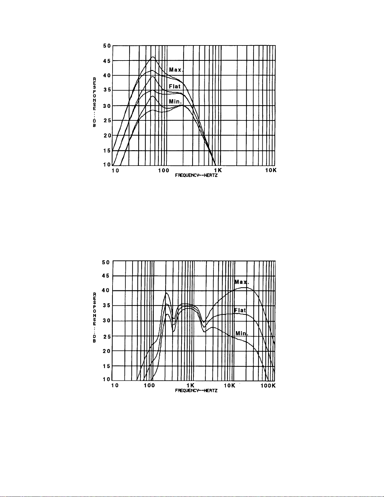
Frequency Response Curves
Bass channel frequency response curve with tone controls at min.,
max., and flat positions (for 30 and 200 mVrms input level)
Figure 1. Bass Channel Frequency Response Curve
Left/right channel frequency response with tone controls at min.,
max.,and flat positions.
Figure 2. Left/Right Channel Frequency Response Curve
5
Page 7
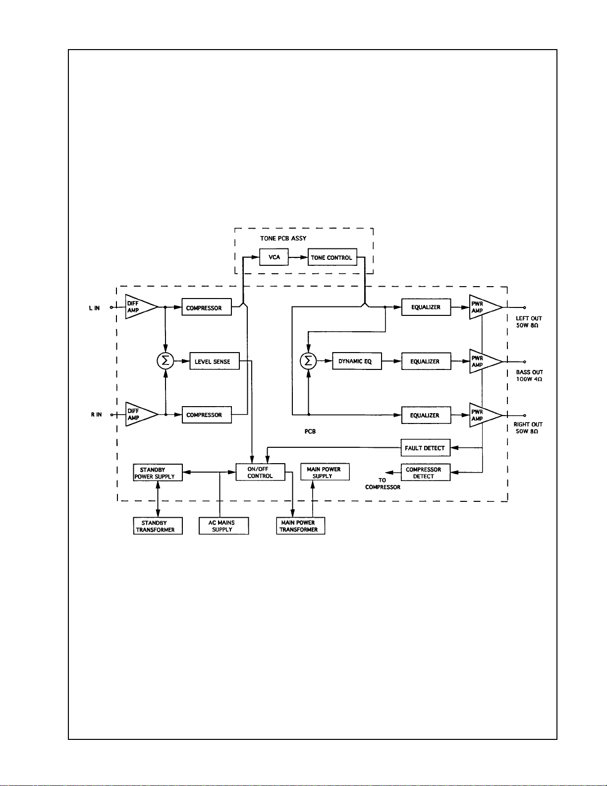
BLOCK DIAGRAM
MAIN
Figure 3. Main PCB (Amplifier) Block Diagram
6
Page 8

THEORY OF OPERATION
The following discussion references the Main PCB Schematic and Block Diagram. The
schematic is located in the back of this manual and the block diagram is shown in Figure 3.
GENERAL
The FreeSpace™business music system electronics module powers the FreeSpace loudspeaker system,which is a derivative of the AM-5
system, FreeSpace is meant to be used in conjunction with the customer's audio source.
The FreeSpace system offers the following features:
- Automatic turn-on/ turn-off (audio sense or signal from the customer's audio source)
- Automatic (Bose
®
patented) dynamic equalization
- Bi-amplification for better power distribution to speakers
- High Efficiency Class G Power Amp stages (100W + 50W +50W)
- Active equalization for smoother frequency response
- Amplifier short-circuit protection
- Bass/treble room compensation controls
- Differential input stage (to reject hum)
- Dynamic compressor to prevent amplifier output overload distortion
- Electronic remote volume
®
powered loudspeaker system. As a powered
BLOCK DIAGRAM DESCRIPTION
Refer to the block diagram and schematic mentioned above. For discussion of L/R channels,
only the right channel is discussed. Left channel operation is identical.
1. Power Supply
Two power supplies are used in the FreeSpace system. One is a low power regulated ±15VDC
supply used to power the signal processing circuitry, the other is the high voltage main power
supply used to power the three Class G power amplifier stages. Two voltages are provided for
class G operation, ±20VDC and ±40VDC. The regulated ±15VDC supply always remains
energized as long as the unit is wired to an active mains voltage source. The main power
amplifier supply is turned on and off by the audio sensing circuit (discussed elsewhere).
7
Page 9

2. Differential Amplifier
Audio input is at barrier strip P5, which is located on the I/O PCB Assembly (see the schematic
located in the back of this manual). This connects directly to the left and right differential
amplifier buffers on the Main PCB. This stage neatly accomplishes several functions: provides
rejection of common-mode interference (like hum) that might be picked up by the long audio
cable between the FreeSpace™ system and the customer's audio source; provides input
overload protection through diodes (D101-104); strips off radio frequency interference through
capacitors C203 and 204; provides DC blockage by capacitors C201 and 202; and provides
a 10 dB gain through op-amp U201 .
3. Compressor
U201 (pins 5,6,and 7), under normal audio conditions, operates as a conventional inverting opamp stage with a gain of 6 dB. However, when overload is present at the speaker outputs,
transistor U205 (pins 5,6 and 7) receives a turn-on signal from the compressor detect stage.
When this happens the transistor acts as a variable resistor to ground, and with resistor R207
forms a voltage divider network that attenuates the audio signal. The amount of attenuation
and timing action is carefully controlled by the compressor detect stage (discussed later).
4. Audio Sense
The FreeSpace system remains in standby mode until audio is detected at its inputs. Audio
sense occurs after the compressor gain stage where the left and right signals are summed
through resistors R222 and R224. The signal is preamplified by inverting op-amp summer
stage U203 (pins 1,2,and 3), and is presented at the pin 1 input of turn-on chip U204 (NJM2072).
Diodes D109 and D110 are necessary to prevent overload of the turn-on chip at high volume
levels. With audio input ≥0.3 mVrms, U204 pin 7 goes high, and through diode D111 turns on
transistor Q401. This triggers relay K1 to energize the main power transformer. Turn-on
(settling) time of the power amplifier section is approximately 80 ms.
Without audio input,U204 pin 7 will go low after approximately 90 seconds, and will de-energize
relay K1 and the main supply. This turn-off time is set by capacitor C217 .
5. Tone /Electronic Volume Control
A separate tone control PCB attaches to the Main PCB through a seven conductor ribbon cable
connector. Power is derived from the main board. The tone control is a standard Baxandall
circuit with +/- 6 dB bass and treble controls. Volume control function is accomplished through
the use of current-controlled amplifier IC U502 (CA3280). The gain of U502 is directly
proportional to the current flowing into pins 3 and 6 from transistor Q502. This current is
proportional to the voltage at the base of Q502. This voltage is adjusted by the external 10K
potentiometer that indirectly attaches across connector J502 through the I/O PCB barrier strip
terminal P5,pins 7 and 8. At minimum volume (0Ω between J502,pins 1 and 2),the voltage at
the base of Q502 should be .36 ± .1 VDC.
At maximum volume (10 KΩ between J502,pins 1
and 2),the voltage at the base of Q502 should be 4.6 ± .1VDC. A schematic is located at the
back of this manual.
8
Page 10

6. High Frequency Equalization
High frequency equalization is achieved through four cascaded active EQ stages consisting of
U101, U102, U103 and U104. The purpose of equalization is two-fold. (1) It provides very sharp
low frequency roll-off below 180 Hz (the crossover frequency of the acoustics) to prevent
overload of the L/R speakers; and (2) It provides finely tailored correction in the L/R speaker
pass band so that overall frequency response of the system is correct.
7. Automatic Dynamic Loudness
In order to compensate for the ear’s loss of bass response at low listening levels, a Bose
patented automatic loudness circuit is employed. This circuit automatically senses the volume
level of the incoming audio signal, and properly adjusts the amount of low frequency bass boost.
When the volume level is high, the frequency response of the circuit is flat. When the volume
level is decreased (at the customer's audio source or through the electronic volume control),
the low frequency gain is increased in the region between 50 and 150 Hz.
Circuit operation is as follows: After passing through the Tone Control PCB, audio at U201 and
U202 (pin 7) is summed by resistors R101 and R131. The AC signal at pin 5 of level detect opamp U203 is negative -peak detected, and is presented across emitter resistor R236. The peak
detected signal has a 4 second hold time, and a 4 sec / 10 dB release time constant which is
developed within the feedback loop of U203 (pins 5,6 and 7). The voltage across R236 is
converted to a current source through transistor Q203, and flows into pin 5 of transconductance
amp U206. U206 and U207 (pins 1,2 and 3) form a variable gain stage (delta-G). Action is
such that increased current into pin 5 of U206 causes gain of the stage to decrease.
The variable gain stage is followed by a 55 Hz, Q=2.3 band pass filter (U207 pins 5,6 and 7).
The output of this stage is summed through resistor R247 with the flat response signal present
at resistor R248. This creates a composite frequency response curve with varying levels of 55
Hz boost. The overall desired loudness contour response is visible at U208 pin 1.
®
8. Low Frequency Equalization
A single stage Sallen-Key 2nd order high-pass / low pass network (U208 pins 5,6 and 7)
provides bass channel equalization and low frequency roll-off to prevent subsonic low
frequency overload.
9. Power Amplifier
All three power amplifiers are of identical topology and use high efficiency Class G power amp
stages. The L/R amplifier channels are both rated at 50W. The bass channel is 100W, and
because of its higher power, uses higher current output transistors and slightly different
component values. Otherwise,operation is the same.
9
Page 11

The basic concept behind Class G operation is simple. It takes advantage of the fact that music,
even at loud volume settings, has only brief moments where peak voltage from the amplifier
is needed. Unfortunately, with conventional Class B amplifiers, this peak voltage is always
supplied to the output transistors and most of the time is wasted as heat. The result is that larger
and more expensive power supplies and heatsinks are needed (or power output transistors are
operated hotter with less reliability).
With Class G however, the amplifier operates off of two different power supply voltages. When
the music is low the amp runs off of the low voltage supply, thus conserving power. When
musical peaks occur, the amplifier “intelligently” switches to the higher voltage supply. On
average, this voltage “conservation” translates to efficiency almost double that of class B.
Detail operation of the amp is as follows: First, it is important to understand that a Class G amp
is really just a class B amp with special circuitry added to it to allow switching between two
different power supply voltages. In the case of the bass amplifier, this switching action is
accomplished on positive peaks by transistors Q335, Q334 and Q333, and on negative peaks
by transistors Q342,343, and Q344.
A positive signal at op-amp input U303 pin 3 causes op-amp supply current to flow into pin 7
through transistor Q336. Q336 is used simply to buffer the +40V high voltage amp supply down
to a safe +15V for the op-amp. This current also flows through resistor R353 and diode D325.
R353 and D325, together with driver transistor Q332 and R355, form a current mirror which
multiplies the current through Q336 by the ratio R353/R355. This increased current flows
through driver transistor Q332, through diode D330, and into the base of output transistor Q337.
The hFE current gain of Q337 (about 40) provides final current amplification before reaching
speaker output.
Class G switching action occurs as follows: the voltage at the anode of D330 tracks one diode
drop above the output voltage of the amp. When this voltage exceeds the nominal +20V power
supply rail transistor Q335 conducts. This in turn causes transistors Q334 and Q333 to turn
on. When Q333 turns on, it acts as a switch and connects the +40V supply present at its emitter
to the collector of output transistor Q337. When this occurs, the +20V supply, normally fed
through diode D329, is turned off because the +40V causes the diode to be reversed biased.
When the music voltage drops below +20V, the reverse happens. The +40V supply is turned
off, and the +20V supply is turned on again.
The power amplifier topology is complementary. Therefore, operation of the amplifier on
negative half cycles is identical to positive cycle operation except for component reference
designations.
10. Short Circuit Protection
The left and right power amp stages have short circuit protection. This is necessary to prevent
damage to the amplifier from possible customer misuse. For example, the customer could
accidentally short the speaker cable wires that connect to the cube speakers. If this happens,
all three amplifiers will momentarily mute for about 3-4 seconds, and will continue to mute until
the abnormal condition is removed.
10
Page 12

This is achieved with the use of a .12 Ω resistor (R313 for right channel) in series with each
amplifier output. Under normal conditions, peak current to the 8 Ω speakers should never
exceed 3.5 amperes. If current flow exceeds 4.5 amperes, then Q309 will conduct and trigger
monostable multivibrator circuit U401 (pins 1,2 and 3). Pin 1 will go high (for about three
seconds) and will trigger mute transistors Q409 and Q408 through diode D406. Turn-on of
Q408 causes all three amplifiers to mute. Referring to the bass power amplifier, actual muting
occurs by turning on transistors Q331 and Q340, which cause both driver transistors (Q332 and
Q341) to turn off. When the driver transistors are off ,there can be no current flow through the
output transistors.
11. DC Offset Protection
If any one of the three amplifier channels should fail, it is likely that a large DC voltage will occur
at the output of that channel. If this occurs, the DC offset detect circuit will cause the
FreeSpace™ main power supply to shut down. It will remain shut-down until the unit is
disconnected from the power source. This provides a safe indication to the customer that the
unit requires service.
Detailed operation is as follows: Outputs of each amplifier are summed by resistors R407,R408
and R409, and low pass filtered by capacitor C401. For a sustained DC offset ,capacitor C401
will charge either negative or positive. A positive offset will trigger transistor Q404. A negative
offset will trigger transistor Q405. This in turn causes transistor Q403 to conduct, and latches
Q404 permanently on. Transistor Q402 then shorts the base of Q401 to ground. Q401 is the
transistor that controls turn-on of relay K1 that is used to energize power transformer T2.
Therefore, when Q401 is disabled, main power is shut down.
12. Compressor Detect
The output of each amplifier is half-wave detected through diodes D409,D410 and D411
respectively. This voltage is divided down by resistors R422 and R423, and is presented at the
emitter of transistor Q410. Power supply voltage is similarly divided down by R425 and R426,
and is presented at the base of Q410. Diodes D419 and D420 simulate the saturation voltage
drop that occurs in the power amp stage. Therefore, when audio output of any amplifier comes
within two volts of the instantaneous power supply voltage, Q410 will conduct, which signals
the compressor (limiter) to act. Current from Q410 charges hold capacitor C405 and release
capacitor C422. Voltage at C405 is buffered by transistor U205 (pins 1,2 and 3) and decreased
down to a logarithmic voltage by resistor R438 and transistor U205 (pins 12,13 and 14). This
voltage is then presented to the base of compressor transistors U205 (pins 5,6 and 7) and U205
(pins 8,9 and 10) which are described in the compressor section.
The DC control voltage present across capacitor C405 is derived through the use of an
improved hold and release characteristic. This results in lower compressor distortion. In
conventional limiters this DC control voltage is derived by a simple series diode and parallel RC
network to ground. Unfortunately, for low frequency overload, this results in substantial ripple
voltage present on the DC gain control voltage. This results in the all too common problem of
mid-range voices or instruments being badly “modulated” by low frequency overload. This
problem is solved by having two separate capacitors, one that “holds” the smooth DC voltage
just long enough to prevent low frequency ripple (approximately 40ms) and the other (C422)
that quickly releases the hold cap (through diode D412) at the proper time to maintain overall
100ms release time.
11
Page 13

NOTES FOR FUTURE REFERENCE
12
Page 14

DISASSEMBLY/ ASSEMBL Y PROCEDURES
NOTE: Figure numbers of exploded views will
be referred to throughout these procedures.
Certain parts will be referenced. The item
number in each figure which corresponds to the
part will be enclosed in parentheses-i.e.-rod
cover (4).
1. Mounting Hardware Removal
NOTES: Refer to Figure 4 for Procedures 1 and 2
unless otherwise specified.
Older versions of the unit contain different
mounting hardware than newer versions of the
unit.
If you have an older version of the unit,the
mounting hardware will consist of 2 threaded tie
rods (not shown) and 4 acorn nuts with washers
(not shown). Refer to step A. for disassembly
instructions.
If you have a newer version of the unit,the
mounting hardware will consist of 2 long screws
(3) which thread into 2 pem nuts (part of the
mounting straps (5). These screws have a hex
head with a built-in washer. Some newer units also
have 1 additional washer located on the end of
each screw. Refer to step B. for disassembly
instructions.
A. For older units: Remove 1 7/16" acorn nut
(with washer) from each threaded tie rod. Another
tool may be needed to hold the acorn nut on the
other end of each rod to prevent the rod from
turning.
Slide each tie rod through the holes located in the
mounting straps. (The rod covers (4) will also slide
off). Remove the mounting straps by pulling them
carefully away from the unit.
2. Mounting Hardware Replacement
A. For older units: Position the 2 mounting straps
(5) so that their screw holes line up with the 2
wide "channels" (between the fins) on each edge
of the heatsink (Figure 6,Item 1). See Figure 4
for proper strap orientation. Slide the 2 threaded
tie rods through the holes located in the mounting
straps. Make sure that the rod covers (4) are in
place before securing the rods to the straps.
NOTE: 2 of the acorn nuts (not shown) should
already be secured on the end of each tie rod.
B. Replace 2 of the 7/16" acorn nuts (with
washers). Another tool may be required to hold
the other acorn nut on each rod.
C. For newer units: Position the 2 mounting
straps so that their screw holes line up with the 2
wide "channels" (between the fins) on the edges
of the heatsink. See Figure 4 for proper strap
orientation. Some newer units have washers that
are located on each screw. Make sure that the
washers are in place before sliding the rod covers
on. Make sure that the rod covers are in place
before securing the screws to the straps. Thread
the 2 long screws (3) into each pem nut (part of
the mounting straps). Make sure that both long
screws are securely fastened.
3. Junction Box Cover Removal
B. For newer units: Unscrew the 2 long screws
from the 2 pem nuts (part of the mounting
straps). Pull the screws through the holes
located in the mounting straps. (The rod covers
will also slide off). On newer units there may also
be 1 washer located on the end of each screw. It
is not necessary to remove either washer.
Remove the straps by pulling them carefully
away from the unit.
NOTE: Refer to Figure 4 for Procedures 3 and 4
unless otherwise specified.
A. Loosen the 4 screws (9) which secure the
junction box cover (8). Slide the cover so that the
screws are released from the smaller section of
the screw hole. Lift the cover away from the
junction box (7).
13
Page 15

4. Junction Box Cover Replacement
7. Tone Control PCB Assembly Removal
A. Position the junction box cover (8) over the 4
screws (9) still secured to the junction box (7).
Lower the cover into place.
B. Slide the cover until all 4 screws are engaged
with the narrow slot in each screw hole. Secure
the cover to the junction box with the 4 screws.
5. Panel Assembly Removal
A. Remove the mounting hardware (Procedure
1) and the junction box cover (Procedure 3).
NOTE: Refer to Figure 4 for Procedures 5 and
6 unless otherwise specified.
B. Remove 14 screws (2) which secure the panel
assembly (1) to the unit.
NOTE: If the panel assembly does not need to
be completely removed,then it may not be
necessary to unhook the connectors as directed
in step C.
NOTE: Refer to Figure 4 for Procedures 7 and
8 unless otherwise specified.
A. Remove the mounting hardware (Procedure
1), junction box cover (Procedure 3),and panel
assembly (Procedure 5).
B. Remove the 2 control knobs (21) using either
your fingers or a flat blade screwdriver.
C. Remove the 2 3/8" hex nuts (22) and washers
(23) which secure the PCB (24) to the unit.
D. Push the control knob shafts through the holes
in the unit and carefully lift the PCB away from
the unit.
8. Tone Control PCB Assembly Replacement
A. Slide the control knob shafts through the holes
in the unit. Make sure that the PCB is solder side
up.
C. Unhook connectors J303 (woofer output) and
J101 from the Main PCB Assembly (Figure 6,
Item 13) and connector J502 from the Tone
Control PCB Assembly (24).
D. Carefully lift the panel assembly away from
the unit.
6. Panel Assembly Replacement
A. Lower the panel assembly (1) into position.
B. Plug in connectors J303 (woofer output) and
J101 to the Main PCB Assembly (Figure 6,Item
13) and connector J502 to the Tone Control PCB
Assembly (24) if they were previously
disconnected.
C. Secure the panel assembly to the unit with 14
screws (2).
D. If no further troubleshooting is required,reinstall the junction box cover (Procedure 4) and
the mounting hardware (Procedure 2).
B. Secure the PCB (24) to the unit with 2 3/8"
hex nuts (22) and washers (23).
C. Replace the 2 control knobs (21) by pushing in
gently towards the unit. The knobs are keyed and
will only fit one way.
D. If no further troubleshooting is required,reinstall the panel assembly (Procedure 6) ,the
junction box cover (Procedure 4) ,and the
mounting hardware (Procedure 2).
9. Woofer Removal
NOTE: Refer to Figure 4 for Procedures 9 and
10 unless otherwise specified.
A. Remove the mounting hardware (Procedure
1),junction box cover (Procedure 3),and the
panel assembly (Procedure 5).
B. Remove the 6 screws (2) which secure the
woofer (19) to the unit, and lift the woofer
carefully away from the unit.
14
Page 16

10. Woofer Replacement
A. Cut the wires connected to the woofer
terminals as close to the terminals as possible.
(These wires are the woofer connection cable
(20)).
B. Strip the ends of the cable and connect to the
replacement woofer (19). Make sure that the red
wire is connected to the positive (+) terminal and
the black wire is connected to the negative (-)
terminal.
NOTE: If no further troubleshooting is
required,restore any connections that may have
been desoldered or disconnected.
C. Replace the panel assembly (Procedure
6),junction box cover (Procedure 4),and
mounting hardware (Procedure 2).
13. I/O PCB Assembly Removal
NOTE: Refer to Figures 6 and 9 for Procedures
13 and 14 unless otherwise specified.
C. Secure the woofer to the unit using 6 screws
(2).
D. Re-connect the woofer connection cable (20)
to the Main PCB Assembly (Figure 6,Item 13)connector J303. Make sure all other connections
to the appropriate PCBs are restored. Repeat the
woofer test procedures.
E. If no further troubleshooting is required, reinstall the panel assembly (Procedure 6),junction
box cover (Procedure 4),and the mounting
hardware (Procedure 2).
11. Main PCB (Amplifier) Assembly Removal
NOTE: Refer to Figure 6 for Procedures 11 and
12 unless otherwise specified.
A. Remove the mounting hardware (Procedure
1),junction box cover (Procedure 3),and the
panel assembly (Procedure 5).
A. Remove the mounting hardware (Procedure
1),junction box cover (Procedure 3), and panel
assembly (Procedure 5).
B. Remove the 2 11/32" nuts (Figure 6,Item 12)
that secure the PCB (Figure 6,Item 11) to the
rear panel (Figure 6,Item 3). Lift the PCB
carefully away from the panel.
NOTE: Unhook connectors P1 through P4 only if
necessary.
C. The barrier strip connector (Figure 9,Item 3)
is soldered to the PCB. Desolder the 16
connections.
NOTE: If the barrier strip connector needs to be
replaced, remove the 4 screws (Figure 9,Item 4)
which secure it to the I/O plate (Figure 9,Item 1).
D. Lift the PCB carefully away from the I/O plate.
B. Remove 9 screws (14) which secure the PCB
(13) to the rear panel (3).
C. Remove 4 screws (4) which secure the
heatsink couplers to the rear panel.
12. Main PCB (Amplifier) Assembly Replacement
A. Secure the 2 heatsink couplers to the rear
panel (3) with 4 screws (4).
B. Secure the PCB to the rear panel (3) with 9
screws (14).
14. I/O PCB Assembly Replacement
A. Align the PCB (Figure 6,Item 11) and I/O
plate (Figure 9,Item 1). The shaft of
potentiometer R8 fits through a hole in the plate.
NOTE: If the barrier strip connector (Figure
9,Item 3) was replaced,proceed as follows: Align
the I/O plate gasket (Figure 9,Item 2) with the
I/O plate,and then secure the connector to the
plate with 4 screws (Figure 9,Item 4).
B. The barrier strip connector needs to be
soldered to the PCB. Solder all 16 connections
to the PCB.
15
Page 17

C. Lower the PCB through its slot on the rear
panel (Figure 6,Item 3).
D. Secure the PCB to the panel with 2 11/32" hex
nuts (Figure 6,Item 12).
D. If no further troubleshooting is required,re-
install the panel assembly (Procedure 6),junction
box cover (Procedure 4),and mounting hardware
(Procedure 2).
NOTE: If connectors P1 through P4 were
unhooked,re-connect them.
E. If no further troubleshooting is required,reinstall the panel assembly (Procedure 6),junction
box cover (Procedure 4),and mounting hardware
(Procedure 2).
15. Power Transformer (T2) Removal
NOTE: Refer to Figure 4 for Procedures 15
and 16 unless otherwise specified.
A. Remove the mounting hardware (Procedure
1),junction box cover (Procedure 3),and panel
assembly (Procedure 5).
B. Remove 4 5/16" hex nuts (15) and washers
(16) that secure the power transformer (14) to the
rear panel (Figure 6,Item 3).
17. "Keep Alive" Transformer (T1) Removal
NOTE: Refer to Figure 6 for Procedures 17 and
18 unless otherwise specified.
A. Remove the mounting hardware (Procedure
1),junction box cover (Procedure 3),and panel
assembly (Procedure 5).
B. Remove 2 1/4" nuts (9) which secure the
transformer (8) to the rear panel (3).
C. The transformer primary and secondary wires
are hardwired to the Main PCB Assembly
(13).Make a note of the wire locations and
desolder all connections.
D. Lift the transformer away from the panel.
18. "Keep Alive" Transformer (T1) Replacement
C. Unhook the transformer primary connector
J402 and the transformer secondary connector
J403 from the Main PCB Assembly (Figure
6,Item13).
D. Lift the transformer carefully up from the
panel.
16. Power Transformer (T2) Replacement
A.Position the transformer (14) in its original
location.
B. Secure the transformer to the rear panel
(Figure 6,Item 3) with 4 5/16" hex nuts (15) and
4 washers (16).
C. Re-connect the transformer primary connector
J402 and the transformer secondary connector
J403 to the Main PCB Assembly (Figure 6,Item
13).
A. Secure the transformer (8) to the rear panel
(3) with 2 1/4" nuts (9).
B. Re-connect the primary side and secondary
side connections to the Main PCB Assembly (13)
as follows:
• Solder the red primary wire to T404.
• Solder the black primary wire to T403.
• Solder the blue secondary wire to T405.
• Solder the white secondary wires (2) to T402
and T401 (order is irrelevant).
C. If no further troubleshooting is required,reinstall the panel assembly (Procedure 6),junction
box cover (Procedure 4), and mounting
hardware (Procedure 2).
16
Page 18

Satellite Procedures
NOTE: Refer to Figure 7 for an exploded view of
the satellite. Certain parts will be referred to in
these procedures. The item number which
corresponds to the part will be enclosed in
parentheses-i.e.-grille (3).
B. Connect the red wire to the positive (+)
twiddler terminal and the black wire to the
negative (-) twiddler terminal.
C. Lower the twiddler into the satellite enclosure
and secure the twiddler to the enclosure with 4
screws (7). Repeat the satellite test procedures.
1. Grille Removal
A. Grasp the top and bottom of the grille and
grille frame (3,5). Pull the assembly carefully
away from the satellite.
2. Grille Replacement
A. Align the grille feet (not shown) with the 4
holes in the satellite enclosure. Push the
assembly gently into place.
3. Twiddler Removal
A. Remove the 4 screws (7) holding the twiddler
(6) in place. Lift the twiddler out and cut the wires
connected to the twiddler as close to its terminals
as possible.
4. Twiddler Replacement
A. Strip the wires and connect to the replacement
twiddler (6).
5. Terminal Cover Removal
NOTE: There are catches on the top and bottom
(inside) of the terminal cover (10) that hook it into
the satellite enclosure. Take care when removing
the cover.
A. Using your fingers or a flat blade
screwdriver,pull the terminal cover carefully from
the satellite enclosure using the recesses in the
cover.
6. Terminal Cover Replacement
A. Snap the terminal cover (10) carefully into
place on the satellite enclosure.
7. Guillotine Connector Removal
A. Remove 2 screws (7) which hold the
connector (9) in place.
8. Guillotine Connector Replacement
NOTE: The positive (+) terminal of each twiddler
is marked with a red dot.
A. Secure the connector (9) to the satellite
enclosure with 2 screws (7).
17
Page 19

TROUBLESHOOTING TIP FOR HUM AND RFI REMOVAL
Hum and RFI (Radio Frequency Interference) are the most common problems when using
unbalanced signal sources and long signal leads. Once you have connected all equipment properly
and made all chassis grounds,adjust the BALANCE TRIM potentiometer located in the junction box.
See the figure below for reference. This shaft can be adjusted with a screwdriver. It is located to the
right of the ( ) symbol,just above the shield label in the SIGNAL INPUT section of the junction
box. Be careful not to contact the AC mains terminals,since this task must be performed with the
power on.
First,turn your signal source electronics off,but do not disconnect the signal leads. If the interference
stops,it is not the signal leads,but the equipment. Second,turn the remote volume control to full
volume (or disconnect the volume control leads). Then,adjust the potentiometer while listening for
minimum interference. Since the system has an automatic turn-on circuit,the system will stop
amplification less than 2 minutes after you turn off the source electronics. If adjustment is not
completed in this time,re-trigger the circuit. You can momentarily turn on the source electronics
(with a signal) or sometimes touch one of the audio terminals with a bare finger. Do not assume that
turning the power switch on and off will trigger the circuit. The internal protection circuitry may
interpret this action as a supply fault and keep the system off for at least two minutes.
At some point in a full rotation of the potentiometer,interference will drop then increase again,so you
must adjust to this minimum point. If this adjustment fails to remove interference,more tests should
be performed before blaming the amplifier or the cabling. Disconnect the signal leads from the
source equipment. Temporarily connect a 1 KΩ resistor between the two signal terminals of the
signal cable(s). Adjust the trim pot again. If the interference is eliminated,the fault is with the source
electronics. If cable termination has been done according to recommendations,then the problem
may still be with the type of isolation provided by equipment with unbalanced outputs. The "ironclad" solution to isolation problems is to use an audio isolation transformer for each channel. This
converts the unbalanced output into a balanced output with shield connection. If interference is still
audible,then a very large signal is being picked up. This may require re-routing of the audio leads,or
even tracking down defective electrical equipment such as fluorescent light ballasts or large
horsepower motors. Large and very close broadcast antennas as well as high power CB radios can
also be a problem. Fortunately,interference of such severity is rarely a problem if a quality
installation of the Free Space system is done.
18
Page 20

TEST PROCEDURES
Satellite Test Procedures
NOTE: Use these procedures only when
satellites come in to be serviced (without the
bass module).
1. Sweep Test
A. Connect an oscillator to a power amplifier.
Adjust the amplifier output to 4 Vrms. Connect
the amplifier leads to the satellite (cube speaker)
input terminals. Sweep the oscillator from 200 Hz
to 5 kHz. If any twiddler buzzes or sounds
distorted,replace it.
2. Phase Test
NOTE: Supply voltage should only be
momentarily applied to the satellite input
terminals to avoid possible damage to the
twiddlers.
1. Sweep Test
NOTE: This test can be performed with a fully
assembled bass module.
A. Connect an oscillator to the module’s L/R
audio input terminals. Adjust the oscillator to 100
Hz,185 mVrms. Sweep the oscillator from 10300 Hz. There should not be any
loud,extraneous sounds. If there are any loud
buzzes or distortion, the woofer may be
defective. The Main PCB (amplifier) should also
be checked for possible problems.
NOTE: There should not be any buzzes or rattles
from within the module. Redress any wire or
component that buzzes or rattles.
2. Tone Control Test
NOTE: This test can be performed with a fully
assembled module.
A. Set a DC power supply to 2 volts. To ensure
that each twiddler is connected in phase, connect
the positive supply lead to the positive (+)
satellite input terminal (red) and the negative
supply lead to the negative (-) satellite input
terminal (black). The twiddler should move
outwards with the application of the supply
voltage.
NOTE: If any twiddler cone deflects inwards or
does not move,check all connections.
Bass Module Test Procedures
NOTES: Use these procedures only when a
module comes in to be serviced (without
satellites). All tests should be performed with the
bass and treble control knobs in the normal or
"detent" position. Remove the junction box cover
using Procedure 3 in the Disassembly/
Assembly Procedures section in order to
access the connection terminals for this unit.
A. Connect an oscillator to the module’s L/R
audio input terminals. Adjust the oscillator to 100
Hz,185 mVrms.
B. Rotate the bass control knob fully clockwise
and counterclockwise from its center or “normal”
position. The bass level should increase and
decrease cleanly without making a scratchy
noise. Clean or replace any potentiometer that
makes this noise.
C. Repeat this procedure for the treble control
using a frequency of 4 kHz.
NOTE: Refer to Figures 1 and 2 for an
approximate bass and treble response for this
procedure.
19
Page 21

3. Frequency Response of L/R (Twiddler) Channels
4. Twiddler Power Output Test
NOTE: This test can be performed with a fully
assembled module.
A. Connect an oscillator to the module’s L/R
audio input terminals. Adjust the oscillator to 1
kHz,30 mVrms for a 0 dB reference.
NOTE: There are 2 sets of twiddler output
terminals for each channel. Refer to the I/O PCB
Schematic before attempting any connections.
For the left channel,connections should be made
to pins 8 (+) and 5 (-). For the right
channel,connections should be made to pins 4
(+) and 1 (-). This note applies to Procedures 3
through 6.
B.Connect an 8Ω resistive load across either the
left or right twiddler output terminals. Using a dB
meter,measure the response according to the
chart given below.
C. Repeat this test for the other channel.
NOTE: This test can be performed with a fully
assembled module. Refer to the second note in
Procedure 3 before making any connections.
A. Connect an 8Ω resistive load and a voltmeter
across either the left or right twiddler output
terminals.
NOTE: These measurements can be obtained at
120 and 240 V. Results will vary depending on
the line voltage used.
B. Connect an oscillator to the module’s L/R
audio input terminals. Adjust the oscillator to 1
kHz, 465 mVrms.
C. Measure the voltage across the load. It should
be approximately 20 volts (50 watts).The signal
should look undistorted when viewed on an
oscilloscope.
5. Twiddler Short Circuit Protection Test
Frequency Relative Response
100 Hz -17.6 dB ± 2.0 dB
210 Hz +1.3 dB ± 1.5 dB
320 Hz - 6.2 dB ± 1.8 dB
1 kHz 0 dB
1.8 kHz -6.5 dB ± 1.5 dB
10 kHz -2.0 dB ± 1.5 dB
36 kHz -5.3 dB ± 2.0 dB
NOTES: This test can be performed with a fully
assembled module. Refer to the second note in
Procedure 3 before making any connections.
A. Adjust the oscillator to 400 Hz, 180 mVrms.
Connect an 8Ω resistive load and a voltmeter
across either the left or right twiddler output
terminals. The output voltage should measure
approximately 8 Vrms. Momentarily short the left
or right twiddler output terminals. The signal
should mute for approximately 2-3 seconds.
6. Compressor Test
NOTE: This test can be performed with a fully
assembled module. Refer to the second note in
Procedure 3 before making any connections.
A. Connect an oscillator to the module's L/R
audio input terminals. Adjust the oscillator to 1
kHz,1.1 Vrms.
20
B. Connect an 8Ω resistive load across either the
left or right twiddler output terminals.
Page 22

C. Connect a distortion meter across either the
left or right twiddler output terminals. The
distortion should be less than 3.0% THD.
D. Repeat the test for the other channel.
7. Air Leak Test
NOTE: This test can be performed with a fully
assembled module.
A. Connect an oscillator to the module’s L/R
audio input terminals. Adjust the oscillator to 40
Hz,185 mVrms. Listen for air leaks around the
cabinet,edge of the amplifier panel,edge of the
heatsink,around the barrier strips (inside junction
box),tone control knobs,power switch, and panel
screws. If there is a“whooshing”noise,there is
probably an air leak in one of these
locations.Repair any air leaks as required.
8. Woofer Rub and Tick Test
A. Make up a temporary set of connections to the
woofer output connector J303 (disconnect from
the woofer). The positive wire should be
connected to pin 2 and the negative wire should
be connected to pin 1 . See the figure below for
a reference.
Pin 1 Pin 2
B. Connect an oscillator to the module’s L/R
audio input terminals. Adjust the oscillator to 100
Hz,30 mVrms for a 0 dB reference.
C. Connect a 4Ω resistive load across the
woofer output. Using a dB meter,measure the
response according to the chart below.
NOTE: In order to perform this test,it is necessary to access the woofer. Refer to Procedure
9,steps A. and B.,Woofer Removal,in the
Disassembly/Assembly Procedures section.
A. Connect an oscillator to the module’s L/R
audio input terminals. Adjust the oscillator to 10
Hz,185 mVrms. No extraneous noises such as
rubbing,scraping or ticking should be heard.
NOTE: To distinguish between normal
suspension noise and rubs or ticks,displace the
cone on the woofer slightly with your fingers. If
the noise can be made to go away or get worse,it
is a rub or a tick and the woofer should be
replaced. If the noise stays the same,it is normal
suspension noise and the woofer is fine.
Suspension noises will not be heard with
program material.
9. Frequency Response of Bass Channel
NOTE: In order to perform the next three tests,it
is necessary to access the panel assembly which
contains the Main PCB. Refer to Procedure
5,Panel Assembly Removal, in the
Disassembly/Assembly Procedures section.
Frequency Relative Response
20 Hz -10.0 dB ± 1.5 dB
55 Hz +4.8 dB ± 1.8 dB
100 Hz 0 dB
200 Hz -1.0 dB ± 1.5 dB
400 Hz -11.4 dB ± 1.5 dB
10. Bass Channel Dynamic EQ Gain
NOTE: Use the same test setup as test
Procedure 9.
A. Adjust the oscillator to 55 Hz,200 mVrms.
The gain relative to the input should be
approximately 35.1 dB.
21
Page 23

11. Woofer Power Output Test
2. System Sweep Test
NOTE: Use the same test setup as Procedure
9,except remove the dB meter.
A. Connect a voltmeter across the 4Ω resistive
load.
NOTE: These measurements can be obtained at
120 and 240 V. Results will vary depending on the
line voltage used.
B. Adjust the oscillator to 100 Hz,555 mVrms.
C. Measure the voltage across the load. It should
be approximately 20.0 volts (100 watts). The
signal should look undistorted when viewed on an
oscilloscope.
Complete System Tests
NOTE: Use these procedures when a complete
FreeSpace™ business music system (module and
satellites) comes in to be serviced. All procedures
listed under Bass Module Test Procedures can
be used to test a complete system except as
indicated below.
1. System Phase Test
A. Use the procedures already given for the
satellites and the module,except use 185 mVrms
for both parts of the test. Use Procedure #1 under
Satellite Test Procedures and Procedure #1
under Bass Module Test Procedures. Make sure
that the satellites are connected to the bass
module.
3. Volume Control Test
A. Connect an oscillator to the module's L/R audio
input terminals. Adjust the oscillator to 4 kHz,185
mVrms.
B. Connect a set of satellites to either the 2 left or
the 2 right channels.
C. Attach the remote volume control to the
positive (+) and negative (-) volume control
terminals. At the 0 volume setting,the audio signal
should be faint or nonexistent,and at the
maximum volume setting,the audio signal should
be loud.
D. If there is no remote volume
control,momentarily short across the positive (+)
and negative (-) volume control terminals. The
signal should be faint or nonexistent.
A. Use the procedures already listed for the
satellites and the module. Use Procedure #2
under Satellite Test Procedures and Procedure
#10 under Bass Module Test Procedures.
22
Page 24

PARTS LISTS AND EXPLODED VIEWS
The following section contains parts lists and exploded views for the FreeSpace™ business
music system. The parts lists are broken down as follows:
-Bass Module Parts List and Exploded View.
-Bass Module Packaging Parts List and Exploded View
-Satellite Parts List and Exploded View.
-Satellite Packaging Parts List and Exploded View.
-Electrical and Mechanical Parts Lists. PCB layouts and schematics are located in
the back of the service manual.
NOTE: The notes section for the entire parts list is contained on page 24.
23
Page 25

PARTS LIST NOTES
1. This part is not normally available from Customer Service. Approval from the Field Service
Manager is required before ordering.
2. Refer to the Panel Assembly Parts List for parts located on the panel.
3. Refer to the Electrical Parts List for components located on this PCB. Components
with 500 series designators are located on this PCB.
4. This part is not illustrated.
5. This part replaces the original hardware which consisted of: 2 threaded tie rods, P/N 131032-4,
and 4 acorn nuts, P/N 145550.
!
6. This part is critical for safety purposes. Failure to use a substitute replacement with the same
safety characteristics as the recommended replacement part might create shock,fire and/or other
hazards.
7. Current production units slated for US and Japanese markets do not have this hardware
mounted on the junction box.
8. Current European units should contain two owner's manuals: the original manual, P/N 145549,
and the German version of the manual, P/N 149629.
9. Refer to the Electrical Parts List for components located on the PCB assemblies. 100-400 series
designators are located on the Main PCB and 0-99 designators are located on the I/O PCB.
10.Recent production runs of the bass module have 1 washer added to each long screw (Item 3 on
the Bass Module Parts List). This part is not illustrated in Figure 4,but a figure is provided here for
reference.
Long Screw
Washer
24
Page 26

Bass Module Parts List (Figure 4)
Item
Number
Description Part Number Qty.
Per
Module
1 Panel Assembly-120V 145530-1 1 1,2
Panel Assembly-230V 145530-2 1 1,2
Panel Assembly-100V 145530-3 1 1,2
2 Screw-HIRS,8-10x1,PAN,XREC/SQ 137527-16 20
3 Screw-Mach.,1/4 x 20,Hex Wshr. Hd. 148658 2 5
4 Cover-Rod 145983 2
5 Strap-Mounting,Black 145554-01 2
Strap-Mounting,White 145554-02 2
6 Cover-Terminal Block,Yellow 147524-32 1
7 Box-Junction,Black 145107-01 1
8 Cover-Junction Box 145108-01 1
9 Screw-Tapp,8-32 x 9/16,PAN,XRC 145727-09 4
See Note
10 Nut-Hex,Stnd.,Washer,KEPS 118260-08 4
11 Bushing-Rubber 146046 2 7
12 Plate-Anti-rotation 146047 1 7
13 Bushing-Strain relief 146048 1 7
14 Power Transformer-EI96,100/120V,T2or 145526 1 6
!
Power Transformer (alternate),T2
Power Transformer-220/240V,T2
135964 1 6
137819 1 6
15 Nut-Hex,M5 137448 4
16 Washer-M5 138513 4
17 Isolator-Vibration 140343 4
18 Cable Tie 135540 1
25
Page 27

Bass Module Parts List (Continued)
Item
Number
Description Part Number Qty.
Per
Module
19 Woofer-8" 146928 1
or
Woofer-8" (alternate) 142322 1
20 Cable-Woofer Connection 147795 1
21 Knob 136139 2
22 Nut-Hex 137446 2
23 Washer-1/4",Steel 131263-25 2 10
24 PCB Assembly-Tone Control 145525 1 1,3
-
Label-Tone Control 138446 1 4
See Note
26
Page 28

Figure 4. Bass Module Exploded View
27
Page 29

Bass Module Packaging Parts List (Figure 5)
Item
Number
Description Part Number Qty.
Per
Carton
1 Bracket-Wall Mount,Black 145553-01 1
2 Volume Control-Arctic White
(US)
Volume Control-Arctic White
135209-2
170245-01
1
1
(Eur.)
- Polybag (Volume Control) 143393 1
3 Insert-Diecut,Freespace 149240 1
4 Literature Kit-120V 146091-1 1
Literature Kit-230V 146091-2 1
Literature Kit-100V 146091-3 1
which consists of:
A Owner's Manual 145549 1 8
Owner's Manual (Eur.) 149629 1 8
B Warranty Card (US) 139610 1
Warranty Card (Eur.) 135970 1
C Polybag (Literature Kit) 103351 1
D Warranty Service List (US) 122766 1
See Note
E Envelope-Warranty Registration (US) 123001 1
Envelope (Eur.,Japan) 128450 1
F Wrench-Allen, 3/16" 145726 1
G Clip-U,1/4-20 145728 2
H Screw-Mach.,1-1/4",Socket Hd. Cap 145767-20 2
5 Packing-End Cap,EPS 139955 4
6 Polybag (Module) 137847 1
7 Carton 145531 1
28
Page 30

Figure 5. Bass Module Packaging Exploded View
29
Page 31

Panel Assembly Parts List (Figure 6)
Item
Number
Description Part Number Qty.
Per
Assembly
1 Heatsink 145536 1 1
2 Gasket-Heatsink 145537 1
3 Panel-Mounting,Rear 144495-01 1 1
4 Screw-
Thrd. Form,PAN,4-20 x 3/8"
139761-06 15
5 Connector-Barrier Strip,3P 145543-3 1
6 Gasket-Barrier Strip,3 Term. 145544 1
7 Screw-
Tapp,6-32 x 3/4, PAN, XREC
146093-12 2
8 Transformer-Keep Alive,
!
145527 1 6
EI41/120V,T1 (US,Japan)
Transformer-Keep Alive,
146977 1 6
EI41/220V,T1 (Eur.)
See Note
9 Nut-KEP, #4-40 118260-04 2
10 Switch-Rocker, SPST, 11A 145541 1 3
!
11 PCB Assembly-I/O 145546 1 1,9
12 Nut-Hex,STND.,Washer,KEPS 118260-08 2
13 PCB Assembly-Main 145524 1 1,9
14 Screw-
Mach.,#6-32 x 5/16,PAN,XREC
146092-05 9
15 Cable Assembly-Volume Control 145539 1
16 Cable Tie 135540 3
17 Fuse-Slo-Blo,2.5A,5 x 20mm,
!
UL,FS1 (US,Japan)
Fuse-Slo-Blo,1.6A,5 x 20mm,
143668-2500
140346-1600
1 6
1 6
VDE,FS1 (Eur.)
18 Nut-Hex, #8-32, Steel 103237-832 1
30
Page 32

Figure 6. Panel Assembly Exploded View
31
Page 33

Satellite Parts List (Figure 7)
Item
Number
Description Part Number Qty.
1 Logo-White on Black 123981-1A2 1
Logo-White on Grey 123981-1B3 1
2 Nut-Push On,.078 125786 2
3 Grille-Black 145401-1 1
Grille-White 145401-2 1
4 Grille Insert-Left,Black 142080-11 1
Grille Insert-Right,Black 142080-21 1
5 Grille Frame-Left,Black 145396-11 1
Grille Frame-Left,White 145396-13 1
Grille Frame-Right,Black 145396-21 1
Grille Frame-Right,White 145396-23 1
6 Twiddler,2-1/4" (Gasket-Backed) 147525 1
7 Screw-HIRS,6-10x1/2,PAN,XREC 124773-08 6
See Note
Per
Satellite
8 Batting-Polyester 116082 N/A 1
9 Connector,Terminal Strip 136547 1
10 Terminal Cover-Left,Black 136546-11 1
Terminal Cover-Left,White 136546-13 1
Terminal Cover-Right,Black 136546-21 1
Terminal Cover-Right,White 136546-23 1
32
Page 34

Figure 7. Satellite Exploded View
33
Page 35

Satellite Packaging Parts List (Figure 8)
Item
Number
Description Part Number Qty.
Per
Carton
1 Polybag (Satellite Parts) 144677 4
2 Tape-Bag,Sealing 148425 4 1
3 Bracket-Black 149303-1 4
Bracket-White 149303-2 4
4 Wrench-Allen,3/32 141109 1
5 Sheet-Instruction 145824 1
6 Packing-Divider 145395 1
7 Packing-Tape Tube 146468 1
8 Packing-Insert 145399 2
9 Carton-Satellites 145398 1
See Note
Figure 8. Satellite Packaging Exploded View
34
Page 36

Electrical and Mechanical Parts Lists
The next section of this manual contains the electrical and mechanical parts lists. The
electrical parts list contains all electrical components located on the Main PCB,Tone
Control PCB and I/O PCB Assemblies. Each board has a specific series of reference
designators which are coded as follows:
• 0-99 series reference designators correspond to the I/O PCB Assembly
• 100-400 series reference designators correspond to the Main PCB Assembly
• 500 series reference designators correspond to the Tone Control PCB Assembly
The mechanical parts list contains hardware located on the I/O PCB and Main PCB
Assemblies.
NOTE: Fuse FS1 is located on the Main PCB. However,it is added to the PCB during
assembly of the panel. Refer to the Panel Assembly Parts List,Item 17.
35
Page 37

NOTES FOR FUTURE REFERENCE
36
Page 38

Electrical Parts List
Resistors
Reference
Description
Designator
R1-5 100Ω,5%,1/4W,
52 mm,CF
R6,7 10Ω,1%,1/4W,
MF
R101,131 4.7kΩ,5%,1/4W,
CF
R102,132,312,
337,362,376,377,
220Ω,5%,1/4W,
CF
378
R103,133,501,
502,508,509
R105,135,232,
239,240,309,315,
8.2kΩ,5%,1/4W,
CF
10kΩ,5%,1/4W,
CF
334,340,358,363,
411,415,417,421,
424,434,435,439,
517,521-523,
525-527
R106,136,258,427 5.6kΩ,5%,1/4W,
CF
R109,139 510Ω,5%,1/4W,
CF
R110,129,140,
159,226,238,254,
1kΩ,5%,1/4W,
CF
306,308,314,316,
323,324,331,333,
339,341,348,349,
356,359,364,371,
372,418,426,430
R111,112,141,142 56.2kΩ,1%,1/4W,
MF
R117,147 1.78kΩ,1%,1/4W,
MF
R119,149,225,
230,231,403,
100kΩ,5%,1/4W,
CF
407-409,416
R123,153 1.2kΩ,5%,1/4W,
CF
R124,154 30kΩ,5%,1/4W,
CF
R125,127,128,
155,157,158,227,
6.8kΩ,5%,1/4W,
CF
256,302,317,327,
343,352,366,436,
437
Part Number See Note
121243-1211015
121245-22110R0
141760
141750
141815
141742
141765
171328
141741
141779
141773
141743
171327
141755
141767
37
Page 39

Resistors (Continued)
Reference
Description Part Number See Note
Designator
R126,156,207,
218,233,235,402,
20kΩ,5%,1/4W,
CF
404,405,410,413,
420
R130,160,255,
325,350,373,414,
5.1kΩ,5%,1/4W,
CF
425,515,518
R201-204,212-215 1kΩ,1%,1/4W,
MF
R205,206,216,
217,251,253
20kΩ,1%,1/4W,
MF
R208,219 300Ω,5%,1/4W,
CF
R209,221,222,
224,229,429
47kΩ,5%,1/4W,
CF
R228 56Ω,5%,1/4W,
CF
R234 750kΩ,5%,1/4W,
CF
R236 2.4kΩ,5%,1/4W,
CF
R237 8.25kΩ,1%,1/4W,
MF
R241 300kΩ,5%,1/4W,
CF
R242 100kΩ,1%,1/4W,
MF
R243,244 26.7kΩ,1%,1/4W,
MF
R245 6.65kΩ,1%,1/4W,
MF
R246 4.32kΩ,1%,1/4W,
MF
R247,249 27kΩ,5%,1/4W,
CF
R248,506,507,
513,514
18kΩ,5%,1/4W,
CF
R250 5.11kΩ,1%,1/4W,
MF
R252 18.2kΩ,1%,1/4W,
MF
R257 680Ω,5%,1/4W,
CF
141749
141762
141771
141775
141754
141761
141764
141768
141751
141782
141756
141772
141776
141781
141777
141753
141813
141778
141774
141766
38
Page 40

Resistors (Continued)
Reference
Description Part Number See Note
Designator
!
51Ω,5%,1/4W,
Fusing
R303,319,328,345
R304,320,329,
346,422
!
390Ω,5%,1/4W,
CF
5.1Ω,5%,1/4W,
Fusing
R305,321,330,
347,355,370
!
200Ω,5%,1/2W,
Fusing
R307,322,332,342
R311,336,361,516 200Ω,5%,1/4W,
CF
R313,338 0.12Ω,5%,1W,
Metal Oxide
R351,367 33kΩ,5%,1/4W,
CF
!
100Ω,5%,1/4W,
Fusing
R353,368
R354,369 270Ω,5%,1/4W,
CF
!
130Ω,5%,1/2W,
Fusing
R357,365
R401,438 2kΩ,5%,1/4W,
CF
R406,428,503,
504,510,511
1MΩ,5%,1/4W,
CF
R412 12kΩ,5%,1/4W,
CF
R419 3.3MΩ,5%,1/4W,
CF
R423 82Ω,5%,1/4W,
CF
R431,432 2.2Ω,5%,1/2W,
CF
R505,512 24kΩ,5%,1/4W,
CF
R519 4.3kΩ,5%,1/4W,
CF
R520,524 56kΩ,5%,1/4W,
CF
VR501,502 Rotary-25KBX2,
Linear
141287 6
141759
141288 6
141290 6
141747
141783
141757
141286 6
141752
141289 6
141748
141812
141745
141758
141769
141770
141814
171330
171331
141268
39
Page 41

Capacitors
Reference
Description Part Number See Note
Designator
C1-5 0.001µF,5%,Film 137123-102
C6-8 0.033µF,5%,Film 137123-333
C101,102,114,115 0.056µF,5%,50V,
171319
Mylar
C104,105,117,118 0.12µF,5%,50V,
141732
Mylar
C107,108,120,
121,503,504,508,
0.047µF,5%,50V,
Mylar
141811
509
C109,110,122,123 0.082µF,5%,50V,
141738
Mylar
C111,124,203,
204,209,210,215
C112,125 470pF,5%,125V,
0.001µF,5%,50V,
Mylar
141705
171321
Polystyrene
C113,126,206,
212,404
C127,128 0.0068µF,5%,50V,
2.2µF,20%,50V,
Electrolytic
141693
171320
Mylar
C129,130,426 0.01µF,10%,50V,
141702
Ceramic
C201,202,207,
208,216,219,220,
10µF,20%,25V,
Electrolytic
141686
222,229,403,405,
408,409,422,505,
510,515,518,519
C205,211,401 100µF,20%,25V,
141687
Electrolytic
C214,218,402,
423
C217 470µF,20%,10V,
1µF,20%,50V,
Electrolytic
141692
141685
Electrolytic
C221 0.0018µF,5%,50V,
141734
Mylar
C223,227 0.15µF,5%,50V,
141733
Mylar
C224 0.1µF,5%,50V,
141731
Mylar
C225,226 0.47µF,5%,50V,
141737
Mylar
C228 0.01µF,5%,50V,
141730
Mylar
C230 1000pF,10%,50V,
141701
Ceramic
40
Page 42

Capacitors (Continued)
C301,305,307,
311,313,317,410,
0.1µF,+80/-20%,
50V,Ceramic
141809
411,413-416,421,
511,512
C302,304,308,
310,314,316
C319-324 330pF,10%,50V,
4700pF,5%,100V,
Mylar
141739
141700
Ceramic
C406 470µF,20%,35V,
141690
Electrolytic
C407 220µF,20%,35V,
141688
Electrolytic
C412 0.01µF,125VA,
141704
Ceramic
C417,418 10000µF,20%,
141248
50V,Electrolytic
C419,420 4700µF,20%,25V,
141247
Electrolytic
C501,506 0.0012µF,5%,50V,
141810
Mylar
C502,507 10pF,50V,Ceramic 141807
C513,514 330pF,10%,50V,
141808
Ceramic
C516,517 100pF,10%,50V,
144059
Ceramic
Diodes
D101-116,301,
1N4148,Switching
302,304,306,308,
309,311-314,316,
318,320,321,323,
324,325,326,328,
330,332,334,335,
401-414,419,420
D117 Zener,BZX55-
C6V2,6.2V,0.5W
D305,310,317,
322,329,333
1N5402,Silicon
Rectifier,D0-
201AD
1N5402,Silicon
or
Rectifier,D0-27
D415-418 1N4002,1A,Silicon
Rectifier,D0-41
Z401,402
Rectifier,
KBU6GKBU
Rectifier,
or
RS604,RS6
116997
141252
141250
141249
141251
41
Page 43

Transistors
Reference
Designator
Q201,305,306,
311,320,321,326,
335,336,340,401,
402,404-407,501
Q202,203,301,
309,310,313,316,
324,325,328,331,
339,342,403,409,
410,502
!
Q302,317,332
!
Q303,308,318,
323
!
Q304,319,334
!
Q307,315,322,
330
!
Description Part Number See Note
NPN,2SC1815GR,
141260
T0-92
PNP,2SA1015GR,
141263
T0-92
PNP,2SB549Q 112287 6
PNP,BD244B,
137652 6
T0-220
PNP,2SA817A,
141262 6
T0-92
NPN,BD243B,
137651 6
T0-220
NPN,2SD415Q 112886 6
Q312,327,341
!
NPN,2SC1627A,
T0-92
Q314,329,343
!
PNP,TIP36B,
T0-218
Q333,338
!
NPN,TIP35B,
T0-218
Q337,344
Q408 NPN,2SC2362E,
T0-92
U205 Array-MPQ3904,
P-Dip
141259 6
137654 6
137653 6
141261
141258
42
Page 44

Integrated Circuits
Reference
Description Part Number See Note
Designator
REG1
Regulator-15V,1A,
NJM7815A
or
15V,1A,
LM7815CT
,TO-220
TO-220
or
15V,1A,
LM7815
TO-220AB
REG2
Regulator-1A,NJM7915A,
TO-220
1A,
or
-15V,LM7915CT
TO-220
1A,-
or
15V,UA7915UC
TO-220
U101-104,
Op Amp-IC4559
201-203,207,208,
401,501,503
or
IC4558
U204 Sensor-Signal
Level,NJM2072,
P-Dip
U206 Op-Amp-Trans-
conductance,
CA3080,P-Dip
U301,302 Op-Amp,Wide
Band,JFET,I/P,
LF351N,P-Dip
U303 Op-Amp,Low
Drift,JFET,I/P,
LF411,P-Dip
U502 Amplifier,Dual
Variable
Operational,CA3280
,
15V
107410
,
,
107385
,
,
108568
127373
141266
127374
141265
125903
171333
43
Page 45

Connectors
Reference
Description Part Number See Note
Designator
P1,2,4 Header-Right
Angle,2 pin,4.0mm
P3 Header-Right
Angle,4 pin,2.5mm
N/A Housing Assy.,
2+2 pin,210mm,
Left channel
N/A Housing Assy.,
2+2 pin,265mm,
Right channel
J101 Header-7 pin,
I-type,B7B-XH-A
J201 Housing Assy.,
4+4 pin,445mm
J201 Header-4 pin,
I-type,B4B-XH-A
J301-303 Header-2 pin,
I-type,B2P-VH
J401 Header-2 pin,
I-type,LB02TV
J402 Header-3 pin,
I-type,STV-8-3W
J403 Header-5 pin,
I-type,STV-8-5W
J501 Connector Assy.,-
7 pin,300mm
J502 Header-2 pin,
L-type,B2PS-VH
134290-02
145402-04
171322
171323
141792
171324
141790
141787
141788
171325
141791
141816
171332
Miscellaneous Components
Reference
Description Part Number See Note
Designator
!
K1
Relay10A24VDC,250V,
SPST,VS-24MBVD3
or
10A,240V,
MX1-24D-A01,1P1T
L1,2 Inductor-0.5mH,
10%
R8 Potentiometer-
Dual,2K,Detent
171326 6
145725
149281
44
Page 46

Mechanical Parts Lists
I/O PCB Assembly Mechanical Parts List (Figure 9)
Item
Number
Description Part Number Qty. See Note
1 Plate-I/O 145538 1
2 Gasket-I/O Plate 145545 1
3 Connector-Barrier Strip,8 pos. 145542-8 2
4 Screw-Tapp,6-32 x 3/4,PAN,XREC 146093-12 4
Figure 9. I/O PCB Assembly Exploded View (Mechanical Parts)
45
Page 47

NOTE
The parts given in this list are not illustrated. However,the description column provides
location information for these parts.
Main PCB Assembly Mechanical Parts List
Item
Number
Description Part Number Qty. See Note
- Fuse Holder-5x20 mm
[F1]
- Heatsink
[REG1 and REG2 are attached to it]
- Heatsink Coupler (Double)
[Has 12 transistors attached to it]
- Heatsink Coupler (Single)
[Has 6 transistors attached to it]
- Heatsink (B)
[Z401 and Z402 are attached to it]
- Screw-Machine,M3x6x0.5 B/H,Zinc
Plated
[Secures REG1 and REG2 to heatsinks]
- Screw-3x12 B/H, ZN H.S.
[Secures Z401 and Z402 to black heatsink]
- Screw-3x8 B/H H.S. BK
[Secures 18 transistors to heatsink couplers
and secures the black heatsink to the PCB]
- Screw-3x6 BH S.T.
[Secures both heatsink couplers to PCB at the
ends of each coupler]
171334 2
141661 2 1
141271 1 1
141272 1 1
141274 1 1
171624 2
141284 2
141285 20
141283 4
46
Page 48

SCHEMATICS AND PCB LAYOUTS
Three schematics are enclosed backed by their respective PCB layouts. The following PCB
assemblies are contained here:
.I/O PCB schematic backed by its PCB layout and etch layer
.Main PCB schematic backed by its PCB layout and etch layer
.Tone Control PCB schematic backed by its PCB layout and etch layer
47
Page 49

NOTES FOR FUTURE REFERENCE
48
Page 50

SPECIFICATIONS AND FEATURES SUBJECT TO CHANGE WITHOUT NOTICE
1/93: REV.0
Bose Corporation
The Mountain
Framingham, Massachusetts USA 01701
P/N 149524
FOR TECHNICAL ASSISTANCE OR PARTS ORDERING,CALL 800-367-4008
 Loading...