

Page 1

Table of Contents
SAFETY INFORMATION ................................................................................................................... 2
Electrostatic Discharge Sensitive (ESDS) ..................................................................................... 3
120V Version Specifications ........................................................................................................ 4-5
230V Version Specifications ........................................................................................................... 6
120V Disassembly/Assembly Procedures .................................................................................. 7-9
230V Disassembly/Assembly Procedures ..............................................................................10-12
BMA-125 Test Procedures 120V .............................................................................................. 13-16
BMA 125 Test Procedures 230V....................................................................................................16
Part List Notes................................................................................................................................ 17
120V Main Assembly Part List ...................................................................................................... 18
Figure 1. 120V Chassis Layout...................................................................................................... 19
120V Amp PCB Part List ........................................................................................................... 20-22
120V Tone/Volume Control PCB Part List............................................................................... 23-24
120V Equalizer PCB Part List................................................................................................... 25-26
230V Main Assembly Part list .................................................................................................. 27-28
230V Amp PCB Part List ........................................................................................................... 29-31
230V Tone/Volume/Equalizer PCB Part List............................................................................32-35
Input Module 2B37 Part List.......................................................................................................... 36
Input Module 2B50 Part List..................................................................................................... 37-38
Figure 2. 2B37 Schematic and PCB Layout................................................................................... 39
Figure 3. 2B50 Schematic and PCB Layout................................................................................... 40
Figure 4. 120V Driver PCB Layout................................................................................................. 41
Figure 5. 120V Tone/Volume Control PCB Layout ......................................................................... 41
Figure 6. 120V Equalizer PCB Layout (Solder Side) ..................................................................... 42
Figure 7. 120V Equalizer PCB Layout (Component Side) ............................................................. 42
Figure 8. 230V Driver PCB Layout................................................................................................. 43
Figure 9. 230V Tone/Volume/Equalizer PCB Layout .................................................................... 44
Figure 10. and 11. 230V wiring diagram ...................................................................................45-46
1
Page 2

SAFETY INFORMATION
1. Parts that have special safety characteristics are identified by the symbol on
schematics or by special notes on the parts list. Use only replacement parts that
have critical characteristics recommended by the manufacturer.
2. Make leakage current or resistance measurements to determine that exposed
parts are acceptably insulated from the supply circuit before returning the unit
to the customer. Use the following checks to perform these measurements:
A. Leakage Current Hot Check-With the unit completely reassembled, plug
the AC line cord directly into a 120V AC outlet. (Do not use an isolation
transformer during this test.) Use a leakage current tester or a metering
system that complies with American National Standards Institute (ANSI)
C101.1 "Leakage Current for Appliances" and Underwriters Laboratories
(UL) 1492 (71). With the unit AC switch first in the ON position and then in
OFF position, measure from a known earth ground (metal water pipe,
conduit, etc.) to all exposed metal parts of the unit (antennas, handle bracket,
metal cabinet, screw heads, metallic overlays, control shafts, etc.), especially
any exposed metal parts that offer an electrical return path to the chassis.
Any current measured must not exceed 0.5 milliampere. Reverse the unit power
cord plug in the outlet and repeat test. ANY MEASUREMENTS NOT WITHIN
THE LIMITS SPECIFIED HEREIN INDICATE A POTENTIAL SHOCK HAZARD
THAT MUST BE ELIMINATED BEFORE RETURNING THE UNIT TO THE
CUSTOMER.
B. Insulation Resistance Test Cold Check-(1) Unplug the power supply and
connect a jumper wire between the two prongs of the plug. (2)Turn on the power
switch of the unit. (3) Measure the resistance with an ohmmeter between the
jumpered AC plug and each exposed metallic cabinet part on the unit. When the
exposed metallic part has a return path to the chassis, the reading should be
between 1 and 5.2 Megohms. When there is no return path to the chassis, the
reading must be "infinite". If it is not within the limits specified, there is the possibility of a shock hazard, and the unit must be repaired and rechecked before it
is returned to the customer.
2
Page 3

Electrostatic Discharge Sensitive (ESDS)
Device Handling
This unit contains ESDS devices. We recommend the following precautions when
repairing, replacing or transporting ESDS devices:
• Perform work at an electrically grounded work station.
• Wear wrist straps that connect to the station or heel straps that connect to conductive
floor mats.
• Avoid touching the leads or contacts of ESDS devices or PC boards even if properly
grounded. Handle boards by the edges only.
• Transport or store ESDS devices in ESD protective bags, bins, or totes. Do not insert
unprotected devices into materials such as plastic, polystyrene foam, clear plastic
bags, bubble wrap or plastic trays.
CAUTION: THE FREESPACE® BUSINESS MUSIC AMPLIFIER
CONTAINS NO USER-SERVICEABLE PARTS. TO PREVENT
WARRANTY INFRACTIONS, REFER SERVICING TO WARRANTY
SERVICE STATIONS OR FACTORY SERVICE.
PROPRIETARY INFORMATION
THIS DOCUMENT CONTAINS PROPRIETARY INFORMATION OF
BOSE
THE PURPOSE OF SERVICING THE IDENTIFIED BOSE PRODUCT
BY AN AUTHORIZED BOSE SERVICE CENTER OR OWNER OF THE
BOSE PRODUCT, AND SHALL NOT BE REPRODUCED OR USED
FOR ANY OTHER PURPOSE.
®
CORPORATION WHICH IS BEING FURNISHED ONLY FOR
3
Page 4

120V VERSION SPECIFICATIONS
Power Output 125W
Output Regulation Direct output: 0.5dB, no load to full load
Transformer outputs: 1.5dB, no load to full load
Input Sensitivity 2B37 dual input module
Input 1: Microphones: 1KΩ/350µV
Auxiliary: 10KΩ/100mV
Input 2: Microphones: 1KΩ/350µV
Auxiliary: 10KΩ/1V
Input 3 & 4: See instruction sheet enclosed with
module
Input 5: 10KΩ/100mV
Input 6: Mic Page: 150Ω/800µV
Nominal Load Voltage
Output Impedance 70.7V 40Ω (transformer)
25V 5Ω (transformer)
31.65V 8Ω (transformer)
22.35V 4Ω (direct)
Functional Outputs EQ Out: 1.0V into 600Ω (post-master volume)
Line Out: 1.0V into 600Ω (post-master volume)
Tape Out: 650mV int o 10K Ω (pre-master volume)
Mixer Output: 1.0V into 600Ω (pre-master volume)
Frequency Response
at 9dB below rated
output (EQ
bypassed)
EIA SE101A
Power Bandwidth at
rated output/THD
(EQ bypassed)
S/N Ratio All Controls left: 90dB
Tone Controls Bass: ±3dB at 85Hz
Direct:
Transformer:
Direct:
Transformer:
Input 5, Mic Page: 55dB
Modules-Low Z Mic: 60dB
Auxiliary: 70dB
Treble: ±3dB at 12.5KHz
20Hz - 20KHz, ±1dB
20Hz - 20KHz, +1dB/-2dB
20Hz - 20KHz, ±1dB (1% THD)
50Hz - 20KHz, +1dB/-2dB (1% THD)
4
Page 5

120V VERSION SPECIFICATIONS
(Continued)
Mute >30dB (Mute Input 3, 4, 5)
Control Interaction <1dB
Power Outlet Unswitched AC Outlet 120VAC 60HZ, 500W
AC Power
Consumption
Temperature Range 12° F to 140° F (-10° C to + 60° C)
Output Protection Electronic foldback and
thermal overload (both
self-restoring)
DC offset detection (for
direct coupled output)
Size 17"W x 12.75"D x 4.5"H (43.2 X 32.4 x
Weight 27lb (12.3 Kg)
Optional Modules 2B37 Dual input module Mic (screws)/Aux
2B50 Dual input module Mic (screws)/Stereo summing input (Aux)
2B42 Dual input module Aux/Telephone
120VAC, 60HZ at 3.0A at rated output
(0.15A at idle)
11.4 cm) (desk mount)
19"W x 12.75"D x 5.25"H (48.2 x 32.4 x
13.3 cm) (rack mount)
5
Page 6

230V VERSION SPECIFICATIONS
Power Output 125W
Output Regulation Direct output: 0.5dB, no load to full load
Transformer outputs: 1.5dB, no load to full load
Input Sensitivity 2B37 dual input module
Input 1: Microphones: 200Ω/400mV
Input 2: Auxiliary: 10KΩ/1V
Input 3 & 4: See instruction sheet enclosed with module
Input 5: 10KΩ/100mV
Input 6: Mic Page: 150Ω/800µV
Output Impedance 100V 40Ω (transformer)
22.35V 4Ω (direct)
Functional Outputs EQ Out: 1.0V into 600Ω (post-master volume)
Line Out: 1.0V into 600Ω (post-master volume)
Tape Out: 650mV into 10KΩ (pre-master volume)
Mixer Output: 1.0V into 600Ω (pre-master volume)
Frequency Response at
9dB below rated output
(EQ bypassed)
EIA SE101A
Power Bandwidth at
rated output/THD (EQ
bypassed)
S/N Ratio All level Controls left: 90dB
Tone Controls Bass: ±3dB at 85Hz
Mute >30dB (Mute Input 3, 4, 5)
Control Interaction <1dB
AC Power Consumption 230VAC, 50HZ at 1.6A at rated output (0.7A at
Temperature Range 12° F to 140° F (-10° C to + 60° C)
Output Protection Electronic foldback and
Direct:
Transformer:
Direct:
Transformer:
Input 5, Mic Page: 55dB
Modules-Low Z Mic: 60dB
Auxiliary: 70dB
Treble: ±3dB at 12.5KHz
thermal overload (both selfrestoring)
DC offset detection (for
direct coupled output)
20Hz - 20KHz, ±1dB
20Hz - 20KHz, +1dB/-2dB
20Hz - 20KHz, ±1dB (1% THD)
50Hz - 20KHz, +1dB/-2dB (1% THD)
idle)
Size 17"W x 15"D x 5.75"H (43.2 X 38.1 x 14.6 cm)
(desk mount)
19"W x 15"D x 5.25"H (48.2 x 38.1 x 13.3 cm)
(rack mount)
Weight 25lb (11.3 Kg)
6
Page 7

120V DISASSEMBLY/ASSEMBLY PROCEDURES
1. Top Cover Removal
1.1 Remove the ten screws that secure the
top cover to the chassis. There are five on
each side.
1.2 Lift the cover up.
2. Top Cover Replacement
2.1 Place the top cover over the chassis
and align the five screw holes on the top
cover with the screw holes on the chassis.
2.2 Replace the ten screws that secure the
top cover to the chassis. There are five
screws on each side.
3. Input Module Removal
3.1 Remove the four screws that secure
the input module to the chassis.
5.3 Remove the three nuts that secure the
input Five, bass and treble controls to the
chassis.
5.4 Slide the PCB towards the rear of the
unit until the potentiometer's shafts clear
the holes in the chassis.
5.5 Lift the PCB up.
5.6 Remove the four screws that secure the
shield to the PCB.
5.7 Remove all wires attached to the PCB.
Note: Make a note of the wiring configura-
tion before removing any wires.
6. Tone/Volume Control PCB Replacement
6.1 Attach the wires to the PCB.
3.2 Remove the input connector from the
input PCB.
3.3 Slide the input module out from the
rear of the chassis.
4. Input Module Replacement
4.1 Slide the Input Module into the rear of
the chassis so that the labels are aligned
with the labels on the chassis.
4.2 Replace the four screws that secure
the input module to the chassis.
4.3 Connect the input connector to the
input PCB.
5. Tone/Volume Control PCB Removal
5.1 Remove the two screws from the
bottom of the chassis that secure the PCB
to the chassis.
5.2 Remove the input Five, bass and treble
control knobs by pulling straight away on
them.
6.2 Replace the four screws that secure
the shield to the PCB.
6.3 Lower the PCB into the chassis and
slide it forward until the shafts protrude out
the front of the chassis.
6.4 Replace the three nuts that secure the
input five, bass and treble control potentiometer to the chassis.
6.5 Replace the control shaft knobs by
pushing them on.
6.6 Replace the two screws located on the
bottom of the chassis that secure the PCB
to the chassis.
7. Input 1, 2, 3, 4 and Master Volume
Control Removal
7.1 Pull out on the knob to remove it.
7.2 Remove the nut that secures the pot's
shaft to the chassis.
7.3 Slide the pot out of the hole in the
chassis.
7
Page 8

120V DISASSEMBLY/ASSEMBLY PROCEDURES
7.4 Remove all the wires from the pot.
Note: Make note of the wiring configura-
tion.
8. Input 1, 2, 3, 4 and Master Volume
Control Replacement.
8.1 Attach the wires to the pot.
8.2 Insert the pot's shaft into the hole in
the chassis.
8.3 Replace the nut that secures the pot's
shaft to the chassis.
8.4 Replace the control knobs by pushing
them onto the pot's shaft.
9 Driver PCB Removal
9.1 Remove the four screws that secure
the Driver PCB to the chassis.
11.2 Remove the two screws that secure
the equalizer to the chassis.
11.3 Lift the equalizer PCB up.
12. Equalizer PCB Replacement
12.1 Lower the equalizer PCB into the
chassis.
12.2 Replace the two screws that secure it
to the chassis.
12.3 Connect the connector to the PCB.
13. Speaker Output Transformer Removal
13.1 Remove all the wires that connect the
transformer to the speaker output terminals
and the driver PCB.
Note: Make a note of the wiring configuration.
9.2 Remove all the connectors and wires
from the PCB.
Note: Make note of the wiring configuration.
9.3 Lift the Driver PCB up.
10. Driver PCB replacement
10.1 Lower the PCB into the chassis so
that the two large capacitors are located
toward the transformer. Align the screw
holes in the PCB with the standoffs on the
chassis.
10.2 Replace the four screws that secure
the driver PCB to the chassis.
10.3 Replace all the wires and connectors
to the driver PCB.
11. Equalizer PCB Removal
11.1 Remove the connector from the
equalizer PCB.
13.2 Remove the four nuts that secure the
transformer bracket to the chassis.
13.3 Remove the four screws and nuts that
secure the transformer bracket to the
transformer.
14. Speaker Output Transformer Replacement.
14.1 Replace the four screws and nuts that
secure the transformer bracket to the
transformer.
14.2 Lower the transformer into the chassis and align the transformer so that the
purple and brown wires face towards the
rear of the chassis.
14.3 Replace the four screws that secure
the transformer bracket to the chassis.
14.4 Replace the transformer's wires to the
speaker output terminals and the driver
PCB.
8
Page 9

120V DISASSEMBLY/ASSEMBLY PROCEDURES
19. Output Transistor and Heat sink
15. Power Transformer Removal
Replacement.
15.1 Remove the wires that connect to the
AC outlet, power switch and driver PCB.
Note: Make note of the wiring configuration.
15.2 Remove the four nuts that secure the
transformer bracket to the chassis.
15.3 Remove the four screws and nuts that
secure the transformer bracket to the
transformer.
16. Power Transformer Replacement
16.1 Replace the four screws and nuts that
secure the transformer bracket to the
transformer.
16.2 Lower the transformer into the chassis and align the transformer so that the
wires face towards the inside of the unit.
19.1 Push the transistor into the transistor
socket.
Note: Inspect the mylar insulator for
damage. Replace if necessary. Make sure
the transistor and the transistor socket are
flush with the heat sink.
19.2 Replace the two screws that secure
the transistor to the heat sink.
19.3 Lower the heat sink into the chassis
so that the screws holes in the heat sink
align with the screw holes in the chassis.
19.4 Replace the four screws that secure
the heat sink to the chassis.
16.3 Replace the four screws that secure
the transformer bracket to the chassis.
16.4 Replace the wires that connect to the
AC outlet, power switch and driver PCB.
17. Output Transistor and Heat sink
Removal
18.1 Remove the four screws that secure
the heat sink to the chassis.
18.2 Lift the heat sink up.
18.3 Remove the two screws that secure
the transistor to the heat sink.
18.4 With a pair of pliers, grab onto the
transistor and pull it out of the transistor
socket.
9
Page 10

230V DISASSEMBLY/ASSEMBLY PROCEDURES
1. Top Cover Removal
1.1 Remove the fourteen screws that
secure the top cover to the chassis. There
are seven on each side.
1.2 Slide the top cover toward the rear of
the unit and then lift it up.
2. Top Cover Replacement
2.1 Lower the top cover onto the chassis
and slide it toward the front of the unit.
2.2 Replace the fourteen screws that
secure the top cover to the chassis. There
are seven screws on each side.
3. Input Module Removal
3.1 Remove the four screws that secure
the input module to the chassis.
3.2 Remove the input connector from the
input PCB.
5.3 Remove the two nuts that secure the
PCB shield to the chassis.
5.4 Slide the PCB towards the rear of the
unit until the potentiometer shafts clear the
holes in the chassis.
5.5 Lift the PCB up.
5.6 Remove the four screws that secure
the shield to the PCB.
5.7 Remove the connectors from the PCB.
6. Tone/Volume/Equalizer PCB Replacement
6.1 Attach the connectors to the PCB.
6.2 Replace the four screws that secure
the shield to the PCB.
6.3 Lower the PCB into the chassis and
slide it towards the front of the unit until the
shafts protrude out the front of the chassis.
3.3 Slide the input module out from the
rear of the chassis.
4. Input Module Replacement
4.1 Slide the input module into the rear of
the chassis so that the labels are aligned
with the labels on the chassis.
4.2 Replace the four screws that secure
the input module to the chassis.
4.3 Attach the input connector to the input
PCB.
5. Tone/Volume/Equalizer PCB Removal
5.1 Remove the input five, bass and treble
control knobs by pulling them straight away
from the unit.
5.2 Remove the three nuts that secure the
input five, bass and treble controls to the
chassis.
6.4 Replace the three nuts that secure the
input five, bass and treble control pots to
the chassis.
6.5 Replace the control shaft knobs by
pushing them on.
6.6 Replace the two nuts that secure the
PCB shield to the chassis.
7. Input 1, 2, 3, 4 and Master Volume
Control Removal
7.1 Pull on the control knob to remove it.
7.2 Remove the nut that secures the pot's
shaft to the chassis.
7.3 Slide the pot out of the hole in the
chassis.
7.4 Remove all wires from the pot.
Note: Make note of the wiring configura-
tion.
10
Page 11

230V DISASSEMBLY/ASSEMBLY PROCEDURES
8. Input 1, 2, 3, 4 and Master Volume
Control Replacement
8.1 Attach the wires to the pot.
8.2 Insert the pot's shaft into the hole in
the chassis.
8.3 Replace the nut that secures the pot's
shaft to the chassis.
8.4 Replace the control knobs by pushing
them onto the pot's shaft.
9. Driver PCB Removal
9.1 Remove the seven screws that secure
the driver PCB to the chassis. One screw is
located just below and between the two
large capacitors.
9.2 Remove the connectors and the wires
from the PCB.
Note: Make note of the wiring configuration.
12. Speaker Output Transformer Replacement
12.1 Lower the transformer into the chas-
sis so that the wires face toward the rear of
the unit.
12.2 Replace the four screws that secure
the transformer to the chassis.
12.3 Attach the wires to the driver PCB
and the speaker output terminals.
13. Power Transformer Removal
13.1 Remove the wires that connect to the
driver PCB, chassis terminal and the power
switch.
13.2 Remove the four nuts that secure the
transformer bracket to the chassis. Two of
the nuts are located on the bottom of the
chassis and two are located on the side of
the chassis.
9.3 Lift the driver PCB up.
10. Driver PCB replacement
10.1 Lower the PCB into the chassis so
that the two large capacitors are located
towards the front of the unit. Align the
screw holes in the PCB to the holes in the
chassis.
10.2 Replace the seven screws that
secure the driver PCB to the chassis.
10.3 Replace the wires and connectors to
the driver PCB.
11. Speaker Output Transformer Removal
11.1 Remove all the wires that connect the
transformer to the driver PCB and the
speaker output terminals.
13.4 Lift the transformer up.
13.5 Remove the Four screws that secure
the transformer to the transformer bracket.
14. Power Transformer Replacement
14.1 Replace the four screws that secure
the transformer bracket to the transformer.
14.2 Lower the transformer into the chassis so that the black and blue wires face
toward the driver PCB.
14.3 Replace the four nuts that secure the
transformer bracket to the chassis.
14.4 Attach the wires to the driver PCB,
chassis terminal and the power transformer.
11.2 Remove the four screws that secure
the transformer to the chassis.
11
Page 12

230V DISASSEMBLY/ASSEMBLY PROCEDURES
15. Output Transistor and Heat Sink
Removal
15.1 Remove the two nuts that secure the
heat sinks to the chassis.
15.2 Lift the heat sink up.
15.3 Remove the two screws that secure
the transistor to the heat sink.
15.4 With a pair of pliers, grab onto the
transistor and pull it out of the transistor
socket.
16. Output Transistor and Heat Sink
Replacement
16.1 Push the transistor into the transistor
socket.
Note: Inspect the mylar insulator for
damage. Replace if necessary. Make sure
the transistor and the transistor socket is
flush with the heat sink.
16.2 Replace the two screws that secure
the transistor to the heat sink.
16.3 Lower the heat sink into the chassis
so that the screw holes in the heat sink
align with the screws in the chassis.
16.4 Replace the two screws that secure
the heat sink to the chassis.
17. Fuse replacement
17.1 Use a flat blade screw driver to pry off
the fuse holder located on the AC receptacle.
17.2 Pull the card out to expose the fuse.
Lift the fuse out and replace it with a fuse of
equal value. See the part list for the part
number.
12
12
Page 13
BMA-125 120V Test Procedures
2. 4
Ω Output
General Test Setup
Connect a 4Ω, 5Ω, 8Ω and 40Ω 200W load
to the 4, 5, 8, and 40Ω outputs respectively.
Disconnect J1 (located at the equalizer
PCB) and add a jumper from pin 1 (yellow)
to pin 3 (violet) of the J1 connector. This
will bypass the internal equalizer.
Set the tone controls to the center (flat)
position unless otherwise noted.
1. Controls
1.1 Adjust Input Five to the full clockwise
position. Adjust the tone controls to their
center (flat) position and all other volume
controls to their full counter clockwise
position.
1.2 Apply a 100mVrms, 1KHz signal to
Input Five.
1.3 Using the Master volume control,
adjust the output across the 4Ω load to
1Vrms. Reference a dB meter to the
output.
1.4 Apply a 100mVrms, 85 Hz signal to
Input Five. Rotate the bass control to the
full counter clockwise position. Measure the
output. It should be -3 dB
± 1dB.
Note: Remove the “4Ω” to “PRI” jumper.
Connect a 4Ω load between “COM” and
“4Ω”.
2.1 Apply a 105Vrms, 1KHz signal to Input
Five. Adjust Input Five to full output at the
4Ω output (just before clipping).
2.2 Measure the voltage at the output. It
should be
2.3 Measure the distortion. It should be
< 0.5%.
2.4 With the 4Ω output adjusted to
24Vrms, reference a dB meter to the
output.
Measure the response according to the
following table.
Frequency Output
≥ 24Vrms.
(dB)
Tolerence
(dB)
20 Hz 0 -2
1 KHz ref -
20 KHz 0 -1.5
3. 8Ω Output
Note: Place a jumper between the output
connector labeled “4Ω” and the output
connector labeled “PRI”. Connect an 8Ω
load to the 8Ω output and the terminal
marked lo.
1.5 Rotate the bass control to the full
clockwise position. Measure the output. It
should be 3 dB
1.6 Apply a 100mVrms, 10KHz signal to
Input Five. Rotate the treble control to the
full counter clockwise position. Measure the
output. It should be -3.5 dB ± 1 dB.
1.7 Rotate the treble control to the full
clockwise position. Measure the output. It
should be 3.2 dB
± 1dB.
± 1 dB.
3.1 Apply a 120 mVrms, 1KHz signal to
Input Five. Adjust Input Five to full output at
the 8Ω output (just before clipping).
3.2 Measure the voltage at the 8Ω output.
It should be
3.3 Measure the distortion. It should be
< 0.5%.
3.4 With the 8Ω output adjusted to
31 Vrms, reference a dB meter to the
output. Measure the response according to
the following table.
13
≥ 32Vrms.
Page 14
BMA-125 120V Test Procedures
Frequency Output
(dB)
Tolerence
(dB)
50Hz 0 -2
1KHz ref -
20KHz 0 -2.8
3.5 Adjust Input Five until 11.2Vrms is
measured across the 8Ω load. Reference a
dB meter to the output.
3.6 Measure the response according to the
following table.
Frque ncy Output
(dB)
Tolerence
(dB)
20Hz 0 -2
1KHz ref -
20KHz 0 -2.5
4. 25 Volt Output
4.5 Adjust Input Five until 8.875 Vrms is
measured across the 8Ω load. Reference a
dB meter to the output.
4.6 Measure the response according to the
following table.
Frequency Output
(dB)
Tolerence
(dB)
20Hz 0 -2
1KHz ref -
20KHz - -2.5
5. 70 Volt Output
Note: Place a jumper between the output
connector labeled “4Ω” and the output
connector labeled “PRI”. Connect a 40Ω
load to the 70V output and the terminal
marked lo.
Note: Place a jumper between the output
connector labeled “4Ω” and the output
connector labeled “PRI”. Connect a 5Ω
load to the 25V output and the terminal
marked lo.
4.1 Apply a 120mVrms, 1KHz signal to
Input Five. Adjust Input Five to full output
at the 25V output (just before clipping).
4.2 Measure the output. It should be
≥ 25Vrms.
4.3 Measure the distortion. It should be
< .5%.
4.4 With the 25V output adjusted to
25Vrms, reference a dB meter to the
output. Measure the response according to
the following table.
Frequency Output
(dB)
Tolerence
(dB)
50Hz 0 -2
1KHz ref -
20KHz 0 -2.5
5.1 Apply a 105mVrms, 1KHz signal to
Input Five. Adjust Input Five to full output at
the 70 Volt output (just before clipping).
5.2 Measure the output. It should be
≥ 70.7 Vrms.
5.3 Measure the distortion. It should be
< .5%.
5.4 With the output adjusted to 70.7Vrms,
reference a dB meter to the output. Measure the response according to the following table.
Frequency Output
(dB)
Tolerence
(dB)
50Hz 0 -2
1KHz ref -
20KHz 0 -2.5
6. Tape Output
6.1 Apply a 100mV, 1KHz signal to Input
Five.
6.2 Adjust Input Five to the full clockwise
position.
14
Page 15

BMA-125 120V Test Procedures
6.3 Measure the Tape Output. It should be
1Vrms ( -.21, +.26).
7. Mixer Output
10.2 Reference a dB meter to the 4Ω
output.
10.3 Short the two screws labeled mute
together.
7.1 Apply a 100mVrms, 1KHz signal to
Input Five.
7.2 Adjust Input Five to the full clockwise
position.
7.3 Measure the Mixer Output. It should be
1Vrms (-.2, +.29).
8. Line Output
8.1 Apply a 100mVrms, 1KHz signal to
Input Five.
8.2 Adjust Input Five to the full clockwise
position.
8.3 Measure the line output. It should be
.93Vrms (-.19, +.17).
9. Master Volume Control Range
9.1 Apply a 105mVrms, 1KHz signal to
Input Five. Adjust the Master volume
control to the full clockwise position. Adjust
Input Five to full output (just before clipping).
9.2 Reference a dB meter to the 4Ω
output.
9.3 Rotate the Master volume control to
the full counter clockwise position.
10.4 Measure the 4Ω output. It should be
≤ - 70dB.
11. Input 1 and 2: 400
Input
11.1 Apply a 400
Input 1 or 2. Move the selector switch to
the Mic setting.
11.2 Reference a dB meter to the applied
signal.
11.3 Measure the Line Output. It should be
67 dB
11.4 Reference a dB meter to the Line
Output.
11.5 Change the input signal to 20Hz. With
the Mic EQ switch in the FLAT setting,
measure the Line Output. It should be
-5.3 dB
the LOCUT setting, it should be -24.8 dB
± 4 dB.
11.6 Change the input signal to 20KHz.
With the Mic EQ switch in the FLAT setting,
measure the Line Output. It should be
-1 dB
the LOCUT setting, it should be -1 dB
± 1 dB.
± 2 dB. With the Mic EQ switch in
± 1 dB. With the Mic EQ switch in
µV Microphone
µVrms, 1KHz signal to
± 1 dB.
9.4 Measure the 4Ω output. It should be
≤ -50 dB.
10. Mute Control Attenuation
10.1 Apply a 105mVrms, 1KHz signal to
Input Five. Adjust the Master volume
control to the full clockwise position. Adjust
Input Five to full output (just before clipping).
11.7 Apply a 100mV, 1KHz signal to the
INPUT 1 RCA jack or 1Vrms, 1KHz to
INPUT 2.
11.8 Move the selector switch to the AUX
setting. The LINE output should be clean.
Note: Perform the AUX test on both
channels for the 220V variation.
15
Page 16

12. Input 3, 4
BMA-125 120V Test Procedures
Frequency Output (dB) Tolerence (dB)
12.1 Perform the test procedure 11, if the
optional input module is installed.
13. MIC PAGE INPUT
13.1 Apply a 800
the MIC PAGE INPUT. Rotate the PAGE
LEVEL pot to the full clockwise position.
13.2 Reference a dB meter to the applied
signal.
13.3 Measure the LINE output. It should be
60 dB
14. Model 8, 32 EQ
Note: Connect J1 to the EQ PCB. This will
insert the internal EQ. Do this if J1 was
disconnected according to the general test
setup procedure.
14.1 Apply a 100mVrms, 1KHz signal to
Input Five. Move the EQ selector switch to
the Model 8 position.
14.2 Adjust the Master and Input Five gain
controls to obtain a 5Vrms output from the
4Ω output.
± 4 dB.
µVrms, 1KHz signal to
20Hz -18.4 ±3
85Hz 14.5 ±1.5
250Hz 4.3 ±1.5
500Hz 1.2 ±1.5
1KHz ref 5KHz 9.2 ±1.5
12.5KHz 15.5 +.8, -2.2
20KHz 5.4 ±3
230V Variation Tests
Note: Perform all the proceeding tests
except 3, 4 and 5.
1. Remote Master Volume
1.1 Apply a 100mV, 1KHz signal to Input
Five.
1.2 Connect a 4
1.3 Adjust Input Five and the Master
volume control so that 24Vrms is measured
across the 4Ω load.
1.4 Reference a dB meter to the 4Ω
output.
Ω load to the 4Ω output.
14.3 Reference a dB meter to the 4Ω
output. Measure the response according to
the following table.
Frequency Output
(dB)
Tolerence
(dB)
20Hz -20.3 ±3
85Hz 13.2 ±1.5
250Hz 3.7 ±1.5
500Hz .9 ±1.5
1KHz ref 5KHz 5.8 ±1.5
12.5KHz 12.4 +.85,-2.15
20KHz 2.1 ±3
14.4 Move the EQ selector switch to the
Model 32 position. Measure the response
according to the following table.
1.5 Connect a 10KΩ pot to the terminals
marked Remote Master. Rotate the pot to
its minimum resistance position. Measure
the 4Ω output. It should be
2. 100V Output
Note: Remove the 4Ω to PRI jumper and
connect a 80Ω load to the 100V output.
2.1 Apply a 100mVrms, 1KHz signal to the
100V output.
2.2 Adjust Input Five to the full clockwise
position. Adjust the Master volume control
so that 100Vrms is measured across the
80Ω load. The signal should look clean.
16
≤ -40dB.
Page 17

PART LIST NOTES
1. This part is not normally available from Customer Service. Approval from the Field
Service Manager is required before ordering.
2. The individual parts located on the PCB are listed in the electrical part list.
3.
with the same safety characteristics as the recommended replacement part might create
shock, fire and/ or other hazards.
This part is critical for safety purposes. Failure to use a substitute replacement
!
17
Page 18

120V Main Assembly Part List
(Figure 1)
Reference
Designator
Q101, 103 Transistor (MJ 15022) 185231 2
Q102, 104 Transistor (MJ 15023) 185232 2
S101-S104 Socket, transistor, W/TO-3CA 185310 4
S101-S104 Insulator, Wafer 183311 4
T101
T102
R101-104 Pot 5K LIN PNL 185247 4
R100, 105 Pot 5K LIN PNL ADJ 185285 2
C101 Cap 220µF 100V 20% 185241 1
F101
S101
2B50 Dual input module-Mic
2B37 Dual input module-Mic
!
!
!
!
!
!
!
Description Part Number Qty S ee
Power Transformer (T101) 185229 1 3
Output Transformer (T102) 185230 1 3
Cap 3300 Pf 1400V CER 185242 1 3
Fuse 4A 250V SLO BLO 185245 1 3
Power Switch 185271 1 3
Power Cord 185233 1
Bracket Heatsink Mtg 185234 4
Bracket Transformer 185235 1
Driver PCB 185236 1 1, 2
Tone/Volume PCB 185237 1 1, 2
Equalizer PCB 185239 1 1, 2
Heatsink 185240 1
Knob, Small 185243 7
Knob, Large 185244 1
Fuseholder 185246 3
Top Cover 185272 1
Terminal Strip, Barrier, 7Ckt 185273 1
Transistor Socket 185274 4
Connector, housing, 6 Ckt 185275 1
Foot 185276 4
180139-2B50 2
(screws)/Stereo summing input
(AUX)
180140-2B37 2
(screws)/AUX
Note
18
Page 19

T101
POWER
TRANSFORMER
T102
AUDIO
TONE/VOLUME PCB
DRIVER PCB
INPUT
MODULE
INPUT
MODULE
C101
Q101, 103
Q102, 104
S101
POWER
R100
MASTER
TREBLE
BASS
INPUT 5
INPUT 4 INPUT 3
INPUT 2 INPUT 1
R27
R22 R7
R104
R103
R102 R101
F101
EQUALIZER
SWITCH
R105
PAGE LEVEL
EQUALIZER
PCB
Figure 1. 120V Chassis Layout
19
Page 20

120V AMP PCB
Resistors
Reference
Designator
R1 5.1Ω, 5%, 1/4W,
R2, 41 10KΩ, 5%, 1/4W,
R4 47KΩ, 5%, 1/4W,
R5 POT, 100KΩ, LIN
R6 51KΩ, 5%, 1/4W,
R7 750Ω, 5%, 1/4W,
R8 680Ω, 5%, 1/4W,
R9 470Ω, 5%, 5W 185321
R10, 11 10Ω, 5%, 1/4W,
R12 2.4KΩ, 5%, 1/4W,
R13 6.8KΩ, 5%, 1/4W,
R14 180KΩ, 5%,1/4W,
R15, 40 5.1KΩ, 5%, 1/4W,
R16 1.5Ω, 5%, 1/4W,
R17 150Ω, 5%, 1/4W,
R18, 21, 22, 26,
27, 30
R19 3.9Ω, 5%, 5W 185330
R20 POT, 200Ω, LIN
R23 620Ω, 5%, 5W 185332
R24, 29, 36 1.0KΩ, 5%, 1/4W,
R25, 28, 46, 47 120Ω, 5%, 1/4W,
R31-34 .22Ω, 5%, 5W 185335
R35 360Ω, 5%, 2W 185336
R37 43KΩ, 5%, 1/4W,
Description Part Number See Note
185286
CF
185433
CF
185316
CF
185317
FLAT PCB
185318
CF
185319
CF
185320
CF
185322
CF
185323
CF
185324
CF
185325
CF
185326
CF
185327
CF
185328
CF
100Ω, 5%, 1/4W,
CF
FLAT PCB
CF
CF
CF
185329
185331
185442
185334
185337
20
Page 21

120V AMP PCB
Resistors (continued)
Reference
Description Part Number See Note
Designator
R38 100KΩ, 5%, 1/4W,
CF
R39 200KΩ, 5%, 1/4W,
CF
R42 82Ω, 5%, 1/4W,
CF
R45 15KΩ, 5%, 1/4W,
CF
Capacitors
Reference
Description Part Number See Note
Designator
C2, 11 4.7 UF, 50V,
ELCT NP
C3, 4 470, PF 500V,
CER, 10%
C5 10 PF, 1KV, CER,
10%
C6 30 PF, 1KV, CER,
10%
C7, 8 220, UF, 50V,
ELCT RDL
C9 .1 UF, 200V,
MYLAR
C10 1000 PF, 50V,
CER, 10%
C12, 13 6800 UF, 50V,
ELCT RDL
C14, 15 22 UF, 50V,
ELCT, RDL
C16 3.3 UF, 50V,
ELCT RDL
C17 100 UF, 50V,
ELCT RDL
C20 150 PF, 500V,
CER, 10%
C21 220 UF, 25V,
ELCT RDL
185427
185339
185340
185341
185342
185343
185344
185345
185346
185347
185348
185349
185350
185351
185352
185353
185354
21
Page 22

120V AMP PCB
Diodes
Reference
Description Part Number See Note
Designator
CR1, 2 ZENER, 5.1V,
185355
1/4W
CR3-9, 16, 19-21 RECTIFIER 185356
CR10, 11 ZENER, 15V,1W 185357
CR12-15
!
6 AMP, 200V 185358
CR17 ZENER, 12.0V 185359
CR18 ZENER, 22.0V 185360
Transistors
Reference
Description Part Number See Note
Designator
Q1, 2, 3, 5, 13, 15 2N5210 185365
Q4 MPS-A93 185366
Q6 MPSU06 185367
Q7 MJE253 185368
Q8 2N5088 185369
Q9 2N5086 185370
Q10 MPSU56 185371
Q11 MJE243 185372
Q12 MPS6566 185373
Q15, 16 MPS6518 185374
Miscellaneous
Reference
Description Part Number See Note
Designator
(Q7,11) BRK T , HEAT
185375
SINK, (2)
(Q7, 11) LK WASH, #4,
185376
SPLIT SR (2)
(Q7, 11) NUT, 4-40 HEX,
185377
DBL CHAM (2)
!
K1
J1 12 PIN, FRICTION
DPDT, 24V 185364
185361
LOCK
J2 CONNECTOR 185362
J3 MOLEX, SQ
185363
WIRE, 6 POS
22
Page 23

120V Tone/Volume Control PCB
Resistors
Reference
Description Part Number See Note
Designator
R2, 3, 4, 5, 7, 26,
27, 28, 30
R6 47KΩ, 5%, 1/4W,
1.2KΩ, 5%, 1/4W,
CF
185393
185316
CF
R8, 39 100Ω, 5%, 1/4W
185429
CF
R9, 10, 13, 16 1.0KΩ, 5%, 1/4W,
185442
CF
R11, 40 1OKΩ, 5%, 1/4W,
185433
CF
R12 51Ω, 5%, 1/4W,
185398
CF
R14, 15, 41, 42,
43
R17, 18 100KΩ, 5%, 1/4W,
VARISTOR-TVS
14V
185399
185427
CF
R19 3.3KΩ, 5%, 1/4W,
185401
CF
R20, 21, 34 20KΩ, 5%, 1/4W,
185402
CF
R22 POT, 5KΩ, PCB,
185403
MTG
R23 8.2KΩ, 5%, 1/4W,
185404
CF
R24, 37 5.1KΩ, 5%, 1/4W,
185326
CF
R29, 31 POT, 100KΩ,
185406
PCB, MTG
R32, 33 150KΩ, 5%, 1/4W 185407
R35 75KΩ, 5%, 1/4W 185408
R36 91KΩ, 5%, 1/4W 185409
R38 75Ω, 5%, 1/4W,
185410
CF
Capacitors
Reference
Description Part Number See Note
Designator
C1 30 PF, 1KV, CER,
10%
C2, 3, 11, 12 47 µF, 25V,
ELECT RDL
C4, 5 100 µF, 25V,
ELCT RDL
185345
185417
185419
23
Page 24

120V Tone/Volume Control PCB
Capacitors (continued)
Reference
Description Part Number See Note
Designator
C6 56 PF, 50V, CER,
185420
20%
C8,9 47 µF, 10V, ELCT,
185421
RDL
C10 10V, 680 µFD 185412
C13,14 .015 µF, 50V,
185413
CER, 20%
C15 220 PF, 50V,
185414
CER, 20%
C16 22 PF, 1KV, CER,
185415
10%
C17, 18, 19, 20 .01 µF, 50V, CER,
185416
20%
C21, 22 33 µF, 25V, ELCT
185418
RDL
Transistors
Reference
Description Part Number See Note
Designator
Q1 2N5088 185369
Q2 VN0300M 185423
Integrated Circuits
Reference
Description Part Number See Note
Designator
U1, 2 LM833 185474
Miscellaneous
Reference
Description Part Number See Note
Designator
(Q5, 6) BRKT, HTSNK 185425
(Q5, Q6, U2, U3) LK WASH, 4
185426
SPLT SPRING
(Q5, Q6, U2, U3) NUT, 4-4- HEX
185427
DBL CHAM
(U2, 3) HEATSINK W/
185428
LEGS
(U2, 3) SCR 4-40 X 5/16 185429
24
Page 25

120V Equalizer PCB
Resistors
Reference
Description Part Number Reference
Designator
R1, 2, 4, 5, 16, 18 10.0KΩ, 1/4W, 1% 185524
R3 22.1KΩ, 1/4, 1% 185546
R6, 7, 9, 14, 20,
4.75KΩ, 1/4W, 1% 185560
22, 28
R8 93.1KΩ, 1/4, 1% 185541
R10, 23 25.5KΩ, 1/4W, 1% 185522
R11, 24 3.09KΩ, 1/4W, 1% 185544
R12, 15, 25, 27 8.25KΩ, 1/4W, 1% 185525
R13, 21 82.5KΩ, 1/4W, 1% 185291
R17 14.0KΩ, 1/4W, 1% 185496
R26 75.0KΩ, 1/4W, 1% 185498
R29, 30 47KΩ, 1/4W, 5%,
185316
CF
R31, 32 475Ω, 1/4W, 1% 185484
R33 AT C13 100Ω, 5%, 1/4W,
185429
CF
Capacitors
Reference
Description Part Number Reference
Designator
C1, 27 10 UF, 25V,
185501
ELECT, RDL
C2, 3, 10, 11 .0056, UF, 5% 185378
C4, 12 0.47, UF, 5% 185379
C5, 14 .068, UF, 5% 185380
C6, 7, 15, 16 .1UF, 5% 185381
C8, 17 .0068UF, 5% 185382
C9, 18 330 PF, 50V, 5%,
185383
CER
C19-26, 29, 30 .01 UF, 25V, 20%,
185384
CER
C28 2200, PF, 50V,
185385
5%, CER
Integrated Circuits
Reference
Description Part Number Reference
Designator
U1-4 LM833 185474
U5 NJM2120L 185387
25
Page 26

120V Equalizer PCB
Miscellaneous
Reference
Designator
J1 12 PIN, FRICTION
JU1 WIRE, SOL BARE,
U1-4 SOCKET, 8 PIN 185392
Description Part Number Reference
185361
LOW
185391
TND 22 A
26
Page 27

230V Main Assembly Part List
(Figure 10, 11)
Reference
Designator
Q101, 102 Transistor, MJ 15022 185231 2
Q103, 104 Transistor, MJ 15023 185232 2
T102 Transformer, Output 185279 1
T101 Transformer, Power 185280 1 3
R107, 108 510Ω, 5%, 1/4W CF 185281 2
R109 1Ω, 5%, 1/2W CF 185282 1
R101-104 Pot, 5KΩ, Lin, Pnl Mt 185247 4
R105 Pot, 10KΩ, Lin, Pnl Mt 185284 1
R106 Pot, 5KΩ, Lin, Pnl Mt 185285 1
C113, 114 470 pF, 250V, Cer 185270 2
C119 470 pF, 500V, Cer 10% 185287 1
C104, 105,
117, 118
C107, 108,
110, 111
C101-103.
106, 109, 112,
115
SW101
SW1 02 Slide, SPDT 185294 1
TS101
TS102 Terminal, Barrier 185297 1
TS103 Terminal Strip, 6 Cont 185298 1
TS104 Phono Jack, 3 Pos 185299 1
TS105 Phono Jack, 2 Pos 185300 1
TS106 Terminal Strip, 3 Cont 185301 1
TS107 Terminal Strip 185302 1
TS108 Terminal Strip, 3 Lug 185303 1
TS109 Terminal Strip 185304 1
(TS101- Red) Plug, Spkr Term, Red 185306 1
(TS101-Blk) Plug, Spkr Term, Blk 185307 1
P110
F101
S101-S104 Socket, Transistor,
S101-S104 Insulator Wafer 185311 4
!
!
!
!
.001 µF, 50V, Cer 20% 185288 4
.01 µF, 50V, Cer X7R 185289 4
.1 µF, 50V, Cer 185290 9
Power Switch 185293 1 3
Rcpt Spkr 185296 1
Rcpt, IEC W/Fuse 185308 1 3
Fuse, 250V, 1.6A 185309 1 3
W/TO-3 CA
Top Cover 185312 1
Foot 185276 4
Knob, SM, (R101-104) 185243 7
Knob, LG, (R105) 185315 1
Heat Sink 185316 2
125W Driver PCB 185278 1 1, 2
Pre AMP PCB 185277 1 1, 2
Description Part
Number
185310 4
Qty See
Note
27
Page 28

230V Main Assembly Part List (continued)
(Figure 2, 3)
Reference
Designator
2B50 Dual input module-Mic
2B37 Dual input module-Mic
!
!
!
Power Cord, EUR 185314 1 3
Power Cord, U.K. 185283 1 3
Power Cord, AUS 185286 1 3
(screws)/Stereo
summing input (AUX)
(Screws)/Stereo
summing input (AUX)
Description Part
Qty See
Number
180139-2B50 2
180140-2B37 2
Note
28
Page 29

230V AMP PCB
Resistors
Reference
Designator
R1 51KΩ, 5%, 1/4W,
R2, 45 5.1KΩ, 5%, 1/4W,
R3, 36 100KΩ, 5%, 1/4W,
R4 30Ω, 5%, 1/4W,
R5, 18, 21, 24, 25,
40, 41
R6 16KΩ, 5%, 1/4W,
R7 2.7KΩ, 5%, 1/4W,
R8 12KΩ, 5%, 1/4W,
R9,10,11, 37, 46 10KΩ, 5%, 1/4W,
R12,15 620Ω, 5%, 1/4W,
R13,16 390Ω, 5%, 1/4W,
R14,17 62KΩ, 5%, 1/4W,
R22, 23 43KΩ, 5%, 1/4W,
R26, 27 130Ω, 5%, 1/4W,
R28, 29, 30, 31 .39Ω, 5%, 5W 185439
R32, 33 1.3KΩ, 5%, 1/4W,
R34 3.9Ω, 5%, 5W 185441
R42, 43 1KΩ, 5%, 1/4W,
R47, 51 270Ω, 5%, 1/4W,
R49, 50 100Ω, 5% 1/2W
Description Part Number See Note
185425
CF
185426
CF
185427
CF
185428
VF
100Ω, 5%, 1/4W,
CF
CF
CF
CF
CF
CF
CF
CF
CF
CF
CF
CF
CF
CF
185429
185430
185431
185432
185433
185434
185435
185436
185437
185438
185440
185442
185443
185444
29
Page 30

230V AMP PCB
Transistors
Reference
Designator
Q1 MPS-A93 185465
Q2 2N5551 185466
Q3, 6 MJE340 185467
Q4, 5 MJE350 185468
Q7, 16 2N5088 185469
Q8, 15 2N5086 185470
Q9 2N3904 185471
Q10, 11 2N3906 185472
Q12, 13 2N5210 185473
Reference
Designator
U1 LM833 185474
U2 7815 185475
U3 7915 185476
Description Part Number See Note
Integrated Circuits
Description Part Number See Note
Diodes
Reference
Designator
CR1, 2, 5-7, 1721, 28-34, 37
CR8, 9 -14 RECTIFIER,
CR3, 4 ZENER, 9.1V 185479
CR15, 16 3A, 200V 185480
CR22 ZENER, 10V 185481
CR23, 24, 26, 27 6A, 200V 185482
Description Part Number See Note
SILICON 185477
185478
IN4937
!
30
Page 31

230V AMP PCB
Miscellaneous
Reference
Designator
!
K1
J1 4 PIN FRICTION
J2 MOLEX, 6 PIN 185485
J3 MOLEX, 5 PIN 185486
(U2, 3) HEATSINK W/
(Q5, Q6) BRKT, HTSNK 185488
(Q5, Q6, U2, U3) LK WASH, 4
(Q5, Q6, U2, U3) NUT, 4-4- HEX
(U2, U3) SCR, 4-40 X 5/16 185491
Description Part Number See Note
SPDT, 24V COIL 185483 3
185484
LOCK
185487
LEGS
185489
SPLT SPRING
185490
DBL CHAM
31
Page 32

230V Tone/Volume/Equalizer PCB
Resistors
Reference
Designator
R1, 2, 5, 6, 8 5.6KΩ, 5%, 1/4W,
R3, 4, 14, 16, 18 4.7KΩ, 5%, 1/4W,
R7 POT, 5KΩ, PCB
R9 7.5KΩ, 5%, 1/4W,
R10,11 1KΩ, 5%, 1/4W,
R12, 13, 20 105KΩ, 1%, 1/4W 185497
R15 10KΩ, 5%, 1/4W,
R17 200KΩ, 5%, 1/4W,
R19 39Ω, 5%, 1/4W,
R21, 44, 55 100KΩ, 5%, 1/4W,
R22, 27 POT, 100KΩ, PCB
R23, 25 150KΩ, 5%, 1/4W,
R24 20KΩ, 5%, 1/4W,
R26 75KΩ, 5%, 1/4W,
R28 91KΩ, 5%, 1/4W,
R29-34, R56-58 300Ω, 5%, 1/4W,
R35-37, 40 10KΩ, 1%, 1/4W,
R38, 41, 48, 53 4750Ω, 1/4W, 1% 185509
R39 22.1KΩ, 1%,
R42 38.3KΩ, 1%,
R43 2.4KΩ, 5%, 1/4W,
R45 93.1KΩ, 1/4W, MF 185513
R46 732KΩ, 1%, 1/4W,
R47 25.5KΩ, 1%,
Description Part Number See Note
185492
CF
185493
CF
185494
MTG
185495
CF
185442
CF
185433
CF
185499
CF
185500
CF
185427
CF
185502
MTG
185503
CF
185504
CF
185505
CF
185506
CF
185507
CF
185508
MF
185510
1/4W, MF
185511
1/4W, CF
185512
CF
185514
MF
185515
1/4W, MF
32
Page 33

230V Tone/Volume/Equalizer PCB
Resistors
Reference
Description Part Number See Note
Designator
R49 3.09KΩ, 1%,
185516
1/4W, MF
R50 825KΩ, 1%, 1/4W,
185517
MF
R51 82.5KΩ, 1%,
185518
1/4W, MF
R52, 54 8.25KΩ, 1%,
185519
1/4W, MF
R59 7150Ω, 1/4W 185520
Capacitors
Reference
Description Part Number See Note
Designator
C1, 4, 26 4.7 µF, 50V, ELCT
185521
NP
C2, 21 220 PF, 50V,
185463
CER, 20%
C3, 5, 6, 41 47 µF, 25V, ELCT
185523
RDL
C7, 43, 46, 47 .01 µF, 50V, CER,
185455
20%
C8 470 PF, 50V,
185461
CER, 20%
C9 56 PF, 50V, CER,
185526
20%
C10, 11, 15, 16,
27, 28, 32-35
.1 µF, 50V, CER,
20%
185527
C12, 14, 18 220 µF 185528
C13 4.7 µF, 50V, ELCT
185529
RDL
C17 5 PF, 1KV, CER,
185530
20%
C19, 20 .015 µF, 50V,
185531
CER, 20%
C22 22 PF, 1KV, CER,
185532
10%
C23, 24, 25 2200 PF, 50V,
185533
CER, 20%
C29, 30 .0056 µF 185534
C3 1 .047 µF 185535
C3 6 .068 µF 185536
33
Page 34

230V Tone/Volume/Equalizer PCB
Capacitors
Reference
Description Part Number See Note
Designator
C37, 38 .1 µF 185537
C3 9 .0068 µF 185538
C40 330 PF, 5%, CER 185539
C42 3900 PF, 50V,
185540
CER, 20%
C45 100 PF, 50V, CER 185453
Transistors
Reference
Description Part Number See Note
Designator
Q1 2N5086 185470
Q3 2N3904 185543
Integrated Circuits
Reference
Description Part Number See Note
Designator
U1, 2, 4, 5 LM833 185474
U6 DG211CJ 185545
Diodes
Reference
Description Part Number See Note
Designator
CR1, CR15, CR18 SIGNAL 185546
CR16, 17 ZENER, 18V 185547
34
Page 35

230V Tone/Volume/Equalizer PCB
Miscellaneous
Reference
Designator
J1 12 PIN FRICTION
JU1 3 PIN, 1 RT ANG
J2 9 PIN 185550
J3 FRICTION LK 185551
J4 6 PIN FRICTION
J5 8 PIN 185553
J6 FRICTION LK 185484
J7 3 PIN FRICTION
U1, 2, 4, 5 SOCKET, 8 PIN
U6 SOCKET, 16 PIN
Description Part Number See Note
185548
LOCK
185549
PC
185552
LK
185555
LK
185556
IC PCB
185557
IC PCB
35
Page 36

Input Module 2B37 Part List
Resistors
Reference
Description Part Number See Note
Designator
R1, 10 56KΩ, 1/ 4W, 5% 185394
R2, 11 24KΩ, 1/ 4W, 5% 185405
R3, 12 820Ω, 1/4W, 5% 185422
R4, 15 10KΩ, 1/ 4W, 5% 185433
R5, 7, 13, 14 20KΩ, 1 /4W, 5% 185402
R8 1.8KΩ, 1/4W, 5% 185386
R9, 16 1KΩ, 1/4W, 5% 185442
R17 22KΩ, 1/4W, 5% 185329
Capacitors
Reference
Description Part Number See Note
Designator
C1, 2, 10, 11 .01µF, 50V, CER 185416
C3, 12 100pF, 50V, CER 185453
C4 33µF, 25V, Elect 185418
C13-16 47µF, 25V, Elect 185417
C17, 18 .68µF, 50V, Elect 185338s
Integrated Circuits
Reference
Description Part Number See Note
Designator
U1, 2 LM833 108474
Miscellaneous
Reference
Description Part Number See Note
Designator
J1 Friction lock, 5
185333
Crkt
Transformer 185313
T1, 2
36
Page 37

Input Module 2B50 Part List
Resistors
Reference
Description Part Number See Note
Designator
R1, 2, 11, 15 5.6KΩ, 1/4W, 5% 185492
R3, 6, 7 604Ω, 1/4W, 1% 185559
R4, 5 100Ω, 1/4W, 5% 185429
R8 68Ω, 1/4W, 5% 185571
R9, 14 51KΩ, 1/4W, 5% 185425
R10 5100, 1/4W, 5% 185426
Capacitors
Reference
Description Part Number See Note
Designator
C1 1200 PF, CER,
185574
50V
C2-5, 8-10 .01 UF, CER, 25V 185455
C6, 7 10 UF, ELCT,
185575
RDL, 25V
C11, 12 47 UF, ELCT,
185573
RDL, 25V
C13, 20 .1 UF, CER, 50 V 185448
C14, 15 220 PF, CER, 50V 185463
C16 22 PF 185572
Integrated Circuits
Reference
Description Part Number See Note
Designator
U1 SSM2017 185305
U2 LM833 185474
Diodes
Reference
Description Part Number See Note
Designator
D1-6 SIGNAL 185546
37
Page 38

Input Module 2B50 Part List
(continued)
Miscellaneous
Reference
Description Part Number See Note
Designator
J1 3 PIN 185555
JU1 2 PIN 185558
J2 5 PIN 185551
J3, 4 RCA 185301
U1, 2 IC SOCKET, 8
185556
PIN
38
Page 39

Figure 2. 2B37 Schematic and PCB Layout
39
Page 40

Figure 3. 2B50 Schematic and PCB Layout
40
Page 41

Figure 4. 120V Driver PCB Layout
Figure 5. 120V Tone/Volume Control PCB Layout
41
Page 42

Figure 6. 120V Equalizer PCB Layout (Solder Side)
Figure 7. 120V Equalizer PCB Layout (Component Side)
42
Page 43

Figure 8. 230V Driver PCB Layout
43
Page 44
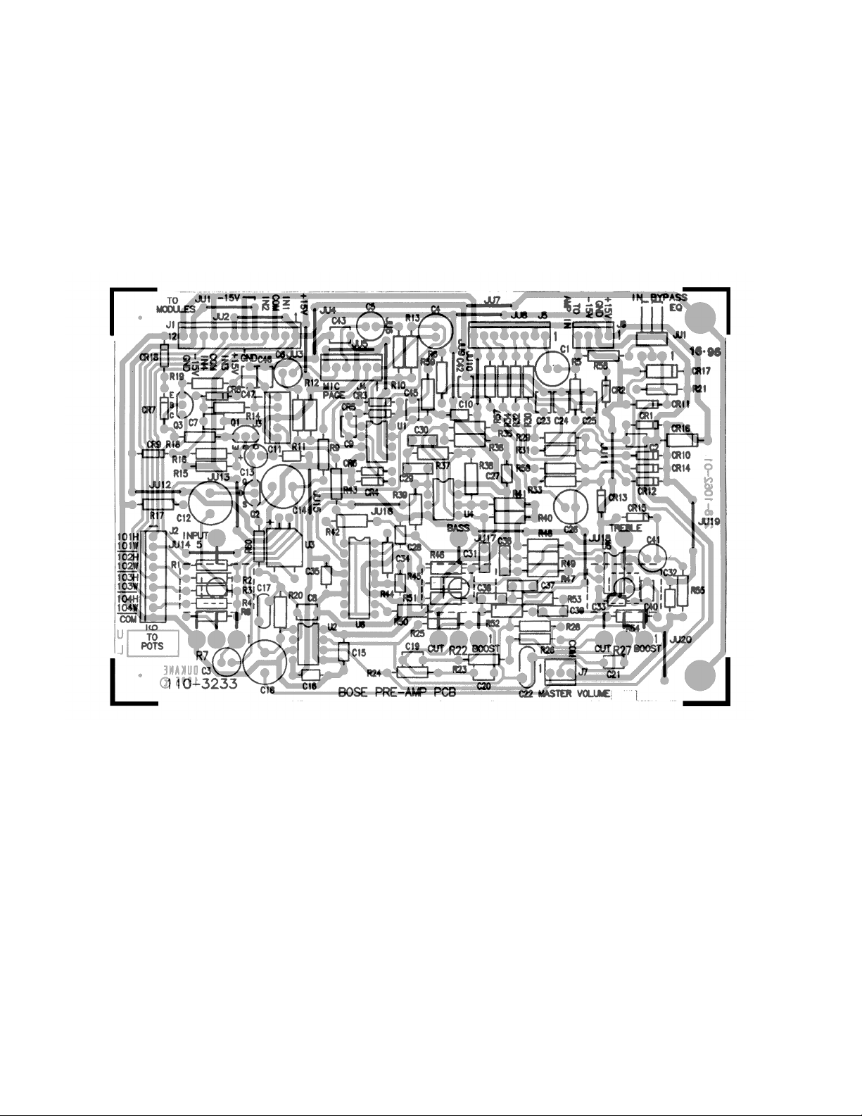
Figure 9. 230V Tone/Volume/Equalizer PCB Layout
44
Page 45

Figure 10. 230V Wiring Diagram
(Part 1)
45
Page 46

Figure 11. 230V Wiring Diagram
(Part 2)
46
Page 47

47
Page 48

SPECIFICATIONS AND FEATURES SUBJECT TO CHANGE WITHOUT NOTICE
®
®
BOSE CORPORATION
THE MOUNTAIN
FRAMINGHAM, MASSACHUSETTS USA 01701
P/N 177864 3/96: REV. 0 FOR TECHNICAL ASSISTANCE OR PART ORDERS, CALL 1 -800 -367 -4008
Page 49

FREESPACE® BUSINESS MUSIC AMPLIFIER
BMA-125
120/230V
®
120V Version shown
©1996 Bose Corporation
Service Manual
Part Number 177864
 Loading...