

Page 1

Contents
Safety Information.............................................................................................................................2
Electrostatic Discharge Sensitive (ESDS) Device Handling..........................................................3
Theory of Operation ...................................................................................................................... 5-8
Figure 1. Block Diagram....................................................................................................................8
Disassembly/Assembly Procedures .......................................................................................... 9-11
Test Setup Procedure .....................................................................................................................12
®
Test Procedures ................................................................................................................ 13-15
402
®
802
Test Procedures ................................................................................................................ 16-18
Part List Notes .................................................................................................................................19
Figure 2. 402, 802 II Original Version Exploded View .....................................................................20
Figure 3. 402, 802 II Current Version Exploded View ......................................................................20
Main Part List............................................................................................................................. 21-22
402 Electrical Part List .............................................................................................................. 23-28
802 II Electrical Part List .......................................................................................................... 29-35
402 II Electrical Part List .......................................................................................................... 36-42
802 III Electrical Part List......................................................................................................... 43-48
402 and 802 II Electrical Part List ............................................................................................ 49-50
Packaging Part List .........................................................................................................................51
Figure 4. Packaging Exploded View................................................................................................51
Frequency Response Curves................................................................................................... 52-64
PROPRIETARY INFORMATION
THIS DOCUMENT CONTAINS PROPRIETARY INFORMATION OF
BOSE
®
CORPORATION WHICH IS BEING FURNISHED ONLY FOR THE
PURPOSE OF SERVICING THE IDENTIFIED BOSE PRODUCT BY AN
AUTHORIZED BOSE SERVICE CENTER OR OWNER OF THE BOSE
PRODUCT, AND SHALL NOT BE REPRODUCED OR USED FOR ANY
OTHER PURPOSE.
1
Page 2

SAFETY INFORMATION
1. Parts that have special safety characteristics are identified by the symbol on
schematics or by special notes on the parts list. Use only replacement parts that
have critical characteristics recommended by the manufacturer.
2. Make leakage current or resistance measurements to determine that exposed
parts are acceptably insulated from the supply circuit before returning the unit
to the customer. Refer to Paragraph 84 of UL 1270. Use the following checks to
perform these measurements:
A. Leakage Current Hot Check-With the unit completely reassembled, plug
the AC line cord directly into a 120V AC outlet. (Do not use an isolation
transformer during this test.) Use a leakage current tester or a metering
system that complies with American National Standards Institute (ANSI)
C101.1 “Leakage Current for Appliances” and Underwriters Laboratories
(UL) 1492 (71). With the unit AC switch first in the ON position, then in the
OFF position, measure from a known earth ground (metal water pipe,
conduit, etc.) to all exposed metal parts of the unit (antennas, handle bracket,
metal cabinet, screwheads, metallic overlays, control shafts, etc.), especially
any exposed metal parts that offer an electrical return path to the chassis.
Any current measured must not exceed 0.5 milliamp. Reverse the unit power
cord plug in the outlet and repeat test. ANY MEASUREMENTS NOT WITHIN
THE LIMITS SPECIFIED HEREIN INDICATE A POTENTIAL SHOCK HAZ ARD THAT MUST BE ELIMINATED BEFORE RETURNING THE UNIT TO
THE CUSTOMER.
B. Insulation Resistance Test Cold Check-(1) Unplug the power supply and
connect a jumper wire between the two prongs of the plug. (2) Turn on the
power switch of the unit. (3) Measure the resistance with an ohmmeter be-
tween the jumpered AC plug and each exposed metallic cabinet part on the
unit. When the exposed metallic part has a return path to the chassis, the
reading should be between 1 and 5.2 Megohms. When there is no return path
to the chassis, the reading must be “infinite”. If it is not within the limits specified,
there is the possibility of a shock hazard, and the unit must be repaired and re checked before it is returned to the customer.
2
Page 3

ELECTROSTATIC DISCHARGE SENSITIVE (ESDS)
DEVICE HANDLING
This unit contains ESDS devices. We recommend the following precautions when repairing,
replacing, or transporting ESDS devices:
• Perform work at an electrically grounded work station.
• Wear wrist straps that connect to the station or heel straps that connect to conductive floor
mats.
• Avoid touching the leads or contacts of ESDS devices or PC boards even if properly
grounded. Handle boards by the edges only.
• Transport or store ESDS devices in ESD protective bags, bins, or totes. Do not insert unprotected devices into materials such as plastic, polystyrene foam, clear plastic bags, bubble wrap
or plastic trays.
3
Page 4

SPECIFICATIONS
Dimensions: 1.63" H x 19.0" W x 10" D (4.14 x 48.3 x 25.4 cm)
Weight: 5.5 lbs. (2.5 kg.)
Chassis material: 16 gauge steel with painted/zinc coated finish
Cover plate material: Brushed aluminum, painted
Input Connections: Balanced XLR
Output Connections: Balanced high frequency and low frequency XLR
Input Impedance: Balanced input, -10 dB level: 14 k W
Balanced input, +4 dB level: 6 k W
Unbalanced input (+ input used), -10 dB level: 12 k W
Unbalanced input (+ input used), +4 dB level: 4 k W
Output Impedance: 100 W nominal
Input Level: -10 dB or +4 dB, selectable
Output Level: 8.0 Vrms max. @ 1 kHz into 10 k W load
Low Frequency (LF)
Output Mode: Sum or normal
LF Output Level: -18 dB to +3 dB, variable
Crossover Frequency: 140 Hz (Bi-amp mode), Roll-off slope: -18 dB/oct.
Total harmonic distortion:
802: Midrange distortion of HF output:
402: Midrange distortion of HF output: < 0.2% at 1.4 V, 850 Hz
402, 802: Low frequency distortion of LF output: < 0.1 % at 160 mV, 80 Hz
Output Noise: Bi-amp mode, HF outputs: < 90µV
Bi-amp mode, LF outputs: < 40µV
Passive mode: < 90µV
< 0.2 % at 5.8 V, 700 Hz
Offset: All channels: < 15 mV
Power Requirements: 120 VAC, 50/60 Hz, 12 Watts (US/Can.)
230 VAC, 50/60 Hz, 12 Watts (Eur.)
100 VAC, 50/60 Hz, 12 Watts (Japan)
240 VAC, 50/60 Hz, 12 Watts (Aus./UK)
4
Page 5

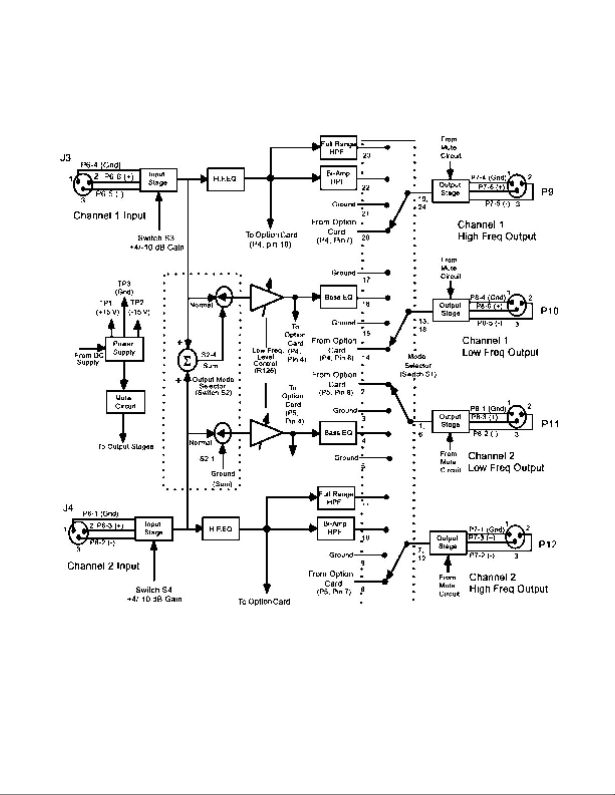
THEORY OF OPERATION
This discussion is an electrical overview of the 402® and 802® controllers. Equalization curves
are referenced and are located in the back of this manual. Additionally, the block diagram and
schematic diagrams should be referenced as required.
1. Differential Input Stage
The input stage features protection against RFI (radio frequency interference), ESD (electrostatic discharge), and overvoltage. Referring to the channel 1 circuit, R2/C1, R1/C120, R3/C2,
and R9, R10/C7 provide low pass filtering to reduce the possibility of RFI. Diodes D1-D4, D25,
and D26 provide input clamping to protect against overvoltage and ESD.
Op-amp U1 amplifies the difference between the + and - input pins, and converts it to a single
ended signal that drives the equalizers. Gain switch S3 selects between two gains, a high gain
setting for -10 dB sources and a low gain setting for +4 dB sources.
2. Equalizer for High Frequency Outputs
Op-amps U1, U2 and U3 constitute the principal equalization for the high frequency output.
Each stage makes a contribution to the total low or high frequency contouring required by the
loudspeaker. Op-amp U4 (pins 12, 13 and 14) implements a high pass filter suitable for the Full
Range mode, while op-amp U4 (pins 8, 9, and 10) is selected for a high pass filter with a higher
corner frequency for use in the Bi-amp mode. The circuitry is duplicated for both channels. See
the high frequency equalization curves for more information about the stage by stage response
of the equalizer.
3. Output mode switch, Low frequency level control, and Normal/sum mode stage
Output mode switch S2 (on the rear panel) controls op-amp summing amplifier U6 (pins 5, 6,
and 7). In the normal mode, the stage is not used, and the channel 1 and channel 2 low frequency outputs pass independent, 2-channel bass to 2 bass cabinets. In the sum mode, channels 1 and 2 are combined, and this "mono" bass signal appears at the channel 1 low frequency output only. Potentiometer R126 (on the rear panel), Low Frequency Level, provides for
adjustment of the signal sent into the low frequency equalizer.
4. Equalizer for Low Frequency Outputs
After the normal/sum stage, there is op-amp stage U7 (pins 12, 13, and 14) and op-amp equal-
izer stages U7 (pins 8, 9, and 10), U8 (pins 12, 13, and 14), and U8 (pins 8, 9, and 10). The
equalizer provides high pass, low pass, and contouring equalization. See the low frequency
equalization curves for more information about the stage by stage response of the equalizer.
5. Mode switch
Rotary switch S1 is located on the rear panel. It selects the four operating modes for the con-
trollers. Currently, position 3 (NC) is not used.
5
Page 6

THEORY OF OPERATION
6. Output stage
NOTE: The components mentioned in this paragraph are for the high frequency output only.
The output stage is compatible with balanced signal transmission systems. Inverting op-amp
stage U9 (pins 1, 2, and 3) provides the output signal. Diodes D9, D10, D29 and D30 provide
output clamping to protect against overvoltage and ESD. Relays K1 and K2 clamp the outputs
to ground to protect against power on/off transients. When the relay is de-energized, as when
the AC power is off, the outputs are clamped. About 1.2 seconds after the power is turned on,
the relay is energized by transistor Q1 and allows audio to pass through the controller. When
the power is turned off, a fast acting detector de-energizes the relays to protect against power
off transients.
NOTE: At the controller outputs, only the positive (+) output pin is driven. The negative (-)
output pin is connected to signal ground through a series impedance identical to the positive (+)
pin. When used to drive a balanced input, the controller output provides equal common-mode
source impedances (100 W). This guarantees that any common-mode noise is induced equally
into the positive (+) and negative (-) legs of a differential input in order to take full advantage of
common-mode noise rejection.
7. Power Supply
The controllers use only a nominal amount of power. Therefore, full wave bridge rectifier Z1 and
regulators U13 and U14 are all that are needed to develop the quiet, stable +/- 15 volt supply
needed by the op-amps.
8. Turn On/Off Muting Circuit
Relays K1 and K2 clamp the outputs and are controlled by three sections of quad comparator
U15. U15 (pins 8, 9 and 14) drives the relay control transistor Q1 by pulling the relay-coil terminal to nearly 15 volts . This energizes the relay for normal audio operation. At power on, U15
(pins 8, 9 and 14) is prevented from energizing the relay until capacitor C152 can be charged
up sufficiently. This takes about 1.2 seconds, and mutes any turn-on transients. At power off,
U15 (pins 2, 4, and 5) quickly detects the loss of AC power and causes Q1 to snap quickly off.
This de-energizes the relay in about 100 ms, before any transients can reach the output.
9. Troubleshooting Tips
If a differential output test generator isn't available, connect the generator ground to the
controller's ground terminal, and the generator hot lead to the negative (-) input terminal.
Leave the positive (+) terminal unconnected.
If you need to connect the controller outputs to a single-ended (not differential) instrument,
connect the controller's output ground to the instrument ground, and the controller's positive (+)
output terminal to the instrument hot pin. Leave the negative (-) output pin unconnected.
Since the controllers are two channel devices, you can troubleshoot any problem occurring in
only one channel more easily by applying the identical signal to both channel 1 and channel 2
inputs and tracing stage by stage, comparing the signal as it passes through the various
stages. In general, the corresponding channel 1 and channel 2 stages share the left and right
hand sides of the respective op-amps. This makes it easier to compare the stages.
6
Page 7

THEORY OF OPERATION
With a nominal AC power input voltage (100, 115, or 230, depending on the country), the AC
voltages at the transformer secondary should be:
between P3-1 and P3-3: 41.3 Vrms
With a cold (i.e. -room temperature) power transformer, you should expect primary and secondary resistances of:
For the 100 VAC version:
between P2-1 and P2-2: 41.8 W
between P3-1 and P3-3: 6.9 W
For the 115 VAC version:
between P2-1 and P2-2: 45.4 W
between P3-1 and P3-3: 6.3 W
For the 230/240 VAC version:
between P2-1 and P2-2: 195 W
between P3-1 and P3-3: 7.1 W
Other DC voltages are of use in troubleshooting:
Turn On/Off Muting Circuit
Typical DC voltages after 2 seconds wake up
U15-1 Section not used
U15-2 +13.5
U15-3 -15.0
U15-4 +.15
U15-5 +3.2
U15-6 Section not used
U15-7 Section not used
U15-8 +7.5
U15-9 +13.5
U15-10 +7.5
U15-11 +9.7
U15-12 -15.0
U15-13 +13.5
U15-14 -13.9
Q1-collector -14.7
Power Supply
U13-1 +26.0
U14-2 -26.0
7
Page 8
THEORY OF OPERATION
Figure 1. Block Diagram
8
Page 9

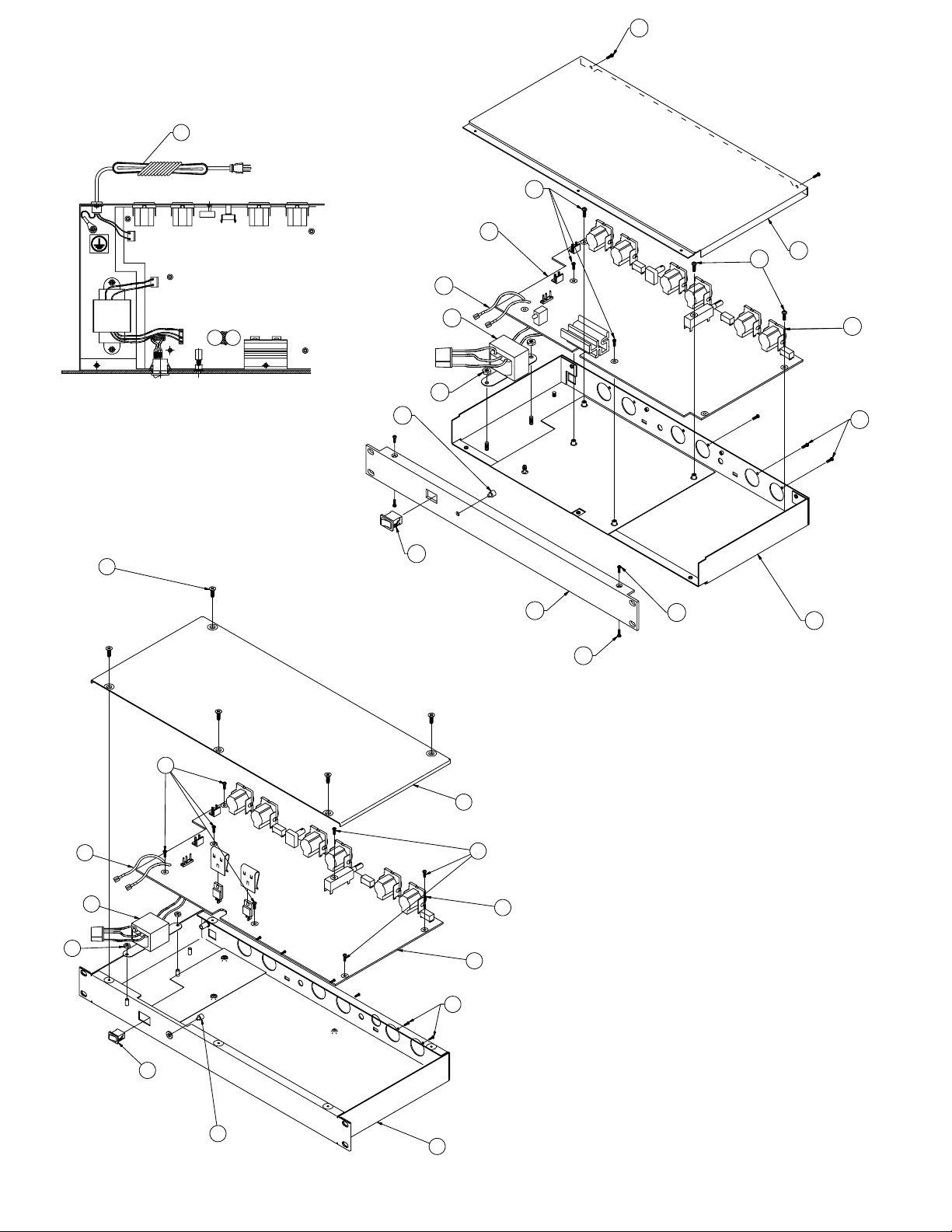
DISASSEMBLY/ASSEMBLY PROCEDURES
402® and 802® II First Variation (Removable Front Panel)
Note: Refer to Figure 2 for the following
procedures.
1. Top cover Removal
1.1 Remove the two screws (7) that secure
the top cover (2) to the front panel (9).
1.2 Remove the two screws (1) that secure
the top cover to the rear of the chassis.
1.3 Lift up the rear of the top cover and
slide it out from under the front panel.
2. Top cover Replacement
2.1 Place the top cover (2) onto the unit and
slide it under the front panel (9).
2.2 Secure the rear of the top cover using
the screws (1) removed in procedure 1.2.
2.3 Secure the front of the top cover using
the two screws (7) removed in procedure
1.1.
3. Front Panel Removal
3.1 Perform procedure 1.
3.2 Remove the two wires (14) that connect
to the power switch (10).
NOTE: On some earlier versions there was
hot melt applied to the wires.
3.3 Remove the two screws (7) that secure
the front cover to the bottom of the chassis.
3.4 Pull the front panel away from the
chassis.
4. Front Panel Replacement
4.1 Slide the front panel (9) onto the chas-
sis.
4.2 Replace the two screws (7) that secure
the front panel (9) to the bottom of the
chassis.
4.3 Connect the two wires (14) to the
power switch (10).
4.4 Perform procedure 2.
5. PCB Removal
5.1 Perform procedure 3.
5.2 Remove the 6 screws (5) that secure
the connectors (4) to the rear panel.
5.3 Disconnect the one line cord connector
(P1) and the two power transformer connectors P2) and (P3).
NOTE: If the Opti-Voice
on the PCB assembly remove the connector from the Opti-Voice PCB.
5.4 Remove the 5 screws (3) that secure
the PCB assembly (15) to the chassis.
5.5 Squeeze the two metal posts (not
shown) located at the two front corners of
the PCB and lift up the PCB. Slide the PCB
assembly towards the front of the chassis
and lift it out.
6. PCB Replacement
6.1 Slide the PCB assembly (15) into the
front of the unit aligning the connectors (4)
to the rear panel. Push the two front
corners of the PCB on to the two metal
posts.
6.2 Secure the PCB assembly to the chassis using the 5 screws (3) that were removed in procedure 5.4.
6.3 Secure the PCB to the rear panel using
the 6 screws (5) that were removed in
procedure 5.2.
6.4 Reconnect all connectors removed in
procedure 5.3.
6.5 Perform procedure 4.
®
PCB is installed
9
Page 10

DISASSEMBLY/ASSEMBLY PROCEDURES
®
402
and 802® II First Variation (Removable Front Panel)
Note: Refer to Figure 2 for the following
procedures.
7. Transformer Removal
7.1 Perform procedure 1.
7.2 Disconnect the two wire harnesses (P2)
and (P3) from the transformer to the PCB.
7.3 Remove the two 11/32” hex nuts (12)
that secure the transformer (13) to the
chassis.
7.4 Lift the transformer up and away from
the chassis.
8. Transformer Replacement
8.1 Place the transformer (13) into the
chassis aligning it to the studs.
Note: Proper orientation is required for the
transformer wire harnesses.
8.2 Secure the transformer to the chassis
using the two 11/32” hex nuts (12) that was
removed in procedure 7.3.
8.3 Connect the two wire harnesses from
the transformer to the PCB.
8.4 Perform procedure 2.
10
Page 11

DISASSEMBLY/ASSEMBLY PROCEDURES
402® and 802® II Second Variation
Note: Refer to Figure 3 for the following
procedures.
1. Top Cover Removal
1.1 Remove the 5 screws (1) that secure
the top cover (2) to the chassis.
1.2 Lift off the top cover .
2. Top Cover Replacement
2.1 Place the top cover (2) onto the chassis.
2.2 Secure the top cover to the chassis
using the 5 screws (1) that were remove in
procedure 1.1.
NOTE: The front panel is not removable.
3. PCB Removal
3.1 Perform procedure 1.
4.2 Secure the PCB assembly (5) to the
chassis using the 7 screws (3) removed in
procedure 3.4.
4.3 Secure the connectors (4) to the rear
panel using the 6 screws (6) removed in
procedure 3.3.
4.4 Connect the connectors for the line
cord and power transformer. If the
opti-Voice PCB was used, connect the
harness to the PCB.
4.5 Perform procedure 2.
5. Transformer Removal
5.1 Perform procedure 1.
5.2 Disconnect the two wire harnesses
from the transformer (11) to the PCB
assembly (5).
3.2 Disconnect the two power transformer
connectors and the two wires (12) going to
the power switch (9).
NOTE: If the opti-Voice
disconnect the harness at the opti-Voice
PCB.
3.3 Remove the 6 screws (6) that secure
the connectors (4) to the rear panel.
3.4 Remove the 7 screws (3) that secure
the PCB assembly (5) to the chassis.
3.5 Slide the PCB assembly towards the
front of the unit and lift up the rear of the
PCB to remove it from the chassis.
4. PCB Replacement
4.1 Place the PCB assembly into the
chassis aligning the connectors (4) with the
rear panel.
®
PCB is used,
5.3 Remove the two 11/32” hex nuts (10)
that secure the transformer to the chassis.
5.4 Lift the transformer up and away from
the chassis.
6. Transformer Replacement
6.1 Place the transformer (11) into the
chassis aligning it to the studs.
Note: Proper orientation is required for the
transformer wire harnesses.
6.2 Secure the transformer to the chassis
using the two 11/32” hex nuts (10) that
were removed in procedure 7.3.
6.3 Connect the two wire harnesses from
the transformer to the PCB.
6.4 Perform procedure 2.
11
Page 12
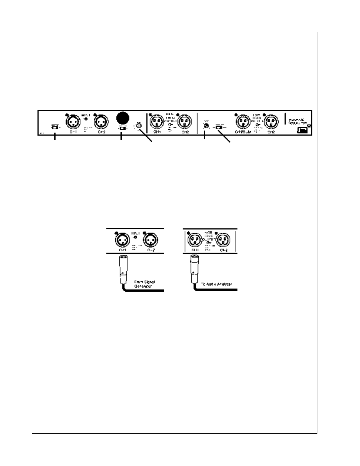
TEST SETUP PROCEDURE
The controls on the back panel should be set as follows (unless otherwise specified):
1. Set the input switches to the -10 dB position.
2. Set the Mode switch to the number 2 (BA) position.
3. Set the Low Frequency Level control to the +3 dB position.
4. Set the Output Mode switch to the NORM position
input
switch
Input connections: connect pin 1 (-) and pin 3 (shield) together at the signal generator and
audio analyzer (oscilloscope and dB meter).
input
switch
Input and Output connection Diagram
mode
switch
Back Panel View
low freq.
switch
output
mode
switch
The following test procedures refer to the 402
and the 802 series III. These references are to the PCB assembly changes that were made
recently to accommodate the new series of 402 and 802 speakers.
The new PCB assembly can be identified by the label on the top side of the PCB near the
BOSE® logo. The following are the new PCB assembly part numbers:
259148 for the 402
259145 for the 802
®
, 402 series II, 802® series II
12
Page 13
402® TEST PROCEDURES
Note: Perform the following tests on both
channels.
1. High Frequency Gain Test
1.1 Apply a 100 mVrms, 850 Hz signal to
the controller’s input terminals.
1.2 Reference a dB meter to the input of the
controller.
1.3 Measure the gain at the high frequency
output terminals. The gain should be +9.8
+ 1.0 dB.
1.4 Change the input switches to +4 dB.
1.5 The gain should be -3.4 + 1.0 dB.
2. Low Frequency Gain Test
Note: Set the input switches to the -10 dB
position.
2.1 Apply a 100 mVrms, 80 Hz signal to the
controller’s input terminals.
2.2 Reference a dB meter to the input.
2.3 Measure the gain at the low frequency
outputs. The gain should be +22.5 dB + 2.0
dB.
3.2 Reference a dB meter to the input
signal.
3.3 Measure the response at the high
frequency output terminals. Refer to the
frequency response table for the series of
402 you are testing.
402 Frequency Response Table
Full Range Mode
Frequency Output Tolerance
60 Hz -3.7 dB
105 Hz +8.5 dB
220 Hz +3.5 dB
850 Hz 0.0 dB reference
4 kHz +5.8 dB
14.5 kHz +13.3 dB
402 Series II Frequency Response Table
Full Range Mode
Frequency Output Tolerance
60 Hz +3.2 dB
90 Hz +10.0 dB
220 Hz +7.3 dB
600 Hz -2.4 dB
850 Hz 0.0 dB reference
4 kHz +5.6 dB
13.5 kHz +15.5 dB
±1.5 dB
±1.5 dB
±1.5 dB
±1.5 dB
±1.5 dB
±1.5 dB
±1.5 dB
±1.5 dB
±1.5 dB
±1.5 dB
±1.5 dB
2.4 Change the Output Mode switch to the
SUM position and measure the output at
channel 1. The gain should be +28.1 dB
+ 1.5 dB.
3. Frequency Response Test Full Range
Mode
Note: Set the Mode switch to the number 1
position (FR), the input switch to the -10 dB
position and the Output Mode switch to the
NORM position.
3.1 Apply a 100 mVrms, 850 Hz signal to
the controller’s input terminals.
4. Frequency Response Test Bi-Amp Mode
Note: Set the Mode switch to the number 2
position (BA).
4.1 Apply a 100mVrms, 850 Hz signal to
the controller’s input terminals.
4.2 Reference a dB meter to the input
signal.
4.3 Measure the output at the high frequency output terminals. Refer to the
frequency response table for the series of
402 you are testing.
13
Page 14
402® TEST PROCEDURES
402 Frequency Response Table Bi-Amp Mode
Full Range Output
Frequency Output Tolerance
60 Hz -16.4 dB
105 Hz -4.8 dB
220 Hz +2.8 dB
850 Hz 0.0 dB reference
4 kHz +5.8 dB
14.5 kHz +13.3 dB
402 Series II Frequency Response Table
Bi-Amp Mode Full Range Output
Frequency Output Tolerance
60 Hz -13.0 dB
90 Hz -5.6 dB
220 Hz +6.8 dB
600 Hz -2.4 dB
850 Hz 0.0 dB reference
4 kHz +5.8 dB
13.5 kHz +15.5 dB
5. Low Frequency Response Bi-Amp Mode
5.1 Apply a 100mVrms, 80 Hz signal to the
controller’s input terminals.
5.2 Reference a dB meter to the input.
5.3 Measure the output at the low fre-
quency output terminals. Refer to the
frequency response table for the series
of 402 you are testing.
±1.5 dB
±1.5 dB
±1.5 dB
±1.5 dB
±1.5 dB
±1.5 dB
±1.5 dB
±1.5 dB
±1.5 dB
±1.5 dB
±1.5 dB
402 Series II Low Frequency Response Table
Bi-Amp Mode Low Frequency Output
Frequency Output Tolerance
40 Hz -6.2 dB
80 Hz 0.0 dB reference
100 Hz +1.3 dB
300 Hz -17.5 dB
6. Midrange Distortion Test
Note: Set the Input Mode switch to the +4
dB position for the following test procedures.
6.1 Set the mode switch to the number 1
(FR) position.
6.2 Apply a 7.5 Vrms, 850 Hz signal to the
controller’s input.
6.3 Measure the distortion at the high
frequency output terminals. The measurement should be < .1%.
7. High Frequency Distortion Test
7.1 Apply a 2.25 Vrms, 6 kHz signal to the
controller’s input terminals.
7.2 Measure the distortion at the high
frequency output terminals. The measurement should be < .2%.
8. Low Frequency Distortion Test Bi-Amp
Mode
±2 dB
±1 dB
±2 dB
402 Low Frequency Response Table Bi-Amp
Mode Low Frequency output
Frequency Output Tolerance
40 Hz -6.2 dB
80 Hz 0.0 dB reference
100 Hz +1.3 dB
300 Hz -17.5 dB
±2 dB
±1 dB
±2 dB
8.1 Set the mode switch to the 2 (BA)
position.
8.2 Apply a 1.6 Vrms, 80 Hz signal to the
controller’s input terminals.
8.3 Measure the distortion at the low frequency output terminals. The measurement
should be < .1%.
14
Page 15

402® TEST PROCEDURES
9. Midrange Frequency Distortion Test
Bi-Amp Mode
9.1 Apply a 7.5 Vrms, 850 Hz signal to the
controller’s input terminals.
9.2 Measure the distortion at the high
frequency output terminals. The measurement should be < .1%.
10. High Frequency Distortion Test Bi-Amp
Mode
10.1 Apply a 2.25 Vrms, 6 kHz signal to the
controller’s input terminals.
10.2 Measure the distortion at the high
frequency output terminals. The measurement should be < .2%.
11. Clipping Headroom Test
11.1 Apply a 6.9 Vrms, 850 Hz signal to the
controller’s input terminals.
11.2 Measure the distortion (at an output
of 4.6
+ .5 Vrms) at the high frequency
output terminals. The measurement should
be < 1%.
12. Channel Separation Test Bi-Amp Mode
12.1 Apply a 7.5 Vrms, 850 Hz signal to the
controller’s input terminals.
12.2 Reference a dB meter to the left
channel output.
12.3 Measure the right channel output. It
should be > 40 dB.
13. Hum
13.1 Measure the hum and noise at the low
frequency outputs with no input signal
applied. The reading should be < 40 uV.
15
Page 16

802® TEST PROCEDURES
Note: Perform the following tests on both
channels.
1. High Frequency Gain Test
1.1 Apply a 100 mVrms, 700 Hz signal to
the controller’s input terminals.
1.2 Reference a dB meter to the input of the
controller.
1.3 Measure the gain at the high frequency
output terminals. The gain should be +15.1
+ 1.0 dB.
1.4 Change the input switches to +4 dB.
1.5 The gain should be 2.0 + 1.0 dB.
2. Low Frequency Gain Test
Note: Set the input switches to the -10 dB
position.
2.1 Apply a 100 mVrms, 80 Hz signal to the
controller’s input terminals.
2.2 Reference a dB meter to the input.
2.3 Measure the output at the low fre-
quency outputs. The gain should be +23.5
dB + 2.0 dB.
2.4 Change the Output Mode switch to the
SUM position and measure the output at
channel 1. The gain should be +28.1 dB
+ 1.5 dB.
3. Frequency Response Test Full Range
Mode
Note: Set the Mode switch to the number 1
position (FR), the input switch to the -10 dB
position and the Output Mode switch to the
NORM position.
3.1 Apply a 100 mVrms, 700 Hz signal to
the controller’s input terminals.
3.2 Reference a dB meter to the input
signal.
3.3 Measure the response at the high
frequency output terminals. Refer to the
frequency response table for the series of
802 you are testing.
802 Series II Frequency Response Table
Full Range Mode
Frequency Output Tolerance
40 Hz +8.0 dB
55 Hz +13.5 dB
140 Hz +6.6 dB
700 Hz 0.0 dB reference
2.5 kHz +2.1 dB
6 kHz +9.6 dB
15 kHz +16.7 dB
802 Series III Frequency Response Table
Full Range Mode
Frequency Output Tolerance
40 Hz +1.9 dB
70 Hz +13.5 dB
140 Hz +7.5 dB
700 Hz 0.0 dB reference
2.5 kHz +1.8 dB
6 kHz +6.9 dB
15 kHz +13.8 dB
4. Frequency Response Test Bi-Amp Mode
Note: Set the Mode switch to the number 2
position (BA).
4.1 Apply a 100mVrms, 700 Hz signal to
the controller’s input terminals.
4.2 Reference a dB meter to the input
signal.
±1.5 dB
±1.5 dB
±1.5 dB
±1.5 dB
±1.5 dB
±1.5 dB
±1.5 dB
±1.5 dB
±1.5 dB
±1.5 dB
±1.5 dB
±1.5 dB
16
4.3 Measure the output at the high fre-
quency output terminals. Refer to the
frequency response table for the series of
802 you are testing.
Page 17
802® TEST PROCEDURES
802 Series II Frequency Response Table
Bi-Amp Mode Full Range Output
Frequency Output Tolerance
40 Hz -21.0 dB
60 Hz -11.5 dB
700 Hz 0.0 dB reference
2.5 kHz +2.1 dB
6 kHz +9.6 dB
15 kHz +16.7 dB
802 Series III Frequency Response Table
Bi-Amp Mode Full Range Output
Frequency Output Tolerance
40 Hz -24.9 dB
70 Hz -10.6 dB
140 Hz +5.2 dB
700 Hz 0.0 dB reference
2.5 kHz +1.9 dB
6 kHz +7.0 dB
13 kHz +13.9 dB
±1.5 dB
±1.5 dB
±1.5 dB
±1.5 dB
±1.5 dB
±1.5 dB
±1.5 dB
±1.5 dB
±1.5 dB
±1.5 dB
±1.5 dB
802 Series III Low Frequency Response Table
Bi-Amp Mode Low Frequency output
Frequency Output Tolerance
40 Hz -6.2 dB
2 dB
±
80 Hz 0.0 dB reference
100 Hz +1.3 dB
300 Hz -17.5 dB
Note: Set the Input Mode switch to the +4
dB position for the following test procedures.
6. Midrange Distortion Test
6.1 Set the mode switch to the number 1
(FR) position.
6.2 Apply a 5.8 Vrms, 700 Hz signal to the
controller’s input.
6.3 Measure the distortion at the high
frequency output terminals. The measurement should be
< .2%.
1.5 dB
±
2 dB
±
5. Low Frequency Response Bi-Amp Mode
5.1 Apply a 100mVrms, 80 Hz signal to the
controller’s input terminals.
5.2 Reference a dB meter to the input.
5.3 Measure the output at the low fre-
quency output terminals. Refer to the
frequency response table for the series
802 you are testing.
802 Series II Low Frequency Response Table
Bi-Amp Mode Low Frequency output
Frequency Output Tolerance
40 Hz -6.2 dB
80 Hz 0.0 dB reference
100 Hz +1.3 dB
300 Hz -17.5 dB
±2 dB
±1.5 dB
±2 dB
7. High Frequency Distortion Test
7.1 Apply a 1.30 Vrms, 6 kHz signal to the
controller’s input terminals.
7.2 Measure the distortion at the high
frequency output terminals. The measurement should be < .2%.
8. Low Frequency Distortion Test Bi-Amp
Mode
8.1 Set the mode switch to the number 2
(BA) position.
8.2 Apply a 1.6 Vrms, 80 Hz signal to the
controller’s input terminals.
8.3 Measure the distortion at the low frequency output terminals. The measurement
should be < .1%.
17
Page 18

802® TEST PROCEDURES
9. Midrange Frequency Distortion Test
Bi-Amp Mode
9.1 Apply a 5.8 Vrms, 700 Hz signal to the
controller’s input terminals.
9.2 Measure the distortion at the high
frequency output terminals. The measurement should be
10. High Frequency Distortion Test Bi-Amp
Mode
10.1 Apply a 1.30Vrms, 6 kHz signal to the
controller’s input terminals.
10.2 Measure the distortion at the high
frequency output terminals. The measurement should be < .2%.
< .1%.
11. Clipping Headroom Test
11.1 Apply a 5.8 Vrms, 700 Hz signal to the
controller’s input terminals.
11.2 Measure the distortion (at an output of
7.35 + .5 Vrms) at the high frequency
output terminals. The measurement should
be < .1%.
12. Channel Separation Test Bi-Amp Mode
12.1 Apply a 4.0 Vrms, 700 Hz signal to the
controller’s input terminals.
12.2 Measure the channel separation
across the high frequency output terminals.
It should be > 40 dB.
13. Hum
13.1 Measure the hum and noise at the low
frequency outputs with no input signal
applied. The reading should be < 40 uV.
18
Page 19

PART LIST NOTES
1. This part is not normally available from customer service. Approval from the Field Service
Manager is required before ordering.
2. The individual parts located on the PCBs are listed in the Electrical Part List.
3. This part is critical for safety purposes. Failure to use a substitute replacement with the
same safety characteristics as the recommended replacement part might create shock, fire
and/or other hazards.
4. This part is not shown.
19
Page 20
16
14
15
1
(2x)
3
2
3
(6x)
11
12
13
(2x)
4
5
(6x)
10
1
(5x)
9
8
(2x)
7
(2x)
6
Figure 2. 402®, 802® II Original
Version Exploded View
3
10
12
2x
11
2
2x
3
7x
4
Figure 3. 402, 802 II Current Version
5
6
6X
9
8
7
Exploded View
20
Page 21
MAIN PART LIST
See Figure 2
Item
Number
1 SCREW, TAPP, #4-40 x .375, PAN, XREC 170284-06 2
2 COVER, CHASSIS, EQ, CNTLR 172180 1
3 SCREW, TAPP, #4-40 x .25, PAN, TORX 171796-04 5
4 CONNECTOR, XLR, MALE
CONNECTOR, XLR, FEMALE
5 SCREW, TAPP, #4-40 x .375, PAN, XREC 170284-06 6
6 CHASSIS, EQ, CONTROLLER 173002-03 1
7 SCREW, TAPP, #4-40 x .312, BTN, XREC 170285-05 2
8 SCREW, TAPP, #4-40 x .312, BTN, XREC 170285-05 2
9 FRONT PANEL, ASSEMBLY 172181 1
10 SWITCH, ROCKER, SPST, POWER 143960 1 3
11 LENS, LED, CHASSIS, CLEAR 144023 1
12 STND. HEX NUT, WASHER, KEPS 118260-08 3
13 TRANSFORMER, 100/120V
TRANSFORMER, 220/230V
Description Part Number Qty. Note
144004
189222-001
180128-1
180128-2
4
2
13
15
16 LINE CORD, 3 WIRE, USA/CAN
PCB ASSY, CONTROLLER. 402C
PCB ASSY, CONTROLLER, 802C
LINE CORD, 2 WIRE, 220V, EURO
LINE CORD, 2 WIRE, 100V, JAPAN
LINE CORD, 3 WIRE, 230V, UK
LINE CORD, 2 WIRE, 240V, AUST.
II
III
259145
259148
173242
173243
173244
173245
173246
1 1, 4
13
21
Page 22

MAIN PART LIST
See Figure 3
Item
Number
1 SCREW, 6-32 x .5, TAPP, FLAT, XREC 198422-008 5
2 COVER, CHASSIS, EQ, CNTLR 198374-001 1
3 SCREW, TAPP, 4-40 x .25, PAN, XREC 103118-04 7
4 CONNECTOR, XLR, MALE
CONNECTOR, XLR, FEMALE
5
6 SCREW, TAPP, #4-40 x .375, PAN, XREC 170284-06 6
7 CHASSIS, EQ, CONTROLLER 198373-005 1
8 LENS, LED, CHASSIS, CLEAR 144023 1
9 SWITCH, ROCKER, SPST, POWER 143960 1 3
10 STND. HEX NUT, WASHER, KEPS 118260-08 3
11 TRANSFORMER, 100/120V
PCB ASSY., CONTROLLER. 402C II
PCB ASSY., CONTROLLER, 802C III
TRANSFORMER, 220/230V
Description Part Number Qty. Note
144004
189222-001
259145
259148
180128-1
180128-2
4
2
11
13
16 LINE CORD, 3 WIRE, USA/CAN
LINE CORD, 2 WIRE, 220V, EURO
LINE CORD, 2 WIRE, 100V, JAPAN
LINE CORD, 3 WIRE, 230V, UK
LINE CORD, 2 WIRE, 240V, AUST.
173242
173243
173244
173245
173246
13
22
Page 23

402® ELECTRICAL PART LIST
Resistors
Reference Designator Description Part Number Note
R1 1.00K, 1206, 1/8W, 1% 124894-1001
R2 1.00K, MF, 1% 121245-2211001
R3 1.00K, MF, 1% 121245-2211001
R4 1.00K, 1206, 1/8W, 1% 124894-1001
R5 100K, CF, 2% 121243-1211042
R6 100K, CF, 2% 121243-1211042
R7 2.00K, 1206, 1/8W, 1% 124894-2001
R8 8.06K, 1206, 1/8W, 1% 124894-8061
R9 8.06K, 1206, 1/8W, 1% 124894-8061
R10 2.00K, 1206, 1/8W, 1% 124894-2001
R11 10.0K, 1206, 1/8W, 1% 124894-1002
R12 10.0K, 1206, 1/8W, 1% 124894-1002
R13 3.92K, 1206, 1/8W, 1% 124894-3921
R14 3.92K, 1206, 1/8W, 1% 124894-3921
R17 JUMPER, CHIP 124896
R19 JUMPER, CHIP 124896
R21 JUMPER, CHIP 124896
R24 JUMPER, CHIP 124896
R27 JUMPER, CHIP 124896
R30 JUMPER, CHIP 124896
R32 274K, 1206, 1/8W, 1% 124894-2743
R33 20K, 1206, 1/8W, 1% 124894-2002
R36 78.7K, 1206, 1/8W, 1% 124894-7872
R37 21.5K, 1206, 1/8W, 1% 124894-2152
R38 6.81K, 1206, 1/8W, 1% 124894-6811
R39 6.81K, 1206, 1/8W, 1% 124894-6811
R40 4.75K, 1206, 1/8W, 1% 124894-4751
R41 5.90K, 1206, 1/8W, 1% 124894-5901
R42 5.11K, 1206, 1/8W, 1% 124894-5111
R43 221K, 1206, 1/8W, 1% 124894-2213
R44 1.10K, 1206, 1/8W, 1% 124894-1101
R45 49.9K, 1206, 1/8W, 1% 124894-4992
R46 68.1K, 1206, 1/8W, 1% 124894-6812
R47 6.98K, 1206, 1/8W, 1% 124894-6981
R48 5.49K, 1206, 1/8W, 1% 124894-5491
R49 14.0K, 1206, 1/8W, 1% 124894-1402
R50 14.0K, 1206, 1/8W, 1% 124894-1402
R64 JUMPER, CHIP 124896
R65 1.00K, 1206, 1/8W, 1% 124894-1001
R66 1.00K, MF, 1% 121245-2211001
R67 1.00K, MF, 1% 121245-2211001
R68 1.00K, 1206, 1/8W, 1% 124894-1001
R69 2.00K, 1206, 1/8W, 1% 124894-2001
R70 8.06K, 1206, 1/8W, 1% 124894-8061
R71 8.06K, 1206, 1/8W, 1% 124894-8061
R72 2.00K, 1206, 1/8W, 1% 124894-2001
R73 10.0K, 1206, 1/8W, 1% 124894-1002
23
Page 24

402® ELECTRICAL PART LIST
Resistors (continued)
Reference Designator Description Part Number Note
R74 10.0K, 1206, 1/8W, 1% 124894-1002
R75 3.92K, 1206, 1/8W, 1% 124894-3921
R76 3.92K, 1206, 1/8W, 1% 124894-3921
R79 JUMPER, CHIP 124896
R81 JUMPER, CHIP 124896
R83 JUMPER, CHIP 124896
R86 JUMPER, CHIP 124896
R89 JUMPER, CHIP 124896
R92 JUMPER, CHIP 124896
R94 274K, 1206, 1/8W, 1% 124894-2743
R95 20K, 1206, 1/8W, 1% 124894-2002
R98 78.7K, 1206, 1/8W, 1% 124894-7872
R99 21.5K, 1206, 1/8W, 1% 124894-2152
R100 4.75K, 1206, 1/8W, 1% 124894-4751
R101 5.90K, 1206, 1/8W, 1% 124894-5901
R102 5.11K, 1206, 1/8W, 1% 124894-5111
R103 221K, 1206, 1/8W, 1% 124894-2213
R104 1.10K, 1206, 1/8W, 1% 124894-1101
R105 49.9K, 1206, 1/8W, 1% 124894-4992
R106 68.1K, 1206, 1/8W, 1% 124894-6812
R107 6.98K, 1206, 1/8W, 1% 124894-6981
R108 5.49K, 1206, 1/8W, 1% 124894-5491
R109 14.0K, 1206, 1/8W, 1% 124894-1402
R110 14.0K, 1206, 1/8W, 1% 124894-1402
R113 JUMPER, CHIP 124896
R117 JUMPER, CHIP 124896
R120 JUMPER, CHIP 124896
R125 JUMPER, CHIP 124896
R127 5.6K, CF, 5%, .5W, 52mm 121243-1515625
R128 100K, CF, 2%, 52mm 121243-1211042
R129 100K, CF, 2%, 52mm 121243-1211042
R130 2.74K, 1206, 1/8W, 1% 124894-2741
R131 4.75K, 1206, 1/8W, 1% 124894-4751
R134 4.75K, 1206, 1/8W, 1% 124894-4751
R135 4.75K, 1206, 1/8W, 1% 124894-4751
R136 JUMPER, CHIP 124896
R138 2.74K, 1206, 1/8W, 1% 124894-2741
R139 4.75K, 1206, 1/8W, 1% 124894-4751
R142 4.75K, 1206, 1/8W, 1% 124894-4751
R143 4.75K, 1206, 1/8W, 1% 124894-4751
R144 JUMPER, CHIP 124896
R146 47 OHM, MF, 1/4W, 2%, 52mm 121243-1214702
R147 47 OHM, MF, 1/4W, 2%, 52mm 121243-1214702
R148 47 OHM, MF, 1/4W, 2%, 52mm 121243-1214702
R149 47 OHM, MF, 1/4W, 2%, 52mm 121243-1214702
R150 47 OHM, MF, 1/4W, 2%, 52mm 121243-1214702
R151 47 OHM, MF, 1/4W, 2%, 52mm 121243-1214702
24
Page 25

402® ELECTRICAL PART LIST
Resistors (continued)
Reference Designator Description Part Number Note
R152 47 OHM, MF, 1/4W, 2% 121243-1214702
R153 47 OHM, MF, 1/4W, 2% 121243-1214702
R154 4.75K, 1206, 1/8W, 1% 124894-4751
R155 4.75K, 1206, 1/8W, 1% 124894-4751
R156 JUMPER, CHIP 124896
R157 10K, CF, 5%, .5W 121243-1511035
R158 47.5K, 1206, 1/8W, 1% 124894-4752
R159 47.5K, 1206, 1/8W, 1% 124894-4752
R160 1.00K, 1206, 1/8W, 1% 124894-1001
R161 4.32K, 1206, 1/8W, 1% 124894-4321
R162 8.25K, 1206, 1/8W, 1% 124894-8251
R163 1.82K, 1206, 1/8W, 1% 124894-1821
R164 1.82K, 1206, 1/8W, 1% 124894-1821
R167 1.00K, 1206, 1/8W, 1% 124894-1001
R168 4.32K, 1206, 1/8W, 1% 124894-4321
R169 8.25K, 1206, 1/8W, 1% 124894-8251
R170 1.82K, 1206, 1/8W, 1% 124894-1821
R171 1.82K, 1206, 1/8W, 1% 124894-1821
R174 681 OHM, 1206, 1/8W, 1% 124894-6810
R175 681 OHM, 1206, 1/8W, 1% 124894-6810
R176 681 OHM, 1206, 1/8W, 1% 124894-6810
R177 681 OHM, 1206, 1/8W, 1% 124894-6810
R180 221K, 1206, 1/8W, 1% 124894-2213
R182 JUMPER, CHIP 124896
R183 221K, 1206, 1/8W, 1% 124894-2213
R184 100K, 1206, 1/8W, 1% 124894-1003
R185 100K, 1206, 1/8W, 1% 124894-1003
R191 47.5 OHM, 1206, 1/8W, 1% 124894-47R5
R192 47.5 OHM, 1206, 1/8W, 1% 124894-47R5
R193 47 OHM, MF, 1/4W, 2% 121243-1214702
R194 47 OHM, MF, 1/4W, 2% 121243-1214702
R195 47.5 OHM, 1206, 1/8W, 1% 124894-47R5
R196 47.5 OHM, 1206, 1/8W, 1% 124894-47R5
R197 47.5 OHM, 1206, 1/8W, 1% 124894-47R5
R198 47.5 OHM, 1206, 1/8W, 1% 124894-47R5
R199 6.81K, 1206, 1/8W, 1% 124894-6811
R200 10.0K, 1206, 1/8W, 1% 124894-1002
R201 17.8K, 1206, 1/8W, 1% 124894-1782
R202 1 MEG, 1206, 1/8W, 5% 124895-1055
R203 221 OHM, 1206, 1/8W, 1% 124894-2210
R204 221 OHM, 1206, 1/8W, 1% 124894-2210
R205 47.5K, 1206, 1/8W, 1% 124894-4752
R206 1 MEG, 1206, 1/8W, 5% 124895-1055
R207 47.5K, 1206, 1/8W, 1% 124894-4752
R208 10.0K, 1206, 1/8W, 1% 124894-1002
R209 47.5K, 1206, 1/8W, 1% 124894-4752
R210 475 OHM, 1206, 1/8W, 1% 124894-4750
R212 4.75K, 1206, 1/8W, 1% 124894-4751
25
Page 26

402® ELECTRICAL PART LIST
Capacitors
Reference Designator Description Part Number Note
C1 1000pF, 1206, COG, 50V, 10% 124956-1022
C2 1000pF, 1206, COG, 50V, 10% 124956-1022
C3 22uF, EL, 85C, 35V, 50% 119944-220
C4 22uF, EL, 85C, 35V, 50% 119944-220
C5 .1uF, 1206, Y5V, 50V, 80% 138551-104
C6 .1uF, 1206, Y5V, 50V, 80% 138551-104
C7 100pF, 1206, COG, 50V, 10% 124956-1012
C8 100pF, 1206, COG, 50V, 10% 124956-1012
C9 0.27uF, BOX, 85, 100V, 5% 137127-274
C10 680pF, SL, DISC, 50V, 10% 137269-681
C12 .047uF, BOX, 85, 50V, 5% 137127-473
C13 JUMPER, 0 OHM 139942
C16 .1uF, 1206, Y5V, 50V, 80% 138551-104
C17 .1uF, 1206, Y5V, 50V, 80% 138551-104
C22 JUMPER, 0 OHM 139942
C23 .022uF, BOX, 85, 100V, 5% 137127-223
C24 .022uF, BOX, 85, 100V, 5% 137127-223
C25 JUMPER, 0 OHM 139942
C26 .022uF, BOX, 85, 100V, 5% 137127-223
C27 .022uF, BOX, 85, 100V, 5% 137127-223
C28 .47uF, BOX, 85, 50V, 5% 137127-474
C29 .22uF, BOX, 85, 50V, 5% 137127-224
C30 .22uF, BOX, 85, 50V, 5% 137127-224
C31 .1uF, BOX, 85, 50V, 5% 137127-104
C32 .1uF, BOX, 85, 50V, 5% 137127-104
C33 .22uF, BOX, 85, 50V, 5% 137127-224
C34 .022uF, BOX, 85, 100V, 5% 137127-223
C35 .18uF, BOX, 85, 50V, 5% 137127-184
C36 .1uF, 1206, Y5V, 50V, 80% 138551-104
C37 .1uF, 1206, Y5V, 50V, 80% 138551-104
C47 1000pF, 1206, COG, 50V, 10% 124956-1022
C48 1000pF, 1206, COG, 50V, 10% 124956-1022
C49 22uF, EL, 85, 35V, 50% 119944-220
C50 22uF, EL, 85, 35V, 50% 119944-220
C51 .1uF, 1206, Y5V, 50V, 80% 138551-104
C52 .1uF, 1206, Y5V, 50V, 80% 138551-104
C55 100pF, 1206, COG, 50V, 10% 124956-1012
C56 100pF, 1206, COG, 50V, 10% 124956-1012
C57 0.27uF, BOX, 85, 100V, 5% 137127-274
C58 680pF, SL, DISC, 50V, 10% 137269-681
C60 .047uF, BOX, 85, 50V, 5% 137127-473
C61 JUMPER, 0 OHM 139942
C64 .1uF, 1206, Y5V, 50V, 80% 138551-104
C65 .1uF, 1206, Y5V, 50V, 80% 138551-104
C70 JUMPER, 0 OHM 139942
C71 .022uF, BOX, 85, 100V, 5% 137127-223
26
Page 27

402® ELECTRICAL PART LIST
Capacitors (continued)
Reference Designator Description Part Number Note
C72 .022uF, BOX, 85, 100V, 5% 137127-223
C73 JUMPER, 0 OHM 139942
C74 .022uF, BOX, 85, 100V, 5% 137127-223
C75 .022uF, BOX, 85, 100V, 5% 137127-223
C76 .1uF, 1206, Y5V, 50V, 80% 138551-104
C77 .1uF, 1206, Y5V, 50V, 80% 138551-104
C78 .47uF, BOX, 85, 50V, 5% 137127-474
C79 .22uF, BOX, 85, 50V, 5% 137127-224
C80 .22uF, BOX, 85, 50V, 5% 137127-224
C81 .1uF, BOX, 85, 50V, 5% 137127-104
C82 .1uF, BOX, 85, 50V, 5% 137127-104
C83 .22uF, BOX, 85, 50V, 5% 137127-224
C84 .022uF, BOX, 85, 100V, 5% 137127-223
C85 .18uF, BOX, 85, 50V, 5% 137127-184
C86 .1uF, 1206, Y5V, 50V, 80% 138551-104
C87 .1uF, 1206, Y5V, 50V, 80% 138551-104
C97 .1uF, 1206, Y5V, 50V, 80% 138551-104
C98 .1uF, 1206, Y5V, 50V, 80% 138551-104
C99 .1uF, 1206, Y5V, 50V, 80% 138551-104
C100 .1uF, 1206, Y5V, 50V, 80% 138551-104
C101 100pF, 1206, COG, 50V, 10% 124956-1012
C103 100pF, 1206, COG, 50V, 10% 124956-1012
C105 100pF, 1206, COG, 50V, 10% 124956-1012
C107 100pF, 1206, COG, 50V, 10% 124956-1012
C109 .0047uF, 250VAC, 20% 146354 3
C110 .01uF, 1206, Y5V, 50V, 80% 124959-103
C111 .01uF, 1206, Y5V, 50V, 80% 124959-103
C112 .01uF, 1206, Y5V, 50V, 80% 124959-103
C113 2200uF, EL, 105C, 50V, 20% 144000-222H 3
C114 2200uF, EL, 105C, 50V, 20% 144000-222H 3
C115 1uF, EL, 85C, 35V, 50% 137265-1R0
C116 1uF, EL, 85C, 35V, 50% 137265-1R0
C117 1uF, EL, 85C, 35V, 50% 137265-1R0
C118 1uF, EL, 85C, 35V, 50% 137265-1R0
C119 100pF, 1206, COG, 50V, 10% 124956-1012
C120 100pF, 1206, COG, 50V, 10% 124956-1012
C121 0.0047uF, BOX, 85, 100V, 5% 137127-472
C122 0.0022uF, BOX, 85, 100V, 5% 137127-222
C123 .047uF, BOX, 85, 50V, 5% 137127-473
27
Page 28

402® ELECTRICAL PART LIST
Capacitors (continued)
Reference Designator Description Part Number Note
C125 0.0047uF, BOX, 85, 100V, 5% 137127-472
C126 0.0022uF, BOX, 85, 100V, 5% 137127-222
C127 .047uF, BOX, 85, 50V, 5% 137127-473
C129 .1uF, 1206, Y5V, 50V, 80% 138551-104
C130 .1uF, 1206, Y5V, 50V, 80% 138551-104
C131 .1uF, 1206, Y5V, 50V, 80% 138551-104
C132 .1uF, 1206, Y5V, 50V, 80% 138551-104
C133 .01uF, 1206, Y5V, 50V, 80% 124959-103
C140 .1uF, BOX, 85, 50V, 5% 137127-104
C141 .1uF, BOX, 85, 50V, 5% 137127-104
C142 1000pF, 1206, COG, 50V, 10% 124956-1022
C143 1000pF, 1206, COG, 50V, 10% 124956-1022
C144 1000pF, 1206, COG, 50V, 10% 124956-1022
C145 1000pF, 1206, COG, 50V, 10% 124956-1022
C146 1000pF, 1206, COG, 50V, 10% 124956-1022
C147 1000pF, 1206, COG, 50V, 10% 124956-1022
C148 1000pF, 1206, COG, 50V, 10% 124956-1022
C149 1000pF, 1206, COG, 50V, 10% 124956-1022
C150 .1uF, 1206, Y5V, 50V, 80% 138551-104
C151 .1uF, 1206, Y5V, 50V, 80% 138551-104
C152 22uF, EL, BP, 85C, 25V, 20% 147522-220
C153 22uF, EL, 85C, 35V, 50% 119944-220
C155 22uF, EL, 85C, 35V, 50% 119944-220
C157 22uF, EL, 85C, 35V, 50% 119944-220
C159 22uF, EL, 85C, 35V, 50% 119944-220
C161 .1uF, 1206, Y5V, 50V, 80% 138551-104
C162 100pF, 1206, COG, 50V, 10% 124956-1012
C163 100pF, 1206, COG, 50V, 10% 124956-1012
C164 100pF, 1206, COG, 50V, 10% 124956-1012
28
Page 29

802® II ELECTRICAL PART LIST
Resistors
Reference Designator Description Part Number Note
R1 1.00K, 1206, 1/8W, 1% 124894-1001
R2 1.00K, MF, 1% 121245-2211001
R3 1.00K, MF, 1% 121245-2211001
R4 1.00K, 1206, 1/8W, 1% 124894-1001
R5 100K, CF, 2% 121243-1211042
R6 100K, CF, 2% 121243-1211042
R7 2.00K, 1206, 1/8W, 1% 124894-2001
R8 8.06K, 1206, 1/8W, 1% 124894-8061
R9 8.06K, 1206, 1/8W, 1% 124894-8061
R10 2.00K, 1206, 1/8W, 1% 124894-2001
R11 13K, 1206, 1/8W, 1% 124894-1302
R12 1.00K, 1206, 1/8W, 1% 124894-1001
R13 18K, 1206, 1/8W, 1% 124894-1835
R14 18K, 1206, 1/8W, 1% 124894-1835
R15 20K, 1206, 1/8W, 1% 124894-2002
R16 2.74K, 1206, 1/8W, 1% 124894-2741
R17 JUMPER, CHIP 124896
R18 9.09K, 1206, 1/8W, 1% 124894-9091
R19 JUMPER, CHIP 124896
R21 JUMPER, CHIP 124896
R24 JUMPER, CHIP 124896
R25 2.00K, 1206, 1/8W, 1% 124894-2001
R26 470 OHM, 1206, 1/8W, 5% 124895-4715
R27 22K, 1206, 1/8W, 1% 124894-2235
R28 27.4K, 1206, 1/8W, 1% 124894-2742
R29 130K, 1206, 1/8W, 1% 124894-1303
R30 8.2K, 1206, 1/8W, 1% 124894-8225
R31 2.00K, 1206, 1/8W, 1% 124894-2001
R32 160K, 1206, 1/8W, 1% 124894-1645
R33 6.81K, 1206, 1/8W, 1% 124894-6811
R34 10.0K, 1206, 1/8W, 1% 124894-1002
R35 1.74K, 1206, 1/8W, 1% 124894-1741
R36 34.8K, 1206, 1/8W, 1% 124894-3482
R37 2.00K, 1206, 1/8W, 1% 124894-2001
R38 6.81K, 1206, 1/8W, 1% 124894-6811
R39 6.81K, 1206, 1/8W, 1% 124894-6811
R40 4.75K, 1206, 1/8W, 1% 124894-4751
R41 5.90K, 1206, 1/8W, 1% 124894-5901
R42 5.11K, 1206, 1/8W, 1% 124894-5111
R43 221K, 1206, 1/8W, 1% 124894-2213
R44 1.10K, 1206, 1/8W, 1% 124894-1101
R45 49.9K, 1206, 1/8W, 1% 124894-4992
R46 68.1K, 1206, 1/8W, 1% 124894-6812
R47 6.98K, 1206, 1/8W, 1% 124894-6981
R48 5.49K, 1206, 1/8W, 1% 124894-5491
R49 14.0K, 1206, 1/8W, 1% 124894-1402
R50 14.0K, 1206, 1/8W, 1% 124894-1402
29
Page 30

802® II ELECTRICAL PART LIST
Resistors (continued)
Reference Designator Description Part Number Note
R64 JUMPER, CHIP 124896
R65 1.00K, 1206, 1/8W, 1% 124894-1001
R66 1.00K, MF, 1% 121245-2211001
R67 1.00K, MF, 1% 121245-2211001
R68 1.00K, 1206, 1/8W, 1% 124894-1001
R69 2.00K, 1206, 1/8W, 1% 124894-2001
R70 8.06K, 1206, 1/8W, 1% 124894-8061
R71 8.06K, 1206, 1/8W, 1% 124894-8061
R72 2.00K, 1206, 1/8W, 1% 124894-2001
R73 13K, 1206, 1/8W, 1% 124894-1302
R74 1.00K, 1206, 1/8W, 1% 124894-1001
R75 18K, 1206, 1/8W, 1% 124894-1835
R76 18K, 1206, 1/8W, 1% 124894-1835
R77 20K, 1206, 1/8W, 1% 124894-2002
R78 2.74K, 1206, 1/8W, 1% 124894-2741
R79 JUMPER, CHIP 124896
R80 9.09K, 1206, 1/8W, 1% 124894-9091
R81 JUMPER, CHIP 124896
R83 JUMPER, CHIP 124896
R85 2.49K, 1206, 1/8W, 1% 124894-2491
R86 JUMPER, CHIP 124896
R87 2.00K, 1206, 1/8W, 1% 124894-2001
R88 470 OHM, 1206, 1/8W, 5% 124895-4715
R89 22K, 1206, 1/8W, 1% 124894-2235
R90 27.4K, 1206, 1/8W, 1% 124894-2742
R91 130K, 1206, 1/8W, 1% 124894-1303
R92 8.2K, 1206, 1/8W, 1% 124894-8225
R93 2.00K, 1206, 1/8W, 1% 124894-2001
R94 160K, 1206, 1/8W, 1% 124894-1645
R95 6.81K, 1206, 1/8W, 1% 124894-6811
R96 10.0K, 1206, 1/8W, 1% 124894-1002
R97 1.74K, 1206, 1/8W, 1% 124894-1741
R98 34.8K, 1206, 1/8W, 1% 124894-3482
R99 2.00K, 1206, 1/8W, 1% 124894-2001
R100 4.75K, 1206, 1/8W, 1% 124894-4751
R101 5.90K, 1206, 1/8W, 1% 124894-5901
R102 5.11K, 1206, 1/8W, 1% 124894-5111
R103 221K, 1206, 1/8W, 1% 124894-2213
R104 1.10K, 1206, 1/8W, 1% 124894-1101
R105 49.9K, 1206, 1/8W, 1% 124894-4992
R106 68.1K, 1206, 1/8W, 1% 124894-6812
R107 6.98K, 1206, 1/8W, 1% 124894-6981
R108 5.49K, 1206, 1/8W, 1% 124894-5491
R109 14.0K, 1206, 1/8W, 1% 124894-1402
R110 14.0K, 1206, 1/8W, 1% 124894-1402
R113 JUMPER, CHIP 124896
30
Page 31

802® II ELECTRICAL PART LIST
Resistors (continued)
Reference Designator Description Part Number Note
R117 JUMPER, CHIP 124896
R120 JUMPER, CHIP 124896
R125 JUMPER, CHIP 124896
R127 5.6K, CF, 5%, .5W 121243-1515625
R128 100K, CF, 2% 121243-1211042
R129 100K, CF, 2% 121243-1211042
R130 4.75K, 1206, 1/8W, 1% 124894-4751
R131 4.75K, 1206, 1/8W, 1% 124894-4751
R134 4.75K, 1206, 1/8W, 1% 124894-4751
R135 4.75K, 1206, 1/8W, 1% 124894-4751
R136 JUMPER, CHIP 124896
R138 4.75K, 1206, 1/8W, 1% 124894-4751
R139 4.75K, 1206, 1/8W, 1% 124894-4751
R142 4.75K, 1206, 1/8W, 1% 124894-4751
R143 4.75K, 1206, 1/8W, 1% 124894-4751
R144 JUMPER, CHIP 124896
R146 47 OHM, MF, 1/4W, 2% 121243-1214702
R147 47 OHM, MF, 1/4W, 2% 121243-1214702
R148 47 OHM, MF, 1/4W, 2% 121243-1214702
R149 47 OHM, MF, 1/4W, 2% 121243-1214702
R150 47 OHM, MF, 1/4W, 2% 121243-1214702
R151 47 OHM, MF, 1/4W, 2% 121243-1214702
R152 47 OHM, MF, 1/4W, 2% 121243-1214702
R153 47 OHM, MF, 1/4W, 2% 121243-1214702
R154 4.75K, 1206, 1/8W, 1% 124894-4751
R155 4.75K, 1206, 1/8W, 1% 124894-4751
R156 JUMPER, CHIP 124896
R157 10K, CF, 5%, .5W 121243-1511035
R158 47.5K, 1206, 1/8W, 1% 124894-4752
R159 47.5K, 1206, 1/8W, 1% 124894-4752
R160 1.00K, 1206, 1/8W, 1% 124894-1001
R161 4.32K, 1206, 1/8W, 1% 124894-4321
R162 JUMPER, CHIP 124896
R165 23.7K, 1206, 1/8W, 1% 124894-2372
R166 61.9K, 1206, 1/8W, 1% 124894-6192
R167 1.00K, 1206, 1/8W, 1% 124894-1001
R168 4.32K, 1206, 1/8W, 1% 124894-4321
R169 JUMPER, CHIP 124896
R172 23.7K, 1206, 1/8W, 1% 124894-2372
R173 61.9K, 1206, 1/8W, 1% 124894-6192
R174 681 OHM, 1206, 1/8W, 1% 124894-6810
R175 681 OHM, 1206, 1/8W, 1% 124894-6810
R176 681 OHM, 1206, 1/8W, 1% 124894-6810
R177 681 OHM, 1206, 1/8W, 1% 124894-6810
R180 221K, 1206, 1/8W, 1% 124894-2213
R182 JUMPER, CHIP 124896
31
Page 32

802® II ELECTRICAL PART LIST
Resistors (continued)
Reference Designator Description Part Number Note
R183 221K, 1206, 1/8W, 1% 124894-2213
R191 47.5 OHM, 1206, 1/8W, 1% 124894-47R5
R192 47.5 OHM, 1206, 1/8W, 1% 124894-47R5
R193 47 OHM, MF, 1/4W, 2%, 52mm 121243-1214702
R194 47 OHM, MF, 1/4W, 2%, 52mm 121243-1214702
R195 47.5 OHM, 1206, 1/8W, 1% 124894-47R5
R196 47.5 OHM, 1206, 1/8W, 1% 124894-47R5
R197 47.5 OHM, 1206, 1/8W, 1% 124894-47R5
R198 47.5 OHM, 1206, 1/8W, 1% 124894-47R5
R199 6.81K, 1206, 1/8W, 1% 124894-6811
R200 10.0K, 1206, 1/8W, 1% 124894-1002
R201 17.8K, 1206, 1/8W, 1% 124894-1782
R202 1 MEG, 1206, 1/8W, 5% 124895-1055
R203 221 OHM, 1206, 1/8W, 1% 124894-2210
R204 221 OHM, 1206, 1/8W, 1% 124894-2210
R205 47.5K, 1206, 1/8W, 1% 124894-4752
R206 1 MEG, 1206, 1/8W, 5% 124895-1055
R207 47.5K, 1206, 1/8W, 1% 124894-4752
R208 10.0K, 1206, 1/8W, 1% 124894-1002
R209 47.5K, 1206, 1/8W, 1% 124894-4752
R210 475 OHM, 1206, 1/8W, 1% 124894-4750
R212 4.75K, 1206, 1/8W, 1% 124894-4751
Capacitors
Reference Designator Description Part Number Note
C1 1000pF, 1206, COG, 50V, 10% 124956-1022
C2 1000pF, 1206, COG, 50V, 10% 124956-1022
C3 22uF, EL, 85C, 35V, 50% 119944-220
C4 22uF, EL, 85C, 35V, 50% 119944-220
C5 .1uF, 1206, Y5V, 50V, 80% 138551-104
C6 .1uF, 1206, Y5V, 50V, 80% 138551-104
C7 100pF, 1206, COG, 50V, 10% 124956-1012
C8 100pF, 1206, COG, 50V, 10% 124956-1012
C9 .0068uF, BOX, 85, 100V, 5% 137127-682
C10 270pF, SL, DISC, 50V, 10% 137269-271
C11 .0012uF, BOX, 85, 63V, 5% 137127-122
C12 .0068uF, BOX, 85, 100V, 5% 137127-682
C13 .0068uF, BOX, 85, 100V, 5% 137127-682
C14 .0082uF, BOX, 85, 100V, 5% 137127-822
C15 .0056uF, BOX, 85, 100V, 5% 137127-562
C16 .1uF, 1206, Y5V, 50V, 80% 138551-104
C17 .1uF, 1206, Y5V, 50V, 80% 138551-104
C18 .033uF, BOX, 85, 100V, 5% 137127-333
C19 .068uF, BOX, 85, 100V, 5% 137127-683
C20 .033uF, BOX, 85, 100V, 5% 137127-333
C22 .1uF, BOX, 85, 50V, 5% 137127-104
C23 .1uF, BOX, 85, 50V, 5% 137127-104
32
Page 33

802® II ELECTRICAL PART LIST
Capacitors (continued)
Reference Designator Description Part Number Note
C24 .33uF, BOX, 85, 100V, 5% 137127-334
C25 .15uF, BOX, 85, 50V, 5% 137127-154
C26 .15uF, BOX, 85, 50V, 5% 137127-154
C27 .47uF, BOX, 85, 50V, 5% 137127-474
C28 .47uF, BOX, 85, 50V, 5% 137127-474
C29 .22uF, BOX, 85, 50V, 5% 137127-224
C30 .22uF, BOX, 85, 50V, 5% 137127-224
C31 .1uF, BOX, 85, 50V, 5% 137127-104
C32 .1uF, BOX, 85, 50V, 5% 137127-104
C33 .22uF, BOX, 85, 50V, 5% 137127-224
C34 .022uF, BOX, 85, 100V, 5% 137127-223
C35 .18uF, BOX, 85, 50V, 5% 137127-184
C36 .1uF, 1206, Y5V, 50V, 80% 138551-104
C37 .1uF, 1206, Y5V, 50V, 80% 138551-104
C47 1000pF, 1206, COG, 50V, 10% 124956-1022
C48 1000pF, 1206, COG, 50V, 10% 124956-1022
C49 22uF, EL, 85C, 35V, 50% 119944-220
C50 22uF, EL, 85C, 35V, 50% 119944-220
C51 .1uF, 1206, Y5V, 50V, 80% 138551-104
C52 .1uF, 1206, Y5V, 50V, 80% 138551-104
C53 .1uF, 1206, Y5V, 50V, 80% 138551-104
C54 .1uF, 1206, Y5V, 50V, 80% 138551-104
C55 100pF, 1206, COG, 50V, 10% 124956-1012
C56 100pF, 1206, COG, 50V, 10% 124956-1012
C57 .0068uF, BOX, 85, 100V, 5% 137127-682
C58 270pF, SL, DISC, 50V, 10% 137269-271
C59 .0012uF, BOX, 85, 63V, 5% 137127-122
C60 .0068uF, BOX, 85, 100V, 5% 137127-682
C61 .0068uF, BOX, 85, 100V, 5% 137127-682
C62 .0082uF, BOX, 85, 100V, 5% 137127-822
C63 .0056uF, BOX, 85, 100V, 5% 137127-562
C64 .1uF, 1206, Y5V, 50V, 80% 138551-104
C65 .1uF, 1206, Y5V, 50V, 80% 138551-104
C66 .033uF, BOX, 85, 100V, 5% 137127-333
C67 .068uF, BOX, 85, 100V, 5% 137127-683
C68 .033uF, BOX, 85, 100V, 5% 137127-333
C69 100pF, 1206, COG, 50V, 10% 124956-1012
C70 .1uF, BOX, 85, 50V, 5% 137127-104
C71 .1uF, BOX, 85, 50V, 5% 137127-104
C72 .33uF, BOX, 85, 100V, 5% 137127-334
C73 .15uF, BOX, 85, 50V, 5% 137127-154
C74 .15uF, BOX, 85, 50V, 5% 137127-154
C75 .47uF, BOX, 85, 50V, 5% 137127-474
C76 .1uF, 1206, Y5V, 50V, 80% 138551-104
C77 .1uF, 1206, Y5V, 50V, 80% 138551-104
C78 .47uF, BOX, 85, 50V, 5% 137127-474
33
Page 34

802® II ELECTRICAL PART LIST
Capacitors (continued)
Reference Designator Description Part Number Note
C79 .22uF, BOX, 85, 50V, 5% 137127-224
C80 .22uF, BOX, 85, 50V, 5% 137127-224
C81 .1uF, BOX, 85, 50V, 5% 137127-104
C82 .1uF, BOX, 85, 50V, 5% 137127-104
C83 .22uF, BOX, 85, 50V, 5% 137127-224
C84 .022uF, BOX, 85, 100V, 5% 137127-223
C85 .18uF, BOX, 85, 50V, 5% 137127-184
C86 .1uF, 1206, Y5V, 50V, 80% 138551-104
C87 .1uF, 1206, Y5V, 50V, 80% 138551-104
C95 JUMPER, 0 OHM 139942
C97 .1uF, 1206, Y5V, 50V, 80% 138551-104
C98 .1uF, 1206, Y5V, 50V, 80% 138551-104
C99 .1uF, 1206, Y5V, 50V, 80% 138551-104
C100 .1uF, 1206, Y5V, 50V, 80% 138551-104
C101 100pF, 1206, COG, 50V, 10% 124956-1012
C103 100pF, 1206, COG, 50V, 10% 124956-1012
C105 100pF, 1206, COG, 50V, 10% 124956-1012
C107 100pF, 1206, COG, 50V, 10% 124956-1012
C109 .0047uF, 250VAC, 20% 146354 3
C110 .01uF, 1206, Y5V, 50V, 80% 124959-103
C111 .001uF, 1206, Y5V, 50V, 80% 124959-102
C112 .01uF, CHIP, 5% 124959-103
C113 2200uF, EL, 105C, 50V, 20% 144000-222H 3
C114 2200uF, EL, 105C, 50V, 20% 144000-222H 3
C115 1uF, EL, 85C, 35V, 50% 137265-1R0
C116 1uF, EL, 85C, 35V, 50% 137265-1R0
C117 1uF, EL, 85C, 35V, 50% 137265-1R0
C118 1uF, EL, 85C, 35V, 50% 137265-1R0
C119 100pF, 1206, COG, 50V, 10% 124956-1012
C120 100pF, 1206, COG, 50V, 10% 124956-1012
C129 .1uF, 1206, Y5V, 50V, 80% 138551-104
C130 .1uF, 1206, Y5V, 50V, 80% 138551-104
C131 .1uF, 1206, Y5V, 50V, 80% 138551-104
C132 .1uF, 1206, Y5V, 50V, 80% 138551-104
C133 1000pF, CHIP, 5% 124959-103
C142 1000pF, 1206, COG, 50V, 10% 124956-1022
C143 1000pF, 1206, COG, 50V, 10% 124956-1022
C144 1000pF, 1206, COG, 50V, 10% 124956-1022
C145 1000pF, 1206, COG, 50V, 10% 124956-1022
C146 1000pF, 1206, COG, 50V, 10% 124956-1022
34
Page 35

802® II ELECTRICAL PART LIST
Capacitors (continued)
Reference Designator Description Part Number Note
C147 1000pF, 1206, COG, 50V, 10% 124956-1022
C148 1000pF, 1206, COG, 50V, 10% 124956-1022
C149 1000pF, 1206, COG, 50V, 10% 124956-1022
C150 .1uF, 1206, Y5V, 50V, 80% 138551-104
C151 .1uF, 1206, Y5V, 50V, 80% 138551-104
C152 22uF, EL, BP, 85C, 25V, 20% 147522-220
C153 22uF, EL, 85C, 35V, 50% 119944-220
C155 22uF, EL, 85C, 35V, 50% 119944-220
C157 22uF, EL, 85C, 35V, 50% 119944-220
C159 22uF, EL, 85C, 35V, 50% 119944-220
C161 .1uF, 1206, Y5V, 50V, 80% 138551-104
C162 100pF, 1206, COG, 50V, 10% 124956-1012
C163 100pF, 1206, COG, 50V, 10% 124956-1012
C164 100pF, 1206, COG, 50V, 10% 124956-1012
35
Page 36

402® II ELECTRICAL PART LIST
Resistors
Reference Designator Description Part Number Note
R1 1.00K, 1206, 1/8W, 1% 124894-1001
R2 1.00K, MF, 1%, 52mm 121245-2211001
R3 1.00K, MF, 1%, 52mm 121245-2211001
R4 1.00K, 1206, 1/8W, 1% 124894-1001
R5 100K, CF, 2%, 52mm 121243-1211042
R6 100K, CF, 2%, 52mm 121243-1211042
R7 2.00K, 1206, 1/8W, 1% 124894-2001
R8 8.06K, 1206, 1/8W, 1% 124894-8061
R9 8.06K, 1206, 1/8W, 1% 124894-8061
R10 2.00K, 1206, 1/8W, 1% 124894-2001
R11 10.0K, 1206, 1/8W, 1% 124894-1002
R12 1.00K, 1206, 1/8W, 1% 124894-1001
R13 2.21K, 1206, 1/8W, 1% 124894-2211
R14 1.47K, 1206, 1/8W, 1% 124894-1471
R15 182K, 1206, 1/8W, 1% 124894-1823
R16 3.83K, 1206, 1/8W, 1% 124894-3831
R17 1.00K, 1206, 1/8W, 1% 124894-1001
R18 5.76K, 1206, 1/8W, 1% 124894-5761
R19 2.00K, 1206, 1/8W, 1% 124894-2001
R20 10.0K, 1206, 1/8W, 1% 124894-1002
R21 JUMPER, CHIP 124896
R24 JUMPER, CHIP 124896
R25 JUMPER, CHIP 124896
R27 30.1K, 1206, 1/8W, 1% 124894-3012
R28 5.76K, 1206, 1/8W, 1% 124894-5761
R29 2.00K, 1206, 1/8W, 1% 124894-2001
R30 634 OHM, 1206, 1/8W, 1% 124894-6340
R31 3.01K, 1206, 1/8W, 1% 124894-3011
R32 75.0K, 1206, 1/8W, 1% 124894-7502
R33 7.15K, 1206, 1/8W, 1% 124894-7151
R36 78.7K, 1206, 1/8W, 1% 124894-7872
R37 21.5K, 1206, 1/8W, 1% 124894-2152
R38 6.81K, 1206, 1/8W, 1% 124894-6811
R39 6.81K, 1206, 1/8W, 1% 124894-6811
R40 4.75K, 1206, 1/8W, 1% 124894-4751
R41 5.90K, 1206, 1/8W, 1% 124894-5901
R42 5.11K, 1206, 1/8W, 1% 124894-5111
R43 221K, 1206, 1/8W, 1% 124894-2213
R44 1.10K, 1206, 1/8W, 1% 124894-1101
R45 49.9K, 1206, 1/8W, 1% 124894-4992
R46 68.1K, 1206, 1/8W, 1% 124894-6812
R47 6.98K, 1206, 1/8W, 1% 124894-6981
R48 5.49K, 1206, 1/8W, 1% 124894-5491
R49 14.0K, 1206, 1/8W, 1% 124894-1402
R50 14.0K, 1206, 1/8W, 1% 124894-1402
R64 JUMPER, CHIP 124896
R65 1.00K, 1206, 1/8W, 1% 124894-1001
36
Page 37

402® II ELECTRICAL PART LIST
Resistors (continued)
Reference Designator Description Part Number Note
R66 1.00K, MF, 1%, 52mm 121245-2211001
R67 1.00K, MF, 1%, 52mm 121245-2211001
R68 1.00K, 1206, 1/8W, 1% 124894-1001
R69 2.00K, 1206, 1/8W, 1% 124894-2001
R70 8.06K, 1206, 1/8W, 1% 124894-8061
R71 8.06K, 1206, 1/8W, 1% 124894-8061
R72 2.00K, 1206, 1/8W, 1% 124894-2001
R73 10.0K, 1206, 1/8W, 1% 124894-1002
R74 1.00K, 1206, 1/8W, 1% 124894-1001
R76 1.47K, 1206, 1/8W, 1% 124894-1471
R75 2.21K, 1206, 1/8W, 1% 124894-2211
R77 182K, 1206, 1/8W, 1% 124894-1823
R78 3.83K, 1206, 1/8W, 1% 124894-3831
R79 1.00K, 1206, 1/8W, 1% 124894-1001
R80 5.76K, 1206, 1/8W, 1% 124894-5761
R81 2.00K, 1206, 1/8W, 1% 124894-2001
R82 10.0K, 1206, 1/8W, 1% 124894-1002
R83 JUMPER, CHIP 124896
R86 JUMPER, CHIP 124896
R87 JUMPER, CHIP 124896
R89 30.1K, 1206, 1/8W, 1% 124894-3012
R90 5.76K, 1206, 1/8W, 1% 124894-5761
R91 2.00K, 1206, 1/8W, 1% 124894-2001
R92 634 OHM, 1206, 1/8W, 1% 124894-6340
R93 3.01K, 1206, 1/8W, 1% 124894-3011
R94 75.0K, 1206, 1/8W, 1% 124894-7502
R98 78.7K, 1206, 1/8W, 1% 124894-7872
R99 21.5K, 1206, 1/8W, 1% 124894-2152
R100 4.75K, 1206, 1/8W, 1% 124894-4751
R101 5.90K, 1206, 1/8W, 1% 124894-5901
R102 5.11K, 1206, 1/8W, 1% 124894-5111
R103 221K, 1206, 1/8W, 1% 124894-2213
R104 1.10K, 1206, 1/8W, 1% 124894-1101
R105 49.9K, 1206, 1/8W, 1% 124894-4992
R106 68.1K, 1206, 1/8W, 1% 124894-6812
R107 6.98K, 1206, 1/8W, 1% 124894-6981
R108 5.49K, 1206, 1/8W, 1% 124894-5491
R109 14.0K, 1206, 1/8W, 1% 124894-1402
R110 14.0K, 1206, 1/8W, 1% 124894-1402
R113 JUMPER, CHIP 124896
R117 JUMPER, CHIP 124896
R120 JUMPER, CHIP 124896
R125 JUMPER, CHIP 124896
R127 5.6K, CF, 5%, .5W, 52mm 121243-1515625
R126 100K, CF, 2%, 52mm 121243-1211042
R129 100K, CF, 2%, 52mm 121243-1211042
R130 4.75K, 1206, 1/8W, 1% 124894-4751
37
Page 38

402® II ELECTRICAL PART LIST
Resistors (continued)
Reference Designator Description Part Number Note
R131 4.75K, 1206, 1/8W, 1% 124894-4751
R134 4.75K, 1206, 1/8W, 1% 124894-4751
R135 4.75K, 1206, 1/8W, 1% 124894-4751
R136 JUMPER, CHIP 124896
R138 4.75K, 1206, 1/8W, 1% 124894-4751
R139 4.75K, 1206, 1/8W, 1% 124894-4751
R142 4.75K, 1206, 1/8W, 1% 124894-4751
R143 4.75K, 1206, 1/8W, 1% 124894-4751
R144 JUMPER, CHIP 124896
R146 200 OHM, MF, 1/4W, 1%, 52mm 121245-2212000
R147 200 OHM, MF, 1/4W, 1%, 52mm 121245-2212000
R148 200 OHM, MF, 1/4W, 1%, 52mm 121245-2212000
R149 200 OHM, MF, 1/4W, 1%, 52mm 121245-2212000
R150 200 OHM, MF, 1/4W, 1%, 52mm 121245-2212000
R151 200 OHM, MF, 1/4W, 1%, 52mm 121245-2212000
R152 200 OHM, MF, 1/4W, 1%, 52mm 121245-2212000
R153 200 OHM, MF, 1/4W, 1%, 52mm 121245-2212000
R154 4.75K, 1206, 1/8W, 1% 124894-4751
R155 4.75K, 1206, 1/8W, 1% 124894-4751
R156 JUMPER, CHIP 124896
R157 10K, CF, 5%, .5W, 52mm 121243-1511035
R158 47.5K, 1206, 1/8W, 1% 124894-4752
R159 47.5K, 1206, 1/8W, 1% 124894-4752
R160 1.00K, 1206, 1/8W, 1% 124894-1001
R161 4.32K, 1206, 1/8W, 1% 124894-4321
R162 JUMPER, CHIP 124896
R165 25.5K, 1206, 1/8W, 1% 124894-2552
R167 1.00K, 1206, 1/8W, 1% 124894-1001
R168 4.32K, 1206, 1/8W, 1% 124894-4321
R169 JUMPER, CHIP 124896
R172 25.5K, 1206, 1/8W, 1% 124894-2552
R174 681 OHM, 1206, 1/8W, 1% 124894-6810
R175 681 OHM, 1206, 1/8W, 1% 124894-6810
R176 681 OHM, 1206, 1/8W, 1% 124894-6810
R177 681 OHM, 1206, 1/8W, 1% 124894-6810
R180 221K, 1206, 1/8W, 1% 124894-2213
R182 JUMPER, CHIP 124896
R183 221K, 1206, 1/8W, 1% 124894-2213
R191 200 OHM, CHIP, 1% 124894-2000
R192 200 OHM, CHIP, 1% 124894-2000
R193 200 OHM, MF, 1/4W, 1%, 52mm 121245-2212000
R194 200 OHM, MF, 1/4W, 1%, 52mm 121245-2212000
R195 200 OHM, CHIP, 1% 124894-2000
R196 200 OHM, CHIP, 1% 124894-2000
R197 200 OHM, CHIP, 1% 124894-2000
R198 200 OHM, CHIP, 1% 124894-2000
R199 6.81K, 1206, 1/8W, 1% 124894-6811
38
Page 39

402® II ELECTRICAL PART LIST
Resistors (continued)
Reference Designator Description Part Number Note
R200 10.0K, 1206, 1/8W, 1% 124894-1002
R201 17.8K, 1206, 1/8W, 1% 124894-1782
R202 1 MEG, 1206, 1/8W, 5% 124895-1055
R203 221 OHM, 1206, 1/8W, 1% 124894-2210
R204 221 OHM, 1206, 1/8W, 1% 124894-2210
R205 47.5K, 1206, 1/8W, 1% 124894-4752
R206 1 MEG, 1206, 1/8W, 5% 124895-1055
R207 47.5K, 1206, 1/8W, 1% 124894-4752
R208 10.0K, 1206, 1/8W, 1% 124894-1002
R209 47.5K, 1206, 1/8W, 1% 124894-4752
R210 475 OHM, 1206, 1/8W, 1% 124894-4750
R212 4.75K, 1206, 1/8W, 1% 124894-4751
R213 JUMPER, 22AWG, NON-INSUL,
10.0mm
R214 JUMPER, 22AWG, NON-INSUL,
10.0mm
R215 JUMPER, 22AWG, NON-INSUL,
10.0mm
R216 JUMPER, 22AWG, NON-INSUL,
10.0mm
R217 JUMPER, 22AWG, NON-INSUL,
10.0mm
R218 JUMPER, 22AWG, NON-INSUL,
10.0mm
148242-100
148242-100
148242-100
148242-100
148242-100
148242-100
39
Page 40

402® II ELECTRICAL PART LIST
Capacitors
Reference Designator Description Part Number Note
C1 1000pF, 1206, COG, 50V, 10% 124956-1022
C2 1000pF, 1206, COG, 50V, 10% 124956-1022
C3 22uF, EL, 85C, 35V, 50% 119944-220
C4 22uF, EL, 85C, 35V, 50% 119944-220
C5 .1uF, 1206, Y5V, 50V, 80% 138551-104
C6 .1uF, 1206, Y5V, 50V, 80% 138551-104
C7 100pF, 1206, COG, 50V, 10% 124956-1012
C9 .0022uF, BOX, 85, 100V, 5% 137127-222
C10 .0018uF, BOX, 85, 100V, 5% 137127-182
C11 .027uF, BOX, 85, 63V, 5% 137127-273
C12 .082uF, BOX, 85, 50V, 5% 137127-823
C13 .01uF, BOX, 85, 100V, 5% 137127-103
C16 .1uF, 1206, Y5V, 50V, 80% 138551-104
C17 .1uF, 1206, Y5V, 50V, 80% 138551-104
C18 .022uF, BOX, 85, 100V, 5% 137127-223
C20 .068uF, BOX, 85, 63V, 5% 137127-683
C21 .047uF, 1206, X7R, 50V, 10% 138552-473
C22 JUMPER, 0 OHM 139942
C23 .082uF, BOX, 85, 50V, 5% 137127-823
C24 .082uF, BOX, 85, 50V, 5% 137127-823
C25 JUMPER, 0 OHM 139942
C26 .022uF, BOX, 85, 100V, 5% 137127-223
C27 .022uF, BOX, 85, 100V, 5% 137127-223
C28 .47uF, BOX, 85, 50V, 5% 137127-474
C29 .22uF, BOX, 85, 50V, 5% 137127-224
C30 .22uF, BOX, 85, 50V, 5% 137127-224
C31 .1uF, BOX, 85, 50V, 5% 137127-104
C32 .1uF, BOX, 85, 50V, 5% 137127-104
C33 .22uF, BOX, 85, 50V, 5% 137127-224
C34 .022uF, BOX, 85, 100V, 5% 137127-223
C35 .18uF, BOX, 85, 50V, 5% 137127-184
C36 .1uF, 1206, Y5V, 50V, 80% 138551-104
C37 .1uF, 1206, Y5V, 50V, 80% 138551-104
C47 1000pF, 1206, COG, 50V, 10% 124956-1022
C48 1000pF, 1206, COG, 50V, 10% 124956-1022
C49 22uF, EL, 85C, 35V, 50% 119944-220
C50 22uF, EL, 85C, 35V, 50% 119944-220
C51 .1uF, 1206, Y5V, 50V, 80% 138551-104
C52 .1uF, 1206, Y5V, 50V, 80% 138551-104
C53 .1uF, 1206, Y5V, 50V, 80% 138551-104
C54 .1uF, 1206, Y5V, 50V, 80% 138551-104
C55 100pF, 1206, COG, 50V, 10% 124956-1012
C57 .0022uF, BOX, 85, 100V, 5% 137127-222
C58 .0018uF, BOX, 85, 100V, 5% 137127-182
C59 .027uF, BOX, 85, 63V, 5% 137127-273
C60 .082uF, BOX, 85, 50V, 5% 137127-823
40
Page 41

402® II ELECTRICAL PART LIST
Capacitors (continued)
Reference Designator Description Part Number Note
C61 .01uF, BOX, 85, 100V, 5% 137127-103
C64 .1uF, 1206, Y5V, 50V, 80% 138551-104
C65 .1uF, 1206, Y5V, 50V, 80% 138551-104
C66 .022uF, BOX, 85, 100V, 5% 137127-223
C68 .068uF, BOX, 85, 63V, 5% 137127-683
C69 .047uF, 1206, X7R, 50V, 10% 138552-473
C70 JUMPER, 0 OHM 139942
C71 .082uF, BOX, 85, 50V, 5% 137127-823
C72 .082uF, BOX, 85, 50V, 5% 137127-823
C73 JUMPER, 0 OHM 139942
C74 .022uF, BOX, 85, 100V, 5% 137127-223
C75 .022uF, BOX, 85, 100V, 5% 137127-223
C76 .1uF, 1206, Y5V, 50V, 80% 138551-104
C77 .1uF, 1206, Y5V, 50V, 80% 138551-104
C78 .47uF, BOX, 85, 50V, 5% 137127-474
C79 .22uF, BOX, 85, 50V, 5% 137127-224
C80 .22uF, BOX, 85, 50V, 5% 137127-224
C81 .1uF, BOX, 85, 50V, 5% 137127-104
C82 .1uF, BOX, 85, 50V, 5% 137127-104
C83 .22uF, BOX, 85, 50V, 5% 137127-224
C84 .022uF, BOX, 85, 100V, 5% 137127-223
C85 .18uF, BOX, 85, 50V, 5% 137127-184
C86 .1uF, 1206, Y5V, 50V, 80% 138551-104
C87 .1uF, 1206, Y5V, 50V, 80% 138551-104
C95 JUMPER, 0 OHM 139942
C97 .1uF, 1206, Y5V, 50V, 80% 138551-104
C98 .1uF, 1206, Y5V, 50V, 80% 138551-104
C99 .1uF, 1206, Y5V, 50V, 80% 138551-104
C100 .1uF, 1206, Y5V, 50V, 80% 138551-104
C109 .0047uF, 250VAC, 20% 146354 3
C110 .001uF, 1206, Y5V, 50V, 80% 124959-102
C111 .001uF, 1206, Y5V, 50V, 80% 124959-102
C112 .01uF, 1206, Y5V, 50V, 80% 124959-103
C113 2200uF, EL, 105C, 50V, 20% 144000-222H 3
C114 2200uF, EL, 105C, 50V, 20% 144000-222H 3
C115 1uF, EL, 85C, 35V, 50% 137265-1R0
C116 1uF, EL, 85C, 35V, 50% 137265-1R0
C117 1uF, EL, 85C, 35V, 50% 137265-1R0
C118 1uF, EL, 85C, 35V, 50% 137265-1R0
C119 100pF, 1206, COG, 50V, 10% 124956-1012
C120 100pF, 1206, COG, 50V, 10% 124956-1012
41
Page 42

402® II ELECTRICAL PART LIST
Capacitors (continued)
Reference Designator Description Part Number Note
C133 .01uF, 1206, Y5V, 50V, 80% 124959-103
C142 1000pF, 1206, COG, 50V, 10% 124956-1022
C143 1000pF, 1206, COG, 50V, 10% 124956-1022
C144 1000pF, 1206, COG, 50V, 10% 124956-1022
C145 1000pF, 1206, COG, 50V, 10% 124956-1022
C146 1000pF, 1206, COG, 50V, 10% 124956-1022
C147 1000pF, 1206, COG, 50V, 10% 124956-1022
C148 1000pF, 1206, COG, 50V, 10% 124956-1022
C149 1000pF, 1206, COG, 50V, 10% 124956-1022
C150 .1uF, 1206, Y5V, 50V, 80% 138551-104
C151 .1uF, 1206, Y5V, 50V, 80% 138551-104
C152 22uF, EL, BP, 85C, 25V, 20% 147522-220
C153 22uF, EL, 85C, 35V, 50% 119944-220
C155 22uF, EL, 85C, 35V, 50% 119944-220
C157 22uF, EL, 85C, 35V, 50% 119944-220
C159 22uF, EL, 85C, 35V, 50% 119944-220
C161 .1uF, 1206, Y5V, 50V, 80% 138551-104
C162 100pF, 1206, COG, 50V, 10% 124956-1012
C163 100pF, 1206, COG, 50V, 10% 124956-1012
C164 100pF, 1206, COG, 50V, 10% 124956-1012
42
Page 43

802® III ELECTRICAL PART LIST
Resistors
Reference Designator Description Part Number Note
R1 1.00K, 1206, 1/8W, 1% 124894-1001
R2 1.00K, MF, 1%, 52mm 121245-2211001
R3 1.00K, MF, 1%, 52mm 121245-2211001
R4 1.00K, 1206, 1/8W, 1% 124894-1001
R5 100K, CF, 2%, 52mm 121243-1211042
R6 100K, CF, 2%, 52mm 121243-1211042
R7 2.00K, 1206, 1/8W, 1% 124894-2001
R8 8.06K, 1206, 1/8W, 1% 124894-8061
R9 8.06K, 1206, 1/8W, 1% 124894-8061
R10 2.00K, 1206, 1/8W, 1% 124894-2001
R11 3.32K, 1206, 1/8W, 1% 124894-3321
R12 1.00K, 1206, 1/8W, 1% 124894-1001
R13 1.27K, 1206, 1/8W, 1% 124894-1271
R14 1.27K, 1206, 1/8W, 1% 124894-1271
R15 9.09K, 1206, 1/8W, 1% 124894-9091
R16 6.81K, 1206, 1/8W, 1% 124894-6811
R17 5.62K, 1206, 1/8W, 1% 124894-5621
R18 9.09K, 1206, 1/8W, 1% 124894-9091
R19 54.9K, 1206, 1/8W, 1% 124894-5492
R21 JUMPER, CHIP 124896
R23 2.49K, 1206, 1/8W, 1% 124894-2491
R24 JUMPER, CHIP 124896
R27 JUMPER, CHIP 124896
R30 20.0K, 1206, 1/8W, 1% 124894-2002
R31 16.5K, 1206, 1/8W, 1% 124894-1652
R32 93.1K, 1206, 1/8W, 1% 124894-9312
R33 6.34K, 1206, 1/8W, 1% 124894-6341
R35 1.74K, 1206, 1/8W, 1% 124894-1741
R36 34.8K, 1206, 1/8W, 1% 124894-3482
R37 2.00K, 1206, 1/8W, 1% 124894-2001
R38 6.81K, 1206, 1/8W, 1% 124894-6811
R39 6.81K, 1206, 1/8W, 1% 124894-6811
R40 4.75K, 1206, 1/8W, 1% 124894-4751
R41 5.90K, 1206, 1/8W, 1% 124894-5901
R42 5.11K, 1206, 1/8W, 1% 124894-5111
R43 221K, 1206, 1/8W, 1% 124894-2213
R44 1.10K, 1206, 1/8W, 1% 124894-1101
R45 49.9K, 1206, 1/8W, 1% 124894-4992
R46 68.1K, 1206, 1/8W, 1% 124894-6812
R47 6.98K, 1206, 1/8W, 1% 124894-6981
R48 5.49K, 1206, 1/8W, 1% 124894-5491
R49 14.0K, 1206, 1/8W, 1% 124894-1402
R50 14.0K, 1206, 1/8W, 1% 124894-1402
R64 JUMPER, CHIP 124896
R65 1.00K, 1206, 1/8W, 1% 124894-1001
R66 1.00K, MF, 1%, 52mm 121245-2211001
R67 1.00K, MF, 1%, 52mm 121245-2211001
43
Page 44

802® III ELECTRICAL PART LIST
Resistors (continued)
Reference Designator Description Part Number Note
R68 1.00K, 1206, 1/8W, 1% 124894-1001
R69 2.00K, 1206, 1/8W, 1% 124894-2001
R70 8.06K, 1206, 1/8W, 1% 124894-8061
R71 8.06K, 1206, 1/8W, 1% 124894-8061
R72 2.00K, 1206, 1/8W, 1% 124894-2001
R73 3.32K, 1206, 1/8W, 1% 124894-3321
R74 1.00K, 1206, 1/8W, 1% 124894-1001
R75 1.27K, 1206, 1/8W, 1% 124894-1271
R76 1.27K, 1206, 1/8W, 1% 124894-1271
R77 9.09K, 1206, 1/8W, 1% 124894-9091
R78 6.81K, 1206, 1/8W, 1% 124894-6811
R79 5.62K, 1206, 1/8W, 1% 124894-5621
R80 9.09K, 1206, 1/8W, 1% 124894-9091
R81 54.9K, 1206, 1/8W, 1% 124894-5492
R83 JUMPER, CHIP 124896
R85 2.49K, 1206, 1/8W, 1% 124894-2491
R86 JUMPER, CHIP 124896
R89 JUMPER, CHIP 124896
R92 20.0K, 1206, 1/8W, 1% 124894-2002
R93 16.5K, 1206, 1/8W, 1% 124894-1652
R94 93.1K, 1206, 1/8W, 1% 124894-9312
R95 6.34K, 1206, 1/8W, 1% 124894-6341
R97 1.74K, 1206, 1/8W, 1% 124894-1741
R98 34.8K, 1206, 1/8W, 1% 124894-3482
R99 2.00K, 1206, 1/8W, 1% 124894-2001
R100 4.75K, 1206, 1/8W, 1% 124894-4751
R101 5.90K, 1206, 1/8W, 1% 124894-5901
R102 5.11K, 1206, 1/8W, 1% 124894-5111
R103 221K, 1206, 1/8W, 1% 124894-2213
R104 1.10K, 1206, 1/8W, 1% 124894-1101
R105 49.9K, 1206, 1/8W, 1% 124894-4992
R106 68.1K, 1206, 1/8W, 1% 124894-6812
R107 6.98K, 1206, 1/8W, 1% 124894-6981
R108 5.49K, 1206, 1/8W, 1% 124894-5491
R109 14.0K, 1206, 1/8W, 1% 124894-1402
R110 14.0K, 1206, 1/8W, 1% 124894-1402
R113 JUMPER, CHIP 124896
R117 JUMPER, CHIP 124896
R120 JUMPER, CHIP 124896
R125 JUMPER, CHIP 124896
R127 5.6K, CF, 5%, .5W, 52mm 121243-1515625
R128 100K, CF, 2%, 52mm 121243-1211042
R129 100K, CF, 2%, 52mm 121243-1211042
R130 4.75K, 1206, 1/8W, 1% 124894-4751
R131 4.75K, 1206, 1/8W, 1% 124894-4751
R134 4.75K, 1206, 1/8W, 1% 124894-4751
44
Page 45

802® III ELECTRICAL PART LIST
Resistors (continued)
Reference Designator Description Part Number Note
R135 4.75K, 1206, 1/8W, 1% 124894-4751
R136 JUMPER, CHIP 124896
R138 4.75K, 1206, 1/8W, 1% 124894-4751
R139 4.75K, 1206, 1/8W, 1% 124894-4751
R142 4.75K, 1206, 1/8W, 1% 124894-4751
R143 4.75K, 1206, 1/8W, 1% 124894-4751
R144 JUMPER, CHIP 124896
R146 200 OHM, MF, 1/4W, 1%, 52mm 121245-2212000
R147 200 OHM, MF, 1/4W, 1%, 52mm 121245-2212000
R148 200 OHM, MF, 1/4W, 1%, 52mm 121245-2212000
R149 200 OHM, MF, 1/4W, 1%, 52mm 121245-2212000
R150 200 OHM, MF, 1/4W, 1%, 52mm 121245-2212000
R151 200 OHM, MF, 1/4W, 1%, 52mm 121245-2212000
R152 200 OHM, MF, 1/4W, 1%, 52mm 121245-2212000
R153 200 OHM, MF, 1/4W, 1%, 52mm 121245-2212000
R154 4.75K, 1206, 1/8W, 1% 124894-4751
R155 4.75K, 1206, 1/8W, 1% 124894-4751
R156 JUMPER, CHIP 124896
R157 10K, CF, 5%, .5W, 52mm 121243-1511035
R158 47.5K, 1206, 1/8W, 1% 124894-4752
R159 47.5K, 1206, 1/8W, 1% 124894-4752
R160 1.00K, 1206, 1/8W, 1% 124894-1001
R161 4.32K, 1206, 1/8W, 1% 124894-4321
R162 JUMPER, CHIP 124896
R165 3.01K, 1206, 1/8W, 1% 124894-3011
R166 61.9K, 1206, 1/8W, 1% 124894-6192
R167 1.00K, 1206, 1/8W, 1% 124894-1001
R168 4.32K, 1206, 1/8W, 1% 124894-4321
R169 JUMPER, CHIP 124896
R172 3.01K, 1206, 1/8W, 1%, 124894-3011
R173 61.9K, 1206, 1/8W, 1% 124894-6192
R174 681 OHM, 1206, 1/8W, 1% 124894-6810
R175 681 OHM, 1206, 1/8W, 1% 124894-6810
R176 681 OHM, 1206, 1/8W, 1% 124894-6810
R177 681 OHM, 1206, 1/8W, 1% 124894-6810
R180 221K, 1206, 1/8W, 1% 124894-2213
R182 JUMPER, CHIP 124896
R183 221K, 1206, 1/8W, 1% 124894-2213
R191 200 OHM, CHIP, 1% 124894-2000
R192 200 OHM, CHIP, 1% 124894-2000
R193 200 OHM, MF, 1/4W, 1%, 52mm 121245-2212000
R194 200 OHM, MF, 1/4W, 1%, 52mm 121245-2212000
R195 200 OHM, CHIP, 1% 124894-2000
R196 200 OHM, CHIP, 1% 124894-2000
R197 200 OHM, CHIP, 1% 124894-2000
R198 200 OHM, CHIP, 1% 124894-2000
45
Page 46

802® III ELECTRICAL PART LIST
Resistors (continued)
Reference Designator Description Part Number Note
R199 6.81K, 1206, 1/8W, 1% 124894-6811
R200 10.0K, 1206, 1/8W, 1% 124894-1002
R201 17.8K, 1206, 1/8W, 1% 124894-1782
R202 1 MEG, 1206, 1/8W, 5% 124895-1055
R203 221 OHM, 1206, 1/8W, 1% 124894-2210
R204 221 OHM, 1206, 1/8W, 1% 124894-2210
R205 47.5K, 1206, 1/8W, 1% 124894-4752
R206 1 MEG, 1206, 1/8W, 5% 124895-1055
R207 47.5K, 1206, 1/8W, 1% 124894-4752
R208 10.0K, 1206, 1/8W, 1% 124894-1002
R209 47.5K, 1206, 1/8W, 1% 124894-4752
R210 475 OHM, 1206, 1/8W, 1% 124894-4750
R212 4.75K, 1206, 1/8W, 1% 124894-4751
R213 JUMPER, 22AWG, NON-INSUL,
10.0mm
R214 JUMPER, 22AWG, NON-INSUL,
10.0mm
R215 JUMPER, 22AWG, NON-INSUL,
10.0mm
R216 JUMPER, 22AWG, NON-INSUL,
10.0mm
R217 JUMPER, 22AWG, NON-INSUL,
10.0mm
R218 JUMPER, 22AWG, NON-INSUL,
10.0mm
148242-100
148242-100
148242-100
148242-100
148242-100
148242-100
Capacitors
Reference Designator Description Part Number Note
C1 1000pF, 1206, COG, 50V, 10% 124956-1022
C2 1000pF, 1206, COG, 50V, 10% 124956-1022
C3 22uF, EL, 85C, 35V, 50% 119944-220
C4 22uF, EL, 85C, 35V, 50% 119944-220
C5 .1uF, 1206, Y5V, 50V, 80% 138551-104
C6 .1uF, 1206, Y5V, 50V, 80% 138551-104
C7 100pF, 1206, COG, 50V, 10% 124956-1012
C9 .0068uF, BOX, 85, 100V, 5% 137127-682
C10 .0027uF, BOX, 85, 100V, 5% 137127-272
C11 .033uF, BOX, 85, 63V, 5% 137127-333
C12 .12uF, BOX, 85, 50V, 5% 137127-124
C13 .033uF, BOX, 85, 63V, 5% 137127-333
C14 .0082uF, BOX, 85, 100V, 5% 137127-822
C15 .0056uF, BOX, 85, 100V, 5% 137127-562
C16 .1uF, 1206, Y5V, 50V, 80% 138551-104
C17 .1uF, 1206, Y5V, 50V, 80% 138551-104
C21 .1uF, 1206, X7R, 50V, 10% 124957-104
C22 .1uF, BOX, 85, 50V, 5% 137127-104
C23 .1uF, BOX, 85, 50V, 5% 137127-104
C24 JUMPER, 0 OHM 139942
C25 .15uF, BOX, 85, 50V, 5% 137127-154
46
Page 47

802® III ELECTRICAL PART LIST
Capacitors (continued)
Reference Designator Description Part Number Note
C26 .15uF, BOX, 85, 50V, 5% 137127-154
C27 .47uF, BOX, 85, 50V, 5% 137127-474
C28 .47uF, BOX, 85, 50V, 5% 137127-474
C29 .22uF, BOX, 85, 50V, 5% 137127-224
C30 .22uF, BOX, 85, 50V, 5% 137127-224
C31 .1uF, BOX, 85, 50V, 5% 137127-104
C32 .1uF, BOX, 85, 50V, 5% 137127-104
C33 .22uF, BOX, 85, 50V, 5% 137127-224
C34 .022uF, BOX, 85, 100V, 5% 137127-223
C35 .18uF, BOX, 85, 50V, 5% 137127-184
C36 .1uF, 1206, Y5V, 50V, 80% 138551-104
C37 .1uF, 1206, Y5V, 50V, 80% 138551-104
C47 1000pF, 1206, COG, 50V, 10% 124956-1022
C48 1000pF, 1206, COG, 50V, 10% 124956-1022
C49 22uF, EL, 85C, 35V, 50% 119944-220
C50 22uF, EL, 85C, 35V, 50% 119944-220
C51 .1uF, 1206, Y5V, 50V, 80% 138551-104
C52 .1uF, 1206, Y5V, 50V, 80% 138551-104
C53 .1uF, 1206, Y5V, 50V, 80% 138551-104
C54 .1uF, 1206, Y5V, 50V, 80% 138551-104
C55 100pF, 1206, COG, 50V, 10% 124956-1012
C57 .0068uF, BOX, 85, 100V, 5% 137127-682
C58 .0027uF, BOX, 85, 100V, 5% 137127-272
C59 .033uF, BOX, 85, 63V, 5% 137127-333
C60 .12uF, BOX, 85, 50V, 5% 137127-124
C61 .033uF, BOX, 85, 63V, 5% 137127-333
C62 .0082uF, BOX, 85, 100V, 5% 137127-822
C63 .0056uF, BOX, 85, 100V, 5% 137127-562
C64 .1uF, 1206, Y5V, 50V, 80% 138551-104
C65 .1uF, 1206, Y5V, 50V, 80% 138551-104
C69 .1uF, 1206, X7R, 50V, 10% 124957-104
C70 .1uF, BOX, 85, 50V, 5% 137127-104
C71 .1uF, BOX, 85, 50V, 5% 137127-104
C72 JUMPER, 0 OHM 139942
C73 .15uF, BOX, 85, 50V, 5% 137127-154
C74 .15uF, BOX, 85, 50V, 5% 137127-154
C75 .47uF, BOX, 85, 50V, 5% 137127-474
C76 .1uF, 1206, Y5V, 50V, 80% 138551-104
C77 .1uF, 1206, Y5V, 50V, 80% 138551-104
C78 .47uF, BOX, 85, 50V, 5% 137127-474
C79 .22uF, BOX, 85, 50V, 5% 137127-224
C80 .22uF, BOX, 85, 50V, 5% 137127-224
C81 .1uF, BOX, 85, 50V, 5% 137127-104
C82 .1uF, BOX, 85, 50V, 5% 137127-104
C83 .22uF, BOX, 85, 50V, 5% 137127-224
C84 .022uF, BOX, 85, 100V, 5% 137127-223
C85 .18uF, BOX, 85, 50V, 5% 137127-184
47
Page 48

802® III ELECTRICAL PART LIST
Capacitors (continued)
Reference Designator Description Part Number Note
C86 .1uF, 1206, Y5V, 50V, 80% 138551-104
C87 .1uF, 1206, Y5V, 50V, 80% 138551-104
C95 JUMPER, 0 OHM 139942
C97 .1uF, 1206, Y5V, 50V, 80% 138551-104
C98 .1uF, 1206, Y5V, 50V, 80% 138551-104
C99 .1uF, 1206, Y5V, 50V, 80% 138551-104
C100 .1uF, 1206, Y5V, 50V, 80% 138551-104
C109 .0047uF, 250VAC, 20% 146354 3
C110 .001uF, 1206, Y5V, 50V, 80% 124959-102
C111 .001uF, 1206, Y5V, 50V, 80% 124959-102
C112 .01uF, 1206, Y5V, 50V, 80% 124959-103
C113 2200uF, EL, 105C, 50V, 20% 144000-222H 3
C114 2200uF, EL, 105C, 50V, 20% 144000-222H 3
C115 1uF, EL, 85C, 35V, 50% 137265-1R0
C116 1uF, EL, 85C, 35V, 50% 137265-1R0
C117 1uF, EL, 85C, 35V, 50% 137265-1R0
C118 1uF, EL, 85C, 35V, 50% 137265-1R0
C119 100pF, 1206, COG, 50V, 10% 124956-1012
C120 100pF, 1206, COG, 50V, 10% 124956-1012
C129 .1uF, 1206, Y5V, 50V, 80% 138551-104
C130 .1uF, 1206, Y5V, 50V, 80% 138551-104
C131 .1uF, 1206, Y5V, 50V, 80% 138551-104
C132 .1uF, 1206, Y5V, 50V, 80% 138551-104
C133 .01uF, 1206, Y5V, 50V, 80% 124959-103
C142 1000pF, 1206, COG, 50V, 10% 124956-1022
C143 1000pF, 1206, COG, 50V, 10% 124956-1022
C144 1000pF, 1206, COG, 50V, 10% 124956-1022
C145 1000pF, 1206, COG, 50V, 10% 124956-1022
C146 1000pF, 1206, COG, 50V, 10% 124956-1022
C147 1000pF, 1206, COG, 50V, 10% 124956-1022
C148 1000pF, 1206, COG, 50V, 10% 124956-1022
C149 1000pF, 1206, COG, 50V, 10% 124956-1022
C150 .1uF, 1206, Y5V, 50V, 80% 138551-104
C151 .1uF, 1206, Y5V, 50V, 80% 138551-104
C152 22uF, EL, BP, 85C, 25V, 20% 147522-220
C153 22uF, EL, 85C, 35V, 50% 119944-220
C155 22uF, EL, 85C, 35V, 50% 119944-220
C157 22uF, EL, 85C, 35V, 50% 119944-220
C159 22uF, EL, 85C, 35V, 50% 119944-220
C161 .1uF, 1206, Y5V, 50V, 80% 138551-104
C162 100pF, 1206, COG, 50V, 10% 124956-1012
48
Page 49

402® AND 802® II ELECTRICAL PART LIST
The following parts are common on all 402 and 802 controllers.
Diodes
Reference Designator Description Part Number Note
D1 1N4531, 5MM 136603
D2 1N4531, 5MM 136603
D3 1N4531, 5MM 136603
D4 1N4531, 5MM 136603
D5 1N4531, 5MM 136603
D6 1N4531, 5MM 136603
D7 1N4531, 5MM 136603
D8 1N4531, 5MM 136603
D9 1N4148, 52MM AXIAL 121501
D10 1N4531, 5MM 136603
D13 1N4148, 52MM AXIAL 121501
D14 1N4531, 5MM 136603
D17 1N4148, 52MM AXIAL 121501
D18 1N4531, 5MM 136603
D21 1N4148, 52MM AXIAL 121501
D22 1N4531, 5MM 136603
D25 1N4746, ZEN, 18V, 1W, 5% 116995-4746A
D26 1N4746, ZEN, 18V, 1W, 5% 116995-4746A
D27 1N4746, ZEN, 18V, 1W, 5% 116995-4746A
D28 1N4746, ZEN, 18V, 1W, 5% 116995-4746A
D29 1N4746, ZEN, 18V, 1W, 5% 116995-4746A
D30 1N4746, ZEN, 18V, 1W, 5% 116995-4746A
D31 1N4746, ZEN, 18V, 1W, 5% 116995-4746A
D32 1N4746, ZEN, 18V, 1W, 5% 116995-4746A
D33 1N4746, ZEN, 18V, 1W, 5% 116995-4746A
D34 1N4746, ZEN, 18V, 1W, 5% 116995-4746A
D35 1N4746, ZEN, 18V, 1W, 5% 116995-4746A
D36 1N4746, ZEN, 18V, 1W, 5% 116995-4746A
D37 1N4531, 5MM 136603
D38 1N4531, 5MM 136603
D39 1N4531, 5MM 136603
D40 1N4737, ZEN, 7.5V, 1W, 5% 116995-4737A
D42 1N4531, 5MM 136603
D43 1N4531, 5MM 136603
Transistors
Reference Designator Description Part Number Note
Q1 2SC2812 SOT23 134741
49
Page 50

402® AND 802® II ELECTRICAL PART LIST
The following parts are common on all 402 and 802 controllers.
Integrated Circuits
Reference Designator Description Part Number Note
U1 NJM2059, OP AMP, QUAD 144008
U2 NJM2059, OP AMP, QUAD 144008
U3 NJM2059, OP AMP, QUAD 144008
U4 NJM2059, OP AMP, QUAD 144008
U6 NJM2059, OP AMP, QUAD 144008
U7 NJM2059, OP AMP, QUAD 144008
U8 NJM2059, OP AMP, QUAD 144008
U9 RC4559, OP AMP, DUAL, DIP-8 108568
U10 RC4559, OP AMP, DUAL, DIP-8 108568
U11 RC4559, OP AMP, DUAL, DIP-8 108568
U15 LM339N 137929
50
Page 51

PACKAGING PART LIST
Item
Number
Description Part
Number
1 CARTON, RCS, CONTROLLER 174875 1
2 PACKING, END CAP 174119 2
3 BAG, POLY 110892 1
--- LIT KIT, 402
LIT KIT, 802C II
1
172188
172252
Qty. Note
14
2
3
2
Figure 4. Packaging Exploded View
51
Page 52

FREQUENCY RESPONSE CURVES
Unless otherwise noted the controls are set as follows: Mode switch position 2 (BA), Output Mode
switch set to NORM, Low Frequency Level set to +3 dB and the Input switch set to +4 dB.
(Flat)
Low Frequency EQ
Output measured from U7 pins 1 and 14
Low Frequency EQ
Output is measured from U7 pins 7 and 8
52
Page 53

FREQUENCY RESPONSE CURVES
Low Frequency EQ
Output is measured from U8 pins 1 and 14
Low Frequency EQ
Output is measured from U8 pins 7 and 8
53
Page 54

FREQUENCY RESPONSE CURVES
802® II High Frequency EQ
Output is measured at the High Frequency Output
Mode swith is set to position 1 (FR)
802 II High Frequency EQ
Output measured at U1 pin 8
54
Page 55

FREQUENCY RESPONSE CURVES
802® II High Frequency EQ
Output is measured at U2 pin 14
802 II High Frequency EQ
Output is measured at U2 pin 8
55
Page 56

FREQUENCY RESPONSE CURVES
802® II High Frequency EQ
Output is measured at U3 pin 14
802 II High Frequency EQ
Output is measured at U3 pin 8
56
Page 57

FREQUENCY RESPONSE CURVES
802® II High Frequency EQ
Output is measured at U4 pin 14
802 II High Frequency EQ
Output is measured at U4 pin 8
57
Page 58

FREQUENCY RESPONSE CURVES
402® High Frequency EQ
Output is measured at the output terminals
Mode swith set to position 1 (FR)
402 High Frequency EQ
Output is measured at the output terminals
Mode switch set to position 2 (BA)
58
Page 59

FREQUENCY RESPONSE CURVES
402® High Frequency EQ
Output is measured at U2 pin 8
402 High Frequency EQ
Output is measured at U3 pin 14
59
Page 60

FREQUENCY RESPONSE CURVES
402® High Frequency EQ
Output measured at U3 pin 8
402 High Frequency EQ
Output measured at U4 pin 14
60
Page 61

FREQUENCY RESPONSE CURVES
402® High Frequency EQ
Output measured at U4 pin 8
61
Page 62

FREQUENCY RESPONSE CURVES
402® Series II Frequency Response Bi-Amp Mode
Measured at the high frequency and low frequency outputs
®
Series III Frequency Response Bi-Amp Mode
802
Measured at the high frequency and low frequency outputs
62
Page 63

FREQUENCY RESPONSE CURVES
402® Series II Frequency Response Full Range Mode
Measured at the high frequency output terminals
Mode switch set to position 1 (FR)
402 Series II Frequency Response Bi-Amp Mode
Measured at the high frequency output terminals
63
Page 64

FREQUENCY RESPONSE CURVES
802® Series III Frequency Response Full Range Mode
Measured at the high frequency output terminals
Mode switch set to position 1 (FR)
802 Series III Frequency Response Bi-Amp Mode
Measured at the high frequency output terminals
64
Page 65

65
Page 66

402® System Controller
and
802® II System Controller
Note: This service manual includes all changes to the controllers to date (6/2001) including
the controllers with one of these labels on the side of the chassis.
©
2001 Bose Corporation
Part Number 174785 REV 01
Service Manual
Page 67

SPECIFICATIONS AND FEATURES SUBJECT TO CHANGE WITHOUT NOTICE
Bose Corporation
The Mountain
Framingham Massachusetts USA 01701
P/N 174785 Rev01 07/2001 (P): FOR TECHNICAL ASSISTANCE OR PART ORDERS, CALL 1-800-233-4408
http://serviceops.bose.com
 Loading...