

Blitz MJ-398U Instruction Manual

BLITZ MJ-398U
1
BLITZ
MJ-398U
FM TRANSCEIVERS
Instruction Manual

BLITZ MJ-398U
2
SPECIFICATIONS
GENERAL
Frequency Range 245.0000~245.9875
Working Temperate -10℃~+55℃
Power Supply Requirement DC 7.2V
Operate Mode Simplex or Semi-duplex
Current Consumption ≤1.6A(transmit 4W)
SensitivityAdjust 2~20mV
Antenna impedance 50Ω
TRANSMITTER
Frequency Stability ±5ppm
Output Power ≤5W
Max Frequency Deviation ≤±5KHz
Audio Distortion ≤10%
Adjacent Channel Power ≤-65dB
Occupied Bandwidth ≤16KHz
RECEIVER
RF Sensitivity : ≤0.2μV
Audio Frequency Response 300~3000Hz
Audio Output ≥0.5w
Audio Distortion ≤10%
All stated specifications are subject to change without notice or obligation.
BLITZ MJ-398U
3
CIRCUIT DESCRIPTION
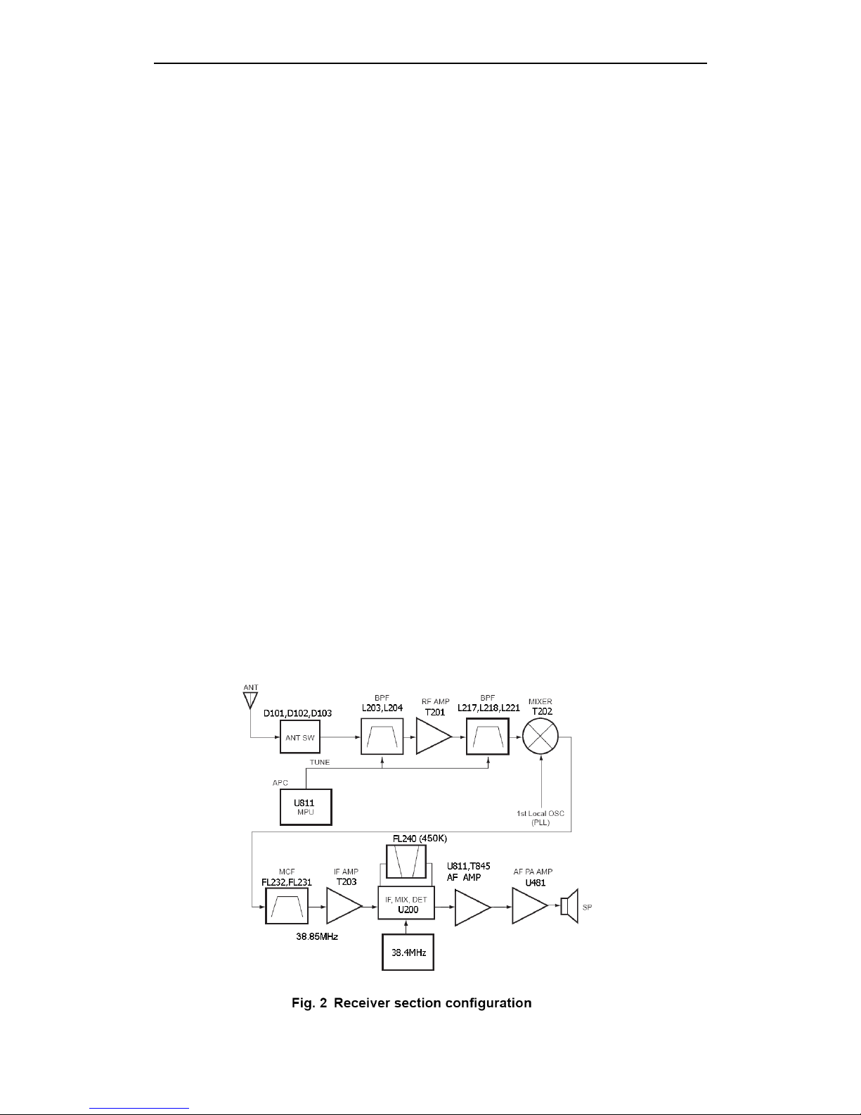
1. Frequency configuration
The receiver utilizes double conversion. The first IF is 38.85MHz and the second IF is
450kHz. The first local oscillator signal is supplied from the PLL circuit. The PLL circuit in
the transmitter generates the ecessary frequencies. Fig. 1 shows the frequencies.
2. Receiver
The freauency configuration of the receiver is shown in Fig.2.
1) Front - end RF amplifier
An incoming signal from the antenna is applied to an RF amplifier (T201) after passing
through a transmit/receive switch circuit (D101 ,D102,D103) and a 3-pole LC
filter(L203,L204).After the signal is amplified (T201), the signal is filtered by a band pass
filter (a 3-pole LC filter) (L217,L218,L221) to eliminate unwanted signals before it is
passed to the first mixer. The voltage of these diodes are controlled by to track the
MPU(U811) center frequency of the band pass filter. (See Fig. 2)

BLITZ MJ-398U
4
2) First Mixer
The signal from the RF amplifier is heterodyned with the first local oscillator signal from
the PLL frequency synthesizer circuit at the first mixer (T202) to create a 38.85MHz first
intermediate frequency (1st IF) signal. The first IF signal is then fed through crystal filters
(FL231,FL232) to further remove spurious signals.
3) IF amplifier
The first IF signal is amplified by T203, and then enters U200 (FM processing IC). The
signal is heterodyned again with a second local oscillator signal within U200 to create a
450kHz second IF signal. The second IF signal is then fed through a 450kHz ceramic filter
(FL240) to further eliminate unwanted signals before it is amplified and FM detected in
FL240.
4) AF amplifier
The recovered AF signal obtained from U200 goes to the microprocessor(U811). The
processed AF signal passes through an AF volume control and is amplified to a sufficient
level to drive a loud speaker by an AF power amplifier (U481).
5) Squelch
Part of the AF signal from the IC enters the FM IC again,and the noise component is
amplified and rectified by a filter and an amplifier to produce a DC voltage corresponding
to the noise level. The DC signal from the FM IC goes to the analog port of the
microprocessor (U811). U811 determines whether to output sounds from the speaker by
checking whether the input voltage is higher or lower than the preset value.To output
sounds from the speaker, U811 sends a high signal to the AF Power Iines and turns U481
on through T471,T472.
6) Receive signaling
QT/DQT
The output signal from FM IC (U200) enters the microprocessor(U811) .U811 determines
whether the QT or DQT matches the preset value, and controls the AF Power and the
speaker output sounds according to the squelch results
3. PLL frequency synthesizer
The PLL circuit generates the first local oscillator signal for reception and the RF signal for
transmission.
1) PLL
The frequency step of the PLL circuit is 5 and 6.25kHz and so on. A 16.8MHz reference
oscillator signal is divided at U301 by a fixed counter to produce the 5 or 6.25kHz
reference frequency. The voltage controlled oscillator (VCO) output signal is buffer
amplified by T373, then divided in U301 by a programmable counter . The divided signal is
compared in phase with the 5 or 6.25kHz reference signal in the phase comparator in
U301. The output signal from the phase comparator is filtrered through a low-pass filter
and passed to the VCO to control the oscillator frequency.
2) VCO
The operating frequency is generated by T331 in transmit mode and T357 in receive
mode. The oscillator frequency is controlled by applying the VCO control voltage, obtained
from the phase comparator, to the varactor diodes (D331 and D332 in transmit mode and
D350 and D351 in receive mode). The TC/RC pin is setlow in receive mode causing T192
off, and turn T291 on . The TC/RC pin is set hight in transmit mode causing T291 off,and
T192,T191 on.

BLITZ MJ-398U
5
3) UNLOCK DETECTOR
If a pulse signal appears at the LD pin of U301, an unlock condition occurs, and the DC
voltage obtained from D309, and C306 causes the voltage applied to the PLL-LD pin of
the microprocessor to go low. When the microprocessor detects this condition, the
transmitter is disabled, ignoring the push-totalk switch input signal. ( See Fig.3)
4. Transmitter
1)Microphone Amplifier
The signal from the microphone passes through U411.When encoding DTMF,it is turned
OFF for muting the microphone input signal by T414.The signal passes through the Audio
processor(U411) for the maximum deviation adjustment,and goes to the VCO modulation
input.
2)Drive and Final Amplifier
The signal from the T/R switch(D100) is amplified by the pre-drive(T101.T102) and drive
amplifier(T105) to 50mW.The output of the drive amplifier is amplified by the RF power
amplifier(T107) to 4.0W(1W when the power is low).the RF power amplifier consists of two
MOS FET stages.The output of the RF power amplifier consists of two MOS FET stages.
The output of the RF power amplifier is then passed through the harmonic filter (LPF) and
antenna switch (D101,D102)and applied to the antenna terminal.
5. Power supply
There are four 5V power supplies for the microprocessor: 5M,5C,5R,and 5T,5M for
microprocessor is always output while the power is on.5M for microprocessor is always
output while the power is on.5M is always output,but turns off when the power is turned off
to prevent malfunction of the microprocessor.
5C is a common 5V and is output when SAVE is not set to OFF.
5R is 5V for reception and output during reception.
5T is 5V for transmission and output during transmission.
6.Control Circuit
The control circuit consists of a microprocessor (U811) and its peripheral circuits.it
controls the TX-RX unit.U811 mainly performs the following:
(1) Switching between transmission and reception by the PTT signal input.
(2) Reading system,group,frequency,and program data from the memory circuit.
(3) Sending frequency program data to the PLL.
(4) Controlling squelch on/off by the DC voltage from the squelch circuit.
(5) Controlling the audio mute circuit by the decode data input.
(6) Transmitting tone and encode data.
BLITZ MJ-398U
6
1)Memory Circuit
Memory circuit consists of the CPU (U811) and an EEPROM(U821).An EEPROM has a
capacity of 32k bits that contains the transceiver control program for the CPU and data
such as Transceiver channels and operation features
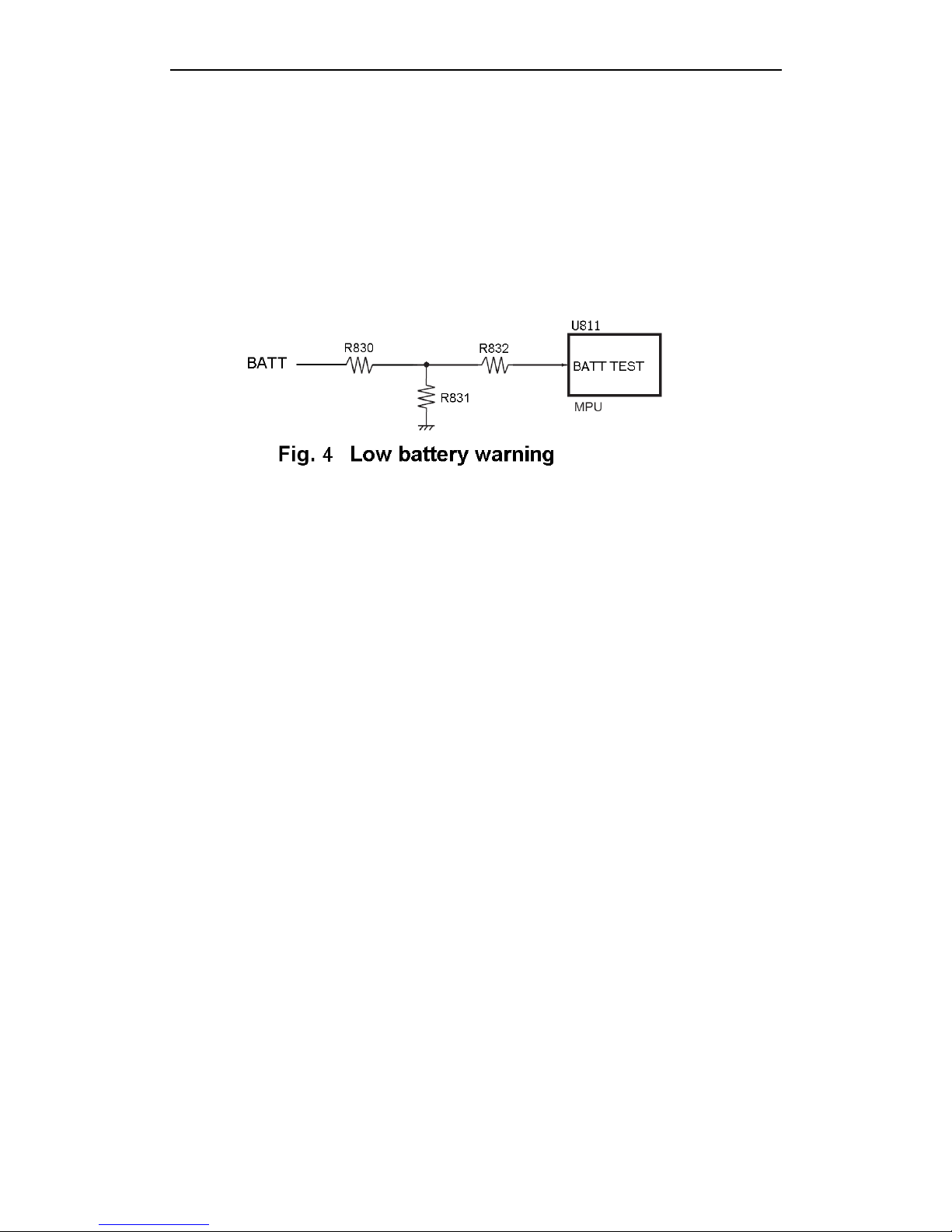
2)Low Battery Warning
The battery voltage is checked using by the microprocessor.
(1) The red LED blinks when the battery voltage falls below 6.2V.
(2) A Warning tone generates when the red LED blinking. ( See Fig.4)
 Loading...