

Page 1

M
i
M
M
7
7
V
V
I
I
Q
Q
Q
I
V
7
FCC S t a tement and Copyri ght
This equipment has been test ed and found to comply with the limits of a Class B
digit al device, pursuant to Part 15 of the FCC Rules. These lim its are designed t o
prov ide reasonable protection against harmful interference in a residential
installation. This equipment generates, uses and can radiate radio frequency
energy and, if not installed and used in accordance with the instructions, may
cause harmf ul interference to radio comm unications . There is no guarantee t hat
interferenc e will not occur in a part ic ular installat ion.
The v endor makes no representations or warranties with respect to the cont ents
here of an d spec ia lly dis c laims any implied warrant ies of m erc hantability or f itn ess
f or any purpose. Furt her the vendor reserv es the right to revis e t his publication
and t o m ake c hanges to the cont ents here of wit hout obligation to not ify any party
bef orehand.
Duplication of this publication, in part or in whole is not allowed without first
obt aining t he v endor’s approval in writing.
The c ontent of this us er’s is subject to be c hanged without notice and we will not
be res ponsible for any m ist akes f ound in this user’s manual. All the brand and
produc t names are trademarks of t heir respect ive companies.
Page 2

C
n
o
C
n
o
C
ENGLISH.............................................................................................3
M7VIQ Features (for V1.2)....................................................................... .....................................3
Package contents...........................................................................................................................4
Layout of M7VIQ.............................................................................................................................5
CPU Ins tallation......................................................................................... .....................................6
DDR DIMM Module s: DDR1-2............................................... .......................................................7
Jum pers, Head ers, Connectors & S lots.................................................................................. .8
s
t
n
e
t
s
t
n
e
t
s
t
n
e
t
n
o
ESPAÑOL..........................................................................................14
Características del M7VIQ..........................................................................................................1 4
Conten ido del Pa quete ........................................ .......................................................................1 4
Disposición del M7VIQ ........................................................... .....................................................1 5
Instalac ión del CPU............................................... .......................................................................1 6
Módulos DDR DIMM: DDR1-2....................................................................................................17
Conectores, Cab e zales, Puentes y R a nuras........................................................ .................1 8
FRANÇAIS.........................................................................................24
M7VIQ Particularités (pour V1.2) ...... ........................................................................................24
Dessin d’M7VIQ...................................................... .......................................................................25
WARPSPEEDER................................................................................26
Introduc tion ...................................................................................................................................26
System Requirement ...................................................................................................................27
Installation...................................................................................................................................... 27
Usage............................................................................................................ .............. .....................29
TROU BLE SHOOTING .......................................................................35
SOLUCIÓN DE PROBLEMAS.............................................................36
ii
Page 3

English
M7VIQ Features (for V1.2)
CPU
- Single AMD Socket-A for Athlon
processors.
- Running at 200/266 MHz Front Side Bus.
Chipset
- Nort h Bridge: VIA KM266 (VT8375).
- South Bridge: VT8235.
Main Me mo ry
- Support s up to 2 DDR dev ic es.
- Support s 200/266MHz (without ECC) DDR SDR AM devices.
- The largest memory capacity is 2GB.
Slots
- Three 32-bit PCI bus master s lots .
- One CNR slot.
- One AGP slot.
On Board IDE
- Supp orts four IDE dis k dri ves .
- Supports PIO Mode 4, Master Mode and Ultra DMA 33/66/100/133 Bus
Master Mode.
On Bo ard VGA
- Int egrated Savage4 2D/3D Graphics Controller and Video Accelerat or.
LAN Chipset
- VIA VT6103(Optional)
Audio
- AC97 2.1 int erfac e.
- PC99 complaint
- Support s 2 c hannels .
On Board Peripherals
- Support s 360K, 720K, 1.2MB, 1.44MB and 2. 88MB f loppy disk driv ers .
- Support s 2 s erial ports.
- Support s 1 m ult i-m ode parallel port . (SPP/EPP/ ECP m ode)
- Support s PS/2 m ous e and PS/2 keyboard.
- Support s 2 back U SB2.0 ports and 2 f ront U SB2.0 ports(Optional).
BIOS
TM
(ThunderbirdTM)/ At hlon
TM
XP / D uron
TM
3
Page 4

- AWARD legal Bios.
- Supports APM1.2.
- Supports ACPI.
- Supp orts USB Function.
Operating System
- Off ers the highest perform ance f or MS-DOS, Windows 2000, Windows Me,
Windows XP, SC O UNIX etc.
Dimensions
- Micro ATX Form Factor: 24.4cm X 24.4cm (W X L)
Pac kage con tents
- HDD Cable X 1
- FDD Cable X 1
- Fully Setup Driv er CD X 1
- Flas h Mem ory Writ er f or BI OS update X 1
- USB Cable X 2 (Optional)
- Rear I/ O Panel f or ATX C as e X 1 (Opt ional)
4
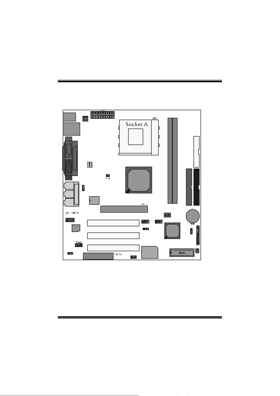
Page 5
Layou t of M7VIQ
V
V
JKBMS1
JCO M1
JV GA 1
JSPKR1
SP-OUT
JLIN1
LINE-IN
JMIC1
MIC-IN
JA UD GA ME
2910
1
Co d ec
1
JCODECSEL
JK BV1
1
1
JU SBV1
JUSB LAN1
JPRNT1
GA M E P o rt
1
JCFA N1
JU SB V3
1
1
1
LAN C HIP
JATXP WER1
T837 5
(KM 266)
PCI 1
2
1
JU SB2
1
PCI 2
PCI 3
Winbond
JWOL1
W8 36 97 HF
1
10
2910
9
1
JUSB3
JUSBV2
DDR1
JD IMM VOLT
8
127
T 82 35
1
JD J1 5
FDD 1
PRIM ARY IDE CON N.
IDE1 IDE2
FLOPPY DI SK CON N.
SEC O ND AR Y IDE CO NN .
DDR2
BAT1
2324
1
JCMOS1
JPANEL1
JSFAN1
1
12
5
Page 6
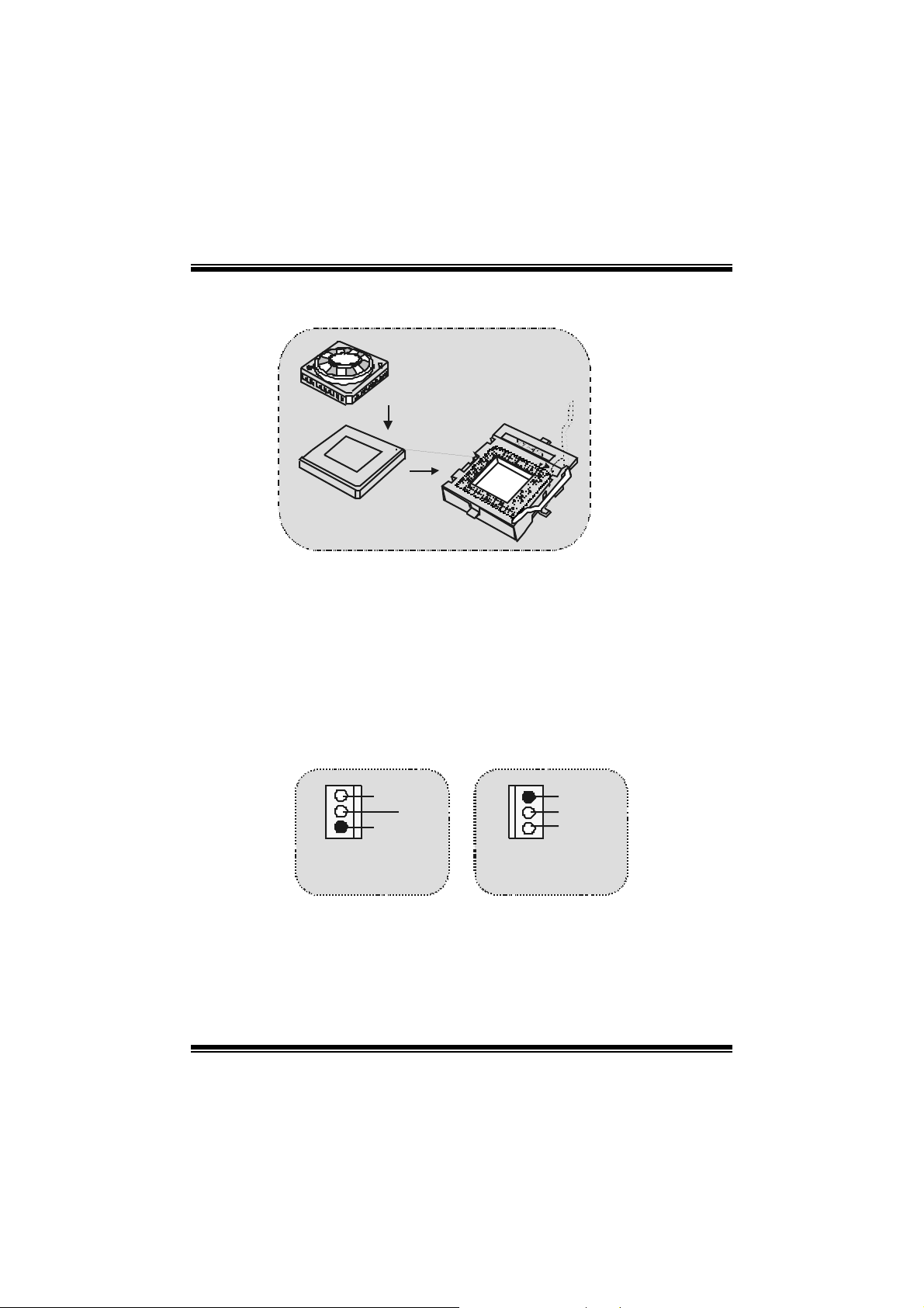
CPU Installation
C
P
U
1. Pull the lev er s ideways away f rom the socket then raise the lev er up to
90-degree angle.
2. Locat e Pin A in the socket and lock f or the white dot or c ut edge in t he CPU .
Match Pin A with the white dot/ c ut edge then insert the C PU.
3. Press the lever down. Then Put the f an on the CPU and buckle it and put the
fan’s power port into the JCFAN1, then to c omple te the instal lation.
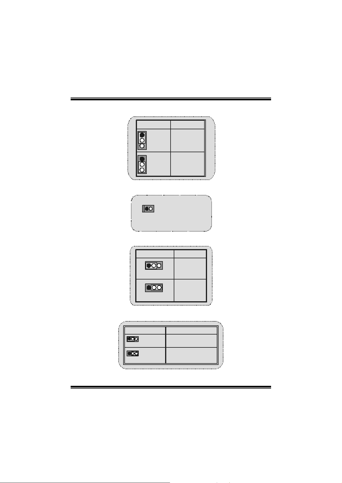
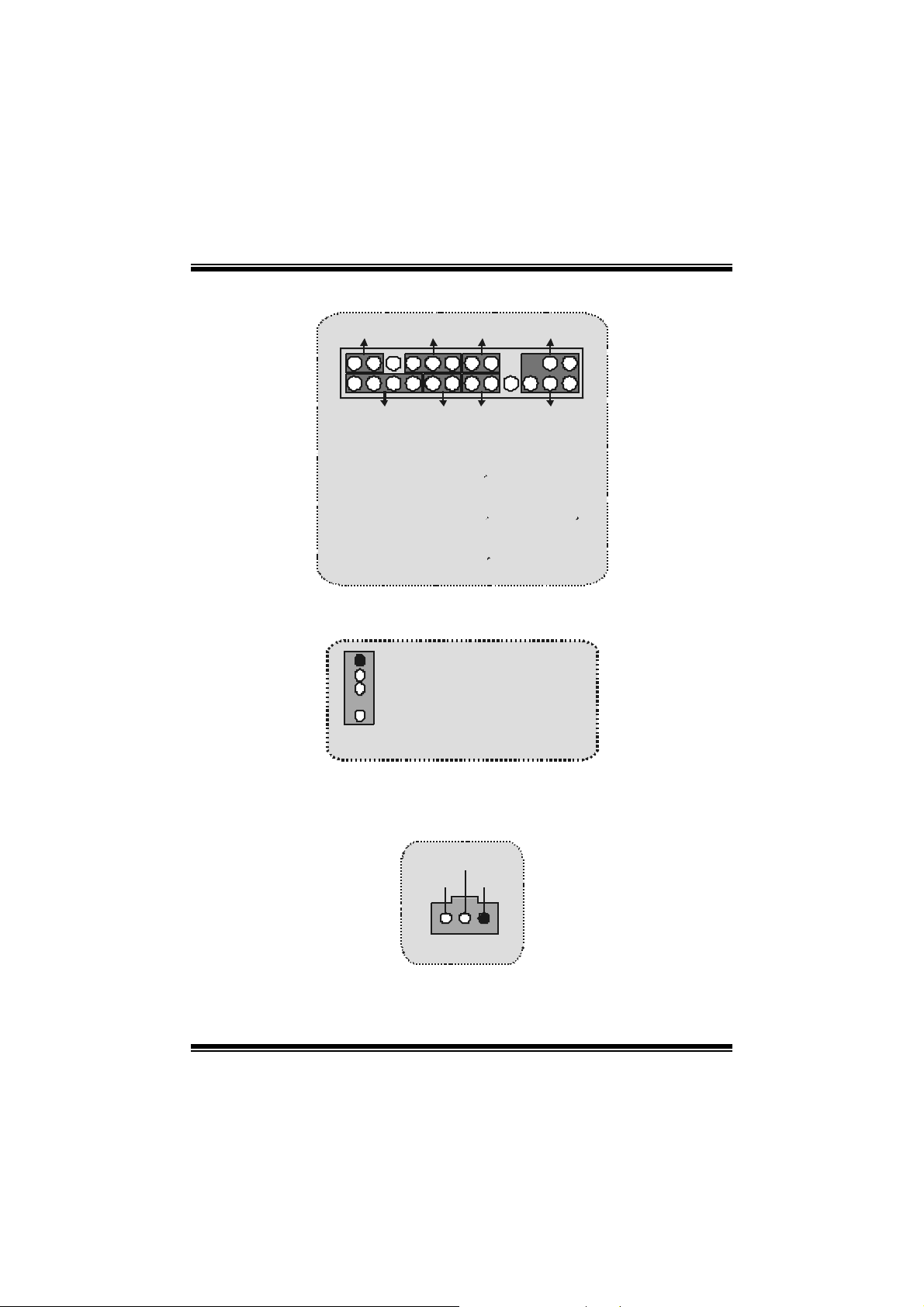
CPU/ System Fan Headers: JCFAN1/ JSFAN1
1
JSFAN1 JCFAN1
Ground
12V
Sense
1
Sense
12V
Ground
6
Page 7
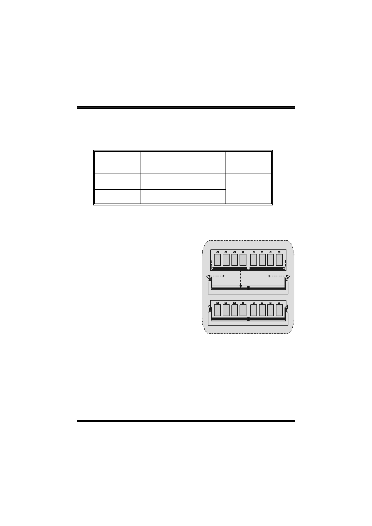
DD R DI M M Mo dules: D D R1- 2
DRAM Access Tim e: 2. 5V Unbuffered DDR 200/266 MHz Ty pe required.
DRAM Ty pe: 64MB/ 128MB/ 256MB/ 512MB/ 1GB D IMM Module (184 pin)
DIMM Socket
Location
DDR 1 64MB/128MB/256MB/ 512MB/ 1GB
DDR 2 64MB/128MB/256MB/ 512MB/ 1GB
* The list shown abov e for DRAM conf igurat ion is only for ref erence.
DDR M odule To ta l Memory
Size (MB)
*1
*1
Max is
2GB
How to install a DIMM Module
1. The DIMM socket has a “ Plas tic Safety
Tab”, and the DIMM memory module has
an “Asym metrical notch”, so the DIMM
memory module can only fit into the slot in
one direc t ion.
2. Push the tabs out. Insert the DIMM
memory modules into the socket at a
90-degree angle, then push down v ertically
so that it will fit into the place.
3. The Mounting Holes and plastic tabs
should fit ov er t he edge and hold t he DIMM
mem ory mo dules i n pl ac e.
7
Page 8

(
)
(
)
Jumpers, Headers, Connectors & Slots
Hard Disk Connectors: IDE1 / IDE2
The motherboard has a 32-bit Enhanced PCI IDE Controller that provides PIO
Mode 0~4, Bus Master, and Ultra D MA / 33/ 66/ 100/ 133 functionality. I t has two
HDD connec t ors ID E1 (primary) and IDE2 (s econdary ).
The ID E connect ors can connec t a master and a slave driv e, s o you can connect
up t o f our hard disk drives. The first hard drive should always be c onnected to
IDE1.
Floppy Disk Connector: FDD1
The motherboard provides a s tandard f loppy dis k c onnec tor t hat supports 360K,
720K, 1.2M, 1.44M and 2.88M floppy disk types. This connector supports the
prov ided f loppy driv e ribbon cables .
Commun ication Netw o rk Rise r Slot: CNR 1
The CNR specification is an open I ndust ry Standard Architecture, and it def ines a
hardware scalable riser c ard int erf ace, whic h supports m odem only.
Peripheral Component Interconnect Slots: PCI1-3
This m ot herboard is equipped with 3 standard PCI slots . PCI stands for Peripheral
Component Interc onnect, and it is a bus st andard f or expansion cards. This PCI
slot is designated as 32 bit s.
Accelerated Graphics Port Slot: AGP1
Unlike t he m ouse ports, key board port s and printer ports, this motherboard does
not hav e built in video facilit ies; and theref ore, requires a video card for one of t he
expansion slots. Your monitor will attach directly to that video card. Tis
motherboard supports video cards for PCI, but is also equipped with an
Accelerated Graphics Port (AGP). An AGP card will take advantage of AGP
technology f or improved video efficiency and performance, especially with 3D
graphics.
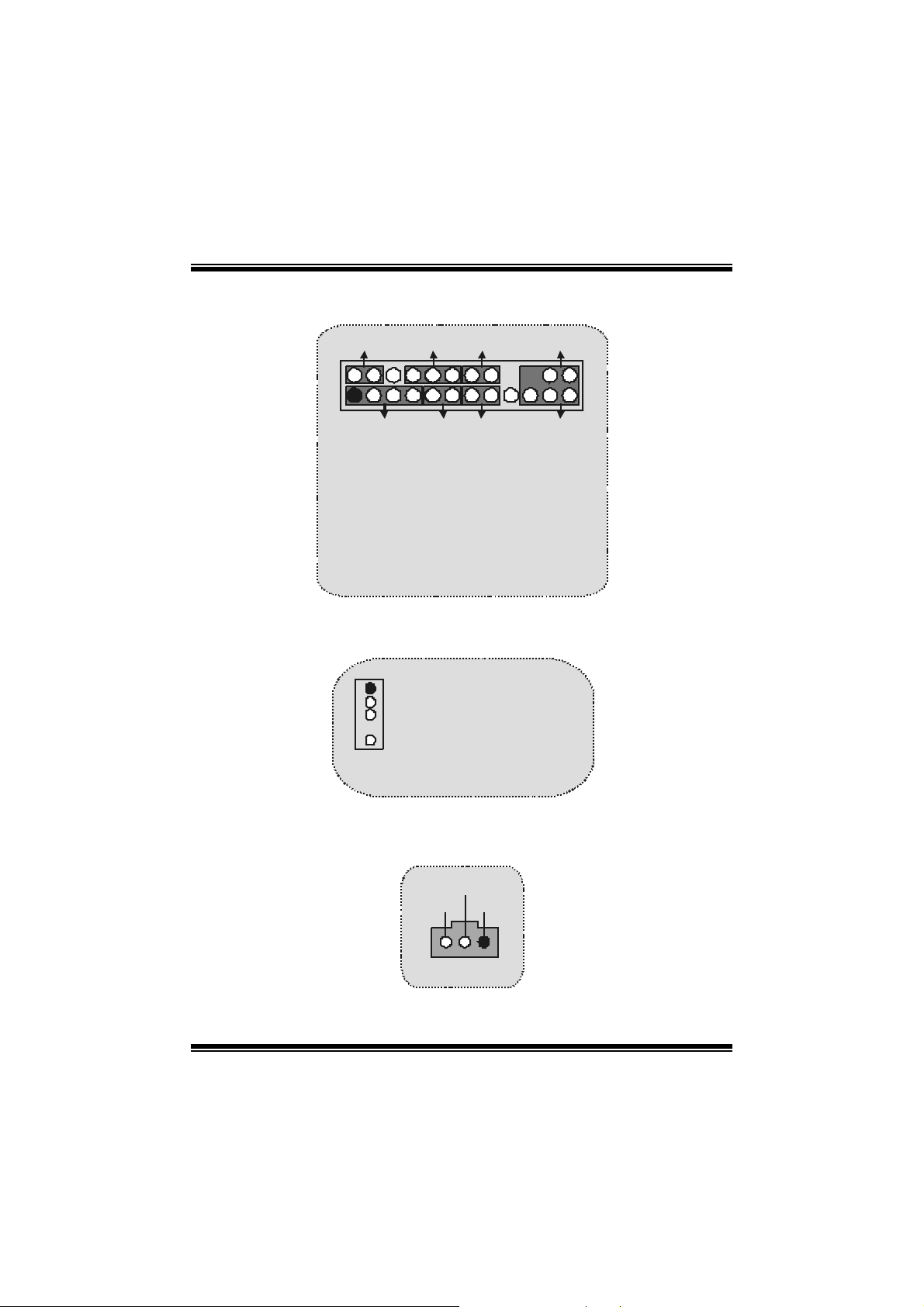
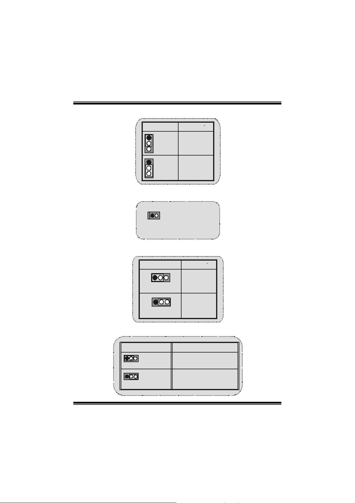
Power Connectors: JATXPWR1
JATXPWR1
JATXPWR1
ATX Main Power Conn.
ATX Main Power Conn.
8
Page 9
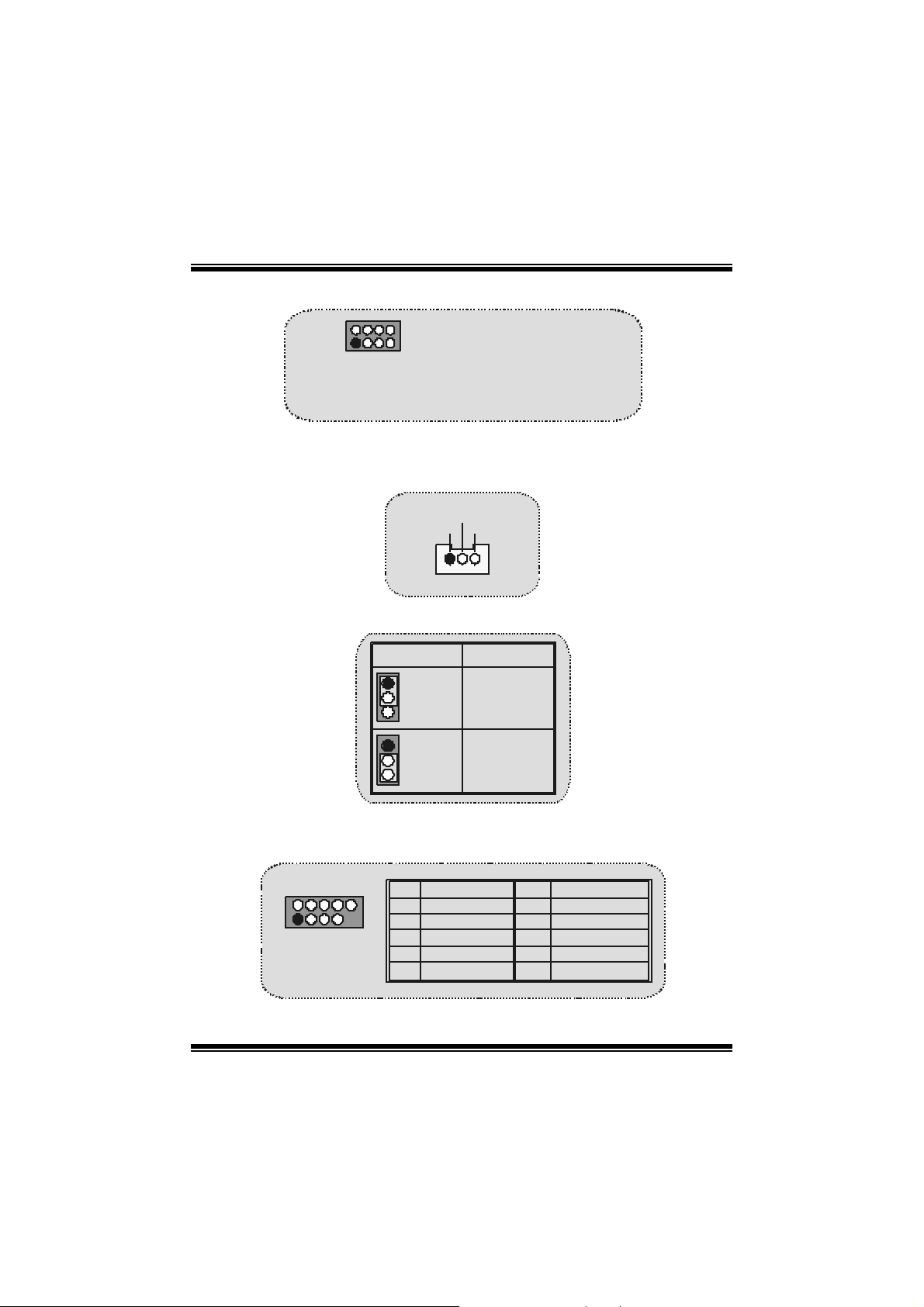
D IMM Power Selection Connector: JDIMMVOLT
z It strongly recomm ended t o set DDR DIMM v oltage in default sett ing 2. 5V,
and it for over v oltage fu nction.
2
1
JDIMMVOLT
(Default ==> 2.5V)
Pin 1-2 on ==> 2.5V
Pin 3-4 on ==> 2.6V
Pin 5-6 on ==> 2.7V
Pin 7-8 on ==> 2.8V
Wake On LA N Header: WO L1
Ground
5V_SB Wake up
1
WOL1
Clear CMOS Jumper:JCMOS
JCMOS1
1
Pin 1-2 on
1
Pin 2-3 on
Assignment
Nor m al
Operation
(default)
Clear CMOS
Data
Front USB Header: JUSB2/ JUSB3
2
1
JUSB 1 /2
Pin Assignment Pin Assignment
12
+5V +5 V
43
Da ta (-)D at a (-)
56
D ata (+ ) Data (+)
Ground Ground
910
Key NA
87
9
Page 10
5V/ 5VSB Selection for USB: JUSBV1/2/3
JUSBV1/2/3
1
Pin 1-2 o n
1
Pin 2-3 o n
Assignment
5V
5V_SB
CPU Frequency Selection: JCLK1
1
JCLK1
On ==> 100MH z
Of f ==> 13 3 M H z
5V/ 5VSB Selection for Keyboard: JKBV1
JKBV1
1
Pin 1-2 on
1
Pin 2-3 on
Assignment
5V
5V_SB
C NR Codec Primary/ Secondary Selection: JCODECSEL
J_CODECSEL
Pin 1-2 On-board Primary
Codec (Default).
1
Pin 2-3 CNR P rimary Codec.
1
Assignment
10
Page 11
Front Panel Connector: JPANEL1
SLP
2
1
SP K == > Speake r Conn.
HLED ==> Hard Driver LED
RST ==> Reset Button
IR == > Infrare d Conn.
SLP ==> Sleep Button
P WR_ LED ==> Power LED
ON/ OFF ==> Power-on Button
SPK
PWR_LED
HLED
RST
IRON/OFF
IR
Audio DJ: JDJ1
JDJ1
1
Pin1 ==> SMBDT
Pin2 ==> SMBCK
P in3 ==> -INTR_B
5
Pin4 ==> NC
Pin5 ==> PWRGD
Digital Audio C onnector: JSPDIF1 (Opti onal)
SPDIF_ OUT
GND VCC5
1
JSPDIF 1
24
23
11
Page 12
(
)
(
)
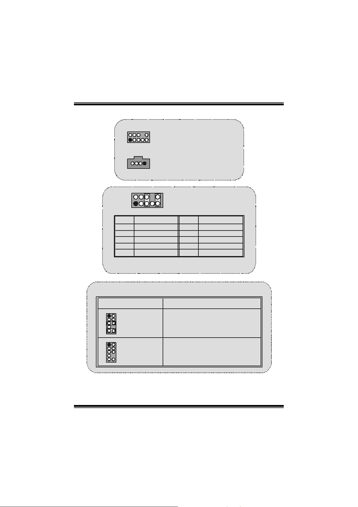
Audio Subsystem: JF_AUDIO/JCDIN1
2
1
1
2
2
1
Pin
1
3
5
7
9
Assignment
Mi c I n
Mi c Pow e r
RT L in e O u t
Reserved
LFT Lin e Out
Pin 5 and 9 are routed to Front Panel Audio Out.
Pin 6 an d 10 are r o uted fro m Front P a nel Aud i o Ou t .
JF_AUDIO1
F ront Audi o Header
JCDIN1
CD-ROM Au d io-In Hea d er
10
9
JAUDIO1
Pin
2
4
6
8
10
Assignment
Ground
Audio Power
RT L i n e Ou t
NC
L FT Line Out
Front Panel Audio Conne ctor/ Jumper Block
Jumper Setting Configuration
12
4
3
5
7
910
12
3
5
7
910
Pin 5 and 6
6
Pin 9 and 10
4
6
No jumper s
installed
Audio line out sign als are routed
to the back panel audio line out connector.
Audio line out and mic in signals are
ava ilable for front panel audio connectors.
12
Page 13
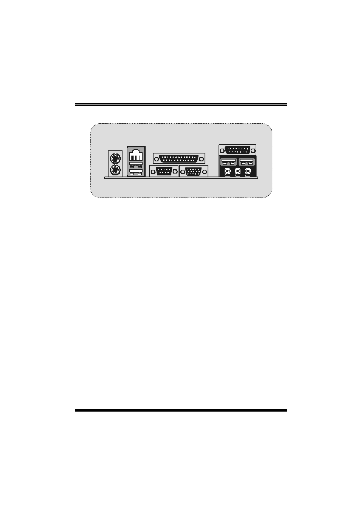
B ack Pa nel Connectors
(op
)
JKBMS1
PS/ 2
Mous e
PS/2
Keyboard
RJ45USB1
LAN(Optional)
USB
COM1
COM1
JCOM1
JPRNT1
Parallel
VGA1
JVGA1
JGAME1_USB1
Ga me Po r t /
USB Ports
Speake r
Line In Mic
Out
t ional
In
13
Page 14

Español
Características del M7VIQ
Usa C hipset Via KM266/ VT8235, W83697H F, LAN Chip (opcional).
Contiene fac ilidades I/O integrados en la placa madre en el que incluy e un puerto en
serie, un puerto paralelo, un puerto de ratón PS/ 2, un puerto de teclado PS/ 2, puert o
de audio, puert os USB, un puert o LAN (opcional), un puerto de juego, y un puerto
para el m onitor.
Soporta single AMD Sock et A para proces adores Athlon™ (Thunderbird™) / Athlon
XP™ / Du r o n ™ c orriendo a 200/ 266 MHz Front Side Bus (FSB).
Soporta U ltra 133/100/ 66/33, modos PIO, disc os duros IDE, modo LBA.
Soporta 2 dispos itivos DDR 200/266 MHz (s in ECC).
Soporta una ranura CNR (solamente de Tipo B), tres ranuras PCI Bus de 32-bit, y
una ranura A GP.
Conform a con las es pecif icac iones del fact or de forma de tamaño PC Micro-ATX.
Soporta sistemas operativos populares tales como Windows NT, Windows 2000,
Windows ME, Windows XP, LINUX y SCO UNIX.
Compatible con Via
High S/N ratio reune los requisitos del PC 99.
4CH D AC, aplic ables para chips ets de princ ipales plac as madres.
Entrada de Línea phonejack com partido con el rear out.
®
A C ’9 7 2 .2.
Contenido del Paquete
C able H D D X 1 , C able F D D X 1, C onfi g urac i ón C om pleta de l Driv er CD X 1
Flash Mem ory Writer para actualización del BIOS X 1
Cable USB X 2 (Opc ional)
14
Page 15
V
Panel Trasero I/O para Caja ATX X 1 (Opcional)
D is po s i ción de l M 7VI Q
JKBMS1
JCOM1
JVGA1
JS PK R1
Salid a del
Altavoz
JLIN1
Ent rada
de Li nea
JMIC1
En t rad a
de MI C
JAUD GAME
10
129
Codec
J C ODE CSEL
1
JKBV1
1
1
JUSBV1
JUSBLAN1
JPRN T1
Puerto de J uego
J CF AN1
JUS B V3
1
1
1
LAN CHIP
JATXPWER1
KM 266
PCI1
2910
1
JUS B 2
1
PCI2
PCI3
JW OL1
W 836 97 HF
1
JUSBV2
Winbond
JDI MMVOLT
2910
1
JU SB 3
127
DDR1
8
T 8235
DDR2
PRIMARY IDE CONN.
IDE1IDE2
BAT1
JCMOS 1
J PANE L 1
JSFAN1
FDD1
1
1
FLOPPY DI SK CONN.
SEC ONDA RY IDE CONN .
23
24
12
15
Page 16
Instalac ión del CPU
C
P
U
palanca del lado del zócalo, luego levante la palanc a has ta un ángulo de 90
grados.
2. Sitúe el cont acto A del zócalo y busque el punto blanco o c orte el borde en la
CPU . Em pareje el c ontacto A con el punto blanco/ corte del borde, luego
inse rte la C PU.
3. Presione la palanc a para abajo. Ponga el v entilador en la CPU y abróchelo.
Luego ponga el puerto de corriente del vent ilador en el JC F AN1. Y ya habrá
com pletado s u instalación.
CPU/ Cabezales del Sistema de Ventil ación: JCFAN1/ JSFAN1
1
Sense
12V
Tierra
1
Tierra
12V
Sense
JCFAN1
JSFAN1
1. Tire de la
16
Page 17
Módulos DDR DIMM: DDR1-2
DRAM Tiempor de Acceso: 2.5V U nbuff ered DDR 200/266 MH z Tipo requerido.
DRAM Tipo: 64MB/ 128MB/ 256MB/ 512MB/ 1GB Módulo DIMM (184 pin)
Loca lización
del Módulo
DIMM
DDR 1 64MB/128MB/256MB/ 512MB/ 1GB
DDR 2 64MB/128MB/256MB/ 512MB/ 1GB
* La list a de arriba para la configuración DRAM es solamente para ref erencia.
M ódul o DDR
*1
*1
T otal del
Tamaño de
Me m o r ia (MB)
Máximo de
2GB
Cómo instalar un Módulo DIMM
1. El zócalo DIMM tiene una lengüeta
plástica de seguridad y el módulo de
memoria DIMM tiene una muesca
asimétrica, así el módulo de memoria
DI MM puede caber s olamente en la ranura
de una s óla dirección.
2. Tire la lengüeta hacia afuera. Inserte
los módulos de memoria DIMM en el
zócalo a los 90 grados, luego empuje hacia
abajo verticalmente de modo que encaje
en el lugar.
3. Los agujeros de montaje y las lengüetas
plásticas deben caber por s obre el borde y
sostenga los módulos de memoria DIMM
en el lugar.
17
Page 18

(
)
Conectores, Cabezales, Puentes y Ranuras
Conectores del Disco Duro: IDE1/ IDE2
La plac a madre tiene un controlador de 32-bit PCI IDE que proporc iona Modo PIO
0~4, Bus Master, y funcionalidad Ult ra DMA / 33/ 66/ 100. Tiene dos conect ores
HD D IDE1 (pr i mario ) y IDE2 (se cundario).
El conector IDE puede conectar a un master y un drive esclavo, así puede
conectar hasta cuatro discos rígidos. El primer disc o duro debe es tar siem pre
conectado al IDE1.
C on ector para el Disquete: FDD1
La plac a madre proporciona un conect or estándar del dis quete (FDC) que soport a
360K, 720K, 1.2M, 1.44M y 2.88M tipos de disquet e. Éste conector utiliza los
cables de cint a proporcionados por el disquete.
Banda de Suspensi ón de Comunicación y Red: CN R1
La especificación CNR es una abierta Industria de Arquitectura Estándar, que
def ine una tarjeta de interface escalable del hardware en el que soporta
solamente mode m.
Ranura de Intercone x ión del Componente Periférico: PCI1-3
Ésta plac a madre est á equipada con 3 ranuras est ándar PCI . PCI es la sigla para
Interconexión del Componente Perif érico, y es un bus estándar para tarjetas de
expansión en el que s uplant a a la ant igua bus est ándar ISA, en su mayoría de las
part es . Ésta ranura PCI está diseñado con 32 bit s.
Ranu ra del Puerto Acelerado para Gráficos: AGP1
Su m onitor s e fijará directamente a la tarjet a de video. Ésta placa m adre soport a
tarjetas de v ideo para ranuras PCI, y también está equipado con un Puerto
Acelerado para Gráficos (AGP/ solamente soporta 1.5V y 4X tarjeta AGP). Ésta
tarjeta AGP t omará vent aja de la tecnología del AGP para el mejoramiento de la
eficiencia y fun cionamien to del video , e special m ente con gráfi cos 3D.
Conectores de Corriente: JATXPWR1
JATXPWR 1
(ATX Main Po wer Co nn.)
ATX Cone ctor de Corrien te Principal.
JATXPWR 1
18
Page 19
Conector de Selección de la Corrie nte DIMM: JDIMMVOLT
z Ést a fuertem ente recomendado f ijar el v oltaje del DDR DIMM en su v oltaje
predeterm inado 2. 5V, and it f or over volt age f unct ion.
JDIMMVOLT
JDIMMVOLT
(P re de ter mina do == > 2.5V )
(P re de ter mina do == > 2.5V )
1
1
2
2
Pin 1-2 encend ido ==> 2.6V
Pin 1-2 encend ido ==> 2.5V
Pin 3-4 encend ido ==> 2.7V
Pin 3-4 encend ido ==> 2.6V
Pin 5-6 encend ido ==> 2.8V
Pin 5-6 encend ido ==> 2.7V
Pin 7-8 encend ido ==> 2.9V
Pin 7-8 encend ido ==> 2.8V
Cabezal Wake On LAN: WO L1
Tierra
5V_SB Wake up
1
WOL1
Puente de BorrarCMOS: JCMOS1
JCMOS1
1
Contacto
1-2 on
1
Contacto
2-3 on
Asignacion
Operacion
Normal
(default)
Borrar Dat os
CMOS
Cabez al Frontal USB: JUSB2/ JUSB 3
Contactos Asignacion Contactos Asignacion
2
1
12
56
+5V +5V
Data (+) Data (+)
Tierra Ground
910
Key NA
JUSB2/ 3
43
87
Data (-)Data (-)
19
Page 20
g
5V/ 5VSB Selección pa ra USB: JUSBV1/2/3
JUSBV1/ 2/ 3
1
Contactos
1-2 on
1
Contactos
2-3 on
Asignacion
5V
5V_SB
S elección de Frecu encia del CPU: JCLK 1
1
JCLK1
On ==> 100MHz
Of f ==> 13 3 M H z
5V/ 5VSB Selecci ón para Teclado: JKBV1
JKBV1
1
Contactos 1-2 on
1
Contactos 2-3 on
Asignacion
5V
5V_SB
CNR Codec de Selección Primario/ Secundario: JCODECSEL
J_CODECSEL
Contacto
1-2
1
Contacto
1
2-3
Assignment
Code c Prima rio
inte
rado en l a placa madre.
CNR Codec P rimari o.
20
Page 21
j
Conector del Panel Frontal: JPANEL1
SLP
224
123
SPK ==> Conector de Altavoz
HLED == > LED del Di sco Duro
RST ==> Boton de Reinicio
IR ==> Conector Infraro
SLP == > Bo t on d e Su sp en s i o n
P WR_ LED ==> Corriente LED
ON/ OFF ==> Bot on de Ence ndid o
SPK
PWR_LED
HLED
RST
IRON/OFF
IR
o
Audio DJ: JDJ1
JDJ1
Contacto1 ==> SMBDT
1
Contacto2 ==> SMBCK
Contacto3 ==> -INTR_B
Contacto4 ==> NC
5
Contacto5 ==> PW RGD
Conector Digital de Audio: JSPDIF1 (O ptional)
SPDIF_ OUT
GND VCC5
1
JSPDIF 1
21
Page 22

_
(
)
(
Subs iste ma de Audio: JF_AUDIO/JCDIN 1
Contactos
Contactos 5 y 9 so n encaminados a la Sal ida de Audi o del Pane l
Frontal.
Conta ctos 6 y 10 son en caminados desde la Salida de Audio de l
Pane l Fronta l.
2
1
2
2
1
Asignacion
1
3
5
7
9
Entrada del MIC
Corr iente del MIC
RT Salida de Linea
Reservado
LFT Sal ida de Line a
Cab ezal F ron tal de Au dio
Cab ezal de Entrada de
1
Au dio CD-ROM)
10
9
AUDIO1
JF
JCDIN1
JAUDIO1
Contact os
2
4
6
8
10
Corriente de A udio
RT Salida de Linea
LFT Salida de Linea
Asignacion
Tierra
Key
Conector del Panel Frontal de Audio/ Jumper Block
Jumper Setting Configuracion
~
12
4
3
5
7
910
12
3
5
7
910
Contacto 5 & 6
6
Contacto 9 & 10
4
No jumper s
6
installed
La se nal de salida de linea del Au dio
encamina al conector de la salida de linea
del Au dio ubicado en el panel trasero .
~
La se nal de salida de linea del Au dio y la
~
senal del en trada del mic esta n dispon ibles
desde el conector de Audio del
panel frontal.
22
Page 23

Conectores del Panel Trasero
(op
)
JKBMS1
Raton
PS/2
Te clad o
PS/2
RJ45U SB1
LAN(Opcional)
USB
COM1
COM1
JCOM1
JPRNT1
Paralelo
VGA1
JVGA1
JGAME1_USB1
Pue r t o d e J u ego/
Puertos USB
Sa lida de l
Entrada
Altavoz
de L inea
cional
E n trad a de
Mic
23
Page 24

Français
M7VIQ Particularités (pour V1.2)
CPU :
- Douille-A AMD Simple pour AthlonTM (ThunderbirdTM) / AthlonTM
XP/ DuronTM proc es s eurs.
- Dirigeant à Autobus de Côté de F ront de MHz 200/266.
Chi p set :
- Pont du Nord : VIA KM266 (VT8375).
- Pont du Sud : VT8235.
Mémoire Principale :
- Soutient dis positif s jusqu'à 2 D DR .
- Soutient dispos itif s de DD R SDRAM (sans CEE).
- La plus grande capacité de mémoire(s ouvenir) est 2GB.
Fentes :
- Trois f ent es de m aît re d'autobus PCI 32 bits.
- Une fen te CNR.
- Une fente AGP.
À bord IDE :
- Soutient quat re lec t eurs de dis ques IDE.
- Soutient PIO Mode 4, le Mode de Maître et DMA Ultra 33/66/100/133 le
Mode de Maître d'Aut obus.
À bord V GA :
- Int égré Savage4 Cont rôleur Graphique 2D/ 3D et Acc élérateur Vidéo.
Ch ipset LAN :
- VIA VT6103 (Fac ult atif).
Audio :
- AC97 2.1 int erfac e.
- PC99 la plainte - Soutient 2 canaux.
À bord Périphériques :
- Soutient 360Ko, 720Ko, 1.2MB, 1.44MB et 2.88MB des conducteurs de
disquette.
- Soutient 2 ports périodiques.
- Soutient 1 mult i-m ode port parallèle. (SPP/ EPP/ECP m ode)
- Soutient le s ouris PS/2 et le clavier PS/2.
- Soutient 2 ports en arrière USB2.0 des et 2 ports en avant USB2.0 des
(Facultatifs).
24
Page 25

V
(
)
V
BIOS :
- ACCORD ENT le BIOS légal.
- Soutient APM1.2.
- Soutient ACPI.
- Soutient la Fonction d'USB.
Système de Fonctionnement :
- Off re l'ex écut ion(perf ormance) la plus haut e pour MS-DOS, Windows 2000,
des Fenêt res Moi, Windows XP, SC O UNI X etc.
D im e nsi ons :
- Micro F acteur de Forme d'ATX : 24.4c m X 24.4cm (W X L)
Dessin d’M7VIQ
JKBMS1
JKBV1
1
1
JUSB V1
J USB LAN1
JCOM1
JP RNT1
JATX PW ER 1
1
JDJ 1 5
FDD1
JCFAN1
1
JVGA1
JSPKR1
SP-OUT
JL I N1
LINE-IN
JMIC1
MI C -IN
JAUD GAME
129
1
JCODEC SEL
10
Codec
JUSB V3
1
LA N CH I P
GAME Port
1
1
T8375
KM 266
PCI1
2910
1
JUSB 2
1
PCI2
PCI3
JWOL 1
1
25
JUSB V2
Wi nbon d
W8369 7HF
2910
1
JUS B3
DDR 1
JD IM MVOLT
8
127
T 8235
DDR2
PR IM AR Y ID E CONN .
IDE1 IDE 2
BAT1
JCMOS1
JPANEL1
JS FA N1
FLOPPY DIS K CONN.
SEC ONDARY IDE CONN.
2324
1
12
1
Page 26

WarpSpeeder
Introduction
[ W arpSpeeder™ ], a new powerf ul control ut ility, f eatures three user-friendly functions
including Overclock Manager, Overvolt age Manager, and H ardware Monitor.
The f ollowing three sec tions det ail the installation of Fas tTrak 376 drivers on a sy st em
that has W indows 98/Me already inst alled. If you’re ins talling the F astTrak 376 drivers on
a syst em during a Windows 98/ Me installation, s ee “Installing Driv ers D uring Windows
98/Me Inst allat ion” on page 10. W ith t he Overc lock Manager, users can eas ily adjust t he
frequency they prefer or they c an get the best C PU perf ormanc e with just one click. The
Overvoltage Manager, on the other hand, helps to power up CPU core voltage and
Memory voltage. The cool Hardware Monitor smart ly indic ates t he t emperat ures, volt age
and CPU fan s peed as well as the chips et inform ation. Als o, in t he About panel, y ou c an
get detail descriptions about BIOS model and chips ets. In addition, the f requency st atus
of C PU, mem ory, AGP and PCI along with the C PU s peed are sy nchronic ally shown on
our main panel.
Moreover, to protect users' computer systems if the setting is not appropriate when
testing and results in system f ail or hang, [ WarpSpeeder™ ] technology assures the
sy stem st ability by automat ically reboot ing the c omputer and then restart t o a s peed that
is eit her t he original sys t em s peed or a s uit able one.
26
Page 27

System Requirement
OS Support: Windows 98 SE, Windows Me, Windows 2000, Windows XP
DirectX: D irect X 8.1 or abov e. (The Windows XP operating system in cludes D irec t X 8. 1.
If you use W indows XP, y ou do not need to inst all Direct X 8.1. )
Installation
1. Exec ute the s etup execution f ile, and then the f ollowing dialog will pop up.
Please clic k “Next ” button and follow the default procedure to inst all.
2. When you see the f ollowing dialog in setup procedure, it means setup is
com pleted. If the “Launch the W arpSpeeder Tray Ut ility” checkbox is checked,
the Tray Ic on utility and [ WarpSpeeder™ ] utility will be automatically and
imm ediately launched aft er you click “Finish” but t on.
27
Page 28

28
Page 29

Usage
The fo llowi ng fi gu r es ar e just only for r e f er enc e , t h e s cre en pr in ted in this u s er ma nual w ill
change according to your mot h erboard on hand.
[ WarpSpeeder™ ] includes 1 tray icon and 5 panels:
1. Tray Icon:
Whenev er t he Tray Icon utility is launched, it will display a litt le tray icon on the right s ide
of W indows Taskbar.
This ut ility is res pons ible f or c o nve niently invoking [ WarpSpeed er™ ] Utility. Yo u can use
the mouse by c licking t he lef t button in order to invok e [ WarpSpeeder™ ] direct ly from
the little tray icon or you can right-click the litt le tray icon t o pop up a popup menu as
following f igure. The “Launch Utility” item in the popup menu has t he same f unct ion as
mo us e left -click on tray icon and “E xit ” ite m will close Tray Icon utility if select ed.
2. Main Panel
If you click the tra y icon, [ WarpSpeeder™ ] utility will be in vo ke d. Please re fer
do the following figure; the u tilit y’s fi rst window you will s ee is Main Panel.
Main Pan el contains features as follows:
a. Display t he CPU Speed, CPU ex ternal clock, Memory cloc k, AGP c lock, and PC I
29
Page 30

cloc k inf ormat ion.
b. Contains About, Voltage, Overclock, and Hardware Monitor Buttons for invoking
respective panels.
c. With a user-friendly Status Animation, it can represent 3 overclock percentage
stages:
Man walking => overcloc k perc entage from 100% ~ 110 %
Pant her running => overc lock percentage from 110% ~ 120%
Car racing => ov erclock percent age from 120% ~ abov e
3. Voltage Panel
Click t he Voltage butt on in Main Panel, the button will be highlight ed and t he Voltage
Panel will slide out to up as the f ollowing f igure.
In this panel, you can decide to increas e CPU core voltage and Mem ory volt age or not.
The def ault setting is “No”. If y ou want to get t he best performance of ov erc locking, we
r ec o m m end y o u c lic k t h e opt i on “Y es”.
30
Page 31

4. Overclock Panel
Click t he Overclock butt on in Main Panel, the butt on will be highlighted and the Overclock
Panel will slide out to left as the f ollowing figure.
Overclock Panel contains the thes e features:
a. “–3MHz button”, “-1MHz button”, “+1MHz button”, and “+3MHz button”: provide
use r the ability to do real-time ov erc lock adjustm ent.
Warning: Manually overclock i s potentially dangerous, especiall y when the
overclocking percentage i s over 110 %. We strongl y recommend you verify
every speed you overclock by cli ck the Verify button. Or, you can just click
31
Page 32

Auto overcl ock button and let [ WarpSpeeder™ ] automatically gets the best
result for you.
b. “R ecovery Dialog button”: Pop up the following dialog. Let user select a rest oring
way if sy s t em need t o do a f ail-safe reboot.
c. “Auto-ov ercloc k butt on”: U s er can click t his button and [ WarpSpeeder™ ] will s et
the best and stable performance and f requency automatically. [ WarpSpeeder™ ]
utility will execute a series of testing until system fail. Then system will do fail-safe
reboot by using Watchdog function. After reboot, the [ WarpSpeeder™ ] utility will
rest ore to t he hardware def ault s ett ing or load t he verified best and st able f requency
according to the Recovery Dialog’ s setting.
d. “Verify button”: User can click this button and [ WarpSpeeder™ ] will proceed a
testing for current fr equenc y. I f the testing is ok, then the c urrent frequency will be
sav ed into system registry. If the testing f ail, syst em will do a fail-s afe rebooting.
After reboot, the [ WarpSpeeder™ ] ut ility will restore to the hardware default
setting or load the verif ied best and stable frequency acc ording to the Rec overy
Dialog’ s setting.
Note: Because th e testing p rograms, in voked in A u to-overcl ock and Verify,
i n clude Di re ctDraw , Direct3D an d DirectShow test s, the Di rectX 8.1 or newe r
runtime library i s required. And pl ease make sure your displ ay card’s color
depth is High color (16 bit) or True color( 24/32 bit ) that is required for
Direct3D rendering.
32
Page 33

5. H ardware Monit or Panel
Click t he Hardware Monitor butt on in Main Panel, the butt on will be highlight ed and the
Hardware Monitor panel will slide out to lef t as the following figure.
In t his panel, you c an get the real-t ime stat us inform ation of y our system. The inf ormation
will be ref res hed ev ery 1 s econd.
6. About Panel
Click the About butt on in Main Panel, the button will be highlighted and the About Panel
will slide out t o up as t he following f igure.
In t his panel, you can get model name and detail inf ormation in hints of all the chips et t hat
are related to overclocking. You can also get the mainboard’s BIOS model and the
Version number of [ WarpSpeeder™ ] utility.
33
Page 34

Note: Because the overclock, overvoltage, and hardware monitor features
are controlled by several separate chipset, [ WarpSpeeder™ ] divi de these
features to separate panels. If one chipset is not on board, the correlative
b u tto n i n Main pa n el wi ll b e d i sa bl ed, b u t wil l n ot int er fe re oth e r panel s’
functions. This property can make [ WarpSpeeder™ ] utility more robust.
34
Page 35

Trouble Shoo ting
e
e
k
y plugg
g up
y
pp
p
pp
d
prog
e
r
PROBABLE SOLUTION
No power to the sys tem at all Power light don’t
illuminate, fan inside power supply does not turn
on. Indicator light on keyboard does not turn on
PROBABLE SOLUTION
System inoperative. Keyboard lights are on,
power indicator lights are lit, hard drive is
spi n ni ng.
System does not boot from hard dis k drive, can
be booted from CD-ROM drive.
System only boots from CD-ROM. Hard disk can
be read and a
booting from hard disk is impossible.
PROBABLE SOLUTION
PROBABLE SOLUTION
lications can be used but
* Make sure power cable is securely plugged i n
* Replac e c abl e
* Contact techni c al s upport
* Using even pressure on both ends of th
DIMM, press down firmly until the modul
snaps into p l ace.
* Check cable running from disk to dis
controller board. Make sure both ends are
sec urel
the standard CMOS setup.
* Backin
important. All hard disks are capable o
breaking down at any time.
* Back u
the hard drive. Re-install a
data using backup disks.
ed in; check the drive type in
the hard drive is extremel
data and applications files. Reforma
lications an
PROBABLE SOLUTION
Screen message says “Invalid Confi gurati on” or
“CMOS Fail ure.”
* Review system’s equipment . Make sure
c or r ect infor m a t io n is in s et u p .
PROBABLE SOLUTION
Cannot boot system after ins talling second hard
drive.
* Set master/slave jum p e rs correctly.
* Run SET UP
types. Call drive manufacturers fo
compatibility with other drives.
ram and select correct driv
35
Page 36

Solución de Problemas
é
e
p
o
o
e
q
n
a
p
e
n
g
a
e
j
a
a
CAUSA PROBABLE SOLUCIÓN
No hay corriente en el sistema. La luz de
corriente no ilumina, ventilador dentro de la
fuente de alimentación apagada. Indicador de
luz del teclado apagado.
CAUSA PROBABLE SOLUCIÓN
Sistema inoperativo. Luz del tec lado encendido,
luz de i ndi cador de c orri ente il uminado, disco
rígido está girando.
CAUSA PROBABLE SOLUCIÓN
Sistema no arranca desde el disco rígido, puede
ser arrancado desde el CD-ROM drive.
CAUSA PROBABLE SOLUCIÓN
Sis tema solam ente arranc a desde el CD-ROM.
Disco rígido puede leer y aplicaciones pueden
ser usados pero el arranque desde el disco
rígido es imposible.
CAUSA PROBABLE SOLUCIÓN
Mensaje de pantalla ”Invalid Configuration” o
“CMOS Fail ure.”
CAUSA PROBABLE SOLUCIÓN
No puede arrancar después de instalar el
segundo disco rígido.
* Asegúrese que el cabl e de transmisión est
* Reem place el cable.
* Contacte ayuda técni ca.
* Presione los dos extremos del DIMM, presion
* Controle el cable de ejecución desde el dis c
* Co
* Copie datos y documentos de aplicación
* Revise el equi po del s istema. Asegúres e d
* Fije correctamente el puente master/esclavo.
* E
seguramente enchufado.
ara abajo fi rmemente hasta que el módul
e ncaje en el lugar.
has ta el disco del controlador. Asegúrese d
ue ambos lados estén enchufados co
seguridad; controle el tipo de disco en l
conf igura ción estánd ar C M OS.
iando el disco rígido es extremadament
importante. Todos los discos rígidos so
capaces de dañarse en cualquier momento.
Vuelva a formatear el dis co rí
instalar las aplicaciones y datos usando e
disco de copi ado.
que la información configurada sea correcta.
ecute el programa SETUP y seleccione e
tipo de disco correcto. Llame a un
manufacturación del disco par
compatibilidad con otros discos.
ido. Vuelva
36
Page 37

26/02/2003
37
Page 38

M7VIQ BIOS Setup
BIOS Setup........................................................................................1
1 Main Menu.....................................................................................................3
2 Standard CMOS Features ..............................................................................6
3 Advanced BIOS Features............................................................................... 9
4 Advanced Chipset Features..........................................................................12
5 Integrated Peripherals .................................................................................. 16
6 Power Management Setup ...........................................................................21
7 PnP/PCI Configurations...............................................................................25
8 PC Health Status .......................................................................................... 28
9 Frequency Control .......................................................................................30
i
Page 39

M7VIQ BIOS Setup
BIOS Setup
Introduction
T his manual discussed Award™ Setup progra m built into the ROM BIOS . The Setup
program allows users to modify the basic system configuration. This special information is
th en stored in battery -b acked RAM so that it retains the Setup infor mation when t he power
is turned off.
T he Award BIO S™ ins talle d in your comp ute r system’s RO M (Read Only Memor y) is a
custom version of an industry standard BIOS. This means that it supports Inte l P entium
processor input/output system. The BIOS provides critical low-level support for standard
devices such as disk drives and serial and parallel ports.
Addin g important has customized the Award BIOS™, but nonstandard, features such as
virus and password protection as well as special support for detailed fine-tuning of the
chipset controlling the entire system.
The rest of this manual is intended to guide you through the process of configuring your
system using Setup.
Plug a nd Play Support
These AWARD BIOS supports the Plug and Play Version 1.0A specification. ESCD
(Extended System Configurat ion Data) write is supported.
EPA Green PC Support
This AWARD BIOS supports Version 1.03 of the EPA Green PC specification.
APM Support
These AWARD BIOS supports Version 1.1&1.2 of the Advanced P ower Management
(APM) specification. Power management features are implemented via the System
Management Interrupt (SMI). Sleep and Suspend power management modes are supported.
Power to the hard disk drives and video monitors can be managed by this AWARD BIOS.
ACPI Support
Award ACPI BIOS support Version 1.0 of Advanced Conf iguration and P ower interface
specif ication (ACPI). It provides ASL code for power management and device
configuration capabilities as defined in the ACPI specification, developed by Microsoft,
Intel and Toshiba.
®
4
1
Page 40

M7VIQ BIOS Setup
PCI Bus Suppo rt
This AW ARD BIOS also supports Version 2.1 of the Intel PCI (Peripheral Component
Interconnect) local bus specification.
DRAM Support
DDR (Double Data Rate Synchronous DRAM) are supported.
Supporte d CPUs
This AWARD BIOS supports the AMD Socket CPU.
Us ing Set up
In general, you use the arrow keys to highlight items, press <Enter> to select, use the
<PgUp> and <PgDn> keys to change entries, press <F1> for help and press <Esc> to quit.
The following table provides more detail about how to navigate in the Setup program by
using the keyboard.
Keystroke Function
Up arrow Move to p revio us item
Down arrow Move to next item
Left arro w Move to the item o n the left (menu bar)
Right arrow Move to t he item on the right (me nu bar)
Move Enter Move to the item you desired
PgUp key Increase the numeric value or make changes
PgDn key Decrease the numeric value or make changes
+ Key Increase the numeric value or make changes
- Key Decrease the numeric value or make changes
Esc key Main Menu – Quit and not save changes into CMOS
F1 k ey General help o n S etup navigation ke ys
F5 key Load previous values from CMOS
F6 key Load the fail-safe defa ults from BIOS default table
F7 key Load the optimized defa ults
F10 key Save all the CMOS changes and exit
Status Page Setup Menu and Option Page Setup Menu – Exit
Current page and return to Main Menu
2
Page 41

M7VIQ BIOS Setup
1 Main Menu
Once you enter Award BIOS™ CMOS Setup Utility, the Main Menu will appear on the
screen. The Main Menu allows you to select from several setup functions. Use the arrow
keys to select among the items and press <Enter> to accept and enter the sub-menu.
!! WARNING !!
The information about BIOS defaults on manual (Figu re
1,2,3,4,5,6,7,8,9) is just for reference, please refer to the BIOS
installed on board, for update information.
Figure 1. Main Menu
Standard CMOS Features
This submenu contains industry standard configurable options.
Advanced BIOS Features
This submenu allows you to configure enhanced features of the BIOS.
3
Page 42

M7VIQ BIOS Setup
Advanced Chipset Features
This submenu allows you to configure special chipset features.
Integrated Peripherals
This submenu allows you to configure certa in IDE hard drive options and Programmed
Input/ Output features.
Power Management Setup
This submenu allows you to configure the power management features.
PnP/PCI Configura tions
This submenu allows you to configure certain “P lug and Play” and P CI options.
PC Health Status
This submenu allows you to monitor the hardware of your system.
Fre que ncy Co ntro l
This submenu allows you to change CPU Vcore Vo lta ge and CP U/PCI clock. (However,
this function is strongly recommended not to use. Not properly change the
voltage and clock may cause CPU or M/B damage!)
Lo ad Opti mi ze d Defa ul ts
This selection allows you to reload the BIOS when the system is having problems
particu larly w ith the boot sequence. These configurations are factory settings optimized
for this system. A confirmation message will be disp layed before defaults are set.
Set Supervisor Password
Setting the supervisor password will prohibit everyone except the superv isor from making
changes using the CMOS Setup Utility. You will be prompted with to enter a password.
4
Page 43

M7VIQ BIOS Setup
Set User Password
If the Supervisor Password is not set, then the User Password will function in the same way
as the Supervisor Password. If the Supervisor Pa ss wor d is set and the User P as swo rd is
set, the “User” will only be able to view configurations but will not be able to change them.
Save & Exit Se tup
Exit Without Saving
Upgrade BIOS
Save all configuration changes to CMOS(memory) and exit setup. Confirmation message
will be displayed before proceeding.
Abandon all changes made during the current session and exit setup. confirmation
message will be displayed before proceeding.
This submenu allows you to upgrade bios.
5
Page 44

M7VIQ BIOS Setup
2 Standard CMOS Features
The items in Standard CMOS Setup Menu are divided into 10 categories. Each category
includes no, one or more than one setup items. Use the arrow keys to high light the item and
then use the<PgUp> or <PgDn> keys to select the value you want in each item.
Figure 2. Standard CMOS Setup
6
Page 45

M7VIQ BIOS Setup
Main Menu Selections
This table shows the selections that you can make on the Main Menu.
Item Options Description
Date mm : dd : yy Set the system date. Note
Time hh : mm : ss Set the system intern al
IDE Primary Master Options are in its sub
menu.
IDE Primary Slave Options are in its sub
menu.
IDE Secondary Master Options are in its sub
menu.
IDE Secondary Slave Options are in its sub
menu.
Drive A
Drive B
Video EGA/VG A
360K, 5.25 in
1.2M, 5.25 in
720K, 3.5 in
1.44M, 3.5 in
2.88M, 3.5 in
None
CGA 40
CGA 80
MONO
that the ‘Day’ automatically
changes when you set the
date.
clock.
Press <Enter> to enter the
sub menu of detailed
options
Press <Enter> to enter the
sub menu of detailed
options.
Press <Enter> to enter the
sub menu of detailed
options.
Press <Enter> to enter the
sub menu of detailed
options.
Select the type of flop p y
disk drive installed in your
system.
Select the default video
device.
7
Page 46

M7VIQ BIOS Setup
Item Options Description
Halt On All Errors
No Errors
All, but Keyboard
All, but Diskette
All, but Disk/ Key
Base Memory N/A Displays the amount of
Extended Memory N/A Displays the amount of
Total Memory N/A Displays the total memory
Select the situation in which
you wa nt the BIOS to stop
the POST process and
notify you.
conventional memory
detected during boot up.
extended memory detected
during boot up.
available in the system.
8
Page 47

M7VIQ BIOS Setup
3 Advanced BIOS Features
Fig ure 3. Advanced BIOS Se tup
Virus Warning
T his option allows you to choo se the Virus Warnin g featur e th at is used to pr ote ct the IDE
Hard Disk boot sector. If this function is enabled and an attempt is made to write to the
boot sector, BIOS will d isplay a warning message on the screen and sound an alarm beep.
Disabled (default) Virus protection is disabled.
Enabled Virus protection is activated.
Boot Seq & Floppy Setup
First/ Second/ Third/ Boot Other Device
These BIOS attempt to load the operating system from the device in the sequence
selected in these items.
The Choices: Floppy, LS120, HDD-0, SCSI, CDROM, HDD-1, HDD-2, HDD-3,
ZIP100, LAN, Disabled.
Swap Floppy Drive
For systems with two floppy drives, this option allows you to swap logical drive
assignments.
The Choices: Disabled (default), Enabled.
Boot Up Floppy Seek
Enablin g th is opt ion will test the floppy drives to determine if they have 40 or 80
9
Page 48

M7VIQ BIOS Setup
tracks. Disabling this option reduces the time it takes to boot-up.
The Choices: Disabled (default), Enabled.
CPU Internal Cac he
Dependin g on the CP U/chipset in use, you may be able to increase memory access time
with this option.
The Choices:
Enabled (default) Enable cache.
Disab led Disab le cache.
External Cache
This option you to enable or disable “Level 2” secondary cache on the CP U, which may
imp rov e pe rform an ce.
The Choices:
Enabled (default) Enable cache.
Disab led Disab le cache.
CPU L2 Cache ECC C hecking
T his item allows yo u to enab le/d isable CP U L2 Cache EC C Checkin g.
The Choices: Disabled, Enable d (d ef ault ).
Quick Power On Self Test
Enabling this option will cause an abridged version of the Power On Self-Test (POST) to
execute after you power up the computer.
The Choices:
Enabled (default) Enable quick P OST.
Disabled Normal POST.
Boot Up NumLock Status
Selects the NumLock. State after power on.
On (default) Numpad is number keys.
Off Numpad is arrow keys.
Gate A20 Option
Select if chipset or keyboard controller should control Gate A20.
Normal A pin in the keyboard controller
controls Gate A20.
Fast (default) Lets chipset control Gate A20.
10
Page 49

M7VIQ BIOS Setup
Typematic Rate Se tting
When a key is held down, the keystroke will repeat at a rate determined by the keyboard
controller. When enabled, the typematic rate and typematic delay can be configured.
Disabled (default)
Enabled
Typematic Rate (Chars /Sec)
Sets the rate at which a keystroke is repeated when you hold the key down.
The Choices: 6 (default), 8,10,12,15,20,24,30.
Typematic Delay (Msec)
Sets the delay time after the key is held down before it begins to repeat the keystroke.
Security Option
This option will enable only individuals w ith passwords to br ing the system online and/or
to use the CMOS Setup Utility.
APIC Mode
By selecting Enab led enables ACPI device mode reporting from the BIOS to the operating
system.
The C hoices: Ena bled (default), Disabled.
MPS Vers ion Control For OS
The BIOS supports version 1.1 and 1.4 of the Intel multiprocessor specification.
Select version supported by the operation system running on this computer.
The Choices: 1.4 (default), 1.1.
OS Select For DRAM > 64MB
A choice other than Non-OS2 is only used for OS2 systems with memory exceedin g 64MB.
Video BIOS Shadow
Determines whether video BIOS will be copied to RAM for faster execution.
Summary Screen Show
This item allows you to enable/ disab le display the Summary Screen Show.
The Choices: Disabled (default), Enabled.
The Choices: 250 (default), 500,750,1000.
System A password is required for the system to boot and is
also required to access the Setup Utility.
Setup (default) A password is required to access the Setup Utility
only.
This will only app ly if passwords are set from the Setup main menu.
The Choices: Non-OS2 (default), OS2.
The Choices:
Enabled (default) Optional ROM is enabled.
Disabled Optional ROM is disabled.
11
Page 50

M7VIQ BIOS Setup
4 Advanced Chipset Features
This submenu allows you to configure the specific features of the chipset installed on your
system. This chipset manage bus speeds and access to system memory resources, such as
DRAM and external cache. It also coordinates communications w ith the PCI bus. The default
settings that came with your system have been optimized and therefore should not be changed
unless you are suspicious that the settings have been changed incorrectly.
Fig ure 4. Adva nced Chipset Setup
DRAM Clock/Drive Control
To control the Clock/Drive. If you highlight the literal “Press Enter” next to the “DRAM
Clock/Dr ive Control” label and then press the enter key, it will take you a submenu with
th e f ollowin g op t ions:
DRAM Clock
This item determines DRAM clock follow ing 100MHz, 133MHz or By SPD.
The Choices: 100MHz, 133MHz, By SPD (default).
12
Page 51

M7VIQ BIOS Setup
DRAM Timing
This item determines DRAM clock/ timin g fo llow SPD or not.
The Choices: By SPD (default), Manual.
DRAM CAS Latency
When DRAM is insta lled, the number of clock cycles of CAS latency depends on
the DRAM timin g.
The Choices: 2.5 (default), 2.
Bank Interleave
This item allows you to enable or disable the bank interleave feature.
The Choices: Disabled ( default), 2 b ank, 4 bank.
Precharge to Active (Trp)
This items allows you to specify the delay from precharge command to activate
command.
The Choices: 2T, 3T (d efa ult).
Active to Precharge (Tras)
This items allows you to specify the minimum bank active time.
The Choices: 6T (default), 5T.
Active to CMD (Trcd)
Use this item to specify the delay from the activation of a bank to the time that a
read or write command is accepted.
The Choices: 2T, 3T (d efa ult).
DRAM Command Rate
This item controls c lock cycle that must occur between the last va lid wr ite
operation and the next command.
The Choices: 1T Command, 2T Command (default).
AGP & P2P Bridge Control
If you highlight the literal “Press Enter” next to the “AGP & P2P Bridge Control” label and
th en press the enter key, it w ill ta ke you a subm enu with the f ollowing opt ions :
AGP Apertu re Size
Select the size of the Accelerated Graphics P ort (AGP) aperture. The aperture is
a portion of the PCI memory address range dedicated for graphics memory
address space. Host cycles that hit the aperture range are forwarded to the AGP
without any translation.
The Choices: 64M (default), 256M, 128M, 32M, 16M, 8M, 4M.
AGP Driving Control
By choosing “Auto” the system BIOS will the AGP output Buffer Drive strength
P Ctrl by AGP Card. By choosing “Manual”, it allows user to set AGP output
Buffer Drive strength P Ctrl by manual.
13
Page 52

M7VIQ BIOS Setup
The Choices: Auto (default), Manual.
AGP Driving Value
While AGP dr iving contro l ite m set to “Manua l”, it allows user to set AGP
drivin g.
The Choices: DA (default).
AG P Fast Write
The Choices: Enabled, Disabled (default).
AGP Master 1 WS Write
When Enabled, writes to the AGP (Accelerated Graphics Port) are executed with
one-wait states.
The Choices: Disabled (default), Enabled.
AGP Master 1 WS Read
When Enabled, read to the AGP (Accelerated Graphics Port) are executed with
one wait states.
The Choices: Disabled (default), Enabled.
CPU & PCI Bus Co ntrol
If you highlight the literal “Press Enter” next to the “CPU & PCI Bus Control” label and
th en press the enter key, it w ill ta ke you a subm enu with the f ollowing opt ions :
PCI1 Master 0 WS Write
When enabled, writes to the PCI bus are executed with zero-wait states.
The Choices: Enabled (default), Disabled.
PCI2 Master 0 WS Write
When enabled, writes to the AGP bus are executed with zero-wait states.
The Choices: Enabled (default), Disabled.
PC I1 Post Write
When Enabled, CPU writes are allowed to post on the P CI bus.
The Choices: Enabled (default), Disabled.
PC I2 Post Write
When Enabled, CPU writes are allowed to post on the AGP bus.
The Choices: Enabled (default), Disabled.
PCI Delay Transaction
The chipset has an embedded 32-bit posted write buffer to support delay
transactions cycles. Select Enabled to support compliance with PCI specification.
The Choices: Enabled (default), Disabled.
14
Page 53

M7VIQ BIOS Setup
Memory Hole
When enabled, you can reserve an area of system memory for ISA adapter ROM. When
this area is reserved, it cannot be cached. Refer to the user documentation of the peripheral
you are installing for more information.
The Choices: Disabled (default), 15 M – 16M.
System BIOS Cacheable
Select ing the “Enabled” option allows caching of the system BIOS ROM at
F0000h-FFFFFh, which can improve system performance. However, any programs writing
to this area of memory will cause conflicts and result in system errors.
The C ho ices: Enabled, Disabled (default).
Video RAM Cacheable
Enablin g this option allows caching of the video R AM, resulting a better system
performance. However, if any program writes to this memory area, a system error may
re su lt.
The Choices: Disabled (default), Enabled.
VGA Share Me mory Size
This item allows you to select the VGA share memory size.
The Choices: 32M (default), 16M, 8M, Disabled.
15
Page 54

M7VIQ BIOS Setup
5 Integrated Peripherals
Figure 5. Integrated Peripherals
OnChip IDE Control
The chipset contains a PCI IDE interface with support for two IDE channels.
Select “Enabled” to activate the first and / or second IDE interface. If you install a primary
and / or secondary add-in IDE interface, select “Disab led” to deact ivate an interface. If you
hi gh light the litera l “P r ess Enter” next to t he “Onchip ID E Control” lab e l and then press the
enter key, it will take you a submenu with the following options:
On-Chip Primary / Seco ndary PCI IDE
The integrated peripheral controller contains an IDE interface with support for
two IDE channels. Select Enabled to activate each channel separately.
The Choices: Enabled (default), Disabled.
IDE Prefetch Mode
The “onboard” IDE drive interfaces supports IDE prefetching for faster drive
access. If the interface does not support prefetching. If you install a primary
and/or secondary add-in IDE interface, set this option to “Disabled”.
The Choices: Enabled (default), Disabled.
IDE Prima ry / Secondary Master / Slave PIO
The IDE P IO (Programmed Input / Output) fields let you set a PIO mode (0-4)
for each of the IDE devices that the onboard IDE interface supports. Modes 0
16
Page 55

M7VIQ BIOS Setup
through 4 provides successive ly increased performance. In Auto mode, the
system automatically determines the best mode for each device.
The Choices: Auto (default), Mode0, Mode1, Mode2, Mode3, Mode4.
IDE Prima ry / Secondary Master / Slave UDMA
Ultra DMA/100 functionality can be implemented if it is supported by the IDE
hard drives in your system. As well, your operating environment requires a DMA
driver (Windows 95 OSR2 or a third party IDE bus master driver). If your hard
drive and your system software both support Ultra DM A/100, select Auto to
enable BIOS support.
The Choices: Auto (default), Disabled.
IDE HDD Block Mo de
Blo ck mode is a ls o called b lock t ran sfer, mu ltiple c omma nds , or m ultiple sector
read / write. If your IDE hard drive supports block mode (most new drives do),
select Enabled for automatic detection of the optimal number of block mode
(most new drives do), select Enabled for automatic detection of the optima l
number of block read / write per sector where the drive can support.
The Choices: Enabled (default), Disabled.
OnChip PCI Device
If you highlight the literal “Press Enter” next to the “OnChip PCI Device” la be l and then
press the enter key, it will take you a submenu with the following opt ions :
VIA-3058 AC97 Audio
This option allows you to control the onboard AC97 audio.
The Choices: Auto (default), Disabled.
VIA-3068 MC97 Modem
This option allows you to control the onboard MC97 modem.
The Choices: Auto (default), Disabled.
VIA-3043 OnChip LAN
This option allows you to control the onboard LAN.
The Choices: Enabled (default), Disabled.
Onboa rd Lan Boot ROM
This item allows you to decide whether to invoke the boot ROM of the onboard
LAN chip.
The Choices: Enabled, Di sabled (default).
17
Page 56

M7VIQ BIOS Setup
Supe r IO Device
If you highlight the literal “Press Enter” next to the “Super IO Device” labe l a nd then
press the enter key, it will take you a submenu with the following opt ions :
Onboard FDC Controller
Select Enabled if your system has a floppy disk controller (FDC) installed on the
system board and you wish to use it. If install and FDC or the system has no
floppy drive, select D isabled in th is field.
The Choices: Enabled (default), Disabled.
Onboard Serial Port 1
Select an address and corresponding interrupt for the first and second serial ports.
The Choices: Disabled, 3F8/IRQ4 (default), 2F8/IRQ3, 3E8/IRQ4, 2E8/IRQ3,
Onboard Serial Port 2
Select an address and corresponding interrupt for the first and second serial ports.
The Choices: Disabled (default), 2F8/IRQ3, 3F8/IRQ4, 3E8/IRQ4, 2E8/IRQ3,
Auto.
UART Mode Select
This item allows you to determine which Infra Red (IR) function of onboard I/O
chip.
The Choices: Normal, ASKIR, IrDA (default).
RxD, TxD Active
This item allows you to determine which Infrared (IR) function of onboard I/O
chip.
The Choices: Hi / Lo (default), Hi / Hi, Lo / Hi, Lo / Lo.
IR Transmission Delay
T his it em allows you to enable/d isab le IR transmiss io n delay.
The Choices: Enabled (default), Disabled.
UR2 Duplex Mode
Select the value required by the IR device connected to the IR port. Full-duplex
mode permits simultaneous two-direction transmission. Half-duplex mode
permits transmission in one direction only at a time.
The Choices: Half (default), Full.
Use IR Pins
Consult your IR peripheral documentation to select the correct setting of the TxD
and RxD signals.
The Choices: IR-Rx2Tx2 (default), RxD2, TxD2.
Auto.
18
Page 57

M7VIQ BIOS Setup
Onboard Parallel Port
This item allows you to determine access onboard paralle l port controller with which I/O
address.
The Choices: 378/IRQ7 (default), 278/IRQ5, 3BC/IRQ7, Disabled.
Parallel Port Mode
T he de fault value is SP P.
SPP (default) Usin g Paralle l port as Standard Printer Port.
EP P Usin g Paralle l por t as Enhanc ed P ara lle l
Port.
EC P Usin g Par alle l port as Exten de d Capabi lit ies
Port
EC P+EPP Using Paralle l po rt as ECP & EPP mod e.
EPP Mo de Sele ct
Select EPP port type 1.7 or 1.9.
The Choices: EPP 1.7(default), EPP1.9.
ECP Mode Use DMA
Se lect a DMA Channel for th e port.
The Choices: 3 (default), 1.
Game Port Address
Game P ort I/O Address.
The Choices: 201 (default), 209, Disabled.
Mi di Por t Address
Midi Port Base I/O Address.
The Choices: 330 (default), 300, 290, Disabled.
Midi Port IRQ
T his determines t he I RQ in wh ich the Midi Po rt can use.
The Choices: 10 (default), 5.
Init Display First
With systems that have multiple video cards, this option determines whether the primary
display uses a PCI Slot or an AGP Slot.
The Choices: PCI Slot (default), AGP.
OnChip USB Controller
This option should be enabled if your system has a USB installed on the system board. You
will need to disable this feature if you add a higher performance controller.
The Choices: All enabled (default).
19
Page 58

M7VIQ BIOS Setup
USB Keyboard Support
Enables support for USB attached keyboards.
The Choices: Disabled (default), Enabled.
20
Page 59

M7VIQ BIOS Setup
6 Power Management Setup
The Power Management Setup Menu allows you to conf igure your system to utilize energy
conservation and power up/power down features.
Figure 6. Power Management Setup
ACP I function
This item displays the status of the Advanced Configuration and Power Management
(ACPI).
ACP I Suspend Type
The item allows you to select the suspend type under the ACPI operating system.
Power Manage ment
This category allows you to select the type (or degree) of power saving and is directly
related to the following modes:
1.HDD Power Down.
2. Suspend Mode.
The Choices: Enabled (default), Disabled.
The Choices: S1 (POS) (default) Power on Suspend
S3 (STR) Suspend to RAM
S1 & S3 POS+STR
21
Page 60

M7VIQ BIOS Setup
There are four options of Power Management, three of which have fixed mode settings
Min. Power Saving
Minimum power management.
Su spe nd M ode = 1 hr .
HDD Power Down = 15 min
Max. Power Saving
Maximum power management only available for sl CPU’s.
Su spe nd M ode = 1 min.
HDD P ower Down = 1 min.
User De fined (default)
Allows you to set each mode individually.
When not disabled, each of the ranges are from 1 min. to 1 hr. except for HDD
Power Down which ranges from 1 min. to 15 min. and disable.
HDD Power Down
When enabled, the hard disk drive will power down and after a set time of system inactivity.
Al l other device s r emain act ive .
Suspend Mode
When enabled and when after the set time of system inactivity, all devices except the CPU
wi ll be shut off.
Video Off Option
This field determ ines when to activate the video off feature for monitor power
management.
Video Off Method
T his option deter mines the man ner in which th e monitor is goes blank.
The Choices: Disabled (default), 1 Min, 2 Min, 3 Min, 4 Min, 5 Min, 6 Min, 7
Min, 8 Min, 9 Min, 10 Min, 11 Min, 12 Min, 13 Min,
14 M in, 15 Min.
The Choices: Disabled (default), 1 Min, 2 Min, 4 Min, 6 Min, 8 Min,
10 Min, 20 Min, 30 Min, 40 Min, and 1Hour.
The Choices: Suspend→Off (default), Always on, All Modes→Off.
V/H SYNC+Blank (default)
This selection will cause the system to turn off the vertical and horizontal
synchronization ports and write blanks to the video buffer.
Blank Screen
This option only writes blanks to the video buffer.
22
Page 61

M7VIQ BIOS Setup
DPMS
Initia l d isp lay p owe r management signa l ing.
Modem Use IRQ
This determines the IRQ, which can be applied in MODEM use.
The Choices: 3 (d efa ult),4 / 5 / 7 / 9 / 10 / 11 / NA.
Soft-Off by PW R-BTTN
Pressing the power button for more than 4 seconds forces the system to enter the
Soft-Off state when the system has “hung.”
The Choices: Delay 4 Sec, Instant-Off (default).
State Afte r power failure
This field determ ines the action the system will automatically take when power is restored
to a system that had lost power previously without any subsequent manual intervention.
There are 3 sources that provide current to the CMOS area that retains these Power-On
instruct ions; the motherboard battery (3V), the Power Supply (5VSB), and the P ower
Supply (3.3V). While AC is not supplyin g power, the motherboard uses the motherboard
battery (3V). If AC power is supplied and the Power Supply is not turned on, 5VSB from
the Power Supply is used. When the Power Supply is eventually turned on 3.3V from the
Power Supply will be used.
There are 3 options: “Former-Sts”, “On”, “Off”.
“Former-Sts” Means to maintain the last status of the CMOS when AC
po wer is lost.
“On” Means always set CMOS to the “On” status when AC
“Off” (default) Means always set CMOS to the “Off” status when AC
For example: If set to “Former-Sts” and AC power is lost when system is live, then after
AC power is restored, the system will automatically power on. If AC power is lost when
system is not live, system will remain powered off.
Wake Up/ Power On Control
If you highlight the literal “Press Enter” next to the “Wake Up/ Power On Control” label
and then press enter key, it will take you to a submenu with the following options:
Power On by PCI card
When you select Enabled, a PME signal from PCI card returns the system to
Full On state.
The Choices: Disabled (default), Enabled.
Wake Up on LAN/Ring
po wer is lost
po wer is lost.
23
Page 62

M7VIQ BIOS Setup
An input s ignal on the serial Ring Indicator (RI) line (in other words, an
incom ing call on the modem) awakens the system from a soft off state.
The Choices: Disabled (default), Enabled.
RTC Ala rm Resume
This function is for setting date and time for your computer to boot up. During
Disab led, you cannot use this function. During Enabled, Choose the Date and
Time Alarm:
Date (of Month) Alarm You can choose which month the system will boot
up.
Time (hh:mm:ss) Alarm You can choose shat hour, minute and second the
Note: If you have change the setting, you must let the system boot up unt il it
oes to the operating system, before this function will work.
Reload Global Timer Events
Reload Global Timer Events are I/O events whose occurrence can prevent the system from
entering a power saving mode or can awaken the system from such a mode. In effect, the
system remains alert for anything, which occurs to a device, which is configured as Enabled,
even when the system is in a power down mode.
VGA off (default), on.
LPT & COM LPT/COM (default), COM, LTP, None.
HDD & COM On (default), off.
PCI Master Off (default), on.
system will boot up.
24
Page 63

M7VIQ BIOS Setup
7 PnP/PCI Configurations
This section describes configur ing the PCI bus system. PCI, or Personal Computer
Interconnect, is a system which allows I/O devices to operate at speeds nearing the speed of
the CPU itself uses when communicating with its own special components. This section
covers some very technical items and it is strongly recommended that only experienced
users should make any changes to the default settings.
Figure 7. PnP/PCI Configurations
PNP OS Installed
Wh en set to YES, BIO S will only initialize the PnP cards used for th e boot sequence (VGA,
IDE, SCSI). The rest of the cards will be initialized by the PnP operating system like
Window™ 95. W hen set to N O, BIOS will initialize a ll th e P nP cards . For non-P nP
operating systems (DOS, Netware™), this option must set to NO.
The Choices: No (default), Yes.
Reset Configuration Data
The system BIOS supports the PnP feature which requires the system to record which
resources are assigned and protects resources from conflict. Every peripheral device has a
node, which is called ESCD. This node records which resources are assigned to it. The
system n eed s to record and update ESCD to the me mor y lo cat ions. These locat ions (4 K)
25
Page 64

M7VIQ BIOS Setup
are reserved in the system BIOS. If the Disabled (default) option is chosen, the system‘s
ESCD will update only when the new configuration var ies from the last one. If the Enabled
option is chosen, the system is forced to update ESCDs and then is automatically set to the
“D isabled” mod e.
The above settings will be shown on the screen only if “Manual” is chosen for the resources
controlled by function.
Le gacy is the term, wh ich signifies tha t a r eso urce is assigned to t he ISA Bus an d provides
non-PnP ISA add-on cards. PCI / ISA PnP signifies that a resource is assigned to the P CI
Bus or provides for ISA PnP add-on cards and peripherals.
The Choices: Disabled (default), Enabled.
Resource s Co ntrolled B y
By Choosing “Auto(ESCD)” (default), the system BIOS will detect the system resources
and automatically assign the relative IRQ and DMA channel for each peripheral.By
Choosin g “Manual”, the user will need to assign IRQ & DMA for add-on cards. Be sure
that there are no IRQ/DMA and I/O port conflicts.
IRQ Resources
This submenu will allow you to assign each system interrupt a type, depending on the type
of device using the interrupt. When you press the “Press Enter” tag, you will be directed to
a submenu that will allow you to configure the system interrupts. This is only
configurable when “Resources Controlled By” is set to “Manual”.
IRQ-3 assigned to PCI Device
IRQ-4 assigned to PCI Device
IRQ-5 assigned to PCI Device
IRQ-7 assigned to PCI Device
IRQ-9 assigned to PCI Device
IRQ-10 assigned to PCI Device
IRQ-11 assigned to PCI Device
IRQ-12 assigned to PCI Device
IRQ-14 assigned to PCI Device
IRQ-15 assigned to PCI Device
PCI / VG A Palette Snoo p
Choose Disabled or Enabled. Some graphic controllers wh ich are not VGA compatible
take the output from a VGA controller and map it to their display as a way to provide boot
informat ion and VGA compatibility.
However, the color information coming from the VGA co ntr o ller is drawn from the palett e
table inside the VGA controller to generate the proper colors, and the graph ic controller
needs to know what is in th e palette of the VGA contro ller. To do this, the no n-VGA
graphic controller watches for the Write access to the VGA palette and registers the snoop
data. In PCI based systems, where the VGA controller is on the P CI bus and a non-VGA
26
Page 65

M7VIQ BIOS Setup
graphic controller is on an ISA bus, the Write Access to the palette will not show up on the
ISA bus if the PCI VGA controller responds to the Write.
In this case, the P CI VGA contro ller s hou ld not respo nd to the Write, it should only sn oop
the data and permit the access to be forwarded to the ISA bus. The non-VGA ISA graphic
controller can then snoop the data on the ISA bus. Unless you have the above situation,
you should disab le th is option.
Disabled (default) Disab les the function.
Enabled Enables the function.
Assign IRQ For VGA
Lets the user choose which IRQ to assign for the VG A.
Assign IRQ For USB
Lets the user choose which IRQ to assign for the USB.
The Choices: Enabled (default), Disabled.
The Choices: Enabled (default), Disabled.
27
Page 66

M7VIQ BIOS Setup
8 PC Health Status
Figure 8. PC Health Status
Current CPU Temperature
This field displays the current temperature of the CPU.
Current CPUFAN Speed
This field displays the current speed of CPU fan.
Current SYSFAN Speed
This field displays the current speed SYSTEM fan.
CPU Vcore/AGP Voltage/+3.3V/+5V/+12V/-12V/-5V/ Voltage Battery
Detect the system’s voltage status automatically.
Show H/W Monitor in POST
If your computer contains a monitoring system, it will show P C health status during POST
stage. The item offers several delay time for you to choose.
The Choices: Enabled (default), Disabled.
28
Page 67

M7VIQ BIOS Setup
Chassis Open Warning
The Choices: Disabled (defautl), Enabled.
Shutdown Temperature
T his item allows you to set up t he CPU shut do wn T emper at ure. T his it em only eff ec tive
under Windows 98 ACPI mode.
The Choices: Disabled (default), 60
O
C/140OF, 65OC/149OF, 70OC/158OF, 75OC/167OF.
29
Page 68

M7VIQ BIOS Setup
9 Frequency Control
Fig ure 9. F requency Control
Auto Detect DIMM/ PCI Clk
This item allows you to enable / disable auto Detect PCI Clock.
The C hoices: Ena bled (default), Disabled.
Spread Spectrum
This item allows you to enable / disable spectrum for all clock.
The Choices: +/-0.25% (default), Disabled, -0.5%, +/-0.5%, +/-0.75%.
CPU Host/ PCI Clock
This item allows you to select CPU Clock, and CPU over clocking.
If unfortunately, the system’s frequency that you are selected is
not functioning, there are two methods of booting-up the system.
Method 1: Clear the COMS data by setting the JCOMS1 ((2-3) closed))
as “ON” status. All the CMOS data will be loaded as
def aults settin g.
Method 2: Press the <Insert> key and P ower button simultaneously,
after that keep-on pressing the <Insert> key until the
power-on screen showed. This action will boot-up the
system according to FSB of the processor.
30
Page 69

M7VIQ BIOS Setup
※ It’s strongly reco mmended to set CPU Vcore and clock in
default setting. If the CPU Vcore and clock are not in default
setting, it may cause CPU or M/B damage.
31
 Loading...