

Biostar M7VIG Pro-D Owner's Manual

M
i
7
V
I
G
P
r
o
-
D
M
M
7
7
V
V
I
G
P
r
I
G
P
o
-
D
o
-
D
r
FCC Infor mation and Copyright
This equipment has been tested and found to com ply with the limits of a
Class B digital device, pursuant to Part 15 of the FCC Rules. T hese limits
are designed to provide reasonable protection against harmful
int erference in a residential ins t allation. This equipment g enerat es, uses
and can radiate radio frequency energy and, if not installed and used i n
ac cordan ce wit h the in stru ction s, ma y cau se harm fu l in terf eren ce t o radi o
communications. There is no guarantee th at interference will not occur in
a partic ular installation.
The vendor makes no repr esentations or warranties with respect to the
contents here of and specially disclaims any implied
merchantabi li ty or fitness fo r a ny purpose. F urther the vendor reserves
the right to revise this publication and to make changes to the contents
here of without obligation to notify any party beforehand.
Duplication of this publication, in part or in whole, is not allowed without
first obtaining the vendor’s approval in writing.
The con tent of this user’s manual is subject to be changed without notice
and we will not be responsible for any mistakes found in this user’s
manual. All the brand and product names are trademarks of their
r es p e c t iv e co m pa ni e s.
warran ties of

C
C
C
o
o
t
n
e
t
n
t
n
e
t
n
t
n
e
t
n
o
LAYOUT OF M7V IG PRO-D..................................................................1
COMPONENT INDEX............................................................................. 2
ENGLISH...................................................................................................3
M7VIG Pro-D Features................................................................................3
Packag e contents.......................................................................................4
How to setup Jumper.................................................................................4
CPU Ins t alla tion......... ........................ ........................................................5
DDR DIMM Modu les: DD R1/ DDR2................................................................6
Jumpers, Headers, Connectors & Slots.........................................................6
DEUT SCH................................................................................................13
Spezifikationen von M7VIG Pro-D............................................................... 13
Verpackungsinhalt...................................................................................14
Einstellung der Jumper.............................................................................14
Inst alla tion der CP U.... ........................ ........................ ........................ ......15
DDR-DIMM-Modules: DDR1/ DDR 2..............................................................16
Jumpers, Headers, Anschlüsse & Slots....................................................... 16
WARPSPEEDER..................................................................................... 23
Introdu ction.............................................................................................23
System Requirement................................................................................23
Installation ..............................................................................................24
Usage.....................................................................................................25
STUDI OFUN!
Introdu ction.............................................................................................33
Hardware Re qui re m e nts.................................. ........................ ..................33
Installation Procedure...............................................................................33
Booting to StudioFun!..............................................................................35
Media contro l..........................................................................................36
Control Panel.......................................................................................... 37
Sof t ware Det ails......... ........................ ........................ ........................ ......39
Select Region.......................................................................................... 41
Screensaver............................................................................................ 42
Display Settings.......................................................................................43
File Manager............................................................................................ 44
TM
...................................................................................... 33
TROUBLE SHOOTIN G........................................................................... 1
PROBLEMLÖSUNG................................................................................ 2
ii

Layout of M7VIG Pro- D
※NOTE: ●represent s the f irst pin.
1

Compone nt Index
A. Power Source Selection for M. Communication Net work Riser Slot
Keyboard and Mouse (JKBV1) (CNR1)
B. Powe r So u rce Selecti on for USB N. CNR Codec/ O nboard Selecti on
(JUSBV2) (JCODECSEL)
C. Back Panel Connector O. Floppy Disk Connector (FDD1 )
D. A TX Power Connector (JATXPWER1) P. W ake On LAN Header ( JWOL1)
E. Game Port Header (JGAME1) Q . S ystem FAN H eader (JSFAN1)
(optional) R. Front Panel Con nec tor (JPANEL1)
F. Power Sour ce Selection for USB S. Cle ar CMOS Function (JCMOS1 )
(JUSBV1) T. Power Source Selection for USB
G. Case Open Connector (JCI1) (JUSBV3)
H. CD-RO M Audio-In Header (JCDIN1) U. Fro n t USB Header (JUSB3)
I. Acc elerated Graphi cs Port Slot (AGP1) V. IDE Connectors (IDE 1-2)
J. PCI BUS Slots (PCI1-3) W. Frequency Selection (JCLK1)
K. Digita l A u d io Connector (JSPDIF1) X. DDR DIMM Modules (DDR1-2)
L. Front Audio Header (JF_AUDIO) Y. CPU Fan Connector (JCFA N1)
2

English
M7V I G Pro-D Fe atur es
A. Har dware
CPU
Prov i d es Soc k et A.
Su pports single AMD® for Athlon™ (Thunderbird™ )/ Athlon™ XP/ Duron™
processors.
F ront Side Bus at 200/266 MHz.
Chipset
N orth Bridge: VIA KM266 (VT8375).
Sout h Bridge: VIA VT8235.
Main Me m o ry
Support s up t o 2 DDR devices.
Support s 200/ 266 MH z (without ECC) DDR SDR AM dev ices.
Maxi mu m me mo ry s i ze o f 2GB.
Super I/O
Chip: Winbond W83 697H F.
Slots
T hree 32- bit s PCI bu s m as ter sl ot s .
O ne A GP 1x/ 2x / 4x sl ot.
On Board IDE
Supports four IDE di s k dri ves.
Supports PIO Mode 4, Master Mode and Ult ra DMA 33/ 66/100/ 133 Bus Mast er
Mode.
On Bo ard AC’97 Sound Cod ec
Chip: VI A VT1612A.
Compliant with AC ’97 s pec ificat ion.
Support s 2 c hannels.
On Board Periphera ls
a. R e ar si de
1 s erial port .
1 VGA port.
1 parallel port. (SPP/EPP/ECP m ode)
1 Audio port in vert ical posit ion.
1 LAN jack.
PS/2 mouse and PS/2 keyboard.
4 USB2.0 por t s.
b. F ront Si d e
3
1 floppy port supports 2 F DDs with 360K, 720K, 1.2M, 1.44M and 2. 88Mby tes.
2 USB2.0 port s.
1 front audio header.
Dimensions
Mic ro ATX Form Fac t or: 21.3 X 24.4c m (W X L)
B. BIOS & S oftware
BIOS
Award legal Bios .
Support s APM1.2.
Support s AC PI.
S upports USB Func tion.
Software
S uppor ts W arp spe ederTM, 9t h Tou c hTM, FLASHER™, WinFl asher
(optional).
Offers the highest performance for Windows 98 SE, Windows 2000, W indows Me,
Windows XP, SC O UNIX etc.
TM
and StudioFun!
Package contents
HDD Ca b le X1
FDD Cable X1
User’s Manual X1
USB Cable X1 (optional)
Rear I/ O Panel for ATX Cas e X1 (optional)
Fully Setup Driver CD X1
S/ PD IF Cable X1 (opt ional)
TM
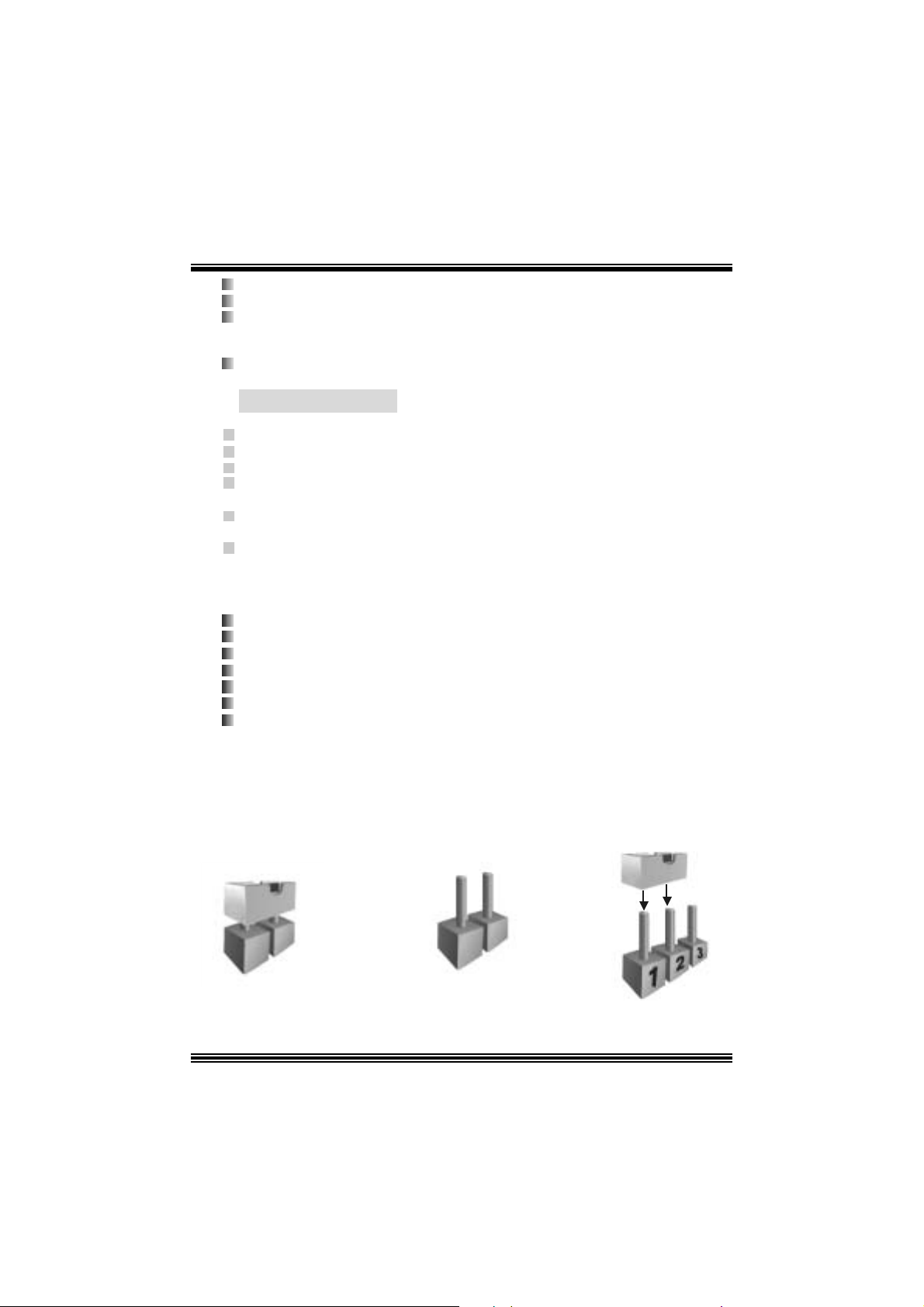
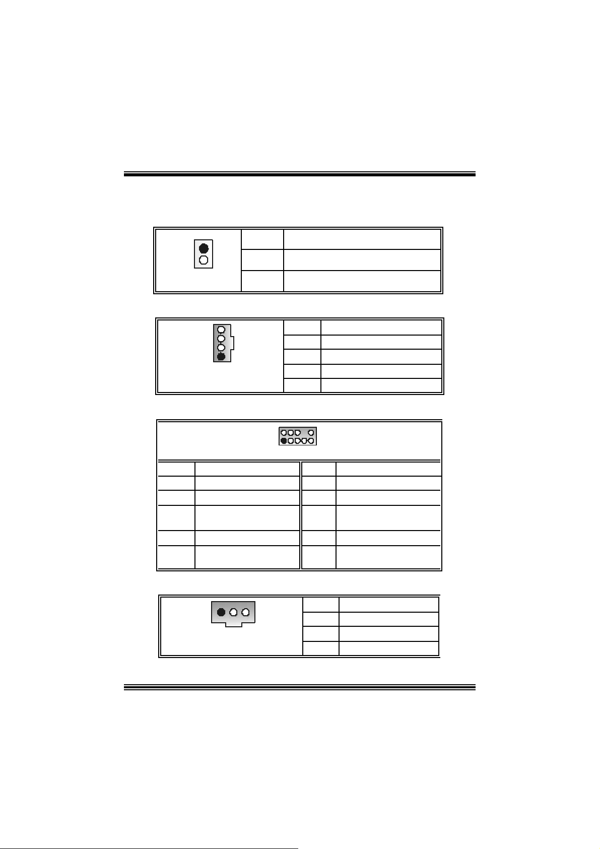
Ho w to setup Jumper
The illustrat ion sho ws how jum pe rs are s e tu p. When the Jum per c ap is placed on pins, the
jumper is “close”. If no jumper cap is placed on the pins, the jumper is ”open”. The
illust rat ion sho ws a 3-pin jumper whos e pin 1and 2 are “close” when jumper c ap is placed
on thes e 2 pins .
Jumper close Jumper open Pin 1-2 close
4

CPU Installation
Step1: Pull the lever sideway s away from the s ock et and then raise the lever up to a
90 -degree angl e.
Step2: Look for the white dot/c ut edge. The whit e dot/cut edge should point towards the
lev er pivot. The C PU will f it only in the c orrect orient ation.
Step3: Hold the CPU down fir ml y, and then close the lever.
Step4: Put t he C PU f an on t he C PU and buck le it. Connect the CPU fan power c able t o
the JCFAN1. This completes the installation.
Step1 Step2 Step3 Step4
CPU Fan Headers: JCFAN1
31
JCFAN1
S ystem Fan Headers: JSFAN1
31
JSFAN1
Pin No. A ssi gnm e nt
1 Ground
2
3
FAN rpm Rate Sense
+12V
Pin No. A ssi gnm e nt
1
2
3
FAN rpm Rate Sense
5
Ground
+12V
DDR DI MM Module s: DDR1/ DDR2
DR AM Access Time: 2.5V Un buff ere d DDR 200/266 MHz Type requ ired.
DRAM Type: 64MB/ 128MB/ 256MB/ 512MB/ 1GB DI MM Module (184 pin)
Total Memory Size wit h Unbuffere d DI MM s
DI MM S ocket
Location
DDR1 64MB/128MB/256MB/512MB/1GB
DDR2 64MB/128MB/256MB/512MB/1GB
DDR Mod u l e To tal Memory
Size (MB)
*1
*1
***On ly for refer en ce***
Max is
2GB
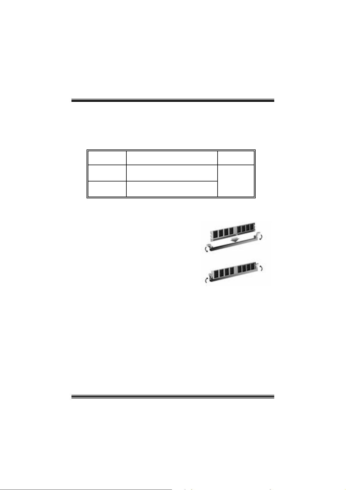
Installing DDR Module
1. Unlock a DIMM slot by pressing the
retaining clips outward. Align a DIMM on
t he s lot s uc h t hat t he no t c h on t he D I MM
ma t ches t he break o n the sl ot .
2. I nsert the DIMM f irmly and vertically into
the s lot until the ret ain ing c hip s nap back in
place and the Dimm is properly seat ed.
Jumpers, Headers, Connectors & Slots
Floppy Disk Connector: FDD1
The mot herboard provides a standard f loppy disk connector that supports 360K,
720K, 1.2M, 1.44M and 2.88M floppy disk types. This connector supports the
prov ided f loppy drive ribbon cables .
Hard Disk Connectors: IDE1/ IDE2
The motherboard has a 32-bit Enhanced PCI IDE Controller that provides PIO
Mode 0~4, Bus Mast er, and Ultra DMA 33/ 66/ 100/ 133 functionality. It has t wo
HDD connec t ors IDE1 (primary) and IDE2 (secondary).
The ID E c onnectors can c onnect a master and a slav e driv e, so you can connect
up t o f our hard disk driv es. The first hard drive s hould alway s be c onnected to
IDE1.
6
0
Peripheral Component Interconnect Slots: PCI 1-3
This m ot herboard is equipped with 3 st andard PCI s lots. PCI stands for Peripheral
Component I nterconnec t, and it is a bus standard for expansion cards. This PCI
slot is des ignated as 32 bits.
Accelerate d Graphics Port Slot: AGP1
Your monitor will attach directly to that video card. This motherboard supports
video cards f or PC I s lots, but it is als o equipped with an Accelerated Graphics Port
(AGP). An AGP c ard will take advantage of AGP technology f or improv ed video
efficiency and perform ance, es pecially with 3D graphics.
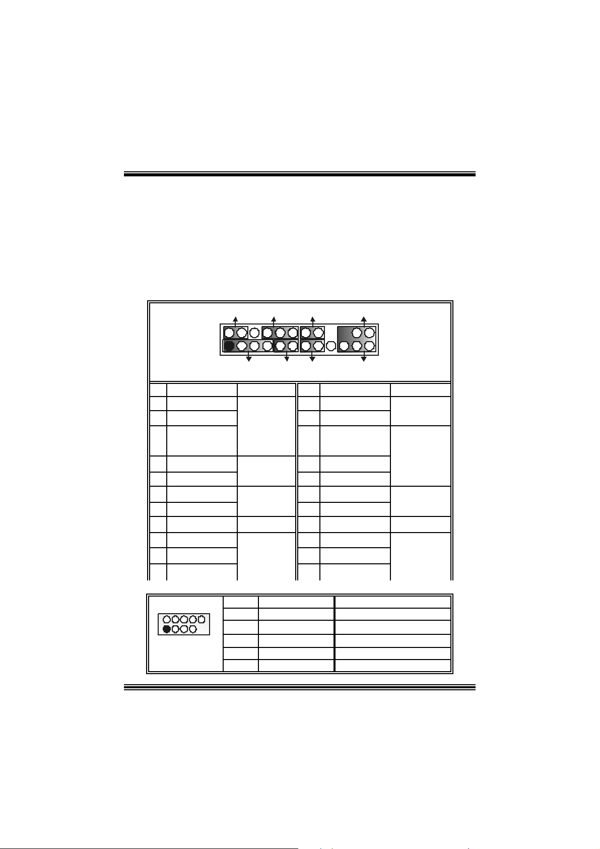
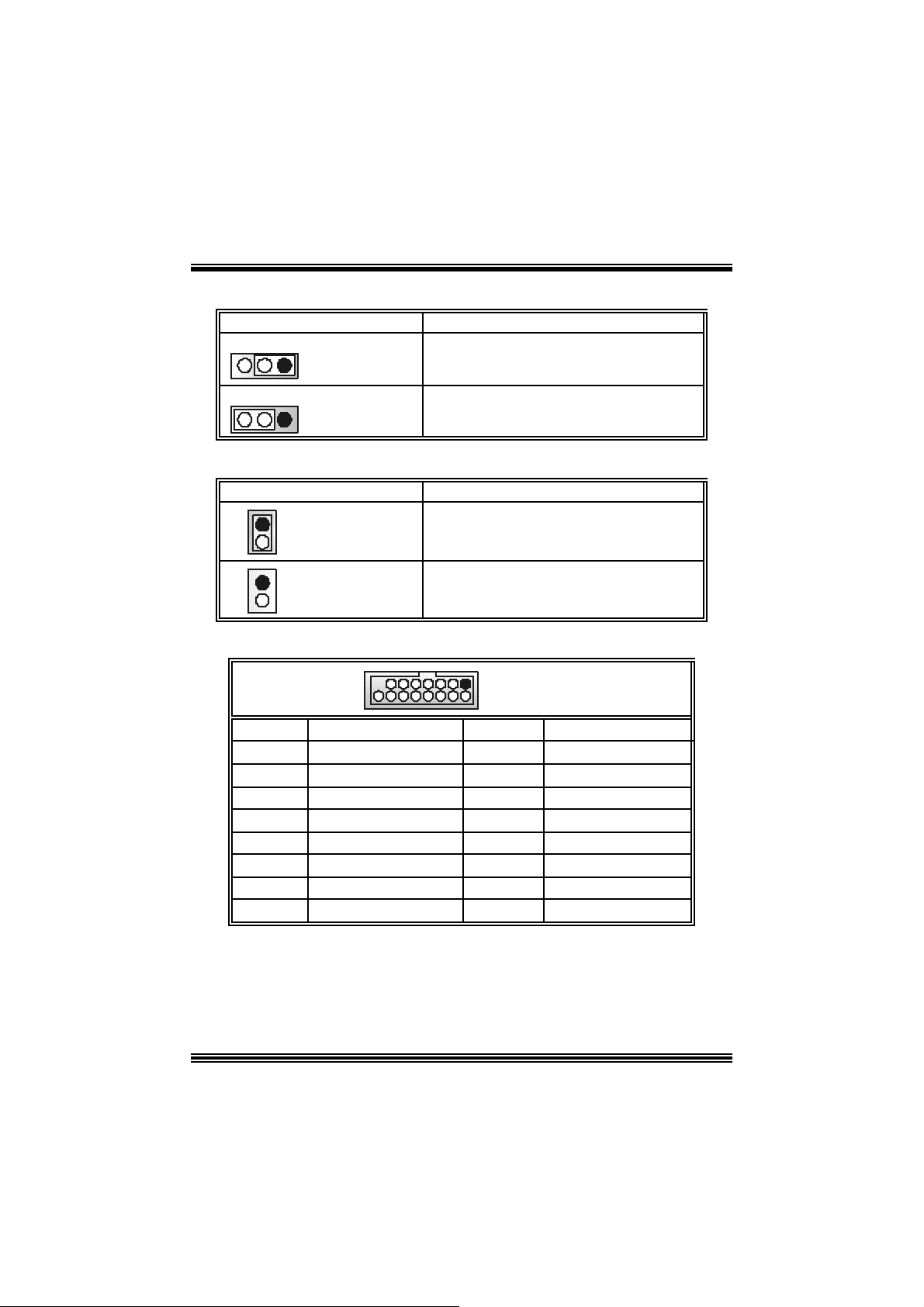
Front Pane l Conne ctor: JPANEL1
SLP
JPANEL1
Pin Assignment Function Pin Assignment Function
1 +5V 2 Sleep C ontrol
3 NA 4 Ground
5 NA 6 NA NA
7 Speaker
9 HDD L E D ( +) 10 Power LED (+)
11 H DD LED (-)
13 Ground 14 Power Button
15 Reset Control
17 NA 18 KEY
19 NA 20 KEY
21 +5V 22 Ground
23 IRTX
2
123
PWR_LED
(+) (-)(+)
SPK
Hard Dr ive
(+) (-)
HLED
RST
Speaker
Connector
8 Power L ED (+)
LED 12 Power L ED (-)
Reset
Button 16 Ground
IrDA
Connector
24 IRRX
IRON/ OFF
IR
24
Sleep
Button
POWER
LED
Power-on
Button
IrDA
Connector
Front USB Header: JUSB3
2
1
JUSB3
Pin Assignment Pin Assignment
1
1
3
9
5
7
9
+5V(fused)
USBP4-
USBP4+
Ground
KEY
2
4
6
8
10
+5V(fused)
USBP5-
USBP5+
Ground
NA
7

Wake On LAN He ader: JWOL1
13
JWOL1
Pin Assignment
1 +5V Standby
2
3 Wak e up
Ground
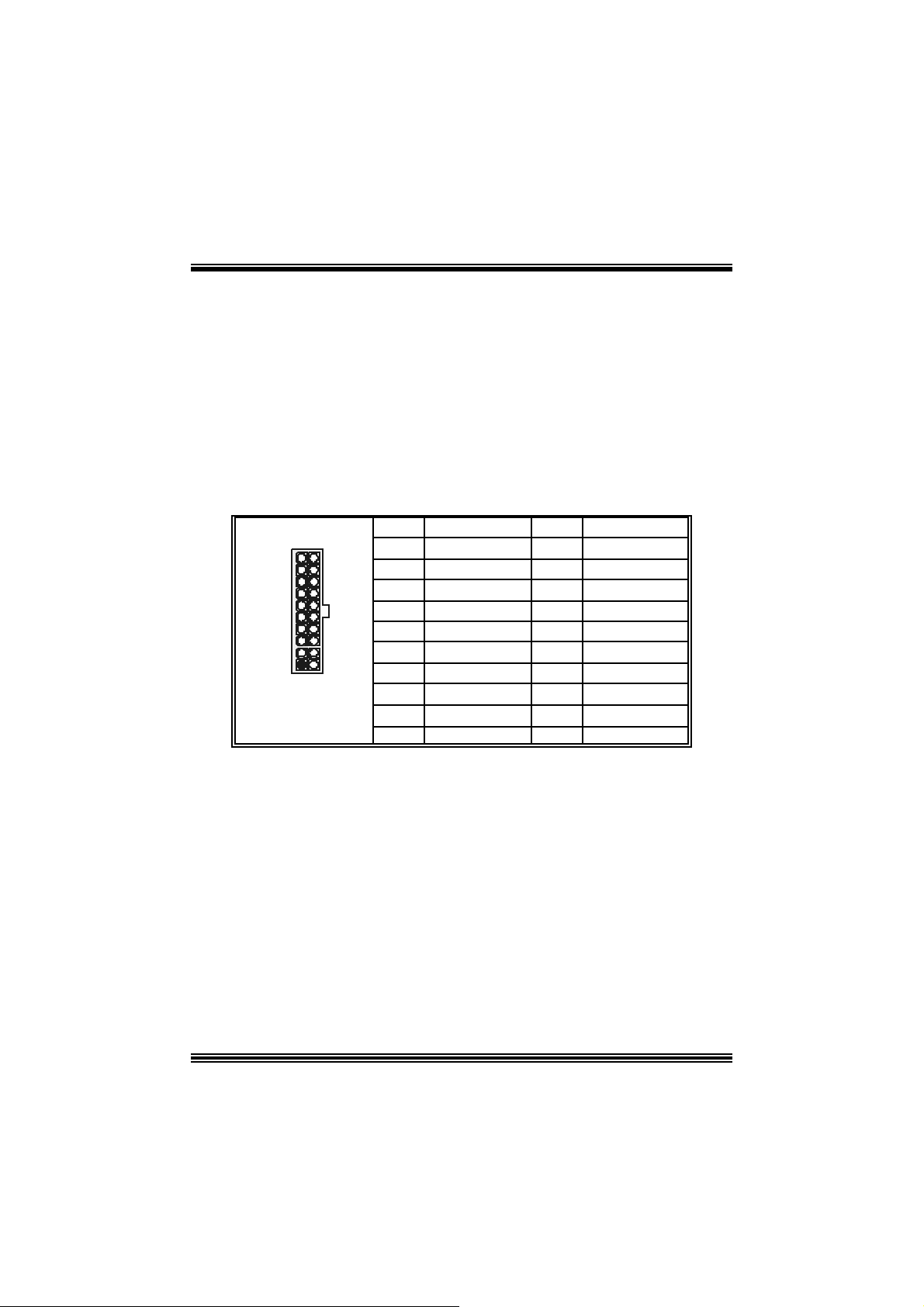
Power Conn ectors: JATXPWER1
PIN Assignment PIN Assignment
1 +3.3V 11 +3.3V
2 +3.3V 12 -12V
3 Ground 13 Ground
4 +5V 14 PS_ON
5 Ground 15 Ground
6 +5V 16 Ground
7 Ground 17 Ground
8 PW_OK 18 -5V
9 Standby Voltage
+5V
10 +12V 20 +5V
19 +5V
20
11
JATXPWER1
10
1
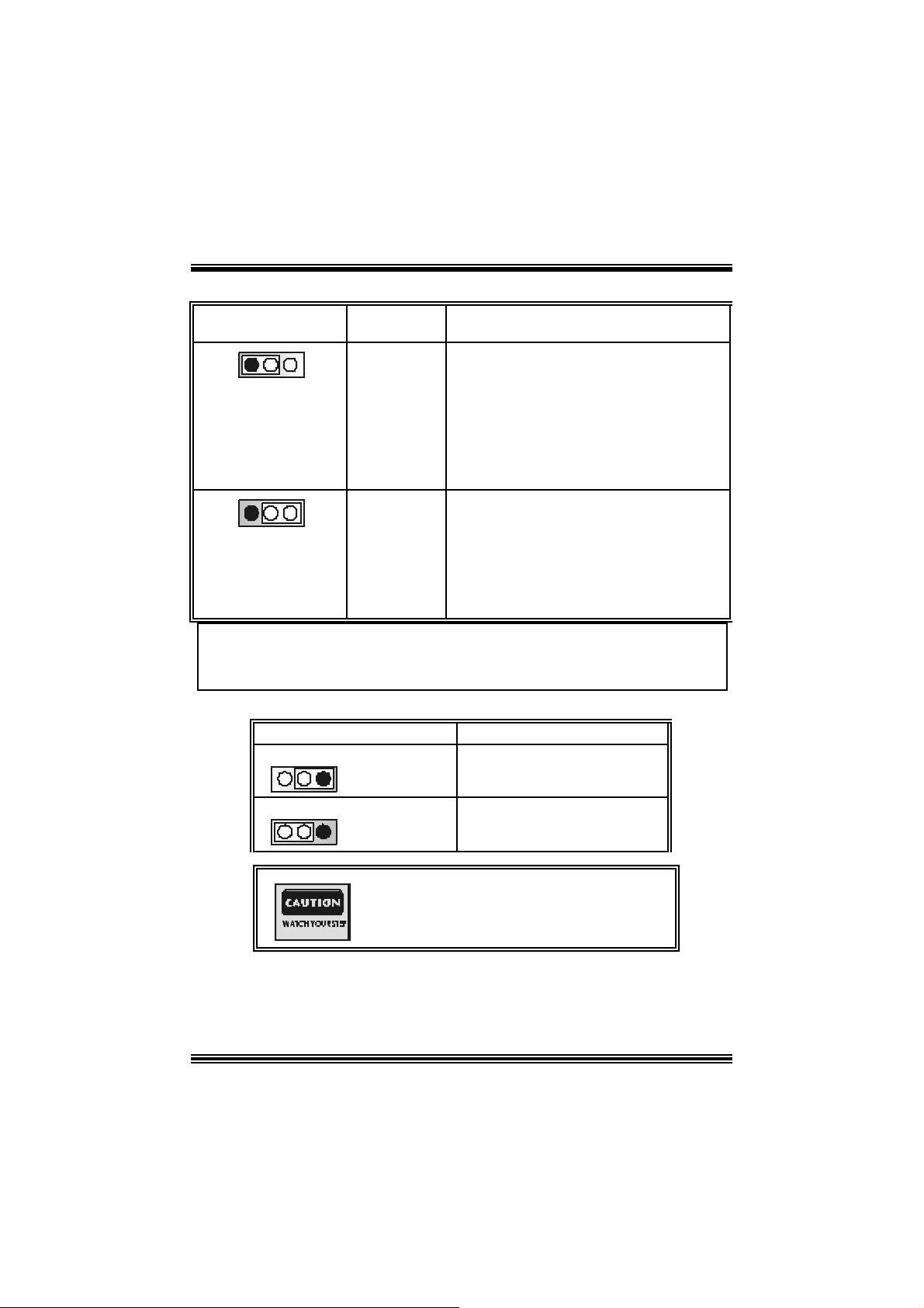
Power Source Selection for Keyboard and Mouse: JKBV1
JKBV1 Assignment Description
1
3
Pin 1-2 close
1
3
Pin 2-3 close
+5V
+5V Standb y
Voltage
+5V for keyboard and mouse
PS/2 Mous e and PS/2 Key board are
powered with +5V standby v oltage
No t e: In o rder to su pport th i s fun cti o n “Pow e r-o n sy ste m v i a ke yb oa rd and
mouse, “J KB V1” jumper cap shoul d be pl aced on pin 2-3.
8
p
Power S our ce Selecti on fo r USB: JUSBV1/ JUSBV2/ JUS BV3
JUSBV1/ JUSBV2/
JUSB V3
Assignment Description
1 3
Pin 1-2 c lose
1 3
Pin 2-3 c lose
+5V
+5V Standby
Voltage
JUSBV2: 5V f or U SB locat ed at the JU SB4
port
JUSBV3: 5V f or U SB locat ed at the JU SB3
port
JU SBV1: 5V for U SB locat ed at the
JU SBLAN1 port
JUSBV2: JU SB4 port powered with standby
volt age of 5V
JUSBV3: JU SB3 port powered with standby
volt age of 5V
JU SBV1: JUSBLAN1 port powered with
st andby volt age of 5V
Note: In orde r to support this functio n “P owe r-on the system via USB device ”,
“JUSBV1/JUSBV2/JUSBV3” jumper cap should be placed on pin 2-3
respectivel y.
Clear CMOS Jumper: JCMOS1
※ Clear CMOS Procedures:
1. R emov e AC power line.
2. Set the jumper to “Pin 2-3 c lose”.
3. Wa it for fi ve seconds.
4. Set the jumper to “Pin 1-2 c lose”.
JCMOS1 Assignment
13
Pin 1-2 Close
13
Pin 2-3 Close
Norm al Operation (def ault)
Clear CMOS Data
The fo llowing procedu res a re for res etting the
BIOS
assword . It is i mportant to follow these
ins truct ions c lose ly.
9
5. Power on AC.
6. R eset your des ired password or clear t he C MOS dat a.
Ca se Op e n Connec tor : JCI 1
Assignment
Case Open Signal
Ground
1
JCI1
Pin
1
2
CD-ROM Audio-In Heade r: JCDIN1
4
1
JCDIN1
Pin Assignment
1
2
3
4
Left Channel In put
Ground
Ground
Right Channel In put
Front Panel Audio Header: JF_AUDIO
2
1
JF_AUDIO
Pin Assignment Pin Assignment
1
3
5
7
9
Mic I n / C e nter
Mic Power/ Bass
Right Line Out/ Right
Speak er Out
Reserved
Left Line Out/ Left
Speak er Out
2
4
6
8
10
10
9
Audio Power
Right Line Out/ Right
Speak er Out
Left Line Out/ Left
Speak er Out
Digital Audio Conne ctor: JSPDIF1
Ground
Key
13
JSPDIF1
Pin Assignment
1
SPDIF_OUT
10
2
3
+5V
Ground
X
CNR Codec/ Onboard Selection: JCODECSEL
JCODECSEL Assignment
13
Pin 1-2 C lose
13
Pin 2-3 C lose
Onboard C odec is used (def ault)
CNR Codec is used
CPU Frequency Selection: JC LK1
JCLK1 Assignment
1
Pin 1-2 Close
1
Pin 1-2 Open
100 MHz
133 MHz
Game Port Header: JGAME1
15
Pin Assign m ent Pin Assignment
1
3
5
7
9
11
13
15
Joy stick B C oordinate X
Joy stick B C oordinate Y
+5V
Joy stick B Butt on 1
MIDI Output
Joy stick B Butt on 2
MIDI Input
NA
1
216
JGAME1
2
4
6
8
10
12
14
16
Joy st ick A Coordinate
Joy st ick A Coordinate Y
Joystick A Button 1
Joystick A Button 2
+5V
Ground
Ground
+5V
11
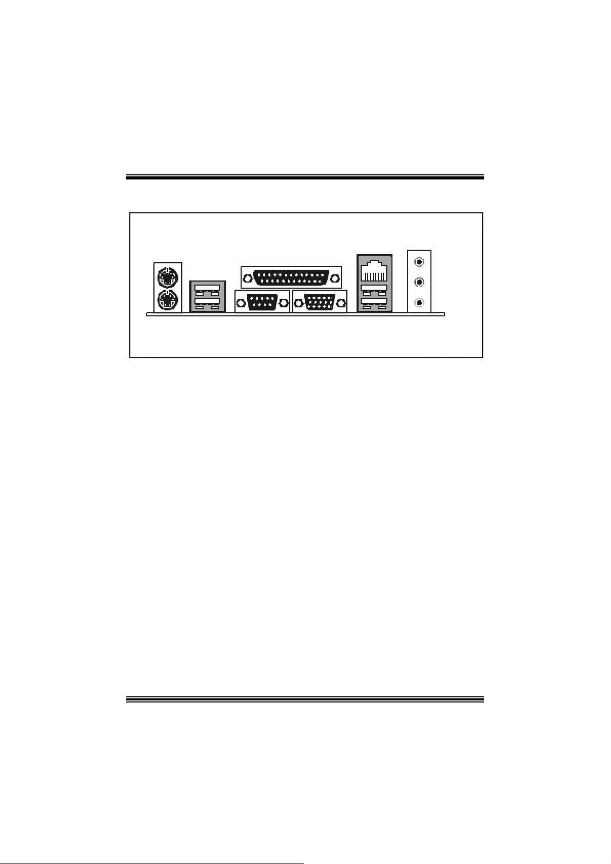
B ack Panel Connectors
JKBMS1
JKBMS1
PS/2
PS/2
Mous e
Mous e
JUSB4
JUSB4
JPRNT1
JPRNT1
Parallel
Parallel
JUSBLAN1
JUSBLAN1
LAN
LAN
Li ne In
Li ne In
Speaker
Speaker
Out
Out
Mic In
Mic In
PS/2
PS/2
Keyboard
Keyboard
USB
USB
COM1
COM1
JCOM1
JCOM1
VGA1 USB
VGA1 USB
JVGA1
JVGA1
JAUDIO
JAUDIO
12

Deutsch
Spezifikatione n von M7VIG Pro-D
A. Har dware
CPU
Unterstützung für Sockel A.
Unterstützung für die AMD® Athlon/(ThunderbirdTM) /A thlonTM XP/DuronTM
Prozessoren
F SB mit 200/ 266MHz.
Chipsatz
N orthbridge: VI A KM266.(VT8375)
Sout hbridge: VIA KT8235.
Hauptspeicher
Unter stützung fü r 2 DDR Ge räte.
Unterstützung für 200/266 (ohne ECC) DDR Gerät e
D ie m ax imale Speichergröße ist 2GB.
Super I/O
Chip: Winbond W83 697H F.
Steckplätze
Drei 32-bit PCI-Bus-Slot s.
Ein AGP-Slot. (1x/ 2x/ 4x)
Onboard-IDE
Unterstützung fü r vi er IDE Diskettenl au fwe rke.
U nterstüt zung für PIO Modus 4, Mas t er Modus und Ultra DMA 33/66/100/133 Bus
Mast e r Mo dus .
Onboard AC’97 Sound Codec
C hip: VIA VT1612A.
Entspricht die Spezifikation v on A C’97.
Unterstützung für 2-Kanal.
Onboard-Peripheriegeräte
a. Für Rückw and
1 serielle Schn it tst elle.
1 VGA-Schnittstelle.
1 parallele Sc hnittstelle. (SPP/EPP/EC P-Modus )
Audio Schnittst ellen in vert ikale Stellung.
1 LAN -Buchs e.
Uerstützung f ür PS/2-Maus und PS/2-Tastatur.
4 U SB 2.0-Ports.
13

b . Für Vo rd erse i te
1 Floppy -Port mit Unters t ützung f ür 2 Diskettenlauf werke.(360KB, 720KB, 1.2MB,
1.44MB und 2.88MB)
2 USB 2.0- Ports.
1 Front –Audio-Hea der.
Abmessungen
Mic ro ATX Form -F act or: 21.3 X 24.4cm (W X L)
B. BIOS & S oftware
BIOS
Award legal Bios .
Unterstützung für APM1. 2.
Unterstützung f ür ACPI.
Unterstütz ung für U SB Funkt ion.
Software
Unterstützung für Warpspeed erTM, 9th TouchTM, FLASHER™, Win Flasher
StudioFun!
Unter stützung für die am mei s ten verbreiteten Be triebsyste me wie Wi ndows 98SE,
Windows 2000, W indows ME, Windows XP und SC O UNIX usw.
TM
. (optional)
TM
Verpackungsinhalt
HDD K a b le X1
FDD Kable X1
Benut zer Handbuch X1
USB Kable X1 (optional)
I/O-Rückwand f ür ATX Gehäuse X1 (optional)
Treiber C D für Installation X1
S/ PD IF-Kable X1 (optional)
und
Ei nst e l lu ng de r Jum per
Die Abbildung verdeutlicht, wie Jumper eingestellt werden. Pins werden durch die
Jum per-Kappe v erdeckt, ist der Jum per ”geschlossen”. Keine Pins werden durch die
Jum per-Kappe verdeckt, is t der Jum per “geöffnet”. Die Abbiildung zeigt einen 3-Pin
Jumper dessen Pin1 und Pin2 ”geschlossen“ sind, bzw. es befindet sich eine
Jum per-Kappe auf dies en beiden Pins.
Jumper geschlossen Jumper geöffnet Pin1-2 geschlossen
14
In stallat ion der CPU
Sc hritt 1 : Z iehen Sie den H ebel s eitlich vom Sockel weg. Heben Sie den Hebel dann
in 90-Grad-Winkel nac h oben.
Sc hritt 2 : Suchen Sie nac h der scharfen Kant e, die auf D rehpunkt des Hebels
weisen m uss . Die CPU passt nur, wenn s ie ric htig aus geric ht et ist.
Sc hritt 3 : D rück en Sie die CPU f est in den Sock el und s c hließ en Sie den Hebel.
Sc hritt 4 : Ste cken Sie Ih ren CPU-Lüf ter auf die CPU. Schließen Sie die Stromversorgung sstecker
CPU- Lüfter Headers: JCFAN1
für CPU -Lüft er an JCFAN1 an. D ann beenden Sie die Installat ion.
Schritt 1 Schritt 2 Schritt 3 Schritt 4
Pin
1
2
JCFAN1
31
3
System-Lüfter Headers: JSFAN 1
31
JSFAN1
Pin
1
2
3
Belegung
Masse
+12V
FAN R PM G eschwindigkeit Sens or
Belegung
Masse
+12V
FAN R PM Geschwindigkeit Sens or
15

DDR- DIMM-Mo dule s: DDR1/ DDR2
DR AM-Z ugriffszeit: 2. 5V unbuf fered DDR 200/ 266 MH z Ty p erforderlic h.
DR AM Ty pen: 64MB/ 128MB/ 256MB/ 512MB/ 1GB D IMM-Module (184-Pin)
Gesa m t Spei che rgröße v on ni cht reg is trierte r DIMM s
DIMM-Sockel
Standort
DDR1 64MB/128MB/256MB/512MB/1GB
DDR2 64MB/128MB/256MB/512MB/1GB
DDR-Modul Speichergröße
*1
*1
**Nur als Refer enz***
Maximal
2 GB
Installation von DDR-Modul
1. Öff nen Sie einen DIMM-Slots, indem Sie
die seitlich Chips nach außen drücken.
Ric ht en Sie das D I MM-Modul so über dem
Slot aus, dass das Modul mit der Kerbe in
den Slot passt.
2. D rücken Sie das DI MM-Modul in den Slot,
bis die seitlic hen Clips zuschnappen und
das Modul fest sitzt.
Jumpers, Headers, Anschlüsse & Slots
Diskettenanschluss: FDD1
Das Motherboard enthält einen st andardmäßigen Diskettenans chluss, der 360K-,
720K-, 1.2M-, 1.44M- und 2.88M-Disketten unterstützt. Dieser Anschluss
unt ers tützt die mit gelief erte Bandkabel des Diskettenlauf werks.
Fe stplatt enanschlüsse: IDE1 und ID E2
Das Mainboard hat einen 32-Bit Enhanced PCI IDE-Controller, der die Modi
PIO0~4, Bus Mast er sowie die U ltra DMA/33/ 66/100/133- Funkt ion zur Verfügung
stellt. Dieser ist mit zweii HDD-Anschlüssen versehen IDE1 (primär) und IDE2
(sekundär).
Die ID E-Anschlüsse k önnen eine Master- und eine Slav e-Festplatte v erbinden, so
dass bis zu 4 Festplatten angeschlossen werden können. Die erste Festplatte
sollte im m er an IDE1 angeschlossen werden.
16
Periphera l Comp onent Int erconnect Slots: P CI1-3
Dieses Motherboard ist m it 3 standardmäß igen PCI-Slots ausgestattet. PC I steht
für Peripheral Component Interc onnect und bezieht sich auf einem Busst andard für
Erweiterungskarten, der den älteren ISA-Busstandard in den meisten
Schnittst ellen ers etzt hat. Dieser PCI-Slot ist f ür 32 bits v orgesehen.
Accelerate d Graphics Port Slot: AGP1
Ihr Monitor wird direkt an die Grafikkarte angeschlossen. Dieses Motherboard
unterstützt Grafikkarten f ür PCI-Slots, aber es ist auch mit einem Accelerated
Graphic s Port ausgestattet. AGP-Karten verwenden die AGP-Technologie, um die
Wirks amk eit und Leistung v on Videosignalen zu v erbessern, besonders wenn es
sich um 3D-Graf iken handelt.
Stromversorgungsanschluss: JATXP WER1
PIN Belegung PIN Belegung
1 +3.3V 11 +3.3V
2 +3.3V 12 -12V
3 Masse 13 Masse
4 +5V 14 PS_ON
5 Masse 15 Masse
6 +5V 16 Masse
7 Masse 17 Masse
8 PW_OK 18 -5V
9 +5V_SB 19 +5V
10 +12V 20 +5V
10
1
JATXPWR1
20
11
17
Anschlüsse für die Vo rderseite: J PANEL1
SLP
JPANEL1
Pin Belegung Funktion Pin Belegung Funktion
1 +5V 2 Sleep Control
3 Kein 4 Masse
5 Kein 6 Kein Kein
7 Lautsprecher
9 HDD LED (+) 10 Po w er L ED ( + )
11 HDD LED (-)
13 Masse 14 Power-Knopf
15 Reset Control
17 Kein 18 Schlüsse Kein Pin
19 Kein 20 Schlüsse
21 +5V 22 Masse
23 IRTX
* S ch l ü ss e : Kei n P i n.
2
123
PWR_LED
(+) (-)(+)
SPK
(+) (-)
HLED
RST
Lautsprecher
Anschluss
8 P ower L ED ( +)
Festplatte
LED 12 Power LED (-)
Zurücksetzn-
Knopf
IrDA-
Anschluss
16 Masse
24 IRRX
IRON/ OFF
IR
24
Schlafen-
Knopf
Power-
LED
Power-On
Knopf
IrDA
Anschluss
Front USB Header: JUSB3
2
1
JUSB3
10
9
Pin
1
3
5
7
9
Belegung
+5V(geschmelzt)
USBP4-
USBP4+
Masse
Schlüsse
Pin
2
4
6
8
10
Belegung
+5V(geschmelzt)
USBP5-
USBP5+
Masse
Kein
Wake On LAN He ader: JWOL1
13
JWOL1
Pin
1 +5V res erv ierte Spannung
2
3 Aufwecken
Belegung
Masse
18

Auswahl von Stromsmodi für Tastatur/ Maus: JKBV1
JKBV1 Belegung Beschreibung
1
3
Pin 1-2 gesc glossen
1
3
Pin 2-3 gesc hlossen
Anmerkung: Um die Funktion
aktivieren, müs s en Pins 2-3 von JKBV1 durch die Jumperkappe verdeckt werden.
+5V +5V für Tas tatur und Mau s
+5V reservierte
Spannung
―
Durch +5V reservierte Sapnnung für
PS/ 2-Tast atur und PS/2-Maus zum
Erwecken von dem System
Erwecken durch Tastatur/Maus ― zu
Auswahl von Stromsmodi für USB: JUSBV1/ JUSBV2/ JUS B V3
JUSB V1/JUSB V2/
JUSBV3
1 3
Pin 1-2 gesc hlossen
1 3
Pin 2-3 gesc hlossen
Anmerkung: Um die Funktion
Pins 2-3 v on JUSBV1/J U SBV2/JUSBV3 durc h die J umperkappe verdec kt werden.
Belegung Beschreibung
JUSBV1: +5V f ür den USB-Port von
JUSBLAN1
+5V
+ 5V re s erv i ert e
Spannung
―
Erwecken durc h USB ― zu aktivieren, müssen
JUSBV2: +5V f ür den USB-Port von
JUSB4
JU SBV3: +5V f ür f ür den U SB-Port v on
JUSB3
JU SBV1: +5V reserv iert e Sapnnung f ür
den USB-Port von JUSBLAN1
zum Erwecken
JU SBV2: +5V reserv iert e Sapnnung f ür
den USB-Port v on J USB4 zum
Erwecken
JU SBV3: +5V reserv iert e Sapnnung f ür
den USB-Port v on J USB3 zum
Erwecken
19

Jumper zum Löschen CMOS: JCMOS1
JCMOS1
13
Pin 1-2 gesc hlossen
13
Pin 2-3 gesc hlossen
Beschreibung
Normale Operation (Default )
CMO S-Daten Lös chen
Die folgend e Schritte leiten Si e, das Kennwort für
BIOS -System zurückzusetzen. Es ist wichtig, die
Anweisung zu folgen.
※ Prozeß zum Löschen des CMOS:
1. Aussc halten Sie das Syst em.
2. Lassen Sie Pin 2-3 von JC OMS1 ges hclossen sein.
3. Bitte wart en Sie 15 Sekunden.
4. Lassen Sie Pin 1-2 von JC OMS1 ges hclossen sein.
5. Einschalten Sie das System wieder.
6. Zurücksetzen Sie ihr gewunschtes Kennwort oder löschen Sie die
CMOS-Daten.
Warnmeldung für Chassis-Öffnen Anschluss: JCI1
1
JC1
Pin
1
2
Belegung
Gehäus e Öffnen Signal
Masse
CD-ROM Audio-In Heade r: JCDIN1
4
1
Pin Belegung
1
2
Link-Kanal Eingabe
JCDIN1 3
20
Masse
Masse
4 Recht -Kanal Eingabe
Front Panel Audio Header: JF_AUDIO
2
1
JF_AUDIO
Pin Belegung Pin Belegung
Mikrofon-Eingabe/Z entrum
1
Mikrofon-Betriebsspannung/B
3
ass
5
Audio-Signal des rechten
Kanals zurVorderseit e /
Lautsprecher-Signal des
rechten Kanals zur Vorderseite
Reservie r et fü r sp ä t.
7
Ve rwend ung d urc h
Kopfhörer-Verst ärker
Audio-Signal des linken
9
Kanals zur Vorderseite /
Lautsprecher-Signal des
linken Kanals zur Vorderseit e
*R es erviert: N icht in Gebrauc h
10
9
Masse
2
4 Audio-Betriebsspannung
Audio-Signal des recht en
Kanals zur Vorderseite /
6
Laut s prec her-Signal des
rec ht en Kanals zur
Vorderseite
Schlüsse
8
Audio-Signal des linken
Kanals zur Vorderseite /
10
Laut s prec her-Signal des
link en Kanals zur Vorderseite
Digital Audio A n schluss: JSP D IF1
13
JSPDIF1
Au swahl Onboard /CNR -Codec : JCODE CSEL
JCODECSEL Beschreibung
13
13
Pin Belegung
1 +5V
2
3
Verwendung von Onboard-Codec
Pin 1-2 ges c hloss en
Pin 2-3 ges c hlossen
21
SPDIF_Ausgabe
Masse
(Default)
Verwendung von CNR-Codec
CPU Frequenz Auswahl: JCLK1
JCLK1 Beschreibung
1
Pin 1-2 gesc hlossen
100MHZ
1
Pin 1-2 geööff net
Game Header: JGAME1
15
Pin Belegung Pin Belegung
1
3
Joystick B Koordierung X
5
7
Joystic k B Koor dierung Y
9
11
13
15
+5V
Joy stick B Knopf 1
MIDI Ausgabe
Joy stick B Knopf 2
MIDI Eingabe
Kein
1
216
2
4
6
8
10
12
14
16
Anschlüsse für die Rückwand
JKBMS1
PS/2Maus
PS/2 Tastat ur
JUS B4
USB
COM1
JCOM1
JPRNT1
Parallel
VGA1 USB
JVGA1
JUSBLAN1
133MHz
+5V
Joystick A Knopf 1
Joy stick A Koordierung X
Masse
Masse
Joy stick A Koordierung Y
Joystick A Knopf 2
+5V
LAN
Lin e In
Speaker O ut
Mic I n
JAUDIO
22

WarpSpeeder
Introduction
[ W arpSpeeder™ ], a new powerf ul control utility, f eatures three us er-f riendly functions
including Ov erclock Manager, Ov ervoltage Manager, and H ardware Monit or.
With the Over clock Manage r, users can easil y adjust the frequency the y prefer or they can
get t he best CPU perf ormanc e wit h jus t one click . The Ov ervoltage Manager, on the other
hand, helps to power up CPU core voltage and Memory voltage. The cool Hardware
Monitor smartly indic ates the t emperatures, volt age and CPU fan speed as well as the
chips et inform at ion. Also, in t he About panel, you c an get det ail des c ript ions about BI OS
model and chipsets. In addition, t he frequency status of CPU, memory, AGP and PC I
along with t he C PU s peed are synchronically shown on our m ain panel.
Moreov er, to protect users' com puter syst em s if the s etting is not appropriat e when testing
and results in system f ail or hang, [ WarpSpeeder™ ] technology assures the system
st ability by automat ically reboot in g the c om puter and then restart t o a speed that is either
the original sys t em speed or a s uit able one.
System Requirement
OS Support : Windows 98 SE, W indows Me, Windows 2000, Windows XP
Direc t X: DirectX 8.1 or abov e. (The W indows XP operating sys tem inc ludes D irectX 8. 1. If
you us e W indows XP, y ou do not need t o inst all D irectX 8. 1. )
23
 Loading...