

Page 1

M7VIB Ver:2.5&2.6
Federal Communications Commission
(F.C.C) Statement
T his device complies with Part 15 of the FCC Rules. Operation of this device is
subject to the following two conditions : (1) this device may not cause harmful
interference, and (2) this device must accept any interference rece ived, inc luding
interference that may cause undesired operation.
Accessories : T his de vice h as been test ed and f ound to co mp ly with the lim its of a
Class B digital device; the accessories associated with this equ ipment are as
fol lows :
1. Shielded seria l cable. (Can be obtained from multiple retail outlets)
2. Shielded prin ter cable. (Can be obtained from multiple retail out lets)
3. Shielded video cable. (Can be obtained from multip le retail outlets)
4. Shielded power cord. (Provided by manufacturer)
These accessories are required to ensure compliance w ith FCC Rules. It is the
responsibility of the user to provide and use these accessories properly.
This equipment has been tested and found to comply with the limits of a Class B
digital device, pursuant of Part 15 of the FCC Rules. These limits are designed to
provide reasonab le protection against harmful interference in a residential
installat ion. This equipment generates, uses and radiates radio frequency energy
and, if you did not installed and used in accordance with the instructions, may cause
harmful interference in the radio communications. There is no guarantee that
interference will not occur in a particular installation. If this equipment does cause
harmful interference in the radio or television reception, which can be determined
by turning the equipment off and on, you are encouraged to try to correct the
interference by one or more of the followin g measures :
1. Reorient / relocate the receiving antenna.
2. Increase the separation between the equipment and the receiver.
3. Connect the equipment into an outlet from a different circuit where the
receiver is connected.
4. Consult the dealer or an experienced radio/TV technician for help.
Caution: Changes or modifications that is not expressly approved by the
manufacturer could void the user’s authority to operate the equipment.
Page 2

Disclaimer
The vendor makes no representations or warranties with respect to the contents
here of and specially the vendor disclaims any implied warranties of
merchantability or fitness for any purpose. Further, the vendor reserves the right to
revise this publication and to make changes of the contents here of without
obligation to notify any party beforehand.
Duplication of this publication, in part or in whole, is not allowed without first
obtaining the vendor’s approval in writing.
Trademarks and Remarks
MS-DOS, Windows, Windows NT , Windows 9X, Windows ME, Windows XP
and Windows 2000 are products of Microsoft Corp, with its ownership of
trademark, and are distributed by the vendor under a license agreement.
All trademarks used in this manual are property of their respective owners.
Co pyright© 2001
All Rights Reserved
Canadian D.O.C. Statement
This digital apparatus does not exceed the Class B limits for radio noise emissions
from digita l apparatus to set out of the radio interference regulations of the
Canadian Department of Communications.
Cet appareil numérique n‘émet pas de bruits radioélectriques dépassant les limites
appliquées aux appareils numériques de Class B préscrits dans le réglement du
brouillage radioélectrique edict par le minister Des Communications du Canada.
Page 3

Contents
Introduction .................................................................................. 1-1
1. Motherboard Description........................................................ 1-2
1.1 Features ....................................................................................................1-2
1.1.1 Hardware....................................................................................................................1-2
1.1.2 BIOS ...........................................................................................................................1-5
1.1.3 Software......................................................................................................................1-5
1.1.4 Accessories ................................................................................................................ 1-5
1.2 Motherboard Installation..........................................................................1-6
1.2.1 System Block Diagram ........................................................................................... 1-6
1.2.2 Layout of Motherboard ...........................................................................................1-7
1.2.3 Quick R eference .......................................................................................................1-8
1.3 CP U Installatio n.......................................................................................1-9
1.3.1 CPU Installation Procedure: Soc ket A .................................................................1-9
1.3.2 Frequency Selection: JCLK1 ...............................................................................1-10
1.3.3 CPU Fan Header: JCFAN1 ..................................................................................1-10
1.3.4 System Fan Header: JSFAN1..............................................................................1-11
1.3.5 North Bridge Chipset Fan Header: JNFAN1....................................................1-11
1.4 RAM Module Installation ......................................................................1-12
1.4.1 DIMM.......................................................................................................................1-12
1.4.2 How to install a DIMM Module..........................................................................1-13
1.5 Slots........................................................................................................1-14
1.5.1 ACR (Advanced Communication Riser) Slot..................................................1-15
1.5.2 AGP (Accelerated Graphics Port) Slot...............................................................1-15
i
Page 4

Contents
1.5.3 CNR (Communication Network Riser) Slot.....................................................1-15
1.5.4 PCI (Peripheral Component Interconnect) Slots ..............................................1-15
1.6 Co nnectors, Headers & Jumpers............................................................1-16
1.6.1 Front Panel Connector: JPANEL1......................................................................1-17
1.6.2 AT X 20-pin Power Connec tor: JATXPWR1..................................................1-19
1.6.3 Hard Disk Connectors: IDE1/IDE2....................................................................1-19
1.6.4 Floppy Disk Connector: FDD1 ...........................................................................1-20
1.6.5 Wake On LAN Header: JWOL1 ........................................................................1-20
1.6.6 Clear CMOS Jumper: JCMOS1..........................................................................1-20
1.6.7 Front USB Header: JUSB2 ..................................................................................1-21
1.6.8 CNR Cod ec Primary/Secondary Selection: J2 .................................................1-21
1.6.9 DDR DIMM Voltage: J9......................................................................................1-21
1.6.10 5V/ 5VSB Selection for USB: JUSBV1 .........................................................1-22
1.6.11 5V/ 5VSB Selection for KB: JKBV1 ..............................................................1-22
1.7 Peripheral Port .......................................................................................1-23
1.7.1 PS/2 Mouse / Keyboard Connector: JKBMS1.................................................1-23
1.7.2 USB Connector: JUSB1 .......................................................................................1-24
1.7.3 Serial and Parallel Interface Ports ........................................................................1-25
1.7.3.1 The Serial Interface: JCOM1/ JCOM2 .............................................1-25
1.7.3.2 Parallel Interface Port: JPRNT1 ......................................................1-27
1.7.4 Game (Joystick/MIDI) Port Connector: J8.......................................................1-28
1.7.5 Audio Port Connectors: J8....................................................................................1-28
1.7.6 Audio Subsystem....................................................................................................1-29
1.7.6.1 CD-ROM Audio-In Header: JCDIN1...............................................1-30
ii
Page 5

Contents
1.7.6.2 CD-ROM Audio-In Header: JCDIN2...............................................1-30
1.7.6.3 Front Panel Audio Header: JAUDIO1..............................................1-30
1.7.6.4 Telephony Audio Header: JT AD1 ...................................................1-30
2. BIOS Setup................................................................................ 2-1
2.1 Main Menu...............................................................................................2-3
2.2 Standard CMOS Features ........................................................................2-6
2.3 Advanced BIOS Features.........................................................................2-9
2.4 Advanced Chipset Features....................................................................2-13
2.5 Integrated Peripherals ............................................................................2-17
2.6 Power Management Setup .....................................................................2-22
2.7 PnP/PCI Configurations .........................................................................2-27
2.8 PC Health Status ....................................................................................2-30
2.9 Frequency/Voltage Control....................................................................2-31
3. Trouble Shooting ...................................................................... 3-1
iii
Page 6

Chapter 1 M otherboard Description
Introduction
System Overview
Co ngratula t ions o n the pur chase of your n ew sys tem! T his mothe rboard is designed to
take advantage of the latest industry technology to provide you with the ultimate
solution in data processing. In the tradition of its predecessors, this motherboard
continues the commitment of reliability, performance and strives for full compliance
and compatibility with industry software and hardware standards.
M7VIB Highlights:
8 Contains on board I/O facilities, which include two serial ports, a parallel port, a PS/2
mouse port, a PS/2 keyboard port, audio ports, USB ports and a game port.
8 Contains on board IDE facilities for IDE devices such as hard disks and CD-ROM
Drives.
TM
8 Supports the AMD-Athlon
you the latest technology in m icroarchitecture design, graphics performance, system
bus design, cache architecture and much more.
8 Complies with PC ATX form factor specifications.
8 Supports popular operating systems such as Windows 95/98, Windows NT, Windows
2000, Windows ME, Windows XP, Novell, UNIX, LINUX and SCO UNIX.
pro cess or, a leadin g ed ge proces sor w hich brin gs to
1-1
Page 7

Chapter 1 M otherboard Description
1. Motherboard Description
1.1 Features
1.1.1 H ardw are
CPU
− Single Socket-A for an AMD Ath lon Family processor.
− Runin g at 100 or 133 MHz Front Side Bus frequency.
− The AMD Athlon system bus supports the 200/266 MHz high-speed,
split-transaction AMD Ath lon system bus interface.
Speed
− Supports up to AMD Athlon
− Supports up to AMD Athlon
− Supports up to AMD Duron
− The 33MHz 32 bit PCI 2.2 compliant.
− The 66MHz AGP 2.0 compliant interface supports 1x, 2x and 4x data
transfer mode.
− High-speed memory --The VT8366/A system controller is designed to
support 200/266 MHz DDR SDRAM DIMMs.
TM
XP 2000+ CPU core speeds.
TM
1.4 GHz CP U core speeds.
TM
1.2 GHz CPU core speeds.
Chipset
− Chipset – VIA VT8366/A and VT 8233A.
− Chipset – Winbond W83697HF.
DRAM Me mo ry
− Supports 64MB/128MB/256MB/512MB/1GB DIMM modules (4).
− Supports DDR (Double Data Rate) Synchronous DRAM (2.5 V).
− Supports 8 banks up to 4Gb DRAMs for registered DDR SDRAM
mo dule. (DIM M x 4p cs)
− Supports 6 banks up to 3Gb DRAMs for unbuffered DDR SDRAM
mo dule. (DIM M x 3p cs)
− 200/266 MHz Bus Frequency.
1-2
Page 8

Chapter 1 M otherboard Description
Shado w RAM
− Motherboard is equipped with a memory controller providing shadow
RAM and su pport fo r 8 bit ROM BIOS.
Green Functionality
− Supports Award BIOS™ power management functionality.
− Has a power down timer from 1 to 15 minutes.
− Wa kes from pow er saving sleep mode with any ke yboa rd or mouse
ac tivity.
BUS S lots
− (1) AGP slot.
− (1) CNR slot (Support Type B CNR only).
− (1) ACR slot
− (5) 32-bit PCI bus slots
Flas h Memo ry
− Supports flash memory functionality.
− Supports ESCD functionality.
Built in IDE Facilities
− Supports four IDE hard disk drives.
− Supports PIO Mode 4, Master Mode, and high performance hard disk
drives.
− Supports disk transfer rates up to 100 MB/second.
− Supports Ultra DMA 33, Ultra DMA 66, Ultra DMA 100, Ultra DMA
133 Bus Master Modes.
− Supports IDE interface with CD-ROM.
− Supports high capacity hard disk drives.
− Supports LBA mode.
Ste reo AC 97 Digital Audio Codec
− Single ch ip audio CODEC with h igh S/N ratio (>90dB).
− 18-bit ADC and DAC resolution.
− Compliant with AC’97 2.2 specification.
− Meet performance requirements for audio on PC2001 systems.
− 18-bit stereo full-duplex CODEC with independent and variable
sampling rate.
1-3
Page 9

Chapter 1 M otherboard Description
− 3D Stereo Enhancement.
I/O facilities
− On e multi- mode Parallel Po rt ca pable of supp ortin g the follow in g
specifications :
Standard & Bidirection Parallel Port.
Enhanced Parallel Port (EPP ).
Extended Capabilities P ort (ECP).
Normal
− Supports two serial ports, 16550 UART.
− Supports Infrared Data Transmission using IrDA.
− Supports PS/2 mouse and PS/2 keyboard.
− Supports 360KB, 720KB, 1.2MB, 1.44MB, and 2.88MB floppy disk
drives.
Universal Serial Bus
− Supports two back panel Universal Serial Bus P orts and two front panel
Universa l Serial Bus Ports (optional).
− Supports 48 MHz USB.
Hardwa re Mo nitor Func tio n
− Monitors CPU Fan Speed.
− Mo nitors S ystem Volta ge.
Dimensions (ATX form-fac to r)
− 24.4cm x 30.5cm (WxL)
1-4
Page 10

Chapter 1 M otherboard Description
1.1.2 B IOS
− AW ARD legal BIOS.
− Supports AP M1.2.
− Supports USB Function.
− Supports ACP I.
1.1.3 Software
Operating System
− Offers the highest performance for MS-DOS, Windows NT, Windows
2000, Windows 95/98, Windows ME, Windows XP, Novell, LINUX,
UN IX, SCO UNIX etc.
1.1.4 Accessories
− HDD Cable.
− FDD Cable.
− Flash Memory Writer for BIOS Update.
− USB2 Cable (Optional).
− Rear I/O Panel for ATX Case (Optional).
− Fully Setup Driver CD.
1-5
Page 11
Chapter 1 M otherboard Description
1.2 Moth erboard Installation
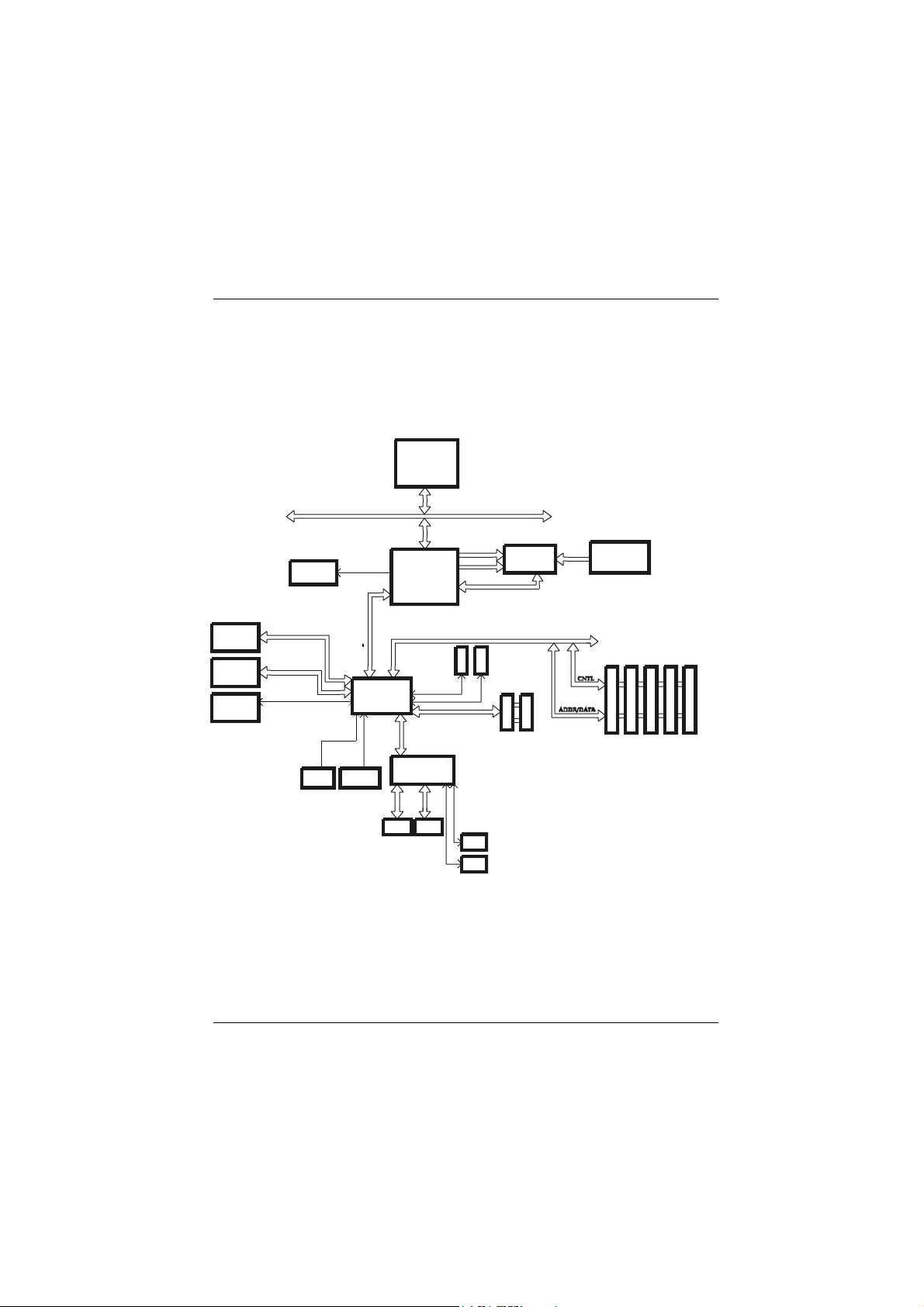
1.2.1 System Block Diagram
AMD K7
PROCESSOR
CNR SLOT
ACR SLOT
AC' 97
CODEC
AGP
MOUSE
HOST BUS
KEYBOARD
V LI NK
VT8233A
VIA
VT8366/A
LPC
WINBOND
W83697HF
FLOPPY
CONN.
FLA SH
BIOS
HOST BUS
CNTL
ADDR
PCI BUS
USB
CNTL
SER.
CONN.
SER.
CONN.
USB
MEM ORY
4 DDR DIMM
DATA
4 USB CONN.
IDE
100/133M HZ
IDE
M7VIB
ATX(F SB: 133/ 10 0MH z)
SUPPORTS 4 DDR DIMMS
SUPPORT 1 A GP SLOT
SUPPORTS 5 PCI S LOTS
SUPPORT 1 ACR SLOT
SUPPORT 1 C NR SLOT
SUPPORT TELEPHON Y
CLOCK
W255
PCI CONN
PCI CONN
PCI CONN
PCI CONN
PCI CONN
1-6
Page 12
Chapter 1 M otherboard Description
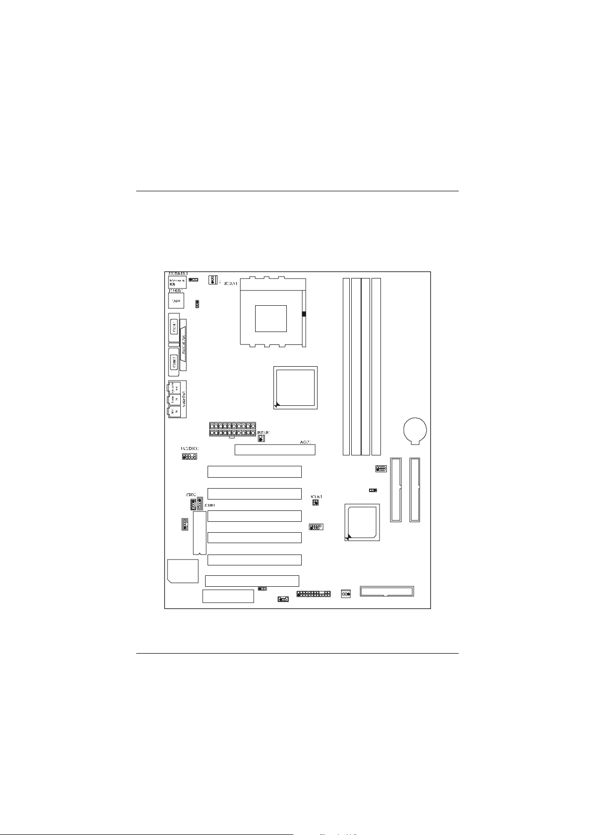
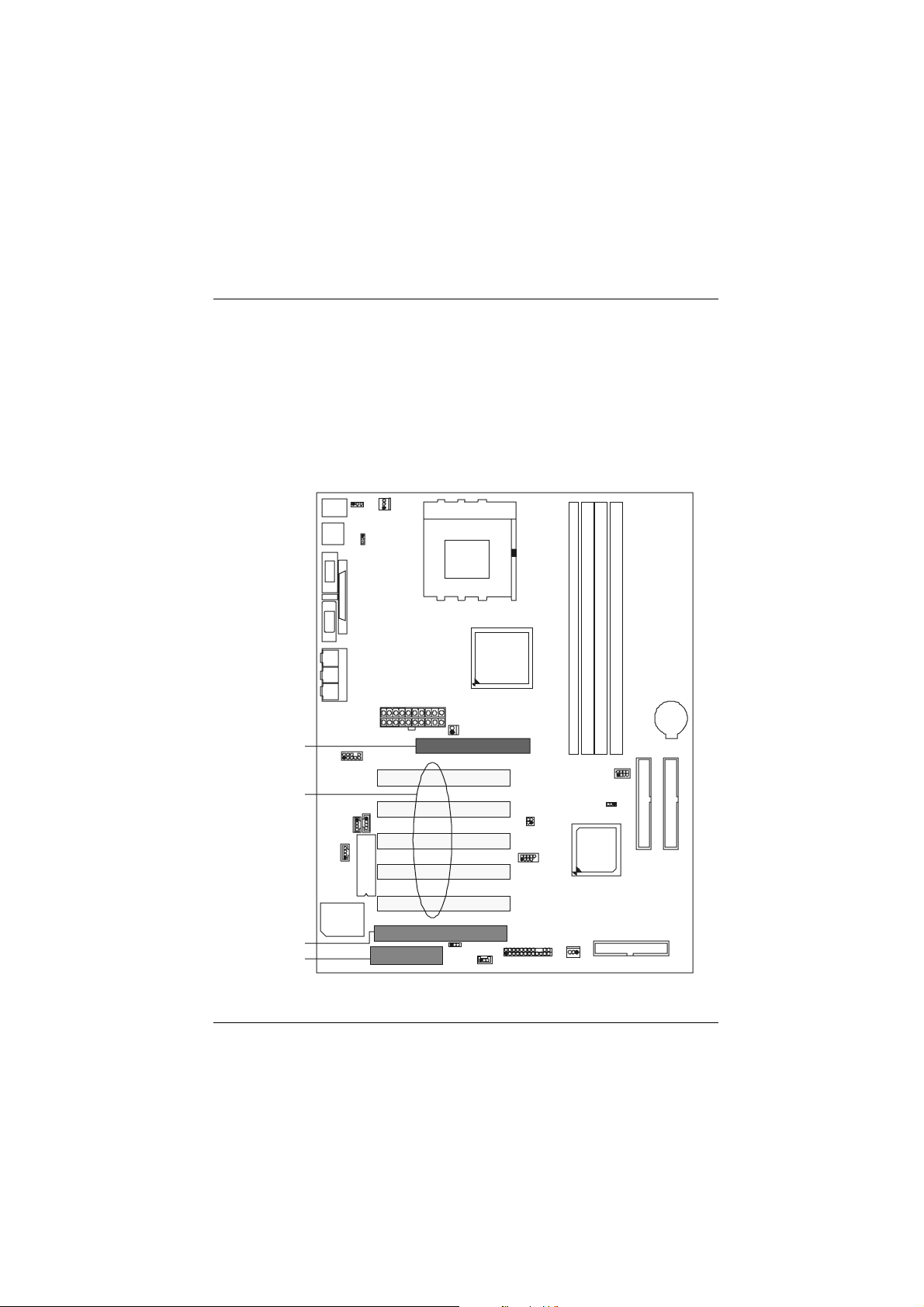
1.2.2 Layout of Motherboard
Model No.M7VIB
JCOM1
1
JKBV1
JUSBV1
Socket A
1
CPU1
CPU
JCOM2
JTAD1
U26
Winbond
W83697
JPRNT1
J8
129
1
1
BIOS
10
1
CNR SLOT
JAT XPWR1
PCI SLOT
PCI SLOT
PCI SLOT
PCI SLOT
PCI SLOT
ACR SLOT
CNR1
1
AG P SLOT
J2
1
VT8366/A
PCI1
PCI2
PCI3
PCI4
PCI5
ACR 1
2
JW OL1
1
1
U2
4
JUS B 2
129
JPANEL1
DIMM1
DIM M3
DIMM2
DIMM4
BAT1
J9
8
127
JCMOS1
VT8233A
FLOPPY D ISK CONN.
1
1
U3
PRIMARY IDE C ONN.
IDE1 IDE2
FDD1
SECONDARY IDE C ONN.
3
12
10
JSFAN1
24
23
1-7
Page 13

Chapter 1 M otherboard Description
1.2.3 Quick Reference
Winbond
W83697
H
I
J
K
L
M
N
BIOS
VT8366/A
VT8233A
DIMM1
DIMM2
DIMM3
DIMM4
ABCDEFG
Y
X
W
V
So ck et A
CPU
U
T
S
OPQ
R
A. Back Panel I/O Connectors O. Clear CMOS (JCMOS1)
B. ATX Power Connector (JATXPWR1) P. DDR DIMM Voltage (J9)
C. AGP Slot (AGP1) Q. IDE Connectors (IDE1-2)
D. Front Audio Header (JAUD IO1) R. D IMMs (DIMM1-4)
E. CD Audio-In Header (JCDIN1) S. CPU Clock Selection (JCLK1)
F. CD Audio-In Head er (JCD IN 2) T. ACR Slo t (ACR1)
G. Telephony Header (JTAD1) U. PCI BUS Slots (PCI1-5)
H. CNR Slot (CNR1) V. North Bridge Chipset (U2) FAN
I. Codec Selection (J2) Header (JNFAN1)
J. Wake-On-LAN Header (JWOL1) W. CPU FAN Head er (JCFAN1 )
K. Front Panel Connector (JPANEL1) X. 5V / 5VSB Selection for USB
L. Front USB Header (JUSB2) (JUSBV1)
M. System FAN Header (JSFAN1) Y. 5V / 5VSB Selection for KB (JKBV1)
N. Floppy Disk Connector (FDD1)
1-8
Page 14
Chapter 1 M otherboard Description
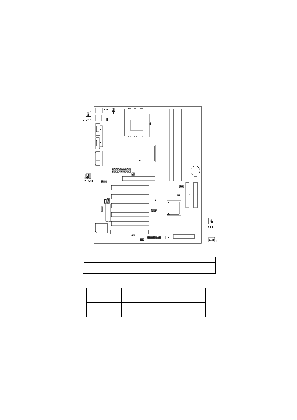
1.3 CPU Installation
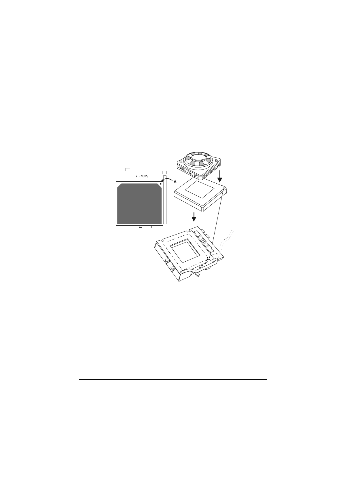
1.3.1 CPU Installation Procedure: Socket A
C
P
U
1. Pull the lever sideways away from the socket then raise the lever up to
90 -degree a ngle.
2. Locate P in A in the socket and look for the white dot or cut edge in the CPU.
Match Pin A with the white dot/cut edge then insert the CPU.
3. Press the lever down.
4. Put the fan on the CP U by buckling it and then put the fan’s powerport into
th e JCF AN1 , then the installatio n will be comp leted.
1-9
Page 15
Chapter 1 M otherboard Description
So cke t A
CPU
VT 8366/ A
DIMM1
DIMM2
DIMM3
DIMM4
BAT1
BIOS
Winbond
W83697
1.3.2 Frequency Selection: JCLK1
CPU Clock PIN 1-2 PIN 3-4
100.0MHz OFF OFF
133.3MHz ON O N
1.3.3 CPU Fan Header: JCFAN1
Pin No. Assignment
1 Ground
2 +12V
3 Sense
1-10
VT8233A
JSFAN1
Page 16

Chapter 1 M otherboard Description
1.3.4 System Fan Header: JSFAN1
Pin No. Assignment
1
2 +12V
3
1.3.5 North Bridge Chipset Fan Header: JNFAN1
Ground
Sense
Pin No. Assignment
1
2 +12V
Ground
1-11
Page 17

Chapter 1 M otherboard Description
1.4 RAM Module Installation
1.4.1 DIMM
DRAM Access Time: 2.5V Unbuffered/ Registered DDR SDRAM PC1600/
DRAM Type : 64MB/ 128MB/ 256MB/ 512MB/ 1GB DIMM Module (184 pin)
Devices used on
DIMM
64M (4Mx4x4banks) 256 M 256 M 256 M 256 M
64M (2Mx8x4banks) 128 M 128 M 128 M 128 M
64M (1Mx16x4banks) 64 M 64 M 64 M 64 M
128M (8Mx4x4banks 512 M 512 M 512 M 512 M
128M (4Mx8x4banks) 256 M 256 M 256 M 256 M
128M (2Mx16x4banks) 128 M 128 M 128 M 128 M
256M (16Mx4x4banks) 1 G 1 G 1 G 1 G
256M (8Mx8x4banks) 512 M 512 M 512 M 512 M
256M (4Mx16x4banks) 256 M 256 M 256 M 256 M
512M (16Mx8x4banks) 1 G 1 G 1 G 1 G
512M (8Mx16x4banks) 512 M 512 M 512 M 512 M
* This M7VIB motherboard does not support with parity DIMM.
*The list shown above for DRAM configuratio n is onl y for reference.
PC2100 Type required.
Total Memory Size
DIMM 1
(2 Rows)
x64
DIMM 2
(2 Rows)
x64
DIMM 3
(2 Rows)
x64
DIMM 4
(2 Rows)
x64
1-12
Page 18
Chapter 1 M otherboard Description
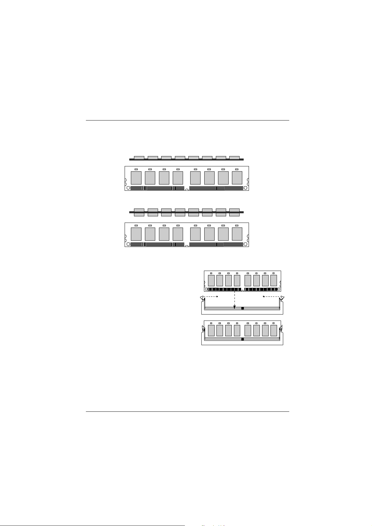
1.4.2 How to install a DIMM Module
1. The DIMM socket has a “ Plastic Safety
Tab”, and the DIMM memory module has
an “Asymmetrical notch”, so the DIMM
memory module can only fit into the slot
in one direction.
2. Push the tabs out. Insert the DIMM
memory modules into the socket at a
90-degree angle, and then push down
ver tica lly so that it will f it int o the place .
3. The Mounting Holes and plast ic tabs
should fit over the edge and hold the
DIMM memory modules in place.
Single Sided DIMM
Double Sid ed DIMM
1-13
Page 19
Chapter 1 M otherboard Description
1.5 Slots
The slots in this motherboard are designed to hold expans ion cards and connect them to
the system bus. Expansion slots are a mean of adding or enhancing the motherboard's
features and capabilities. With these efficient facilit ies, you can increase the
motherboard's capabilit ies by adding hardware that performs tasks that are not part of
the basic system.
Socket A
CPU
DIMM1
DI MM2
DIMM3
DI MM4
VT8366/ A
AGP SLOT
PCI SLOT
ACR SLO T
CNR SLOT
Winbon d
W836 97
BIOS
VT82 33A
1-14
Page 20

Chapter 1 M otherboard Description
1.5.1 ACR (Advanced Communication Riser) Slot
The ACR specif ication is an open Industry Standard Architecture, and it def ines a
hardware scalable riser card interface, which supports audio and modem only.
1.5.2 AGP (Accelerated Graphics Port) Slot
Unlike the mouse ports, keyboard ports and printer ports, this motherboard does not
have built in video facilities; and therefore, requires a video card for one of the
expansion slots. Your monitor will attach directly to that video card. This
motherboard supports video cards for PCI and ISA slots, but it is also equipped
with an Accelerated Graphics Port (AGP). An AGP card will take advantage of
AGP technology for improved video efficiency and performance, especially with
3D gra phics.
1.5.3 CNR (Communication Network Riser) Slot
The CNR specification is an open Industry Standard Architecture, and it def ines a
hardware scalable riser card interface, which supports audio and modem only.
1.5.4 PCI (Peripheral Component Interconnect) Slots
This motherboard is equipped with 5 standard PCI slots. PCI stands for Peripheral
Component Interconnect, and it is a bus standard for expansion cards, which has
supplanted the older ISA bus standard in most parts. This PCI slot is designated as
32 b its.
1-15
Page 21
Chapter 1 M otherboard Description
1.6 Connectors, Headers & Jumpers
The connectors, headers and jumpers introduced below provide you lots of
capabilities such as power supply, front panel signal revelation, IDE hard disk
connection, floppy disk connection, Wake On LAN function and USB connection.
Noticeably, a jumper has two or more pins that can be covered by a plastic jumper
cap, allowing you to select a different system options.
JKBV1
1
JUSBV1
1
Socket A
CPU
VT8366/A
DIMM1
DIMM2
DIMM3
DIMM4
JATXPWR1
Winbond
W83697
BIOS
J9
8
127
IDE1-2
VT8233A
JCMOS1
1
JUSB2
2
10
9
1
J2
1
JWO L1
1
JPANEL1
FDD1
1-16
Page 22
Chapter 1 M otherboard Description
N
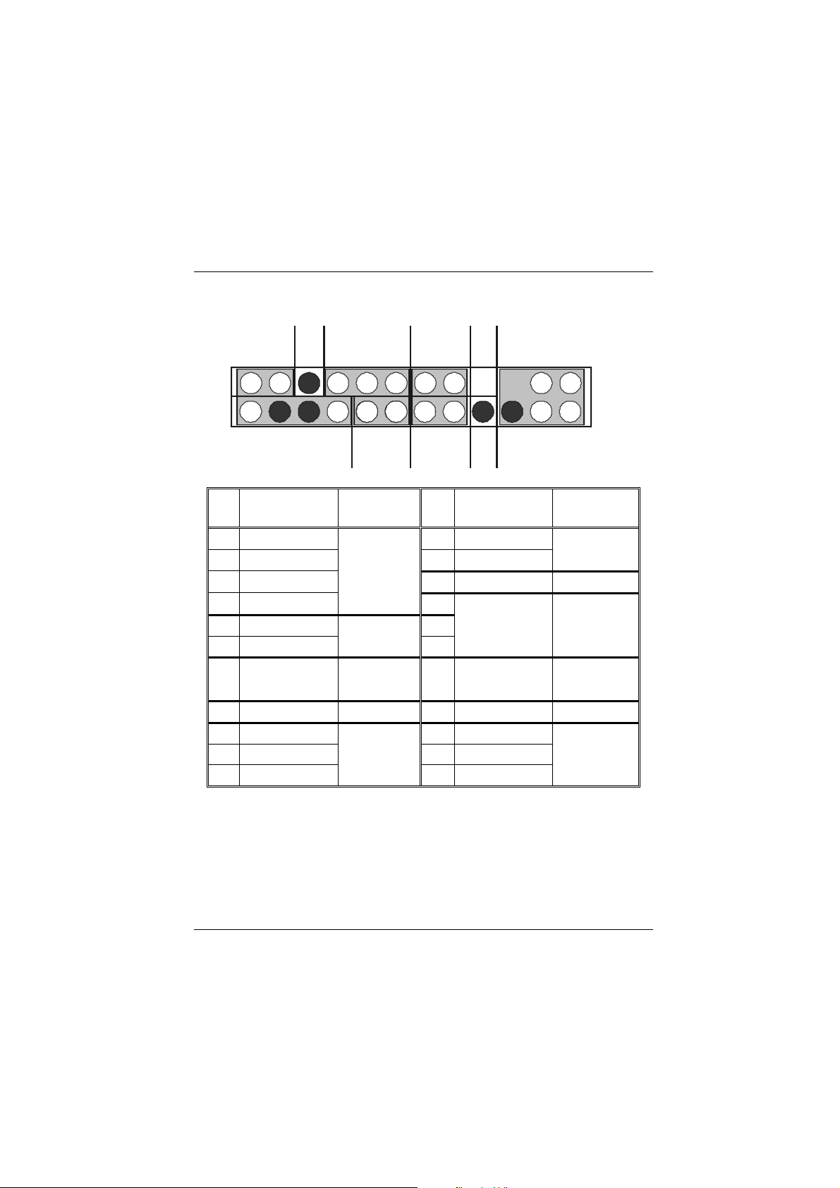
1.6.1 Front Panel Connector: JPANEL1
24
23
SLP
NA
POW-LED
(-)(+) (+)
ON/OFF
K
E
Y
IR
2
1
SPK
Pin Assignment Function Pin Assignment Function
No.
1
3
5
7
9
11
13
15
17
19
21
23
+5V 2 Sleep Control Sleep
NA Speaker 4 Ground Button
NA Connector
Speaker 8 Power LED (+)
HDD LED (+) Hard Drive
HDD LED (-) LED
Ground Reset
Reset Control Button
NA
NA IrDA
VCC5 Connector
IRT X
SPK (Speaker Connector)
An offboard speaker can be installed on the motherboard as a manufacturing option.
It can be connected to the motherboard at the front panel connector. The speaker
(onboard or offboard) provides error beep code information during the Power On
Self-Test when the computer cannot use the video interface. The speaker is not
connected to the audio subsystem and does not receive output from the audio
subsystem.
HLED
(-)(+)
ARST
No.
6
10
12
14
16
18
20
22
24
NA NA
Power LED (+) POWER
Power LED (-) LED
Power Button Power-on
Ground Button
KEY
KEY IrDA
Ground Connector
IRRX
1-17
Page 23

Chapter 1 M otherboard Description
RST (Reset Button)
This connector can be attached to a momentary SPST switch. This switch is usually
open, and when it is closed, it will cause the motherboard to reset and run the POST
(P ower O n S elf Te st).
POW-LED (Power LED Connector)
This connector can be attached to an LED on the front panel of a computer case.
The LED will illuminate while the computer is powered on.
HLED (Hard Drive LED Connector)
This connector can be attached to an LED on the front panel of a computer case.
Th e LE D will flicker d ur in g disk ac t ivity wh ere it is on ly applied to those IDE
drives directly attached to the system board.
IR (Infrare d Connecto r)
This connector is used to attach to an infrared sensing device. After the IrDA
interface is configured, connectionless data transfer to and from portable devices
suc h as la ptops m aking PD As is poss ib le.
SLP (S lee p/Green Button)
This connector is used to conserve energy by powering down the monitor and the
hard disk when is not in use. To configure this option, you need to connect a button
from the front panel to this sleep button. Depressing the button will power down
the monitor and t he hard driv es un til the system is invoked by any keyboard activity,
mouse activity, modem activity or when the sleep button is depressed again. APM
(Advanced Power Management) must be enab led in the system BIOS and the APM
driver must be loaded.
ON/ OF F (Powe r B utto n)
This connector can be attached to a front panel power switch. The switch must
pulled the Power Button pin to ground for at least 50 ms to signal the power supply
to switch on or off. (T he time required is due to internal debounce circu itry on the
system board). At least two seconds must pass before the power supply will
recognize another on/off signal.
1-18
Page 24

Chapter 1 M otherboard Description
1.6.2 ATX 20-pin Power Connector: JATXPWR1
This connector supports the power button on-board. Using the ATX power supply,
function such as Soft Power Off, is supported on this motherboard. This power
connector supports instant power-on functionality, which means that the system
will boot up instantly when the power connector is inserted on the board.
PIN Assignment PIN Assignment
1 3.3V 11 3.3V
2 3.3V 12 -12V
3 Ground 13 Ground
4 5V 14 PS _ON
5 Ground 15 Ground
6 5V 16 Ground
7 Ground 17 Ground
8 PW_OK 18 -5V
9 5V_SB 19 5V
10 12V 20 5V
1.6.3 H ard Disk Connectors: IDE1/IDE2
The motherboard has a 32-bit Enhanced PCI IDE Controller that provides PIO
Mode 0~4, Bus Master, and Ultra DMA 33, Ultra DMA 66,Ultra DMA 100, Ultra
DMA 133 functiona lity. It has two HDD connectors: IDE1 (primary) and IDE2
(secondary). You can connect up to four hard disk drives, a CD-ROM, a 120MB
Floppy (reserved for future BIOS) and other devices to IDE1 and IDE2. T hese
connectors support the IDE hard disk cable provided.
• IDE1 (Primary IDE Connector)
The first hard drive should always be connected to IDE1. IDE1 can connect a
Master and a Slave drive. You must configure the second hard drive on IDE1 to
Slave mode by setting the jumper accordingly.
• IDE2 (Secondary IDE Connector)
The IDE2 controller can also support a Master and a Slave drive. Its configuration
is similar to IDE1. The second drive on this controller must be set to slave mode.
1-19
Page 25

Chapter 1 M otherboard Description
1.6.4 Floppy Disk Connector: FDD1
The motherboard provides a standard floppy d isk connector (FDC) that supports
360K, 720K, 1.2M, 1.44M and 2.88M floppy disk types. This connector supports
the provided floppy drive ribbon cables.
1.6.5 Wake On LAN Header: JWOL1
Pin No. Assignment
1
2 Ground
3
5V SB
Wake up
1.6.6 Clear CMOS Jumper: JCMOS1
JCMOS1 Assignment
1 3
1-2 Closed
1 3
2-3 Closed
Normal Operation (default)
Clear CMOS Data
Remove AC
power line
AC po we r o n
The follo wing proced ures are for res etting
the BIOS password. It is important to
follo w these instructions closely.
JCMOS1
(2-3) closed
Wait five
seconds
JCMOS1
(1-2) closed
Reset your desired password
or clear CMOS data
1-20
Page 26

Chapter 1 M otherboard Description
1.6.7 Front USB Header: JUSB2
Note:
Before you install this header, make sure the pin assignments
are corresponded to the table below; otherwise, it may cause great
damage to your USB device.
(JU SB2)
Pin Assignment Pin Assignment
1 +5V(fused) 2 +5V(fused)
3 USBP2- 4 USBP3-
5 USBP2+ 6 USBP3+
7 Ground 8 Ground
9 KEY 10 NC
1.6.8 CNR Codec Primary/Secondary Selection: J2
Pin No. Assignment
1-2
2-3 CNR Primary Codec
On-board Primary Codec
1.6.9 DDR DIMM Voltage: J9
Pin DDR DIMM Voltage
1-2
3-4 2.65V (Default)
5-6
7-8
z If you meet the DDR DIMM compatible program, try to adjust the DDR Voltage to
fix the compatible program.
2.55V
2.75V
2.85V
1-21
Page 27

Chapter 1 M otherboard Description
1.6.10 5V/ 5VSB Selection for USB: JUSBV1
JUSBV1 Assignment
1 3
1-2 Closed
1 3
2-3 Closed
5V
5V_SB
1.6.11 5V/ 5VSB Selection for KB: JKBV1
JKBV1 Assignment
1 3
1-2 Closed
1 3
2-3 Closed
5V
5V_SB
1-22
Page 28

Chapter 1 M otherboard Description
1.7 Peripheral Port
JKBMS1
PS/2
Mouse
JUSB1
JPRNT1
Parallel
J8
Game Port
PS/2
Key board
USB
COM1
COM2
Speaker
Out
Line In Mic
JCOM2JCOM1
1.7.1 PS/2 Mouse / Keyboard Conn ect or : JKBM S1
The motherboard provides a standard PS/2 mouse / Keyboard mini DIN connector
for attaching a PS/2 mouse. You can plug a P S/2 mouse / Keyboard directly into
this connector. The connector location and pin definition are shown below:
In
1-23
Page 29

Chapter 1 M otherboard Description
PS/2 Mouse / Keyboard Connectors
Pin Assig nment
1 Data
2 No connect
3 Ground
4 +5 V (fused)
5 Clock
6 No connect
1.7.2 USB Connector: JUSB1
The motherboard provides a OHCI (Open Ho st Co ntro ller Inte rface) Unive rsal
Serial Bus Roots for attaching USB devices such as: keyboard, mouse and other
USB devices. You can plug the USB devices directly into this connector.
Stacked USB Connectors
Pin Assig nment
1 +5 V (fused)
2
3
4 Ground
Signal names in brackets ([]) are for USB Port 1.
USBP0- [USBP1-]
USBP0+ [USBP1+]
1-24
Page 30

Chapter 1 M otherboard Description
1.7.3 Serial and Parallel Interface Ports
This system is equipped with two serial ports and one paralle l port. Both types of
interface ports will be explained in this chapter.
1.7.3.1 Th e S er ia l In terface : JCOM1/ J COM2
The serial interface port is sometimes referred to as an RS-232 port or an
asynchronous communication port. Mice, printers, modems and other peripheral
devices can be connected to a serial port, where it can also be used to connect your
computer with another computer system. If you wish to transfer the contents of
your hard disk to another system, it can be accomplished by using each machine’s
seria l port.
The serial port on this system has two 9-pin connectors. Some older computer
systems and peripherals used to be equipped with on ly one 25-pin connector. If you
need to connect a 9-pin serial port to an older 25-pin ser ial port, you can purchase a
9-to-25 pin adapter.
1-25
Page 31

Chapter 1 M otherboard Description
Connectivity
The serial ports can be used in many ways, and it may be necessary to become
familiar with the pinout diagram. The following chart gives you the function of
each pin on the 9-pin connector and some of the 25-pin connector. This information
can be used when configur ing certain software programs to work with the serial
ports .
Signal Name DB9 PIN DB25 PIN
DCD Data Carrier Detect 1 8
RX Receive Data 2 3
TX Transmit Data 3 2
DTR Data Terminal Ready 4 20
GND Signal Ground 5 7
DSR Data Set Ready 6 6
RTS Request to Send 7 4
CTS Clear to Send 8 5
RI Ring Indicator 9 22
1-26
Page 32

Chapter 1 M otherboard Description
1.7.3.2 Parallel Interface Port: JPRNT1
Unlike the serial ports, parallel interface port has been standardized, and it should
not present any difficulty interfacing peripherals of your system. Sometimes called
centronics port, the parallel port is almost exclusively used with printers. The
parallel port on your system has a 25-pin, DB25 connector (see picture below). The
pinout for the parallel port are shown in the table below.
Signal Pin
-Strobe 1
Data 0 2
Data 1 3
Data 2 4
Data 3 5
Data 4 6
Data 5 7
Data 6 8
Data 7 9
-Ack 10
Busy 11
Paper Empty 12
+Select 13
-Auto FDXT 14
-Error 15
-Init 16
-SLCTN 17
Ground 18
Ground 19
Ground 20
Ground 21
Ground 22
Ground 23
Ground 24
Ground 25
1-27
Page 33

Chapter 1 M otherboard Description
1.7.4 Game (Jo ystick/MID I) Port Conn ect or: J8
This connector allows you to connect a joystick or game pad for playing computer
games. Also, you may play or edit professional music by connecting MIDI devices.
Game/Joystick/MIDI
1.7.5 Audio Port Connectors: J8
Spe aker Out is used to connect speakers or headphones for audio output.
Line In can be connected to the external CD player, Tape player or other audio
dev ices for a udio input .
Mic In is used to connect a microphone that allows you to input sounds and voices.
Speake r Out Line In Mic In
1-28
Page 34

Chapter 1 M otherboard Description
1.7.6 Audio Subsystem
10
2
1
9
1
Socket A
CPU
DIMM1
DIMM2
DIMM3
DIMM4
VT8366/A
1
VT8233A
BIOS
1
Winbond
W83697
1-29
Page 35

Chapter 1 M otherboard Description
1.7.6.1 CD-ROM Audio-In Header: JCDIN1
Pin No. Assignment
1 Left Channel Input
2 Ground
3 Ground
4 Right Channel Input
1.7.6.2 CD-ROM Audio-In Header: JCDIN2
Pin No. Assignment
1 Left Channel Input
2 Ground
3 Right Channel Input
4 Ground
1.7.6.3 Front Panel Audio Header: JAUDIO1
Pin No. Assignment Pin No. Assignment
1 Mic In 2 Ground
3 Mic Power 4 Audio Power
5 RT Line Out 6 RT Line Out
7 Reserved 8 Key
9 LFT Line Out 10 LFT Line Out
1.7.6.4 Telephony Audio Header: JTAD1
Pin No. Assignment
1 MONO_IN
2 Ground
3 Ground
4 MONO_OU T
1-30
Page 36

Chapter 2 BIOS Setup
2. BIOS Setup
Introduction
This manual discussed Award™ Setup program built into the ROM BIOS. The
Setup program allows users to modify the bas ic system configurat ion. This special
information is then stored in battery-backed RAM so that it retains the Setup
information when the power is turned off.
The Award BIOS™ installed in your computer system’s ROM (Read Only Memory)
is a custom version of an industry standard BIOS. This means that it supports
AMD-Athlon
critical low-level support for standard devices such as disk drives and serial/
parallel ports.
Add ing important has customized the Award BIOS™, but nonstandard features
such as virus and password protection as well as special support for detailed
fine -tun in g of the c hipse t con trols the entire system.
The rest of this manual is intended to guide you through the process of configuring
your system by using Setup.
Plug a nd Play Support
These AWARD BIOS supports the Plug and Play Version 1.0A specification.
ESCD (Extended System Configuration Data) write is supported.
EPA Green PC Support
This AWARD BIOS supports Version 1.03 of the EP A Green PC specification.
APM Support
These AWARD BIOS supports Version 1.1&1.2 of the Advanced P ower
Management ( APM) specification. Power management features are implemented
via the System Management Interrupt (SMI). Sleep and Suspend power
management modes are supported. This AWARD BIOS can manage power to the
hard dis k drives a nd video m onitors.
TM
/ Duron
TM
processors input/output system. The BIOS provides
2-1
Page 37

Chapter 2 BIOS Setup
PCI Bus Suppo rt
This AWARD BIOS also supports Version 2.1 of the Intel P CI (Peripheral
Component Interconnect) local bus specification.
DRAM Support
DDR SDRAM (Double Data Rate Synchronous DRAM) is supported.
Suppo rted CP Us
Th is AW AR D BI O S s u p port s the AM D Ath lonTM / Duron
TM
/ Athlon XP
TM
CPU.
Us i ng Se t up
In general, you use the arrow keys to highlight items, press <Enter> to select, use
the <PgU p> and <PgDn> keys to ch ange entr ies, p ress <F1> for help and pres s
<Esc> to quit. The following table provides more detail about how to navigate in
the Setup program by using the keyboard.
Keystroke Function
Up arrow Move to p revio us item
Down arrow Move to next item
Left arro w Move to t he item o n the left (menu bar)
Right arrow Move to the item on the right (men u bar)
Esc Mai n Men u: Quit wit hout saving c hanges
Move Enter Move to the item yo u desired
PgUp key Increase the numeric value or make changes
PgDn key Decrease the numeric value or make changes
+ Key Increase the numeric value or make changes
- Key Decrease the numeric value or make changes
Esc key Main Me nu – Quit and not save changes into CMOS
F1 key Genera l help on Setup navigation keys
F5 key Load previous values from CMOS
F6 key Load the fail-safe defaults from BIOS default table
F7 key Load the optimized defaults
F10 key Save all the CMOS changes a nd exit
Submenus: Exit Current page to the next hig her level menu
Status Page Setup Menu and Option Page Setup Menu – Exit
Current page and return to Main Menu
2-2
Page 38

Chapter 2 BIOS Setup
2.1 Main Menu
Once you enter Award BIOS™ CMOS Setup Utility, the Main Menu will appear on
the screen. The Main Menu allows you to select from several setup functions. Use
the arrow keys to select among the items and press <Enter> to accept and enter the
sub-menu.
!! WARNING !!
The information about BIOS defaults on manual (Figure
1,2,3,4,5,6,7,8) is just for reference; please refer to the BIOS
installed on board, for update information.
Figure 1. Main Menu
Sta nda rd CMOS Feat ures
This submenu contains industry standard configurable options.
Advance d BIOS Features
This submenu allows you to configure enhanced features of the BIOS.
2-3
Page 39

Chapter 2 BIOS Setup
Advanced Chipset Features
This submenu allows you to configure special chipset features.
In teg ra ted Pe riphe rals
This submenu allows you to configure certa in IDE hard drive options and
Programmed Input/ Output features.
Power Management Setup
This submenu allows you to configure the power management features.
PnP/PCI Configura tions
This submenu allows you to configure certain “P lug and P lay” and PCI options.
PC Health Status
This submenu allows you to monitor the hardware of your system.
Frequenc y/Voltage Control
This submenu allows you to change CP U Vcore Voltage and CPU/PCI clock.
(Ho weve r, thi s fu nctio n is stro ng ly recom m ended no t to use. Not pro perly
change the voltage and clo ck may cause CPU or M/B damage!)
Load Optimized Defaults
This selection allows you to reload the BIOS when the system is having problems
particularly with the boot sequence. These configurat ions are factory settings
optimized for this system. A confirmation message will be displayed before
default s are se t.
Set Supervisor Password
Setting the supervisor password will prohibit everyone except the supervisor from
making changes using the CMOS Setup Utility. You will be prompted with to
enter a p assw ord.
2-4
Page 40

Chapter 2 BIOS Setup
Set User Password
If t he Supervisor Pass word is not set, then the User Pass word will funct ion in t he
same way as the Supervisor Password. If the Supervisor Password is set and the
User Password is set, the “User” will only be able to view configurations but will
not be able to change them.
Save & Exit Setup
Save all conf iguration changes to CMOS(memory) and exit setup. Confirmation
message will be displayed before proceeding.
Exit Without Saving
Abandon all changes made during the current session and exit setup.
Confirmation message w ill be displayed before proceedin g.
Update BIOS
This submenu allows you to update bios.
2-5
Page 41

Chapter 2 BIOS Setup
2.2 Standard CMOS Features
The items in Standard CMOS Setup Menu are divided into 10 categories. Each
category includes no, one or more than one setup items. Use the arrow keys to
high l ight the item and then u se the<P gUp> or <P gDn> k eys to selec t the valu e you
want in each item.
Figure 2. Standard CMOS Setup
2-6
Page 42

Chapter 2 BIOS Setup
Main Menu Selec tions
This table shows the selections that you can make on the Main Menu.
Item Options Description
Date MM DD YYYY Set the system date. Note
that the ‘Day’ automatically
changes when you set the
date.
Time HH MM SS Set the system internal
clock.
IDE Primary Master Options are in its sub
menu.
IDE Primary Slave Options are in its sub
menu.
IDE Secondary Master Options are in its sub
menu.
IDE Secondary Slave Options are in its sub
menu.
Drive A
Drive B
360K, 5.25 in
1.2M, 5.25 in
720K, 3.5 in
1.44M, 3.5 in
2.88M, 3.5 in
None
Video EGA/ VG A
CGA 40
CGA 80
MONO
Press <Enter> to enter the
sub menu of detailed
optio ns
Press <Enter> to enter the
sub menu of detailed
optio ns.
Press <Enter> to enter the
sub menu of detailed
optio ns.
Press <Enter> to enter the
sub menu of detailed
optio ns.
Select the type of floppy
disk drive installed in your
system.
Select the default video
device .
2-7
Page 43

Chapter 2 BIOS Setup
Item Options Description
Halt On All Errors
No Errors
All, but Keyboard
All, but Diskette
All, but Disk/ Key
Base Memory N/A Displays the amount of
Extended Memory N/A Displays the amount of
Total Memory N/A Displays the total me mory
Select the situation in which
you want the BIOS to stop
the POST process and
notify you.
conventional memory
detected during boot up.
extended me mory detected
during boot up.
available in the system.
2-8
Page 44

Chapter 2 BIOS Setup
2.3 Advanced BIOS Features
Fig ure 3. Adva nce d BIOS Se tup
Virus Warning
This option allows you to choose the VIRUS Warning feature that is used to protect
the IDE Hard Disk boot sector. If this function is enabled and an attempt is made to
writ e to t he boot sector, BI OS w ill d isplay a warn in g messa ge on the s cree n and
sound an alarm beep.
CPU Internal Cache
Depending on the CPU/chipset in use, you may be able to increase memory access
time with th is opt ion.
Disabled (default) Virus protection is disabled.
Enabled Virus protection is activated.
Enabled (default) Enable cache.
Disabled Disable cache.
2-9
Page 45

Chapter 2 BIOS Setup
Extermal Cache
This option enables or disables “Level 2” secondary cache on the CP U, which may
improve performance.
Enabled (default) Enable cache.
Disabled Disable cache.
CPU L2 Cache ECC Checking
Th is item al lows y ou to en able/ disab le CP U L2 Cac he ECC Che cking.
The Choices: Enabled (default), Disabled.
Quick Power On Self Test
Ena blin g th is opt ion wi ll cause an ab ridged ve rsion of the P ow er On Self-Te st
(POST ) to execute after you power up the computer.
Enabled (default) Enable quick POST.
Disabled Normal POST.
First /Seco nd/Third/ Boot Othe r De vice
These BIOS attempts to load the operating system from the devices in the sequence
selected in these items.
The Choices: Floppy, LS120, HDD-0, SCSI, CDROM, HDD-1, HDD-2,
HDD-3, ZIP100, LAN, Disabled, Enabled.
Swap Floppy Drive
For systems with two floppy drives, this option allows you to swap logica l drive
assignments.
The Choices: Enabled, Disabled (default).
Boot Up Floppy Seek
Enabling this option will test the floppy drives to determine if they have 40 or 80
tracks. Disabling this option reduces the time it takes to boot-up.
The Choices: En a bl ed (default), Disabled.
2-10
Page 46

Chapter 2 BIOS Setup
Boot Up NumLock Status
Selects the NumLock. State after power on.
On (default) Numpad is number keys.
Off Numpad is arrow keys.
Gate A20 Option
Select if chipset or keyboard controller should control Gate A20.
Normal A pin in the keyboard controller
controls Gate A20.
Fast (d efau lt) Let s chipset co ntro l Gate A20 .
Typematic Rate Setting
When a key is held down, the keystroke will repeat at a rate determined by the
keyboard controller. When enabled, the typematic rate and typematic delay can be
configured.
Disabled (default)
Enabled
Typematic Rate (Chars/Sec)
Sets the rate at which a keystroke is repeated when you hold the key down.
The Choices: 6 (default), 8,10,12,15,20,24,30.
Typematic Delay (Msec)
Sets the delay time after the key is held down before it begins to repeat the
keystroke.
The Choices: 250 (default), 500,750,1000.
Securi ty Optio n
Th is option will e nable on ly ind iv idua ls w it h passw ords to br ing the sy stem onlin e
and /or t o use the CMOS Setup Utilit y.
System A password is required for the system to
boot and is also required to access the Setup
Utility.
Setup (default) A password is required to access the Setup
Utility only.
This will only app ly if passwords are set from the Setup main menu.
2-11
Page 47

Chapter 2 BIOS Setup
APIC Mode
Selecting Enabled enables AP IC device mode reporting from the BIOS to the
ope ratin g sy stem.
The Choices: En abled, Di sable d (default).
MPS Vers ion Co ntrol Fo r OS
The BIOS supports versions 1.1 and 1.4 of the Intel multiprocessor specif ication.
Select the version supported by the operation system running on this computer.
The Choices: 1.4 (default), 1.1.
OS Select For DRAM > 64MB
A choice other than Non-OS2 is only used for OS2 systems with memory
exceeding 64MB.
The Choices: No n-OS2 (default), OS2.
Video BIOS Shadow
Determines whether video BIOS will be copied to RAM for faster execution.
Enabled (default) Optional ROM is enabled.
Disabled Optional ROM is disabled.
2-12
Page 48

Chapter 2 BIOS Setup
2.4 Advanced Chipset Features
This submenu allows you to configure the specific features of the chipset installed on
your system. This chipset manages bus speeds and access to system memory resources,
such as DRAM and external cache. It also coordinates communications with the PCI
bus. The default settings that came with your system have been optimized and therefore
should not be changed unless you are suspicious that the settings have been changed
incorrect ly.
Fig ure 4. Adva nce d Chi pse t Setup
DRAM Clock/Drive Control
To control the Clock/Drive. If you highlight the litera l “Press Enter” next to the
“DRAM Clock/Drive Control” label and then press the enter key, it will take you a
submenu with the follow ing options:
DRAM Clo ck
This item determines DRAM clock following 100MHz, 133MHz or By
SPD.
The Choices: 100MHz, 133MHz, By SPD (default).
2-13
Page 49

Chapter 2 BIOS Setup
DRAM Timing
This item determines DRAM clock/ timing follow SPD or not.
The Choices: By SPD (default), Manual.
SDRAM Cycle Length
When synchronous DRAM is installed, the number of clock cycles of
CAS latency depends on the DRAM timing. Do not reset this field from
the default value specified by the system designer.
The Choices: 3(default), 2.5, 2.
Bank Interleave
This item allows you to enable or disable the bank interleave feature.
The Choices: Disabled (default), 2 b ank, 4 ba nk.
DRAM Queue Depth
This item permits to place the depths of the memory. The deeper the
depth is, the better is this function.
The Choices: 4 level (defa ult), 2 level, 3 leve l.
DRAM Command Rate
This item controls c lock cycle that must occur between the last valid
write operation and the next command.
The Choices: 1T Command, 2T Command (default).
AGP & P2P Bridge Co ntrol
If you highlight the literal “Press Enter” next to the “AGP & P2P Bridge Control”
label and then press the enter key, it will take you a submenu with the following
options :
AGP Ap erture S ize
Select the s ize of the Accelerated Graphics Port (AGP) aperture. T he
aperture is a portion of the PCI memory address range dedicated for
graphics memory address space. Host cycles that hit the aperture range
are forwarded to the AGP without any translation.
The Choices: 64M (default), 256M, 128M, 32M, 16M, 8M, 4M.
AGP Mode
This item allows you to select the AGP Mode.
The Choices: 4X (default), 2X, 1X.
2-14
Page 50

Chapter 2 BIOS Setup
AGP Driving Co ntro l
By choosing “Auto” the system BIOS will the AGP output Buffer Drive
strength P Ctrl by AGP Card. By choosing “Manual”, it allows user to set
AGP output Buffer Drive strength P Ctrl by manual.
The Choices: Auto (default), Manual.
AGP Driving Value
While AGP driving control item set to “Manual”, it allows user to set
AGP d rivin g.
The Choices: DA (default).
AG P Fast Write
The Choices: Enabled, Disabled (default).
AGP Master 1 WS Write
When Enabled, writes to the AGP (Accelerated Graphics Port) are
executed with one-wait states.
The Choices: Disabled (default), Enabled.
AGP Master 1 WS Read
When Enabled, read to the AGP (Accelerated Graphics Port) are
executed with one wait states.
The Choices: Disabled (default), Enabled.
CPU & PCI Bus Control
If you highlight the literal “P ress Enter” next to the “CPU & PCI Bus Control” labe l
and then press the enter key, it will take you a submenu with the following options:
PCI1 Master 0 WS Write
When enabled, writes to the PCI bus are executed with zero-wait states.
The Choices: Enabled (default), Disabled.
PCI2 Master 0 WS Write
When enabled, writes to the AGP bus are executed with zero-wait states.
The Choices: Enabled (default), Disabled.
PCI1 Po st Write
Wh en En abled, CP U w rites are allowe d to post on the P CI bus.
The Choices: Enabled (default), Disabled.
2-15
Page 51

Chapter 2 BIOS Setup
PCI2 Po st Write
Wh en En abled, CP U w rites are allowed to post on the AGP bus.
The Choices: Enabled (default), Disabled.
PCI Delay Transaction
The chipset has an embedded 32-bit posted write buffer to support delay
transactions cycles. Select Enabled to support compliance with PCI
specification.
The Choices: Enabled (default), Disa bled.
Memory Hole
When enabled, you can reserve an area of system memory for ISA adapter ROM.
When this area is reserved, it cannot be cached. Refer to the user documentation of
the peripheral you are installing for more information.
The Choices: Disabled (de fault), 15M – 16M.
System BIOS Cacheable
Selecting the “Enabled” option allows caching of the system BIOS ROM at
F0000h-FFFFFh, which can improve system performance. However, any programs
writ ing to this area of memory will cause conflicts and result in system errors.
The Ch o i ces : Enabled, Disabled (default).
Video RAM Cacheable
Ena blin g th is opt ion a llows c achin g of the video R AM, r esult ing in be tter syst em
performance. However, if any program writes to th is memory area, a system error
may result.
The Cho ices: En abled, Disabled (default).
2-16
Page 52

Chapter 2 BIOS Setup
2.5 Integrated Peripherals
Figure 5. Integrated Peripherals
VIA OnChip IDE Device
If you highlight the literal “Press Enter” next to the “VIA O n C h i p I D E D e v ic e”
label and then press the enter key, it will take you a submenu with the following
options :
OnChip IDE Ch ann el 0/1
The motherboard chipset contains a PCI IDE interface with support for
two IDE channels. Select “Enabled” to activate the first and/or second
IDE interface. Select “Disabled” to deactivate an interface if you are
going to install a primary and/or secondary add-in IDE interface.
The Choices: Enabled (default), Disabled.
IDE Prefetch Mode
The “onboard” IDE drive interfaces supports IDE prefetching for faster
drive access. If the interface does not support prefetchin g. If you install
a primary and/or secondary add-in IDE interface, set this option to
“D isab led”.
The Choices: Enabled (default), Disabled.
2-17
Page 53

Chapter 2 BIOS Setup
Primary / Secondary /Master / Slave PIO
The IDE PIO (Programmed Input / Output) fields let you set a PIO
mode (0-5) for each of the IDE devices that the onboard IDE interface
supports. Modes 0 to 5 will increase performance progressively. In Auto
mode, the system automatically determines the best mode for each
device.
The Choices: Auto (default), Mode0, Mode1, Mode2, Mode3, Mode4,
Mode5.
Primary / Secondary /Master / Slave UDMA
Ultra DMA/133 functionality can be implemented if it is supported by
the IDE hard drives in your system. As well, your operating environment
requires a DMA driver (Windows 95 OSR2 or a third party IDE bus
master driver). If your hard drive and your system software both support
Ultra DMA/133, select Auto to enable BIOS support.
The Choices: Auto (default), Disabled.
VIA OnChip PCI Device
If you highlight the literal “Press Enter” next to the “VI A O nC h ip PC I D e v ic e ”
label and then press the enter key, it will take you a submenu with the following
options :
VIA-3058 AC97 Audio
This option allows you to control the onboard AC97 audio.
The Choices: Aut o (default), Disabled.
VIA-3068 MC97 Modem
This option allows you to control the onboard MC97 modem.
The Choices: Aut o (default), Disabled.
VIA-3043 OnChip LAN (optional)
This option allows you to control the onboard LAN.
The Choices: Enabled, Dis abled (default).
Note: For the chip VT8233A this option is hidden.
For the chip VT8233 this option is shown on screen.
2-18
Page 54

Chapter 2 BIOS Setup
Supe r IO Device
If you highlight the literal “Press Enter” next to the “Super IO Device” label and
then press the enter key, it will take you a submenu with the follow ing options :
O n bo a rd F D C Co nt ro lle r
Select Enabled if your system has a floppy disk controller (FDC)
insta lled on the system board an d you wish t o use it. If install an d FDC or
the system has no floppy drive, select Disab led in this field.
The Choices: Enabled (default), Disabled.
O n bo a rd S e ria l Po r t 1
Select an address and corresponding interrupt for the first and second
serial ports.
The Choices: Disabled, 3F8/IRQ4 (default), 2F8/IRQ3, 3E8/IRQ4,
2E8/IRQ3, Auto.
O n bo a rd S e ria l Po r t 2
Select an address and corresponding interrupt for the first and second
serial ports.
The Choices: Disa bled, 2F8/IRQ3 (default), 3F8/IRQ4, 3E8/IRQ4,
2E8/IRQ3, Auto.
UART Mode Select
T his ite m a llows you to d eter mine wh ich In fra R ed (IR) func tion of
onboard I/O chip.
The Choices: No rmal (default), AS KIR, IrDA.
RxD, TxD Active
This item allows you to determine which Infrared (IR) function of
onboard I/O chip.
The Choices: Hi / Lo (default), Hi / Hi, Lo / Hi, Lo / Lo.
IR Transmission Delay
T his ite m allows you t o enab le/dis ab le IR tr ansm iss ion d e lay.
The Choices: Enabled (default), Disabled.
2-19
Page 55

Chapter 2 BIOS Setup
UR2 Duplex Mode
Select the value required by the IR device connected to the IR port.
Full-duplex mode permits simultaneous two-direction transmission.
Half-dup lex mode permits transmission in one direct ion only at a time.
The Choices: Half (defau lt), Full.
Use IR Pi ns
Consult your IR peripheral documentation to select the correct setting of
the TxD and RxD signals.
The Choices: IR-Rx2Tx2 (default), RxD2, TxD2.
Onboa rd Parallel Port
This item allows you to determine access onboard parallel port controller
with which I/O Address.
The Choices: 378/IRQ7 (default), 278/IRQ5, 3BC/IRQ7, Disabled.
Parallel Po rt Mode
The default value is EPP.
The Choices:
SPP Using Parallel port as Standard Printer Port.
EPP (def ault ) Usin g P a ralle l P o rt a s En hanc ed Para lle l
Port.
EC P Usin g Pa rallel port a s Extende d Capa bilities
Port.
ECP+EPP Usin g Paralle l port as ECP & EPP mode.
EPP Mode Selec t
Select EPP port type 1.7 or 1.9.
The Choices: EPP 1.7(default), EPP1.9.
ECP M ode Use DM A
Se lect a DM A Ch anne l for t he port.
The Choices: 3 (default), 1.
Game Port Address
Game Port I/O Address.
The Choices: 201 (default), 209, Disabled.
Midi Port Address
Midi P ort Base I/O Address.
The Choices: 330 (default), 300, 290, Disabled.
2-20
Page 56

Chapter 2 BIOS Setup
Midi Port IRQ
This determines the IRQ in which the Midi Port can use.
The Choices: 5, 10 (default).
Init Display First
With systems that have multip le video cards, this option determines whether the
primary disp lay uses a PCI Slot or an AGP Slot.
The Choices: PCI Slot (de fault ), AGP.
OnChip USB Controller
Th is option shou ld be enable d if yo ur sy stem h as a USB insta lled on the s yste m
boa rd. Y ou will need to d isable this fea ture if yo u add a higher pe rformance
controller.
The Choices: All Enabled (default), All Disabled, 1& 2 USB Port, 2 &
Note: For the chip VT8233A, the choices are All Enabled, All Disabled,
3 USB Por t, 1& 3 USB Por t, 1 USB Port, 2 USB P ort, 3
USB Port.
1 US B Port and 2 USB P ort.
For the chip VT8233, the choices are 1&2 USB P ort, 2&3 USB
Port, 1&3 USB Port, 3 USB Port.
USB Keyboard Suppo rt
Enables support for USB attached keyboards.
The Choices: Disabled (default), Enabled.
IDE HDD Block M o de
Block mode is otherwise known as block transfer, multiple commands, or multiple
sector read/write. Select the “Enabled” option if your IDE hard drive supports block
mode (most n ew drive s do). T h e sys tem will au tomatic a l ly dete rmine the op tima l
number of blocks to read and write per sector.
The C hoices: Enable d (default), Disabled.
2-21
Page 57

Chapter 2 BIOS Setup
2.6 Power Management Setup
The Power Management Setup Menu allows you to configure your system to utilize
energy conservation and power up/power down features.
Figure 6. Power Manage ment Setup
ACPI function
This item displays the status of the Advanced Configuration and Power
Management (ACPI).
ACPI Sus pe nd Type
The item allows you to select the suspend type under the ACPI operating system.
The Choices: En a bl ed (default), Disabled.
The Choices: S1 (POS) (default) Power on Suspend
S3 (STR) Suspend to RAM
2-22
Page 58

Chapter 2 BIOS Setup
Power Management Option
This category allows you to select the type (or degree) of power sav ing and is
directly related to the following modes:
1. HDD Power Down.
2. Suspe nd Mode .
There are four options of Power Management, three of which have fixed mode
settings
Min. Power Saving
Minimum power management.
Su spend Mode = 1 hr .
HDD P ower Down = 15 min
Max. Power Saving
Maximum power management only available for sl CP U’s.
Su spend Mode = 1 min.
HDD P ower Down = 1 min.
Use r Def i ned (default)
Allow you to set each mode individua lly.
When not disabled, each of the ranges is from 1 min. to 1 hr. except for
HDD Power Down which ranges from 1 min. to 15 min. and disable.
HDD Power Down
When enabled, the hard disk drive will power down and after a set time of system
inactivity. All other devices remain active.
The Choices: Disabled (default), 1 Min, 2 Min, 3 Min, 4 Min, 5 Min, 6
Min, 7 Min, 8 Min, 9 Min, 10 Min, 11 Min, 12 Min, 13
Min, 14 Min, 15Min.
.
2-23
Page 59

Chapter 2 BIOS Setup
Suspend Mode
The item allows you to select the suspend type under ACPI operating system.
The Choices: Disa ble d (d efault ), 1 M in, 2 Min, 4 M in, 6 Min, 8 Min, 10
Min, 20 Min, 30 Min, 40 Min, 1 Hour.
Video Off Option
This field determines when to activate the video off feature for monitor power
management.
The Choices: Suspend→ Off (default), Always on.
Video Off Method
This option determines the manner in which the monitor is goes blank.
V/H SYNC+Blank
This selection will cause the system to turn off the vertical and
horizontal synchronization ports and write blanks to the video buffer.
(default)
Blank Screen
This option only writes blanks to the video buffer.
DPMS Support
Initia l disp lay power mana gement signa lin g.
Modem Use IRQ
Th is determine s the IRQ, which ca n be ap plied in MO DE M use.
3 (d efault)
4 / 5 / 7 / 9 / 10 / 11 / NA
Soft-Off by PWRBTN
Pressing the power button for more than 4 seconds forces the system to enter the
Soft-Off state when the system has “hung.”
The Choices: Delay 4 Sec, Instant-Off (default).
2-24
Page 60

Chapter 2 BIOS Setup
IRQ/Event Activity Detect
If you highlight the literal “Press Enter” next to the “IRQ/Event Activity Detect”
label and then press the enter key, it will take you a submenu with the following
options :
VGA
When set to On, any event occurring at a VGA Port will awaken a
system which has been powered d own.
The Choices: Off (default), On.
LPT & COM
When this option is set to On, any event occurring at a COM(serial)/LP T
(printer) port will awaken a system which has been powered down.
The Choices: LPT/COM (default), COM, LPT, NONE.
HDD & FDD
When this option is set to On, any event occurring on a hard drive or a
floppy drive will awaken a system which has been powered down.
The Choices: On (default), Off.
PCI Master
When set to On, you need a LAN add-on card which supports the power
function. It should also support the wake-up on LAN jump.
The Choices: Off (default), On.
Po werOn b y PCI Card
When you select Enabled, a PME signal from PCI card returns the
system to Full ON state.
The Choices: Disabled (default), Enabled.
Wake Up On LAN/Ring
To use this function, you need a LAN add-on card which support power
on function. It should also support the wake-up on LAN jump.
Disabled (default) Wake up on LAN/Ring not supported.
Enabled Wake up on LAN/Ring supported.
RTC Alarm Resume
When “Enabled”, you can set the date and time at which the RTC
(real-time clock) a larm awakens the system from Suspend mode.
The Choices: Enabled, Disa ble d (default).
2-25
Page 61

Chapter 2 BIOS Setup
Date (of Month)
You can choose which month the system will boot up. This field is only
configurable when “RT C Resume” is set to “Enabled”.
Resume Time (hh:mm:ss)
You can choose the hour, minute and second the system will boot up.
This field is only configurable when “RTC Resume” is set to “Enabled”.
IRQs Activity Monitoring
Press Ente r to access another sub menu used to configure the different wake up
events (i.e. wake on LPT & COMM activity).
Primary INTR On
IRQ3 (COM2) Enabled
IRQ4 (COM1) Enabled
IRQ5 (LPT 2) Enabled
IRQ6 (Floppy Disk) Enabled
IRQ7 (LPT 1) Enabled
IRQ8 (RTC Alarm) Disab led
IRQ9 (IRQ2 Redir) Disabled
IRQ10 (Reserved) Disabled
IRQ11 (Reserved) Disabled
IRQ12 (PS/2 Mouse) Enabled
IRQ13 (Coprocessor) Enabled
IRQ14 (Hard Disk) Enabled
IRQ15 (Reserved) Disabled
2-26
Page 62

Chapter 2 BIOS Setup
2.7 PnP/PCI Configurations
This section describes configuring the PCI bus system. PCI, or Personal Computer
Interconnect, is a system, which allows I/O devices to operate at speeds nearing the
speed of the CPU itself uses when communicating with its own special components.
This section covers some very technical items and it is strongly recommended that
only experienced users should make any changes to the default settings.
Figure 7. PnP/PCI Configurations
PNP OS Installed
When set to YES, BIOS will only initialize the PnP cards used for the boot
sequence (VGA, IDE, SCSI). The rest of the cards will be initialized by the PnP
operating system like Window™ 95. When set to NO, BIOS will initialize all the
PnP cards. For non-P nP operating systems (DOS, Netware™), this option must set
to NO.
The Choices: No (default), Yes.
2-27
Page 63

Chapter 2 BIOS Setup
Reset Configuration Data
The system BIOS supports the PnP feature, which requires the system to record
which resources are assigned and protects resources from conflict. Every
peripheral device has a node, which is called ESCD. This node records which
resources are assigned to it. The system needs to record and update ESCD to the
memory locations. T hese locations (4K) are reserved in the system BIOS. If the
Disa bled (defa ult) optio n is c hose n, the system ‘s ES CD will up date on ly when the
new configuration varies from the last one. If the Enabled option is chosen, the
system is forced to update ESCDs and then is automatically set to the “Disabled”
mode.
IRQ-3 assigned to: PCI / ISA P nP
IRQ-4 assigned to: PCI / ISA P nP
IRQ-5 assigned to: P CI / ISA PnP
IRQ-7 assigned to: PCI / ISA P nP
IRQ-9 assigned to: PCI / ISA PnP
IRQ-10 assigned to: PCI / ISA P nP
IRQ-11 assigned to: PCI / ISA P nP
IRQ-12 assigned to: PCI / ISA P nP
IRQ-14 assigned to: PCI / ISA P nP
IRQ-15 assigned to: PCI / ISA P nP
DMA-0 assigned to: PCI / ISA PnP
DMA-1 assigned to: PCI / ISA PnP
DMA-3 assigned to: PCI / ISA PnP
DMA-5 assigned to: PCI / ISA PnP
DMA-6 assigned to: PCI / ISA PnP
DMA-7 assigned to: PCI / ISA PnP
The above settings will be shown on the screen only if “Manual” is chosen for the
resources controlled by function.
Legacy is the term, which s i gnif ies th at a r esou rce is ass igned t o the IS A Bus and
provides non-PnP ISA add-on cards. PCI / ISA PnP signifies that a resource is
assigned to the PCI Bus or provides for ISA PnP add-on cards and peripherals.
The Choices: Disabled (default), Enabled.
Resources Cont rolled B y
By Choosing “Auto” (default), the system BIOS will detect the system resources
and automatically assign the relative IRQ and DMA channel for each peripheral.
By Choosin g “Manual”, the user will need to assign IRQ & DMA for add-on cards.
Be sure that there are no IRQ/DMA and I/O port conflicts.
2-28
Page 64

Chapter 2 BIOS Setup
IRQ Resources
This submenu will allow you to assign each system interrupt a type, depending on
the type of device using the interrupt. When you press the “P ress Enter” tag, you
will be directed to a submenu that will allow you to configure the system interrupts.
This is only conf igurable when “Resources Controlled By” is set to “Manual”.
PCI / VGA Palette Snoo p
Choose Disabled or Enabled. Some graphic controllers that are not VGA
compatible take the output from a VGA controller and map it to their display as a
way to provide boot information and VGA compatib ility.
However, the color informat ion coming from the VGA controller is drawn from the
palette table inside the VGA controller to generate the proper colors, and the
graphic controller nee ds to k now wh at is in the palette of the VGA con troller. T o
do this, the non-VGA graphic controller watches for the Write access to the VGA
palette and registers the snoop data. In PCI based systems, where the VGA
controller is on the PCI bus and a non-VGA graphic controller is on an ISA bus, the
Write Access to the palette will not show up on the ISA bus if the PCI VGA
controller responds to the Write.
In this case, the PCI VGA controller should not respond to the Write, it should on ly
snoop the data and permit the access to be forwarded to the ISA bus. T he
non-VGA ISA graphic controller can then snoop the data on the ISA bus. Unless
you have the above situation, you should disable this option.
The Choices: Disabled (default) Disables the function.
Enabled Enables the function.
Assign IRQ For VGA
This item allows the users to choose which IRQ to assign for the VGA.
The Ch o i ces : Ena b led (default), Disabled.
Assign IRQ For USB
This item allows the users to choose which IRQ to assign for the USB.
The Choices: Enabled (default), Disab led.
2-29
Page 65

Chapter 2 BIOS Setup
2.8 PC Health Status
Figure 8. PC Health Status
Show H/W Monitor in POST
If your computer contains a monitoring system, it will show PC health status durin g
POST stage. The item offers several delay time for you to choose.
The Choices: None, 1sec, 2sec, 3 sec (default).
Current CPU Temperature
This field displays the current temperature of the CP U.
Current CPUFAN Speed
This field displays the current speed of CPU fan.
Current SYSFAN Speed
This field displays the current speed SYST EM fan.
CPU Voltage 3.3V, 5V, 12V
Det ect the s ystem’ s voltage st atus aut omat ica lly.
2-30
Page 66

Chapter 2 BIOS Setup
2.9 Frequency/Voltage Control
z Fre que ncy / Voltage Co ntrol
CPU Vcore Select
This item allows y ou slight the C P U Vcore.
The Choices: Default (default), +0.025V, +0.050V, +0.075V, +0.100V,
+0.125V, +0.150V, +0.175V, +0.200V, +0.225V, +0.250V, +0.275V, -0.025V,
-0.050V, -0.075V, -0.100V.
CPU Host / PCI Clock
This item allows you to select CP U Host Clock (CP U / PCI).
If unfortunately, the system’s frequency that you are selected is
not functioning, there are two methods of booting-up the system.
Method 1: Clear the COMS data by setting the JCOMS1 ((2-3) closed))
Method 2: Press the <Insert> key and Power button simultaneous ly,
※ It’s stro ngly recommended to set CPU Vcore and clock in
default setting. If the CPU Vcore and clock are no t in default
setting, it may cause CPU or M/B damage.
as “ON” status. All the CMOS data will be loaded as
def aults sett in g.
after that keep-on pressing the <Insert> key until the
power-on screen showed. This action will boot-up the
system according to FSB of the processor.
2-31
Page 67

Chapter 3 Trouble Shooting
3. Trouble Shooting
PROBLEM
No power to the system at all. Power light does not illuminate, fan inside power
supply does not turn on. Indicator light on keyboard does not turn on.
PROBABLE CAUSE DIAGNOSIS SOLUTION
Power c able is
unplugged.
Defective power cable. Visually inspect the cable;
Power supply failure. Power cable and wall
Faulty wall outlet; circuit
breaker or fuse blown.
System inoperative. Keyboard lights are on, power indicator lights are lit, hard
driv e is spin n ing.
PROBABLE CAUSE DIAGNOSIS SOLUTION
Memory DIMM is
partially dislodged from
the slot on the
motherboard.
Visually inspect power
cable.
try another cable.
socket are OK, but system
is still dead.
Plug in device known to
work in socket and test
Make sure power cable is
securely plugged in.
Replace cable.
Contact technical support.
Use different socket,
repair outlet, reset circuit
breaker or replace fuse.
PROBLEM
Turn off computer. Take
cover off system unit.
Check the DIMM to
ensure it is securely
seated in the slot.
Using even pressure on
both ends of the DIMM,
press down firmly until the
module snaps into place.
3-1
Page 68

Chapter 3 Trouble Shooting
A
PROBLEM
System does not boot from hard disk drive, can be booted from CD-ROM drive.
PROBABLE CAUSE DIAGNOSIS SOLUTION
Connector between hard
drive and system board
unplugged.
Damaged hard disk or
disk controller.
Hard disk directory or
FAT is scrambled.
When attempting to run
the FDISK utility you get a
message, INVALID
DRIVE SPECIFICATION.
Format hard disk; if
unable to do so the hard
disk may be defective.
Run the FDISK program,
format the hard drive.
Copy data that was
backed up onto hard
drive.
Check cable running from
disk to disk controller
board. Make sure both
ends are securely plugged
in; check the drive type in
the standard CMOS
setup.
Contact technical
support.
Backing up the hard drive
is extremely important. All
hard disks are capable of
break ing down at any
time.
PROBLEM
System only boots from CD-ROM. Hard disk can be read and applications can be
used but booting from hard disk is impossible.
PROBABLE CAUSE DIAGNOSIS SOLUTION
Hard Disk boot program
has been destroyed.
number of causes could
be behind this.
Back up data and
applications files.
Reformat the hard drive.
Re-install applications and
data using backup disks.
3-2
Page 69

Chapter 3 Trouble Shooting
PROBLEM
Error message reading “SECT OR NOT FOUND” or other error messages not
allowing certain data to be retrieved.
PROBABLE CAUSE DIAGNOSIS SOLUTION
A nu mber of causes
could be behind this.
Use a file by file backup
instead of an image
backup to backup the
hard disk.
Back up any salvageable
data. Then low level
format, partition, and high
level format the hard
drive. Re-install all saved
data when completed.
PROBLEM
Screen message says “Invalid Configuration” or “CMOS Failure.”
PROBABLE CAUSE DIAGNOSIS SOLUTION
Incorrect information
entered into the
configuration (setup)
program.
Check the configuration
program. Replace any
incorrect information.
Review system’s
equipment . Make sure
correct information is in
setup.
PROBLEM
Screen is blank.
PROBABLE CAUSE DIAGNOSIS SOLUTION
No power to monitor. Check the power
connectors to monitor and
to system. Make sure
monitor is connected to
displ ay card.
Monitor not connected
to computer.
See instructions above.
3-3
Page 70

Chapter 3 Trouble Shooting
PROBLEM
No screen.
PROBABLE CAUSE DIAGNOSIS SOLUTION
Memory problem. Reboot computer.
Reinstall memory, make
sure that all memory
modules are installed in
correct sockets.
Computer virus. Use anti-virus programs to
detect and clean viruses.
PROBLEM
Screen goes blank period ically.
PROBABLE CAUSE DIAGNOSIS SOLUTION
Screen saver is enabled. Disable screen saver.
PROBLEM
Keyboard failure.
PROBABLE CAUSE DIAGNOSIS SOLUTION
Keyboa rd is
disconnected.
Reconnect keyboard.
Check keys again, if no
improvement replace
keyboard.
3-4
Page 71

Chapter 3 Trouble Shooting
PROBLEM
No color on screen.
PROBABLE CAUSE DIAGNOSIS SOLUTION
Faulty Monitor. If possible, connect
monitor to another
system. If no color replace
monitor.
CMOS incorrectly set
up.
Call technical support.
PROBLEM
C: dr ive failure.
PROBABLE CAUSE DIAGNOSIS SOLUTION
Hard drive cable not
connected properly.
Check hard drive cable.
PROBLEM
Cannot boot system after installing second hard drive.
PROBABLE CAUSE DIAGNOSIS SOLUTION
Master/slave jumpers
not set correctly.
Hard drives not
compatible / different
manufacturers.
Set master/slave jumpers
correctly.
Run SETUP program and
select correct drive types.
Call drive manufacturers
for compatibility with other
drives.
3-5
Page 72

Chapter 3 Trouble Shooting
PROBLEM
Miss ing oper ating sys tem on ha rd drive .
PROBABLE CAUSE DIAGNOSIS SOLUTION
CMOS setup has been
changed.
Run setup and select
correct drive type.
PROBLEM
Certain keys do not function.
PROBABLE CAUSE DIAGNOSIS SOLUTION
Keys jammed or
defect ive.
Replace keyboard.
3-6
Page 73

1/31/2002
 Loading...