

Biostar M7TDE User Manual

M7TDE
Federal Communications Commission
(F.C.C.) Statement
This device complies with Part 15 of the FCC Rules. Operation of this device is
subject to the following two conditions: (1) this device may not cause harmful
interference, and (2) this device must accept any interference received, including
interference that may cause undesired operation.
Accessories: This device has been tested and found to comply with the limits of a
Class B digital device; the accessories associated with this equipment are as
follows:
1. Shielded serial cable. (Can be obtained from multiple retail outlets)
2. Shielde d prin te r ca ble. (Can be o bta i ne d fr o m m ul ti ple retail out le t s )
3. Shielded video cable. (Can be obtained from multiple retail outlets)
4. Shielded pow er cord. (Pr o vided by manufac tur e r )
These accessori es are required to ensure complianc e with FCC Rules. It is the
responsibility of the user to provide and use these accessories properly.
This equipment has been tested and found to comply with the limits of a Class B
digital device, pu rsu ant of Par t 1 5 of th e F CC Ru les . Th ese l i mits are designed to
provide reasonable protection against harmful interference in a residential
inst allat ion. T his equip ment gener ates , uses an d radi ates radi o fr equen cy en ergy
and, if you di d not installed and used in accordance with th e instructions, may
cause harmful int erference in the radio co mmunications. There is no guarantee
that interference wil l not occur i n a particular insta llation. If th is equipment do es
cause harmful interference to radio or television reception, which can be
determined by turni ng the equipment off and on, you ar e encouraged to try to
correct the interference by one or more of the following measures:
1. Reorient / relocate the receiving antenna.
2. Increase the separation between the equipment and the receiver.
3. Connect the equipment into an ou tlet from a circui t where the recei ver is
connect.
4. Consult the de a ler or an exper ie nc ed radio/TV te chni c ian fo r hel p.
Caution: Changes or modifications that is not expressly approved by the
manufacturer could void the user’s authority to operate the equipment.

Disclaimer
The vendor mak es no representations or warranties with resp ect to the contents
and specially the vendor disclaims any implied warranti es of merchantability or
fitness for any purpose. Further, the vendor reserves the right to revise this
publication an d to make chan ges of the c ontents withou t obli gation to n otify any
party beforehand.
Duplication of this publication, in part or in whole, is not allowed without first
obtaining the vendor’ s appro v a l in wr it in g.
Trademarks and Remarks
MS-DOS, Windows, Windows NT, Windows 9X, Windows ME, Windows 2000
and Windows XP are products of Microsoft Corp, with its ownership of trademark,
and are distributed by the vendo r under a l icense ag re ement.
All trademarks used in this manual are property of their respective owners.
Copyright© 2001
All Rights Reserv e d
Canadian D.O.C. Statement
This digital apparatus does not exceed the Class B limits for radio noise emissions
from digital apparatus to set out of the radio interference regulations of the
Canadian Depar tm ent of Comm unic a tio ns.
Cet appareil numérique n‘émet pas de bruits radioélectriques dépassant les limites
appliquées aux appareils numériques de Class B préscrits dans le réglement du
brouillage radioélectrique edict par le minister Des Communi cations du Canada.

Contents
i
Introduction ..................................................................................1-1
1. Motherboard Description .......................... ..................... .........1-2
1.1 Features...................................................................................................1-2
1.1.1 Hardw ar e... ...... ........ ....... ...... ...... ........ ....... ...... ...... ........ ....... ...... ...... ......... ...... ..1-2
1.1.2 BIO S..................... ....... .... .... .... ...... .... ..... .... ...... .... .... ..... .... ...... .... .... .... ....... .... ..1-6
1.1.3 So ftwa re................ .... ....... .... .... .... ...... ..... .... .... .... ...... ..... .... .... ...... .... .... ..... ...... ..1-6
1.1.4 Acc esso ries........................ ...... ...... ...... ......... ...... ...... ....... ........ ...... ...... ....... ......1-6
1.2 Motherboard Installation.........................................................................1-7
1.2.1 Sy st em Bloc k D iag ram......... .... .... .... ....... .... .... .... ...... ..... .... .... ...... .... ..... .... ......1-7
1.2.2 Layout of Mo ther b oa rd......... .... .... ...... ..... .... .... ...... .... ..... .... ...... .... .... ..... ...... ....1-8
1.2.3 Quic k Re fere nce.......... ........ ...... ...... ....... ........ ...... ...... ....... ........ ...... ...... ....... ....1-8
1.2.3 Quic k Re fere nce.......... ........ ...... ...... ....... ........ ...... ...... ....... ........ ...... ...... ....... ....1-9
1.3 CPU Installation....................................................................................1-10
1.3.1 0CPU In stall atio n Pro cedu re: Sock et 4 78........................... ...... ...... ......... ....1-10
1.3.2 CPU F an He ade r: JCF AN1.......... ......... ...... ...... ........ ....... ...... ........ ....... ...... ..1-11
1.3.3 Sy ste m F an H e ade r: JSF A N1 (O p tion a l)............... ..... .... ...... .... .... ....... .... ....1-11
1.4 RAM Module Installation .....................................................................1-12
1.4.1 DIMM............. ...... ....... ........ ...... ...... ....... ........ ...... ...... ......... ...... ...... ...... .........1-12
1.4.2 How to ins ta ll a DIMM Modu le........................... ...... ....... ........ ...... ....... ......1-14
1.5 Slots ......................................................................................................1-15
1.5.1 AGP ( Acce lera ted Gra phic s Por t) S lot................... ....... ........ ...... ...... ......... ..1-16
1.5.2 CNR (C om mu nic ati on Ne tw ork Ri s er) Slot.............. ..... .... ...... .... .... ....... ....1-16
1.5.3 PCI ( Per iphe ral C ompo nent Inte rcon nec t) Slo ts...... ....... ...... ........ ...... .........1-16

Contents
ii
1.6 Connectors, He aders & Jumpers...........................................................1-17
1.6.1 Fr ont Pa ne l C on nec to r: JP AN EL 1......................... ....... .... .... ...... .... ..... .... ....1-18
1.6.2 ATX 20-p in Pow er Co nnec tor: JAT XPWR 1........ ......... ...... ...... ......... ...... ..1-20
1.6.3 ATX 12V Po wer C onne ct or: JA TXP WR2................ ...... ...... ........ ....... ......1-20
1.6.4 AUX P ower Conn ect or : JAUXP WR1. ........ ...... ........ ....... ........ ...... ....... ......1-20
1.6.5 Hard Di sk Con nec tors : IDE 1/ID E2.............. ...... ...... ......... ...... ...... ......... ......1-21
1.6.6 Flo ppy Disk C onne cto r: FD D1............. ...... ...... ........ ....... ...... ...... ......... ...... ..1-21
1.6.7 Wake On LAN Hea der : JWO L1.................... ...... ....... ........ ...... ...... ....... ......1-21
1.6.8 Cle ar C MOS Ju mpe r : JC M OS1....................... .... .... ....... .... .... ...... .... ..... .... ..1-22
1.6.9 Fr ont US B Hea de rs: JU SB 2....... .... ..... .... ...... .... .... .... ....... .... .... ...... .... ..... .... ..1-22
1.6.10 D IMM Pow er Vo lta ge S e l ec tion : JDI MMVO LT................. .... .... ....... ....1-22
1.7 Peripheral Port.......................................................................................1-23
1.7.1 PS/2 Mo use / Key board Co nnector : JKBMS1................. ........ ........... ........1-23
1.7.2 USB & LAN C onne cto r: JRJ4 5USB 1............... ...... ....... ........ ...... ....... ........1-24
1.7.3 Ser ial a nd Pa ral lel I nte rfac e Por ts. ...... ....... ........ ...... ....... ........ ...... ...... ....... ....1-25
1.7.3.1 The Serial Interface: JCOM1/ JCOM2............. ..... .. .. .. .... .. .. .... .. ... .. .... .. .. .1-25
1.7.3.2 Parallel Interface Port: JPRNT1 ........... .... .. .. .. ..... .. .. .... .. .. .. .... .. .. ... .... .. .. .. .1-27
1.7.4 Game (Joy stic k/MI DI) Port Con necto r: JG AME1.................... ...... ......... ..1-28
1.7.5 Aud io Po rt Con nec tors : JSP KR1/ JLIN1 /JMI C1.......... ...... ........ ...... ......... ..1-28
1.7.6 Aud io Su bsy stem.............. ........ ...... ....... ...... ........ ...... ....... ...... ........ ....... ...... ..1-29
1.7.6.1 CD-ROM Audio-In Header: JCDIN1 ......................... .... .. .. .. .... ... .. .. .... .. .1-30
1.7.6.2 Front Audio Header: JAUDIO1.................... .... .. ... .. .... .. .. .. .... .. .. ..... .. .. .. ...1-30
1.7.6.3 Telephony Audio Header: JTAD1(Optional) ................... .. .... .. .. ..... .. .. ...1-30
2. BIOS Setup........... ....................................... ..............................2-1

Contents
iii
2.1 Main Menu..............................................................................................2-3
2.2 Standard CMOS Features........................................................................2-6
2.3 Advanced BIOS Features........................................................................2-9
2.4 Advanced Chipset Features.... ... .. .. ................ .. ................ ................ .. ....2-13
2.5 Integrated Peripherals ...........................................................................2-16
2.6 Power Management Setup.....................................................................2-21
2.7 PnP/PCI Configurations........................................................................2-26
2.8 PC Health Status ...................................................................................2-29
2.9 Frequency Control.................................................................................2-31
3. T r ouble Shooting.......................................................................3-1

Chapter 1 Motherboard Description
1-1
Introduction
System Overview
Congratulations on the purchase of your new system! This motherboard is designed
to take advantage of the latest industry technology to provide you with the ultimate
solution in data proc essing. In the traditio n o f its predeces so r s, this motherboard
continues the commitment of reliability, performance and strives for full compliance
and compatibility with industry software and hardware standards.
M7TDE Highlights:
8 Contains on board I/O facilities, which include two serial ports, a parallel port, a PS/2
mouse port, a PS/2 keyboard port, audi o ports, USB ports, a LAN port (optio nal) and a
game port.
8 Contains on b oard IDE facilities for IDE devices such as hard d isks and CD-ROM
Drives.
8 Supports the Intel Pentium 4
®
(Socket 478) processor, a leading edge processor which
brings to you the latest technology in micro architecture design, graphics performance,
system bus design, cache architecture and much more.
8 Complies with PC Micro ATX form factor specifications.
8 Supports pop ular operatin g syst ems such as W ind ows 95 /98, W indow s NT, W indow s
2000, Windows ME, Window s XP, LI N UX and SCO UNIX.

Chapter 1 Motherboard Description
1-2
1. Motherboard Description
1.1 Features
1.1.1 Hardware
CPU
− Single Socket-478 for an Intel Pentium
®
4 process o r.
− Supports the Intel Pentium
®
4 processor subset of the Enhanced Mode
Scaleable Bus Protocol.
− Intel Pentium
®
4 System Bus interrupt delivery.
− Supports system bus Dynamic Bus Inversion (DBI).
− Supports 32-bit s ystem bus addressing.
Speed
− Runing at 400 MHz Front Side Bus frequency.
− Supports up to 2 GHz CPU core speeds.
− The 33MHz 32 bit PCI 2.2 com p li a nt.
− The 66MHz AGP 2.0 compliant interface supports 1x, 2x and 4x data
transfer mode. (Supports only 1.5v AGP electricals.)
Chipset
− Intel 82845/82801BA.
− Winbond W83627HF.

Chapter 1 Motherboard Description
1-3
DRAM Memo r y
− Supports 200MHz or 266MHz DDR SDRAM dev i ces.
− Supports 128MB, 256MB, 512MB/ 1GB technologies for x8 and 16
devices.
− Supports one DDR- SD RAM c hanne l , 64 wide (72b with ECC).
− No support for DSx16 DIMMs .
Shadow RAM
− Motherboard is equipped with a memory controller providing shadow
RAM and support for ROM BIOS.
Green Functionality
− Supports Award BI OS™ power manag e ment functio nal ity .
− Has a power do wn tim er from 1 to 15 mi nute s .
− Wakes from power saving sleep mode with any keyboard or mouse
activity.
BUS Slots
− One AGP slot.
− One CNR slot (Suppo rt Ty pe A CNR only).
− Three 32-bit PCI bus slots.
Flash Memory
− Supports flash memory functionality.
− Supports ESCD functio na lit y .

Chapter 1 Motherboard Description
1-4
Built in IDE F acilities
− Supports four IDE hard disk drives.
− Supports PIO Mode 4, Master Mode, and high performance hard disk
drives.
− Supports disk tra ns fe r ra te s up to 100 MB/s e c o nd.
− Supports Ultra DMA 33, Ultra DMA 66, Ultra DMA 100 Bus Master
Modes.
− Supports IDE interface with CD-ROM.
− Supports high ca pa ci ty har d disk dr iv es.
− Supports LBA mode.
AC’97 Sound Codec Onboard
− AC-LINK protocol comfliance.
− AC’97 2.2com plia nt.
− Energy sa ving power dow n m ode s .
− 18-bit full duple x stereo ADC,DACs.
Universal Serial Bus
− Supports two back panel Universal Serial Bus Ports and two front panel
Universal Serial Bus Ports (optional).
− Supports 48 MHz USB.
BIOS Hardware Monitor Function
− Monitors CPU Fan Speed.
− Monitors System Voltage.
− Monitors Sys tem Fan Speed.

Chapter 1 Motherboard Description
1-5
Super I/O Built-in onboard
− Support one mu lti- m o de Pa ra l le l Port .
(1) Standard & Bidirection Parallel Port (SPP).
(2) Enhanced Parallel Port (EPP).
(3) Extended Capabilities Port (ECP).
− Supports two se ri al po rt s, 16550 UART wit h 16 byte FI FO .
− UART data rates up to 1.5 Mbaud.
− Supports one Inf r a re d tr a nsmission (IR ) po r t.
− Supports PS/2 Mouse /K ey bo a r d.
− Supports 360KB, 720KB, 1.2MB, 1.44MB and 2.88MB floppy disk
drives.
Accelerated Graphics Port (AGP) Interface
− Supports a single AGP device (either a connector or on the
motherboard).
− Supports AGP 2.0 including 4X AGP data transfers and 2x/4x Fast
Write protocol.
− Supports only 1.5v AGP electricals.
− High priority access support.
− Hierarchical PCI configuration mechanism.
Dimensions (Micro ATX form-factor)
− 22.1cm x 24.4cm (W xL).
LAN (Optional)
− 10 Mb/s and 100 Mb/s operat io n.
− Supports 10/100 Mb/s N-way Aut o-negotia tio n o pe ra t ion
− Supports Wake-On-LAN function and remote wake-up.
− Supports Full Duplex Flo w Co ntro l (IE EE 802. 3X )

Chapter 1 Motherboard Description
1-6
1.1.2 BIOS
− AWARD legal BIOS.
− Supports APM1.2.
− Supports USB Function.
− Supports ACPI.
1.1.3 Software
Operating System
− Offers the hi ghest performance for MS-DOS, Windows NT, W indows
2000, Windows 95/98, Windows ME, Windows XP, LINUX, SCO
UNIX etc.
1.1.4 Accessories
− HDD Cable.
− FDD Cable.
− Flash Memory Writer for BIOS Update.
− USB Cable (Optiona l).
− Rear I/O Panel for ATX Case (Optional).
− Fully Setup Drive r CD.

Chapter 1 Motherboard Description
1-7
1.2 Motherboard Installation
1.2.1 System Block Diagram
DATA
CTRL
ADDR
Term
VRM
ICH2
Keyboard
Mouse
Floppy
Parallel
Serial 1
SIO
Clock
PCI CONN 1
PCI CONN 2
Block Diagram
2 DDR
Modules
USB Port 1
CTRL
DATA
ADDR
IDE Primary
IDE Secondary
UltraDMA/33/66/100
USB
PCI CNTRL
PCI ADDR/DATA
LPC
Bus
MCH
Game Port
478-Pin Socket Processor
Pentium(R)4
USB Port 3
USB Port 4
USB Port 2
Brookdale
82801BA
Hub Interface
AC'97 Link
CNR
PCI CONN 3
FirmWare
Hub
AGP 4X
Interface
82845
/2
9.0
LAN On-Board

Chapter 1 Motherboard Description
1-8
1.2.2 Layout of Motherboard
Model No.M7TDE
JATXPWR2
JKBMS1
JPRNT1
JGAME1
Socket 478
BAT1
Intel
82801BA
K/B
&
Mouse
JRJ45USB1
USB & LAN
COM1COM2
Parallel Port
JSPKR1
SP-OUT
JLIN1
LINE-IN
JMIC1
MIC-IN
GAME Port
JCOM1
JCOM2
JLIN1
LINE-IN
JMIC1
DDR1
DDR2
JAUDIO1
JTAD1JTAD1
Intel
82845
AGP1
PCI1
PCI2
PCI3
CNR1
JWOL1
JSFAN1
JUSB2 JPANEL1
JCMOS1
IDE2 IDE1
FDD1
JATXPWR1
JAUXPWR1
JCFAN1
LAN
CHIP
LPC
I/O
ROM1
JDIMMVOLT
JCDIN1

Chapter 1 Motherboard Description
1-9
1.2.3 Quic k Ref e r en ce
A. Back Panel I/O Connectors M. Secondary IDE Connector (IDE2)
B. Front Audio Header (JAUDIO1) N. ATX P ower Connector (JATXPWR 1)
C. CD-ROM Audio Header (JCDIN1) O. Auxiliary Power Connector
D. PCI BUS Slots (PCI1-3) (JAUXPWR1)
E. CNR Slot (CNR1) P. DIMM Voltage Selection Header
F. Wake-On-LAN Header (JWOL1) (JDIMMVOLT)
G. System FAN Header (JSFA N1) Q. DDR Dimms (DDR1/2)
(Optional) R. CPU FAN Header (JCFAN1)
H. Front USB Header (JUSB2) S. Telephony Audio (JTAD1)(Optional)
I. Front Panel Connector (JPANEL1) T. ATX 12V Power Connector
J. Clear CMOS Header (JCMOS1) (JATXPWR2)
K. Primary IDE Connector (IDE1) U. AGP Slot (AGP1)
L. Floppy Disk Connector (FDD1)
Socket478
82801BA
DIMM1
DIMM2
82845
ROM1
Winbond
I/O
LAN
CHIP
ABCDE
F
G
J
H
I
KL M N O P
Q
R
S
T
U

Chapter 1 Motherboard Description
1-10
1.3 CPU Installation
1.3.1 0CPU Installation Procedure: Socket 478
1. Pull the lever sideways away from the socket then raise the lever up to
90-degre e a ng le.
2. Locate P in A i n t he s ock et an d l o ok for t he w hit e dot or cut ed ge i n th e CPU .
Match Pin A with the white dot/cut edge then insert the CPU.
3. Press the leve r dow n.
4. Put the fan on th e CPU by buckl ing it and th en put the fan’ s pow er-port in to
the JCFAN1, the n the installatio n wi ll be c o m pl e ted.
C
P
U
Socket 4 78

Chapter 1 Motherboard Description
1-11
CPU Installation Layo ut
1.3.2 CPU Fan Header: JCFAN1
Pin No. Assignment
1
Ground
2
+12V
3
Sense
1.3.3 System Fan Header: JSFAN1 (Optional)
Pin No. Assignment
1
Ground
2
+12V
3
Sense
Socket 478
82801BA
DIMM1
DIMM2
82845
ROM1
LPC
I/O
LAN
CHIP
JSFAN1
JCFAN1
1
1
Chapter 1 Motherboard Description
1-12
1.4 RAM Module Installation
1.4.1 DIMM
DRAM Access Time: 2.5V Unbuffered/ Registered DDR SDRAM PC 200/266
Type required.
DRAM Type: 64MB/ 128MB/ 256MB/ 512MB/ 1GB DIMM Module (184 pin)
Total Memory Sizes With Unbuffered DIMMs
Total Memory
Size (MB)
1 DIMM 2 DMMs
64 M 64 M ---128 M 128 M ---256 M 256 M ---512 M 512 M ----
1 G 1 G
128 M 64 M 64 M
192 M 128 M 64 M
320 M 256 M 64 M
576 M 512 M 64 M
1.064 G 1 G 64 M
192 M 64 M 128 M
256 M 128 M 128 M
384 M 256 M 128 M
640 M 512 M 128 M
1.128 G 1 G 128 M
320 M 64 M 256 M
384 M 128 M 256 M
512 M 256 M 256 M
768 M 512 M 256 M
1.256 G 1 G 256 M

Chapter 1 Motherboard Description
1-13
Total Memory
Size (MB)
1 DIMM 2 DMMs
576 M 64 M 512 M
640 M 128 M 512 M
768 M 256 M 512 M
1024 M 512 M 512 M
1.512 G 1 G 512 M
1.064 G 64 M 1 G
1.128 G 128 M 1 G
1.256 G 256 M 1 G
1.512 G 512 M 1 G
2 G 1 G 1 G
* The list shown above for DRAM configuration is only for reference.

Chapter 1 Motherboard Description
1-14
1.4.2 How to install a DIMM Module
1. The DIMM socket has a “ Plastic Safety
Tab”, and the DIMM memory module has
an “Asymmetrical notch”, so the DIMM
memory module can only fit into th e slot in
one direction.
2. Push the tabs out. Insert the DIMM
memory modules into the socket at a
90-degree angle, th en pu sh down verticall y
so that it will fit into the place.
3. The Mounting Holes and plastic tabs
should fit over the edge and hold the
DIMM memory modules in place.
Single Sided DIMM
Double Sided DIMM

Chapter 1 Motherboard Description
1-15
1.5 Slots
The slots in this mot h erbo ard are designed t o h old ex pansion cards an d con n ect them to
the system bu s. Ex pansi on sl ots ar e a m eans of add ing or enhanci ng th e moth erboard 's
features and capabilities. With these efficient facilities, you can increase the
motherboard's cap abilities by ad ding hardw are that perfor ms tasks that are not part of
the basic system.
Socket 478
82801BA
DIMM1
DIMM2
82845
ROM1
LPC
I/O
LAN
CHIP
AGP Slot
PCI Slots
CNR Slot

Chapter 1 Motherboard Description
1-16
1.5.1 AGP (Accelerated Graphics Port) Slot
Unlike the mouse ports , k e yb oard ports and printer ports , thi s m oth erb o ard d o es not
have built in video facilities and therefore requires a video card for one of the
expansion slots. Your monitor will attach directly to that video card. This
motherboard supports video cards for PCI slots, but it is also equipped with an
Accelerated Graphics Port (AGP). An AGP card will take advantage of AGP
technology for improved video efficiency and performance, especially with 3D
graphics.
1.5.2 CNR (Communication Network Riser) Slot
The CNR specifica tion is an open Industry St andard Arc hitecture, an d it defin es a
hardware scalable riser card interface, which supports audio, network and modem
only.
1.5.3 PCI (Peripheral Component Interconnect) Slots
This motherboard is equipped with 3 standard PCI slots. PCI stands for Peripheral
Component Interconnect, and it is a bus standard for expansion cards, which has,
supplanted the older ISA bus standard in most ports. This PCI slot is designated as
32 bits.

Chapter 1 Motherboard Description
1-17
1.6 Connectors, Headers & Jumpers
The connectors, headers and jumpers introduced below provide you lots of
capabilities such as power supply, front panel signal revelation, IDE hard disk
connection, floppy disk connection, Wake On LAN function and Front USB
connection. Noticeably, a jumper has two or more pins covered by a plastic jumper
cap, allowing you to select a different system options.
Socket 478
82801BA
DIMM1
DIMM2
82845
ROM1
LPC
I/O
LAN
CHIP
JATXPWR2
JAUXPWR1
JATXPWR1
IDE2
IDE1
FDD1
JCMOS1
JPA NEL1
JUSB2JWOL1
JDIMMVOLT

Chapter 1 Motherboard Description
1-18
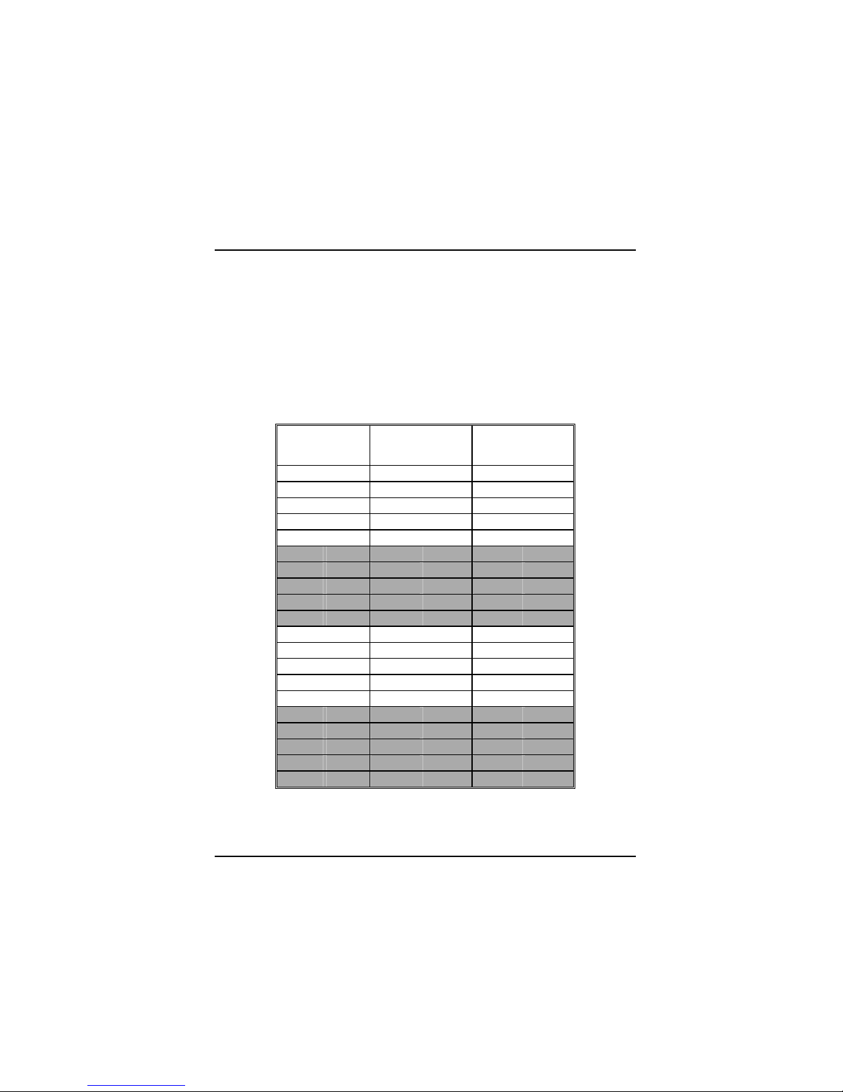
1.6.1 Front Panel Connector: JPANEL1
Pin Assignment Function Pin Assignment Function
No.
No.
1
Speaker
2
Sleep Control Sleep
3
NC
4
Ground Button
5
Ground
6
NA
7
5V
Speaker
Connector
8
Power LED (+)
9
HDD LED (+) Hard Disk
10
Power LED (+)
11
HDD LED (-) LED
12
Power LED (-)
POWER
LED
13
Ground Reset 14Power Button POWER
15
Reset Control Button
16
Ground Button
17
NA
18
KEY
19
NA
20
KEY
21
5V
22
Ground
23
IRTX
IrDA
Connector
24
IRRX
IrDA
Connector
Speaker Connector
An offboard sp eak er can be installed on the motherbo ard as a manufacturing option .
It can be c onnected to the motherboar d at the fr ont panel c onnector. Th e speaker
(onboard or offboard) provid es error beep code infor mation during t he Power On
Self-Test wh en the computer cannot use the video int erface. The sp eaker is not
connected to the audio subsystem and does not receive output from the audio
subsystem.
SPEK
P-LED
PWR
K
E
Y
HDLED
IrDA
NA
SLP
(-)(+)
(-)(+) (+)
N
A
REST
2
1
24
23
IrDA
 Loading...