


M7TDB
Federal Communications Commission
(F.C.C.) Statement
This device complies with Part 15 of the FCC Rules. Operation of this device is
subject to the following two conditions: (1) this device may not cause harmful
interference, and (2) this device must accept any interference received, including
interference that may cause undesired operation.
Accessories: This device has been tested and found to comply with the limits of a
Class B digital device, the accessories associated with this equipment are as
follows:
1. Shielded serial cable. (Can be obtained from multiple retail outlets)
2. Shielde d prin te r ca ble. (Can be o bta i ne d fr o m m ul ti ple retail out le t s )
3. Shielded video cable. (Can be obtained from multiple retail outlets)
4. Shielded pow er cord. (Pr o vided by manufac tur e r )
These accessori es are required to ensure complianc e with FCC Rules. It is the
responsibility of the user to provide and use these accessories properly.
This equipment has been tested and found to comply with the limits of a Class B
digital device, pu rs uan t to Pa rt 1 5 of th e FCC R ul es. Th ese l i mits ar e d esign ed to
provide reasonable protection against harmful interference in a residential
installation. This equipment generates, uses and can radiate radio frequency
energy and, if not installed and used in accordance with the instructions, may
cause harmful in terference to rad io communications. Th ere is no guarantee t hat
interference will not occur in a particular installation. If this equipm ent does cause
harmful interference to radio or television reception, which can be determined by
turning the equipment off and on, you are encouraged to try to correct the
interference by one or more of the following measures:
1. Reorient / relocate the receiving antenna.
2. Increase the separation between the equipment and receiver.
3. Connect the equipment into an outlet on a circuit different from that to which
the receiver is connected.
4. Consult the de a ler or an exper ie nc ed radio/TV te chni c ian fo r hel p.
Caution: Changes or modifications not expressly approved by the manufacturer
could void the user’s authority to operate the equipment.

Disclaimer
The vendor mak es no representations or warranties with resp ect to the contents
here of and specially disclaims any implied warranties of merchantability or
fitness for any purpose. Further the vendor reserves the right to revise this
publication and to make changes t o the contents here of without obligation t o
notify any party beforehand.
Duplication of this publication, in part or in whole, is not allowed without first
obtaining the vendor’ s appro v a l in wr it in g.
Trademarks and Remarks
MS-DOS, Windows, Windows NT, Windows 9X, Windows ME, Windows XP
and Windows 2000 are products of Microsoft Corp, with its ownership of
trademark, and are distributed by the vendor under a license agreement.
All trademarks used in this manual are the property of their respective owners.
Copyright© 2001
All Rights Reserv e d
Canadian D.O.C. Statement
This digital apparatus does not exceed the Class B limits for radio noise emissions
from digital apparatus as set out in the radio interference regulations of the
Canadian Depar tm ent of Comm unic a tio ns.
Cet appareil numbérique n‘émet pas de bruits radioélectriques dépassant les
limites appliquées aux appareils numbériques de Class B préscrits dans le
réglement du brouillage radioélectrique edict par le minister Des Communications
du Canada.

Contents
i
Introduction ..................................................................................1-1
1. Motherboard Description ............................. ........................ ...1-2
1.1 Features...................................................................................................1-2
1.1.1 Hardw ar e... ...... ........ ....... ...... ...... ........ ....... ...... ...... ........ ....... ...... ...... ......... ...... ..1-2
1.1.2 BIO S................... ...... ..... .... .... ...... .... .... ..... .... ...... .... ..... .... ...... .... .... .... ....... .... ....1-7
1.1.3 So ftwa re................ .... ....... .... .... .... ...... ..... .... .... .... ...... ..... .... .... ...... .... .... ..... ...... ..1-7
1.1.4 Acc esso ries........................ ...... ...... ...... ......... ...... ...... ....... ........ ...... ...... ....... ......1-7
1.2 Motherboard Installation.........................................................................1-8
1.2.1 Sy st em Bloc k D iag ram......... .... .... .... ....... .... .... .... ...... ..... .... .... ...... .... ..... .... ......1-8
1.2.2 Layout of Mo ther b oa rd......... .... .... ...... ..... .... .... ...... .... ..... .... ...... .... .... ..... ...... ....1-9
1.2.3 Quick Re fere nce............ ...... ...... ...... ......... ...... ...... ...... ......... ...... ...... ......... ......1-10
1.3 CPU Installation....................................................................................1-11
1.3.1 CPU I nst alla tion P roce dure : Soc ket 478............ ........ ....... ........ ...... ....... ......1-11
1.3.2 CPU F an He ade r: JCF AN1.......... ......... ...... ...... ........ ....... ...... ........ ....... ...... ..1-12
1.3.3 Sy st em Fa n H ea der: JS FA N1............. .... .... .... ...... .... ..... ...... .... .... .... ....... .... ..1-12
1.4 RAM Module Installation .....................................................................1-13
1.4.1 DIMM............. ...... ....... ........ ...... ...... ....... ........ ...... ...... ......... ...... ...... ...... .........1-13
1.4.2 How to ins ta ll a DIMM Modu le........................... ...... ....... ........ ...... ....... ......1-15
1.5 Slots ......................................................................................................1-16
1.5.1 AGP ( Acce lera ted Gra phic s Por t) S lot................... ....... ........ ...... ...... ......... ..1-17
1.5.2 CNR (C om mu nic ati on Ne tw ork Ri s er) Slot.............. ..... .... ...... .... .... ....... ....1-17
1.5.3 PCI ( Per iphe ral C ompo nent Inte rcon nec t) Slo ts...... ....... ...... ........ ...... .........1-17
1.6 Connectors, He aders & Jumpers...........................................................1-18

Contents
ii
1.6.1 Fr ont Pa ne l C on nec to r: JP AN EL 1....................... ...... ..... .... .... ...... .... ..... ......1-19
1.6.2 ATX 20-p in Pow er Co nnec tor: JAT XPWR 1........ ......... ...... ...... ......... ...... ..1-21
1.6.3 ATX 12V Po wer C onne ct or: JA TXP WR2............. ....... ...... ........ ....... ...... ..1-21
1.6.4 AUX P ower Conn ect or : JAUXP WR1. ........ ...... ........ ....... ........ ...... ....... ......1-21
1.6.5 Hard Di sk Con nec tors : IDE 1/ID E2.............. ...... ...... ......... ...... ...... ......... ......1-22
1.6.6 Flo ppy Disk C onne cto r: FD C1..................... ........ ....... ...... ...... ........ ....... ......1-22
1.6.7 Wake On LAN Hea der : JWO L1.................... ...... ....... ........ ...... ...... ....... ......1-22
1.6.8 Cle ar C MOS Ju mpe r : JC M OS1....................... .... .... ....... .... .... ...... .... ..... .... ..1-23
1.6.9 Fr ont USB Hea der s: JU SBF1 / JUSB F2 ( O pti ona l)........................ ..... .... ....1-23
1.7 Peripheral Port.......................................................................................1-24
1.7.1 PS/2 Mo use / Key board Co nnector : JKBMS1................. ........ ........... ........1-24
1.7.2 USB C onne cto r: JUS B1................. ....... ...... ...... ........ ....... ...... ...... ........ ....... ..1-25
1.7.3 Ser ial a nd Pa ral lel I nte rfac e Por ts. ...... ....... ........ ...... ....... ........ ...... ...... ....... ....1-26
1.7.3.1 The Serial Interface: JCOM1/ JCOM2........................ .. .. .. .... .. .. ... .... .. .. .. .1-26
1.7.3.2 Parallel Interface Port: JPRNT1 ....... .. .... .. .. .... .. ... .. .... .. .. .. .... .. .. ..... .. .. .. .... .1-28
1.7.4 Game (Joy stic k/MI DI) Port Con necto r: JG AME1.................. ...... ....... ......1-29
1.7.5 Aud io Po rt Con nec tors : JSP KR1/ JLIN1 /JMI C1.......... ...... ........ ...... ......... ..1-29
1.7.6 Aud io Su bsy stem............ ........ ...... ....... ...... ........ ...... ....... ...... ........ ...... ....... ....1-30
1.7.6.1 CD-ROM Audio-In Header: JCD1........................ .... .. .. .... .. .. .. .... ... .. .... .. .1-30
1.7.6.2 CD-ROM Audio-In Header: JCD2........................ .... .. .. .... .. .. .. .... ... .. .... .. .1-31
1.7.6.3 Front Audio Header: JAUDIO1(Optional) ......... .. .... .. .. .... .. .. .. .... ... .. .... .. .1-31
1.7.6.4 Telephony Audio Header: JTAD1....................... .. .... .. .. .. .... .. .. ..... .. .. .. .... .1-31
1.7.6.5 Auxiliary Audio Header: JAUX1(Optional)............... .. .... .. .. .. ..... .. .. .... .. .1-31
2. BIOS Setup.............. ........................ ..........................................2-1

Contents
iii
2.1 Main Menu..............................................................................................2-3
2.2 Standard CMOS Features........................................................................2-6
2.3 Advanced BIOS Features........................................................................2-9
2.4 Advanced Chipset Features....... .. .. .. ................... .. .................. .. .............2-13
2.5 Integrated Peripherals ...........................................................................2-16
2.6 Power Management Setup.....................................................................2-21
2.7 PnP/PCI Configurations........................................................................2-26
2.8 PC Health Status ...................................................................................2-29
2.9 Frequency/Voltage Control...................................................................2-31
3. RAID BIOS Setting (Optional)................................................3-1
3.1 Getting Started ........................................................................................3-1
3.1.1 Intr oduc tion. ...... ...... ......... ...... ...... ...... ......... ...... ...... ....... ........ ...... ...... ......... ......3-1
3.1.2 Ma in F ea t ure s & Be ne fi ts........... .... ..... ...... .... .... .... ....... .... .... .... ...... .... ..... ...... ..3-1
3.2 Installation of Driver...............................................................................3-2
3.2.1 Intr oduc tion. ...... ...... ......... ...... ...... ...... ......... ...... ...... ....... ........ ...... ...... ......... ......3-2
3.2.2 Win dows 98/ME............... ...... ...... ......... ...... ...... ........ ....... ...... ...... ......... ...... ....3-2
3.2.3 Win dows NT 4.0.......... ...... ........ ...... ....... ...... ........ ...... ....... ...... ........ ...... ....... ....3-4
3.2.4 Win dows 2000................ ...... ...... ........ ....... ...... ........ ....... ...... ...... ........ ....... ......3-6
3.3 Use RAID Administrator ........................................................................3-8
3.3.1 Ins tall R AID Admi nist rato r................. ........ ...... ...... ......... ...... ...... ......... ...... ....3-8
3.3.2 Ru n R AID Ad m inis tr a tor................. ....... .... .... .... ...... ..... .... .... ...... .... ..... .... ......3-9
3.3.3 Crea t e S tr ipe A rr ay (R AID 0, fo r Pe rf orm anc e)......... .... .... ...... .... .... ..... ......3-10
3.3.4 Crea t e M ir ror A rray (RAID 1, f or Da ta P rot ec tio n)................... ...... ..... .... ..3-15

Contents
iv
3.3.5 Add /Remov e S par e Disk.......... ...... ....... ...... ........ ....... ...... ...... ........ ....... ...... ..3-20
3.3.6 Sy nch ro niz e/V al id ate /Ve rif y Mi rro r A rr ay........ ...... ..... .... ...... .... .... ..... ...... ..3-21
3.3.7 Cre at e S pa n Arr ay................. .... .... .... ....... .... .... .... ...... ..... .... .... ...... .... .... ..... ....3-23
3.3.8 Create 0+1 Array (For Performance & Data Protection)............................3-24
3.3.9 Re mov e D isk A rra y...................... .... ....... .... .... .... ...... ..... .... .... ...... .... .... ..... ....3-27
3.3.10 Set Tra nsf er Mo de.... ....... ...... ........ ....... ...... ...... ........ ....... ...... ...... ......... ...... ..3-28
3.3.11 D ev ice S tat us............... ...... .... .... .... ....... .... .... .... ...... ..... .... .... .... ...... .... ..... .... ..3-29
3.3.12 Ho t-swa ppi ng Ha rd D isks of Mi rro r Arr ay.... ...... ......... ...... ...... ...... ......... ..3-30
3.3.13 E ve nt Log............... ..... .... ...... .... .... .... ....... .... .... .... ....... .... .... .... .... ...... ..... .... ..3-31
3.4 BIOS Configuration..............................................................................3-32
3.4.1 En ter in to BIOS Con figu rat ion Ut ility.. ...... ........ ...... ......... ...... ...... ......... ......3-32
3.4.2 Cre at e R AI D......... ....... .... .... .... .... ...... ..... .... .... ...... .... .... ..... .... ...... .... .... ..... ......3-33
3.4.3 Dele te R AID......... ....... ...... ........ ...... ....... ...... ........ ...... ....... ...... ........ ...... ....... ..3-34
3.4.4 Re bu ild M irr or Arr ay............ .... .... .... ....... .... .... .... ...... ..... .... .... ...... .... ..... .... ....3-34
3.4.5 Add S pare Di sk................. ........ ...... ....... ...... ........ ...... ....... ...... ........ ....... ...... ..3-35
3.4.6 Remo ve S pare Disk................ ...... ....... ........ ...... ...... ....... ........ ...... ...... ......... ..3-35
3.4.7 Set D isk M ode............... ...... ...... ...... ......... ...... ...... ...... ......... ...... ...... ......... ......3-35
3.4.8 Se t B oo t D isk ........ ....... .... .... .... ...... .... ..... .... ...... .... .... ..... ...... .... .... .... ....... .... ....3-36
4. T r ouble Shooting.......................................................................4-1

Chapter 1 Motherboard Description
1-1
Introduction
System Overview
Congratulations on the purchase of your new system! This motherboard is des igned
to take advantage of the latest industry technology to provide you with the ultimate
solution in data proc essing. I n the tradition o f it s predeces s o rs, this moth e rbo a rd
continues a commitment to reliability and performance and strives for full compliance
and compatibility with industry software and hardware standards.
M7TDB Highlights:
8 Contains on board I/O facilities, which include two serial ports, a parallel port, a PS/2
mouse po rt, a PS/2 keyboard port, audio ports, USB port s and a game port.
8 Contains on b oard IDE facilities for IDE devices such as hard d isks and CD-ROM
Drives.
8 Supports the Int el P entiu m 4
®
(Socket 478) processor, a leading edge processor which
brings to you the latest technology in micro architecture design, graphics performance,
system bus design, cache architecture and much more.
8
Complies with PC ATX form factor specifications.
8 Supports pop ular operatin g syst ems such as W ind ows 95 /98, W indow s NT, Window s
2000, Windows ME, Novell, UNIX, LI NU X and SCO UNIX.

Chapter 1 Motherboard Description
1-2
1. Motherboard Description
1.1 Features
1.1.1 Hardware
CPU
− Provides So ck e t- 478.
− The Intel Pentium
®
4 processor the new geheration power for high-end
workstations and servers.
Speed
− Runing at 400 MHz Front Side Bus frequency.
− Supports up to 2.4 GHz CPU core speeds.
− The 33MHz 32 bit PCI 2.2 com p li a nt.
− The 66MHz AGP 2.0 compliant interface supports 1x, 2x and 4x data
transfer mode. (Supports only 1.5v AGP electricals.)
Chipset
− Chipset– Intel 82845/82801BA.
− Chipset – Winbond W83627HF.

Chapter 1 Motherboard Description
1-3
DRAM Memo r y
− Supports 100MHz or 133MHz SDR SDRAM de v i ce s .
− Supports 64Mb, 128Mb, 256Mb and 512Mb technologies for x8 and 16
devices
− Max of 3 Double-Sided DIMMs (6 rows populated) with unbuffered
PC133 (with or without ECC).
− The larg e st m emory ca pa c ity po ss i ble is 3 GB .
− Maximum memory bandwidth of 1GB with PC133.
Shadow RAM
− Motherboard is equipped with a memory controller providing shadow
RAM and support for ROM BIOS.
Green Functionality
− Supports Award BI OS™ power manag e ment functio nal ity .
− Has a power do wn tim er from 1 to 15 mi nute s .
− Wakes from power saving sleep mode with any keyboard or mouse
activity.
BUS Slots
− (1) AGP slot.
− (1) CNR slot.
− (6) 32-bit PCI bus slots
Flash Memory
− Supports flash memory functionality.
− Supports ESCD functio na lit y .

Chapter 1 Motherboard Description
1-4
Built in IDE F acilities
− Supports four IDE hard disk drives.
− Supports PIO Mode 4, Master Mode, and high performance hard disk
drives.
− Supports disk tra ns fer rates up to 100 MB/s econd.
− Supports Ultra DMA 33, Ultra DMA 66, Ultra DMA 100 Bus Master
Modes.
− Supports IDE interface with CD-ROM.
− Supports high ca pa ci ty har d disk dr iv es.
− Supports LBA mode.
AC’97 Sound Codec Onboard
− AC-LINK protocol comfliance.
− Complia nt with AC ’97 2. 2 spe c i fic a tio n.
− 18-bit full duplex stereo ADC,DACs.
− SNR>95 Bb throug hmixer and DAC.
− AC-3 playback required for PVD applications.
Universal Serial Bus
− Supports two back panel Universal Serial Bus Ports and two front panel
Universal Serial Bus Ports (optional).
− Supports 48 MHz USB.
Hardware Monitor Function
− Monitors CPU Fan Speed.
− Monitors System Voltage.

Chapter 1 Motherboard Description
1-5
HPT370 is designed to enable you add high performance ATA/ATAPI
devices. (Optional)
− Ultra DMA 100MB/S operation per ATA channel.
− Support up to 66MHz PCI bus Cloc k .
− One PCI functio n s upport s two independent ATA cha nne l s.
− Dedicated ATA Bus.
− ATA clock inde pendent from PCI bus.
− Optional between external 50Hz ATA bus clock or internal PLL.
− 256Byte FIFO per ATA channel.
− Large FIFO independent.
− Easy Plug-a nd-P lay feature.
− Supports up to 4 IDE de vic e s . (C o exi s t with o n-bo ar d ID E)
− Supports Hard Drive with capacity larger than 30GB.
− RAID functio n su pport ed (RAID 0,1, 0+1) .
− Supports the most popular Windows 95/98,Windows NT4.0, Windows
2000, Windows ME and Linux.
− Supports booting function with Flas h Me mory inte rfa c e .
− Automatically fine tunes to the best performance for each IDE/ATAPI
device.
− Concurre nt PIO and bus master access(ATA port acce ssible during DMA
transfer)
− Total ATA b us tr i-stat e by ext erna l con trol an d S uppor ts Hot swap (Low
signal Current).
Dimensions (ATX form-facto r)
− 24.4cm x 30.5cm (W xL).

Chapter 1 Motherboard Description
1-6
Super I/O Built-in onboard
− Support one m ult i- m o de Pa ra llel Port.
(1) Standard & Bidirection Parallel Port (SPP).
(2) Enhanced Parallel Port (EPP).
(3) Extended Capabilities Port (ECP).
− Supports two serial ports, 16550 UART wit h 16 byte FI FO .
− UART data rate s up to 1. 5 Mbaud.
− Supports one I nf r ared transmi ss i on (I R ) po r t.
− Supports PS/2 Mouse /Keyboa rd.
− Supports 360KB, 720KB, 1.2MB, 1.44MB and 2.88MB floppy disk
drives.

Chapter 1 Motherboard Description
1-7
1.1.2 BIOS
− AWARD legal BIOS.
− Supports APM1.2.
− Supports USB Function.
− Supports ACPI.
1.1.3 Software
Operating System
− Offers the hi ghest performance for MS-DOS, Windows NT, W indows
2000, Windows 95/98, Windows ME, Windows XP, Novell, LINUX,
UNIX, SCO UNIX etc.
1.1.4 Accessories
− HDD Cable.
− FDD Cable.
− Flash Memory Writer for BIOS Update.
− USB Cable (Optiona l).
− Rear I/O Panel for ATX Case (Optional).
− Fully Setup Drive r CD.
Chapter 1 Motherboard Description
1-8
1.2 Motherboard Installation
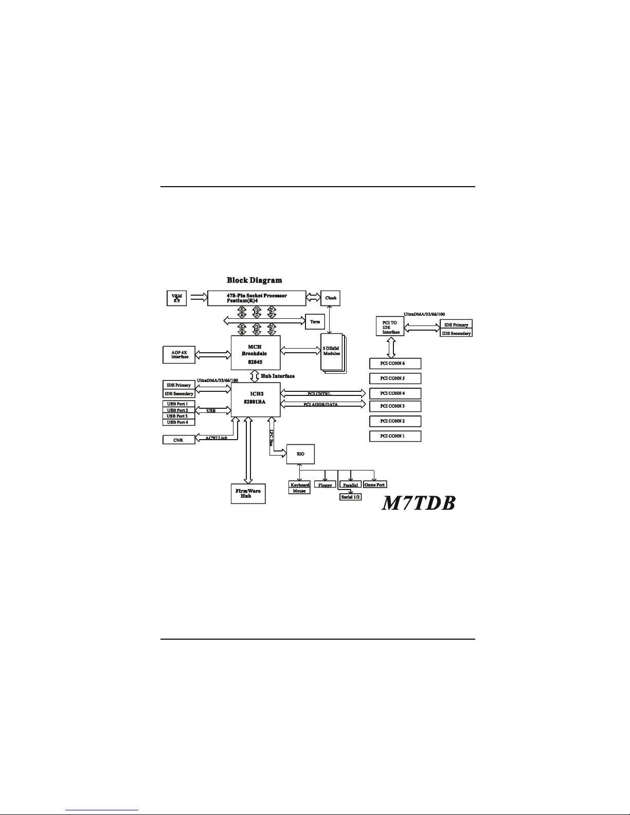
1.2.1 System Block Diagram

Chapter 1 Motherboard Description
1-9
1.2.2 Layout of Motherboard
Model No.M7TDB
JAUDIO1
JATXPWR2
U13
K/B
&
Mouse
JUSB1
USB
COM1COM2
Parallel Port
JSPKR1
SP-OUT
JLIN1
LINE-IN
JMIC1
MIC-IN
GAME Port
JKBMS1
JCOM1
JCOM2
JPRNT1
JGAME1
1
1
JLIN1
LINE-IN
JMIC1
1
I/O
1
1
13
1
24
12
BAT1
U12
82845
U11
82801BA
JCMOS1
JWOL1
IDE2
IDE1
RAID2
RAID1
FDC1
JPANEL1
High Point
HPT370A
U21
1
1
SECONDARY IDE CONN.
PRIMARY IDE CONN.
FWH
BIOS
PCI5
PCI6
PCI4
PCI3
PCI2
PCI1
PCI BUS SLOT
PCI BUS SLOT
PCI BUS SLOT
PCI BUS SLOT
PCI BUS SLOT
PCI BUS SLOT
CNR BUS SLOT
AGP BUS SLOT
AGP1
JATXPWR1
JCFAN1
1
CNR1
1
JTAD1
JAUX1
JCD1
JCD2
JUSBF1
1
JSFAN1
1
1
JUSBF2
RAID1 IDE CONN.
RAID1 IDE CONN.
RAID IDE CONN.
RAID IDE CONN.
U1
Socket 478
DIMM1
DIMM2
DIMM3
DIMM4
FLOPPY DISK CONN.
2
4
3
JAUXPWR1

Chapter 1 Motherboard Description
1-10
1.2.3 Quick Reference
A. Back Panel I/O Connectors L. Front Panel Connector (JPANEL1)
B. Front Audio Header (*JAUIO1) M. Floppy Disk Connector (FDC1)
C. ATX12V Power Connector N. Wake-On-LAN Header (JWOL1)
(JATXPWR2) O. RAID Conn. (*RAID1/2)
D. CD Audio-In Headers (JCD1/2) P. Clear CMOS Jumper (JCMOS1)
E. Au xiliary Audio Header (*JAUX1) Q. IDE Connectors (IDE1/2)
F. Telephony Audio Header (JT AD1) R. AUX Power Connector (JAUXPWR1)
G. CNR Slot (CNR1) S. ATX Main Power Connector
H. PCI BUS Slots (PCI1-6) (JATXPWR1)
I. System FAN Header (JSFAN1) T. DIMMs (DIMM1/4)
J. Front USB Header (*JUSBF2) U. CPU FAN Header (JCFAN1)
K. Front USB Header (*JUSBF1) V. AGP Slot (AGP1)
NOTE: The “ * “mark represent t he f unction is optional.
ABEF G
H
I
J
K
L
M
N
OP
Q
R
T
U
CD
S
V

Chapter 1 Motherboard Description
1-11
1.3 CPU Installation
1.3.1 CPU Installation Procedure: Socket 478
1. Pull the lever sid eways away fr om the socket then raise the lever up to a
90-degre e a ng le.
2. Locate Pin A i n t h e s ocket and lo ok for the white d ot or cu t edge i n t he CPU .
Match Pin A with the white dot/cut edge then insert the CPU.
3. Press the le v e r dow n.
4. Put the fan on the CPU and buckle it and put the fan’s power-port into the
JCFAN1, then to complete the installation.
C
P
U
Socket 4 78

Chapter 1 Motherboard Description
1-12
CPU Installation Layout
1.3.2 CPU Fan Header: JCFAN1
Pin No. Assignment
1
Ground
2
+12V
3
Sense
1.3.3 System Fan Header: JSFAN1
Pin No. Assignment
1
Ground
2
+12V
3
Sense
JCFAN1
1
1
JSFAN1

Chapter 1 Motherboard Description
1-13
1.4 RAM Module Installation
1.4.1 DIMM
DRAM Access Time : 3.3V Unbuffered SDRAM PC100/133 Type re quired.
DRAM Type: 64MB/ 128MB/ 256MB/512MB D IMM Module
(168 pin)
Total Bank 0 Bank 1 Bank 2
Memory Size (MB) DIMM1 DIMM2 DIMM3/4
64 M 64M x 1 pc ---- ---128 M 128M x 1 pc ---- ---256 M 256M x 1 pc ---- ---512 M 512M x 1 pc
128 M 64M x 1 pc 64M x1 pc ---256 M 128M x 1 pc 128M x 1 pc ---512 M 256M x 1 pc 256M x 1 pc ----
1024 M 512M x 1 pc 512M x 1 pc ----
192 M 64M x 1 pc 64M x1 pc 64M x 1 pc
320 M 128M x 1 pc 128M x 1 pc 64M x 1 pc
576 M 256M x 1 pc 256M x 1 pc 64M x 1 pc
1088 M 512M x 1 pc 512M x 1 pc 64M x 1 pc
256 M 64M x 1 pc 64M x1 pc 128M x 1 pc
384 M 128M x 1 pc 128M x 1 pc 128M x 1 pc
640 M 256M x 1 pc 256M x 1 pc 128M x 1 pc
1152 M 512M x 1 pc 512M x 1 pc 128M x 1 pc
384 M 64M x 1 pc 64M x1 pc 256M x 1 pc
512 M 128M x 1 pc 128M x 1 pc 256M x 1 pc
768 M 256M x 1 pc 256M x 1 pc 256M x 1 pc
1280 M 512M x 1 pc 512M x 1 pc 256M x 1 pc
640 M 64M x 1 pc 64M x1 pc 512M x 1 pc
768 M 128M x 1 pc 128M x 1 pc 512M x 1 pc
1024 M 256M x 1 pc 256M x 1 pc 512M x 1 pc
1536 M 512M x 1 pc 512M x 1 pc 512M x 1 pc

Chapter 1 Motherboard Description
1-14
Install DIMM3/4 in any combination table:
DIMM3 DIMM4
Double X
X Double
Single Single
* This M7TDB mothe rboard does not suppor t with parity DIMM.
*The list shown above for DRAM configuration is only for reference.
Note: 1. Don't stuff or remove the DIMM memory, if the LED1 is
lighting.
2. When you’re using single- sided memory on DIMM4, you
must use single-sided memory on DIMM3. If you use
double-sided memory on DIMM3, please do not insert any
memory on DIMM4 and vice versa.

Chapter 1 Motherboard Description
1-15
1.4.2 How to install a DIMM Module
1. The DIMM socket has a “ Plastic
Safety Tab” and the DIMM memory
module has an asymmetrical notch”,
so the DIMM memory module can
only fit into the slot in one direction.
2. Push the tabs out. Insert the DIMM
memory modules into the s ocket at a
90-degree angle then push down
vertically so that it will fit into place.
3. The Mounting Holes and plastic
tabs should fi t over the edge and hold
the DIMM memory modules in place.

Chapter 1 Motherboard Description
1-16
1.5 Slots
The slots in this mot h erbo ar d are designed to hold expansion cards and connect them to
the system bu s. Ex pansi on sl ots ar e a m eans of add ing or enhanci ng th e moth erboard 's
features and capabilities. With these efficient facilities, you can increase the
motherboard's cap abilities by adding hard ware that performs task s that are not part of
the basic system.
AGP Slot
PCI Slots
CNR Slot

Chapter 1 Motherboard Description
1-17
1.5.1 AGP (Accelerated Graphics Port) Slot
Unlike the mouse ports, keyboard ports and printer ports this motherboard does not
have built in video facilities and therefore requires a video card for one of the
expansion slots. Your monitor will attach directly to that video card. This
motherboard supports video cards for PCI and ISA slots but is also equipped with
an Accelerated Graphics Port (AGP). An AGP card will take advantage of AGP
technology for improved video efficiency and performance, especially with 3D
graphics.
1.5.2 CNR (Communication Network Riser) Slot
The CNR specifi c ation is an open In d u stry Standard Arch itectu r e and that defin es a
hardware scal able riser card interfac e, which su pports audi o, network a nd modem
only.
1.5.3 PCI (Peripheral Component Interconnect) Slots
This motherboard is equipped with 6 standard PCI slots. PCI stands for Peripheral
Component Interconnect and is a bus standard for expansion cards, which has, for
the most part, su pp lant ed the old er ISA b us stan dar d. Th is PC I sl ot is d esigna ted as
32 bit.

Chapter 1 Motherboard Description
1-18
1.6 Connectors, Headers & Jumpers
The connectors, headers and jumpers introduced below provide you lots of
capabilities such as power supply, front panel signal revelation, IDE hard disk
connection, floppy disk connection, Wake On LAN function and Front USB
connection. Notic eably, a jumper has two or more pins that can be covered by a
plastic jumper cap, allowing you to select different system options.
JATXPWR2
1
JATXPWR1
1
JCMOS1
JWOL1
IDE1
FDC1
JPANEL1
1
JUSBF1
1
JUSBF2
2
3
4
IDE2
JAUXPWR1
1

Chapter 1 Motherboard Description
1-19
1.6.1 Front Panel Connector: JPANEL1
Pin Assignment Function Pin Assignment Function
No.
No.
1
Speaker 2 Sleep Control Sl eep
3
NC Speaker 4 Ground Button
5
Ground Connector
6
NA NA
7
+5V 8 Power LED (+)
9
HDD LED (+) Hard Disk
10
Power LED (+)
11
HDD LED (-) LED
12
Power LED (-)
POWER
LED
13
Ground Reset 14Power Button POWER
15
Reset Control Button
16
Ground Button
17
NA
18
KEY
19
NA
20
KEY
21
VCC5
22
Ground
23
IRTX
IrDA
Connector
24
IRRX
IrDA
Connector
Speaker Connector
An offboard sp eak er can be installed on the motherboard as a manufacturing op tion.
An offboard speaker can be connected to the motherboard at the front panel
connector. The speaker (onboard or offboard) provides error beep code information
during the P ower On Self-Test when t he comput er cann ot use th e vid eo interface.
The speaker is not connected to the audio subsystem and does not receive output
from the audio subsystem.
SPEK
PLED
PWR
K
E
Y
HDLED
IrDA
NA
SLP
(-)(+)
(-)(+) (+)
N
A
REST
2
1
24
23
IrDA

Chapter 1 Motherboard Description
1-20
Reset Button
This connector can b e attached to a moment ary S PS T swi tch. This switch is usually
open and when closed will cause the motherboard to reset and run the POST
(Power On Self Test).
Power LED Connector
This connector ca n be attached to an LED on the front panel of a computer c ase.
The LED will illuminate while the computer is powered on.
HDD LED (Hard Drive LED Connector)
This connector ca n be attached to an LED on the front panel of a computer c ase.
The LED will flicker du ring disk activity. T his disk activity on ly applies t o those
IDE drives directly attached to the system board.
IrDA (Infrared Connector)
This connector is used to attach to an infrared sensing device. After the IrDA
interface is con figured, connecti onless data transfer to and from portab le devices
such as laptops, PDAs is possible.
Sleep Button (Green Button)
This connector is used to conserve energy by powering down the monitor and the
hard disk when not in use. To configure this option, you need to connect a button
from the front panel to this connector. Depressing th e button will power down the
monitor and hard drives until the system is invoked by any keyboard activity,
mouse activity, modem activity or when the sleep button is depressed again. APM
(Advanced Power Ma na gement) must be enabled in th e syst em BI OS an d th e APM
driver must be loaded.
Power Button
This connector c an b e atta ched to a fr ont panel power switch. T he sw itch must pu ll
the Power Button pin to ground for at least 50 ms to signal the power supply to
switch on or off. (The time required is du e to internal d ebounce circuitry on t he
system board). At least two seconds must pass before the power supply will
recognize another on/off signal.

Chapter 1 Motherboard Description
1-21
1.6.2 ATX 20-pin Power Connector: JATXPWR1
This connector supports the power button on-board. Using the ATX power
supply, function such as Soft Power Off is supported on this motherboard. This
power connector supports instant power-on functionality, which means that the
system will boot up instantly when the power connector is inserted on the board.
PIN Assignment PIN Assignment
1 3.3V 11 3.3V
2 3.3V 12 -12V
3 Ground 13 Ground
4 5V 14 PS_ON
5 Ground 15 Ground
6 5V 16 Ground
7 Ground 17 Ground
8 PW_OK 18 -5V
9 5V_SB 19 5V
10 12V 20 5V
1.6.3 ATX 12V Power Connector: JATXPWR2
PIN Assignment PIN Assignment
1 +12V 3 Ground
2 +12V 4 Ground
1.6.4 AUX Power Connector: JAUXPWR1
PIN Assignment PIN Assignment
1 Ground 4 3.3V
2 Ground 5 3.3V
3 Ground 6 5V
Chapter 1 Motherboard Description
1-22
1.6.5 Hard Disk Connectors: IDE1/IDE2
The motherboard has a 32-bit Enhanced PCI IDE Controller that provides PIO
Mode 0~4, Bus Master, and Ultra DMA / 33, Ultra DMA / 66,Ultra DMA / 100
functionality. It has two HDD connectors IDE1 (primary) and IDE2 (secondary).
You can connect up to four hard disk drives, a CD-ROM, a 120MB Floppy
(reserved for future BIOS) and other devices to IDE1 and IDE2. These
connecto rs suppo r t the I D E hard disk ca bl e pro v ide d.
• IDE1 (Primary IDE Connector)
The first hard drive should always be connected to IDE1. IDE1 can connect a
Master and a Slav e drive. You must conf igure the second har d drive on IDE1 to
Slave mode by setting the jumper accordingly.
• IDE2 (Secondary IDE Connector)
The IDE2 controller can also support a Master and a Slave drive. The configuration
is similar to IDE1. The second drive on this controller must be set to slave mode.
1.6.6 Floppy Disk Connector: FDC1
The motherboard provides a standard floppy disk connector (FDC) that supports
360K, 720K, 1.2M, 1.44M and 2.88M floppy disk types. This connector supports
the provide d fl o ppy dri v e ribbo n c ables.
1.6.7 Wake On LAN Header: JWOL1
Pin No. Assignment
1
5V SB
2
Ground
3
Wake up

Chapter 1 Motherboard Description
1-23
1.6.8 Clear CMOS Jumper: JCMOS1
JCMOS1 Assignment
1 3
1-2 Closed
Normal Operation (default)
1 3
2-3 Closed
Clear CMOS Data
1.6.9 Front USB Headers: JUSBF1/JUSBF2 (Optional)
(JUSBF1)
Pin Assignment Pin Assignment
1
+5V(fused)
2
NC
3
USBP2-
4
Ground
5
USBP2+
6
USBP3+
7
Ground
8
USBP3-
9
NC
10
+5V(fused)
(JUSBF2)
Pin Assignment Pin Assignment
1
+5V(fused)
2
+5V(fused)
3
USB2 Data (-)
4
USB3 Data (-)
5
USB2 Data (+)
6
USB4 Data (+)
7
Ground
8
Ground
9
KEY
10
NA
Remove AC
power line
Wait five
seconds
JCMOS1
(1-2) closed
AC power on
Reset you r d es i re d pas s word
or clear CMOS data
JCMOS1
(2-3) closed

Chapter 1 Motherboard Description
1-24
1.7 Peripheral Port
1.7.1 PS/2 Mouse / Keyboard Connector: JKBMS1
The motherboard provides a standard PS/2 mouse / Keyboard mini DIN connector
for attaching a PS/2 mous e. You can plu g a PS/2 mou se / Keyboard directly into
this connector. The connector location and pin definition are s hown below:
PS/2 Mouse
Pin 5 Mouse Cloc k
Pin 6NC
Pin 4 VCC
Pin 6 NC
Pin 2 NC
Pin 4 VCC
Pin 2 NC
PS/2 Keyboard
Pin 1 KBD DATA
Pin 3 GND
Pin 5 KBD DATA
Pin 3 GND
Pin 1 Mouse DATA
PS/2 Mouse / Keyboard Connectors
Pin Assignment
1 Data
2 No connect
3 Ground
4 +5 V (fused)
5 Clock
6 No connect
PS/2
Keyboard
PS/2
Mouse
USB
COM1
Parallel
Game Port
Speaker
Out
Line In
Mic
In
JPRNT1
JGAME1
JCOM2JCOM1
JKBMS
1
JUSB1
JSPKR1 JLIN1 JMIC1
COM2
 Loading...