


M7SXF/H
Federal Communications Commission
(F.C.C) Statement
This device c omplies with Part 15 of the FCC Ru les. Operation of this devi ce is
subject to the following two conditions: (1) this device may not cause harmful
interference, and (2) this device must accept any interference received, including
interference that m ay cause undesired operation.
Accessories: This device has been tested and found to comply with the limits of a
Class B digital device; the accessories associated with this equipment are as
follows:
1. Shielded serial cable. (Can be obtained from multiple retail outlets)
2. Shielde d prin te r ca ble. (Can be o bta i ne d fr o m m ul ti ple retail outlets)
3. Shielded video cable. (Can be obtained from multiple retail outlets)
4. Shielded pow er cord. (Pr o vided by manufac turer)
These accessories are required to ensure compliance with FCC Rules. It is the
responsibility of the user to provide and use these accessories properly.
This equipment has been tested and found to comply with the limits of a Class B
digital device, pursuant of Part 15 of the FCC Rules. These limits are designed to
provide reasonable protection against harmful interference in a residential
installation. This equipment generates, uses and radiates radio frequency energy
and, if you did not installe d and use d in accorda nce wi th the instr uc t ions , may c a use
harmful interference in the radio communications. There is no guarantee that
interference will not occu r in a p articu lar instal lation. If t his equipment doe s caus e
harmful interference in the radio or television reception, which can be determined
by turning the equipment off and on, you are encouraged to try to correct the
interference by one or more of the following measures:
1. Reorient / relocate the receiving antenna.
2. Increase the separation between the equipment and the receiver.
3. Connect the equipment into an outlet from a different circuit where the
receiver is connected.
4. Consult the de a ler or an exper ie nc ed radio/TV te chni c ian fo r hel p.
Caution: Changes or modifications that is not expressly approved by the
manufacturer could void the user’s authority to operate the equipment.

Disclaimer
The vendor makes no representations or warranties with respect to the contents
and specially the vendor disclaims any implied
warranties of merchantability or
fitness for any purpose. Further the vendor reserves the right to revise this
publication and to make changes of the contents without obligation to notify any
party beforehand.
Duplication of this publication, in part or in whole, is not allowed without first
obtaining the vendor’s approval in wr iti ng .
Trademarks and Remarks
MS-DOS, Windows, Windows NT, Windows 9X, Windows ME, Windows XP
and Windows 2000 are products of Microsoft Corp, with its ownership of
tradema rk , a nd are distributed by the v e ndo r unde r a l icense agreement.
All trademarks used in this manual are property of their respective owners.
Copyright© 2001
All Rights Reserved
Canadian D.O.C. Statement
Th is digital app arat us does not exceed the Class B limits for ra d i o n oi s e emissions
from digital apparatus to set out of the radio interference regulations of the
Canadian Depar tm ent of Communications.
Cet appareil numbérique n‘émet pas de bruits radioélectriques dépassant les
limites appliquées aux appareils numériques de Class B préscrits dans le réglement
du brouillage radi o é le c t rique edict par le m inis t e r Des Communications du Canada .

Contents
i
Introduction ..................................................................................1-1
1. Motherboard Description ............................................ ............1-2
1.1 Features...................................................................................................1-2
1.1.1 Hardw ar e... ...... ........ ....... ...... ...... ........ ....... ...... ...... ........ ....... ...... ...... ......... ...... ..1-2
1.1.2 BIO S....................... ..... .... .... .... ...... .... ..... .... ...... .... .... ..... ...... .... .... .... .... ....... .... ..1-5
1.1.3 So ftwa re................ .... ....... .... .... .... ...... ..... .... .... .... ...... ..... .... .... ...... .... .... ..... ...... ..1-5
1.1.4 Acc esso ries........................ ...... ...... ...... ......... ...... ...... ....... ........ ...... ...... ....... ......1-5
1.2 Motherboard Installation.........................................................................1-6
1.2.1 Sy st em Bloc k D iag ram......... .... .... .... ....... .... .... .... ...... ..... .... .... ...... .... ..... .... ......1-6
1.2.2 Layout of Motherb oard..... .... .... ...... .... ..... .... ...... .... .... ..... ...... .... .... .... ..... ...... ....1-7
1.2.3 Quic k Re fere nce.......... ........ ...... ...... ....... ........ ...... ...... ....... ........ ...... ...... ....... ....1-8
1.3 CPU Installation......................................................................................1-9
1.3.1 CPU I nst alla tion P roce dure : Soc ket 478................ ....... ...... ........ ....... ...... ......1-9
1.3.2 CPU F an He ade r: JCF AN1.......... ......... ...... ...... ........ ....... ...... ........ ....... ...... ..1-10
1.3.3 Sy st em Fa n H ea der: JS FA N1............... .... .... ...... .... ..... .... ...... .... .... .... ....... ....1-10
1.4 RAM Module Installation .....................................................................1-11
1.4.1 DIMM............. ...... ....... ........ ...... ...... ....... ........ ...... ...... ......... ...... ...... ...... .........1-11
1.4.2 How to ins ta ll a DIMM Modu le........................... ...... ....... ........ ...... ....... ......1-12
1.5 Slots ......................................................................................................1-13
1.5.1 ACR (Adva nced Com munic ati on R iser) Slot.................... ...... ...... ......... ....1-14
1.5.2 AGP ( Acce lera ted Gra phic s Por t) S lot................... ....... ........ ...... ...... ......... ..1-14
1.5.3 CNR (C om mu nic ati on Ne tw ork Ri s er) Slot................. .... .... .... ...... .... ..... ....1-14
1.5.4 PCI ( Per iphe ral C ompo nent Inte rcon nec t) Slo ts...... ....... ...... ........ ...... .........1-14

Contents
ii
1.6 Connectors, He aders & Jumpers...........................................................1-15
1.6.1 Fr ont Pa ne l C on nec to r: JP AN EL 1......................... ....... .... .... ...... .... ..... .... ....1-16
1.6.2 ATX 20-p in Pow er Co nnec tor: JAT XPWR 1........ ......... ...... ...... ......... ...... ..1-18
1.6.3 ATX 12V Po wer C onne ct or: JA TXP WR2................ ...... ...... ........ ....... ......1-18
1.6.4 AUX P ower Conn ect or : JAUXP WR1. ........ ...... ........ ....... ........ ...... ....... ......1-18
1.6.5 AUX P ower Conn ect or : JAUXP WR2. ........ ...... ........ ....... ........ ...... ....... ......1-19
1.6.6 Hard Di sk Con nec tors : IDE 1/ID E2.............. ...... ...... ......... ...... ...... ......... ......1-19
1.6.7 Flo ppy Disk C onne cto r: FD D1............. ...... ...... ........ ....... ...... ...... ......... ...... ..1-19
1.6.8 Wake On LAN Hea der : JWO L1.................... ...... ....... ........ ...... ...... ....... ......1-20
1.6.9 Cle ar C MOS Ju mpe r : JC M OS1....................... .... .... ....... .... .... ...... .... ..... .... ..1-20
1.6.10 Front USB Headers: JUSB1/JUSB2 & USB20A1/USB20B1 (Optional)1-21
1.6.11 D IMM P owe r V ol tag e S el ec ti on: JD IM MP WR1................... .... ....... .... ..1-22
1.7 Peripheral Port.......................................................................................1-23
1.7.1 PS/2 Mo use / Key board Co nnector : JKBMS1................. ........ ........... ........1-23
1.7.2 USB & LAN C onne cto rs: J USBL AN1........................ ...... ........ ...... ....... ....1-24
1.7.3 VGA C onn ector : JVGA 1................. ......... ...... ...... ......... ...... ...... ........ ....... ....1-25
1.7.4 Ser ial a nd Pa ral lel I nte rfac e Por ts. ...... ....... ........ ...... ....... ........ ...... ...... ....... ....1-26
1.7.4.1 The Serial Interface: JCOM1/ JCOM2................ .. .. .. .... .. .. .. .... .. ... .... .. .. .. .1-26
1.7.4.2 Parallel Interface Port: JPRNT1 ........... .... .. .. .... ... .. .. .... .. .. .. .... .. .. ... .... .. .. ...1-28
1.7.5 Game (Joy stic k/MI DI) Port Con necto r: JG AME1.................... ...... ......... ..1-29
1.7.6 Aud io Po rt Con nec tors : JSP KR1/ JLIN1 /JMI C1.......... ...... ........ ...... ......... ..1-29
1.7.7 Aud io Su bsy stem.............. ........ ...... ....... ...... ........ ...... ....... ........ ...... ....... ...... ..1-30
1.7.7.1 CD-ROM Audio-In Header: JCDIN1 .......... .... ... .. .... .. .. .. .... .. .. ..... .. .. .. .... .1-31
1.7.7.2 CD-ROM Audio-In Header: JCDIN2 .......... .... ... .. .... .. .. .. .... .. .. ..... .. .. .. .... .1-31

Contents
iii
1.7.7.3 Front Panel Audio Header: JAUDIO1 ................ .. .... .. .. .... .. .. .. ..... .. .. .... .. .1-31
1.7.7.4 Telephony Audio Header: JTAD1.............. .. .... ... .. .. .... .. .. .... .. .. .. ..... .. .. .... .1-31
2. BIOS Setup........... .....................................................................2-1
2.1 Main Menu..............................................................................................2-3
2.2 Standard CMOS Features........................................................................2-6
2.3 Advanced BIOS Features........................................................................2-9
2.4 Advanced Chipset Features.... ... .. .. ................ ................ ................ .. ......2 -13
2.5 Integrated Peripherals ...........................................................................2-15
2.6 Power Management Setup.....................................................................2-21
2.7 PnP/PCI Configurations........................................................................2-24
2.8 PC Health Status ...................................................................................2-27
2.9 Frequency Control.................................................................................2-29
3. T r ouble Shooting.......................................................................3-1

Chapter 1 Motherboard Description
1-1
Introduction
System Overview
Congratulations on the purchase of your new system! This motherboard is designed to
take advantage of the latest industry technology to provide you with the ultimate
solution in data processing. In the tradition of its predecessors, this motherboard
continues the commitment of reliability ,performance and strives for full compliance
and compatibility with industry software and hardware standards.
M7SXF/H Highlights:
8 Contains on board I/O facilities which include two serial ports (only for M7SXF), a
parallel port, a PS/2 mouse port, a PS/2 keyboard port, audio ports, USB ports, a game
port and VGA port (only for M7SXH).
8 Contains on board I DE facilities for IDE devices su ch as hard disks and CD-ROM
Drives.
8 Supports the Intel P entium
®
4 (Socket 478) processor, a leading edge processor which
brings to you the latest technology in micro architecture design, graphics performance,
system bus design, cache architecture and much more.
8 Complies with PC ATX form factor specifications.
8 Supports popular operating systems such as Windows 95/98, Windows NT, Windows
2000, Windows ME, Window s XP, No vell, UNIX, LINUX and SCO UNIX.

Chapter 1 Motherboard Description
1-2
1. Motherboard Description
1.1 Features
1.1.1 Hardware
CPU
− Provides So ck e t- 478.
− Supports the Intel Pentium
®
4 processor providing the new generation
power for high-end workstations and servers.
Speed
− Runing at 400 MHz Front Side Bus frequency.
− Supports up to 2.2 GHz CPU core speeds.
− The 33MHz 32 bit PCI 2.2 com p li a nt.
− The 66MHz AGP 2.0 compliant interface supports 1x, 2x and 4x data
transfer mode.
Chipset
− SiS 645/ SiS 650/ SiS 961.
− Winbond W83697HF.
DRAM Memo r y
− Supports 200MHz, 266MHz or 333MHz (only for M7SXF) DDR
SDRAM device s .
− Supports 128Mb, 256Mb ,512Mb and 1GB te c hno lo g i e s.
− Max of 3 Double-Sided DIMMs with unbuffer PC2100/PC1600/PC2700
(without ECC).
− The largest memory capacity is 3 GB for unbuffer DIMMs.
− Supports up t o 2 u nbuffer D IMM D DR333 (only f or M7 SXF) or u p to 3
unbuffer DIMM DDR 266/200.
Shadow RAM
− Motherboard is equipped with a memory controller providing shadow
RAM and support for ROM BIOS.

Chapter 1 Motherboard Description
1-3
Green Functionality
− Supports Award BI OS ™ pow e r m a na g ement functionality.
− Has a power do wn tim er from 1 to 15 minutes.
− Wakes from power saving sleep mode with any keyboard or mouse
activity.
BUS Slots
− (1) AGP slot.
− (1) CNR slot.
− (1) ACR slot
− (5) 32-bit PCI bus slots
Flash Memory
− Supports flash memory functionality.
− Supports ESCD functio na lit y .
Built in IDE Facilities
− Supports four IDE hard disk drives.
− Supports PIO Mode 4, Master Mode, and high performance ha rd disk
drives.
− Supports disk tra ns fer rates up to 100 MB/second.
− Supports Ultra DMA 33, Ultra DMA 66, Ultra DMA 100 Bus Master
Modes.
− Supports IDE interface with CD-ROM.
− Supports high ca pa ci ty har d disk dr iv es.
− Supports LBA mode.
AC’97 Sound Codec Onboard
− AC-LINK protocol compliance.
− Compliant with AC’97 2.2 specification.
− 18-bit full duplex ste re o AD C, DA Cs.
− SNR>95 dB through m ixe r and DA C.
− AC-3 playback required for PVD applications.

Chapter 1 Motherboard Description
1-4
I/O facilities
− One multi-mode Parallel Port capable of supporting the following
specifications:
Standard & Bidirec tio n Para ll e l Po r t.
Enhanced Paral le l Port ( EPP).
Extended Capabilities Po rt (ECP).
Normal
− Supports two serial por ts, 16550 UART.
− Supports Infrared Data Transmission using IrDA.
− Supports 360KB, 720KB, 1.2MB, 1.44MB, and 2.88MB floppy disk
drives.
Universal Serial Bus
− Supports two ba ck p anel U nivers al S erial Bu s P orts an d fou r fron t p anel
Universal Serial Bus Ports (optional).
− Supports 48 MHz USB.
Hardware Monitor Function
− Monitors CPU Fan Speed.
− Monitors System Voltage.
Dimensions (ATX form-facto r)
− 24.5cm x 30.5cm (W xL)

Chapter 1 Motherboard Description
1-5
1.1.2 BIOS
− Phoenix legal BIOS.
− Supports APM1.2.
− Supports USB Function.
− Supports ACPI.
1.1.3 Software
Operating System
− Offers the high est performanc e for MS-DOS, Windows NT, Wi ndows
2000, Windows 95/98, Windows ME,
Windows XP, Novell, LINUX,
UNIX, SCO UNIX etc.
1.1.4 Accessories
− HDD Cable.
− FDD Cable.
− Flash Memory Writer for BIOS Update.
− JUSB1/JUSB2 Cable (O ptio na l ).
− Rear I/O Panel for ATX Case (Optional).
− Fully Setup Drive r CD.
Chapter 1 Motherboard Description
1-6
1.2 Motherboard Installation
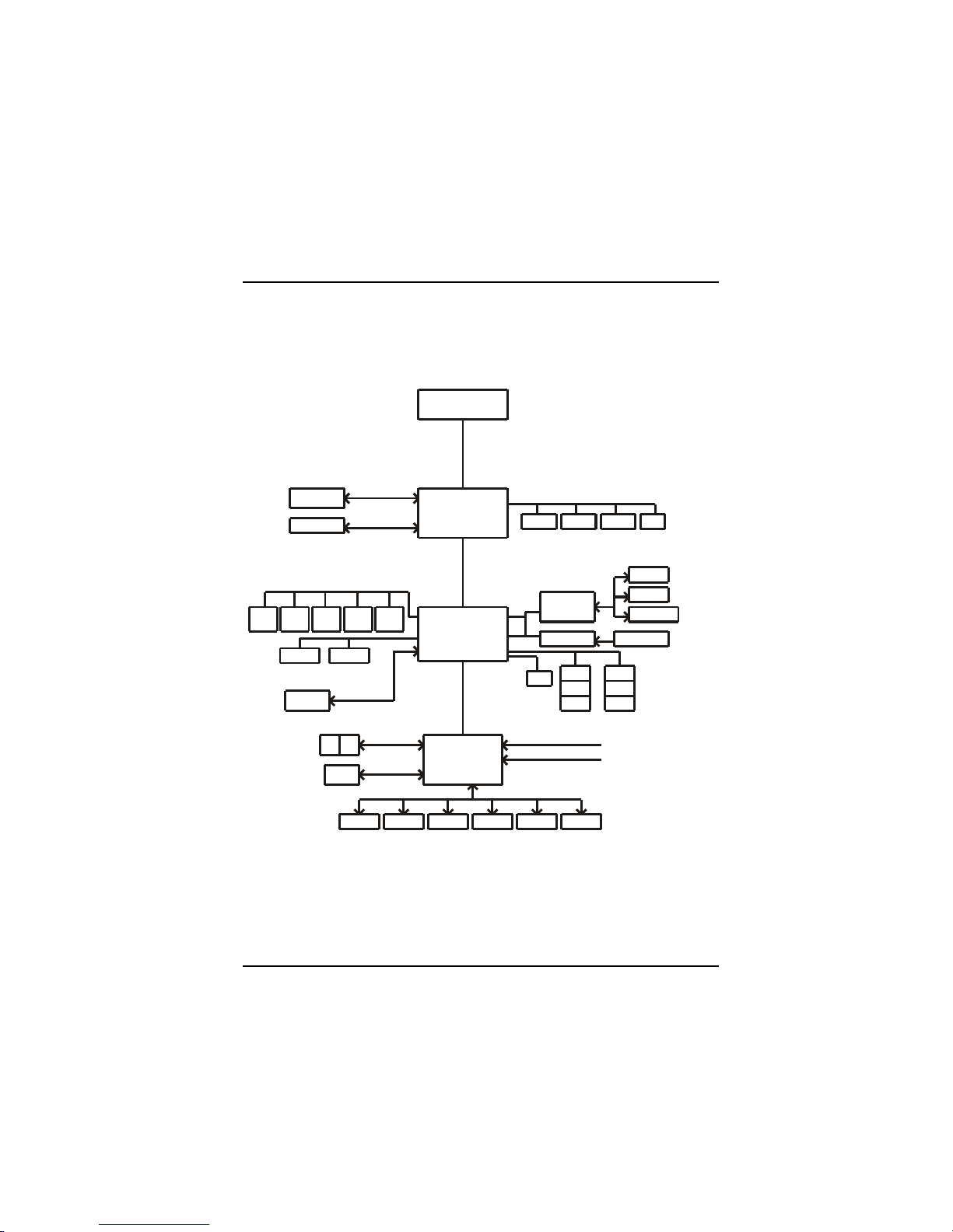
1.2.1 System Block Diagram
M7SXF/H
ATX(FSB: 400MHz)
SUPPORTS 3 DIMMS
SUPPORTS 1 AGP SLOT
SUPPORTS 5 PCI SLOTS
SUPPORTS 1 ACR SLOT
SUPPORTS TELEPHONY
SUPPORTS 1 CNR SLOT
VGA Slot
VGA Connector
PS/2
SOCKET-478
Audio Codec
FAN CONTROL
GAME/MIDI
GPIOs SERIAL PARALLEL FLOPPY
DIMM 1 DIMM 2 DIMM 3
IDE 2
AC'97
USB 0
USB 1
USB 5
Legacy
ROM
PCI
SLOT 3
PCI
SLOT 2
PCI
SLOT 1
USB 3
IR/CIR
FAN1FAN
2
IDE 1
VGA
Analog In
Analog O ut
Rtt
SSTL-2 Termination
(Only for DDR)
ACR
KEYBOARD
/MOUSE
SiS645/650
SiS961
FAN CONTROL
USB 2
USB 4
VOLTAGE MONITOR
TEMPERATURE MONITOR
LPC Supe r I/ O
3D Audi o Out
V-DIMM SLOT
VGA Conn ect or
MII
VGA
512 MB
Support Dual Monitor
Support Max to six-PCI Devices
HyperZip
Host Bus
LPC Bus
DDR SDRAM
PCI
SLOT 4
PCI
SLOT 5
CNR

Chapter 1 Motherboard Description
1-7
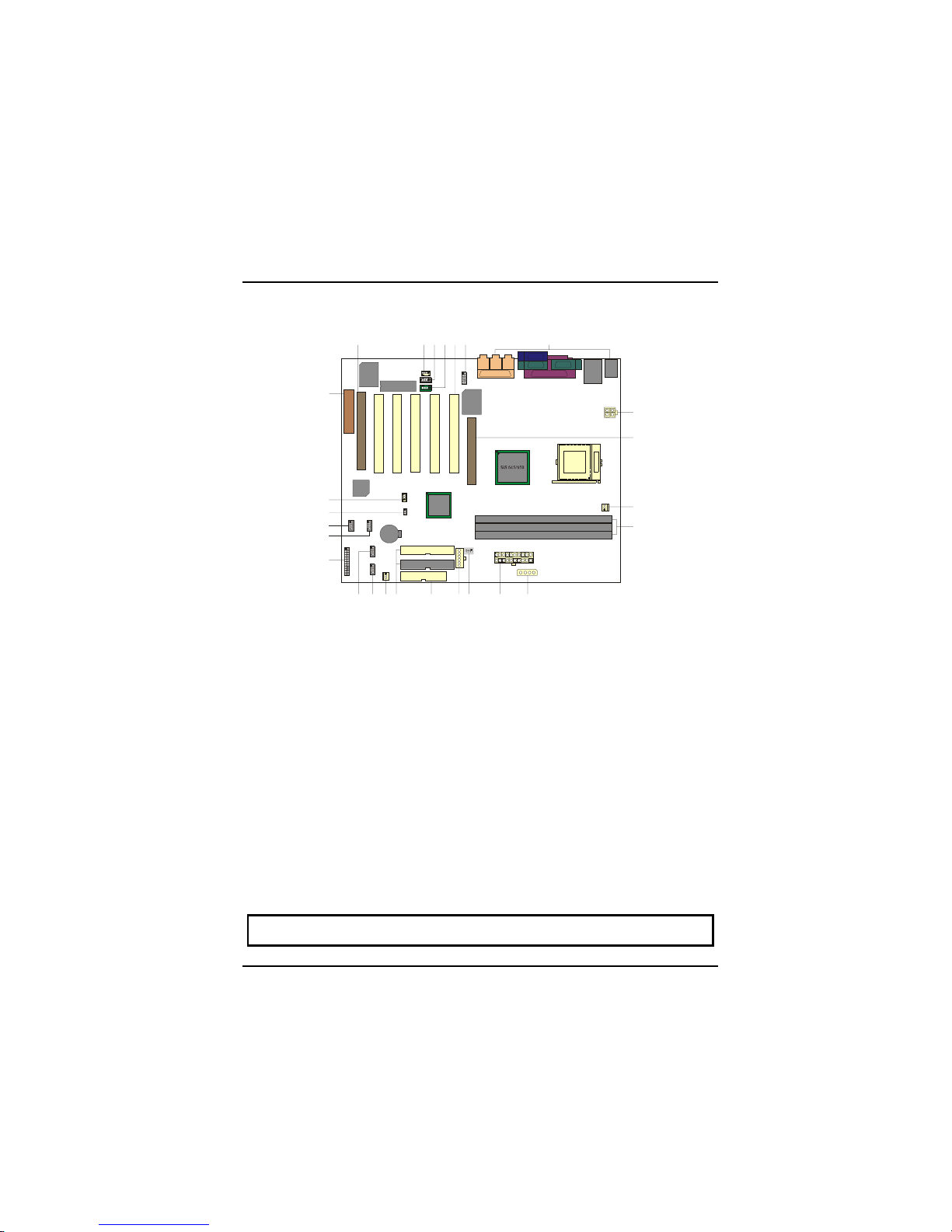
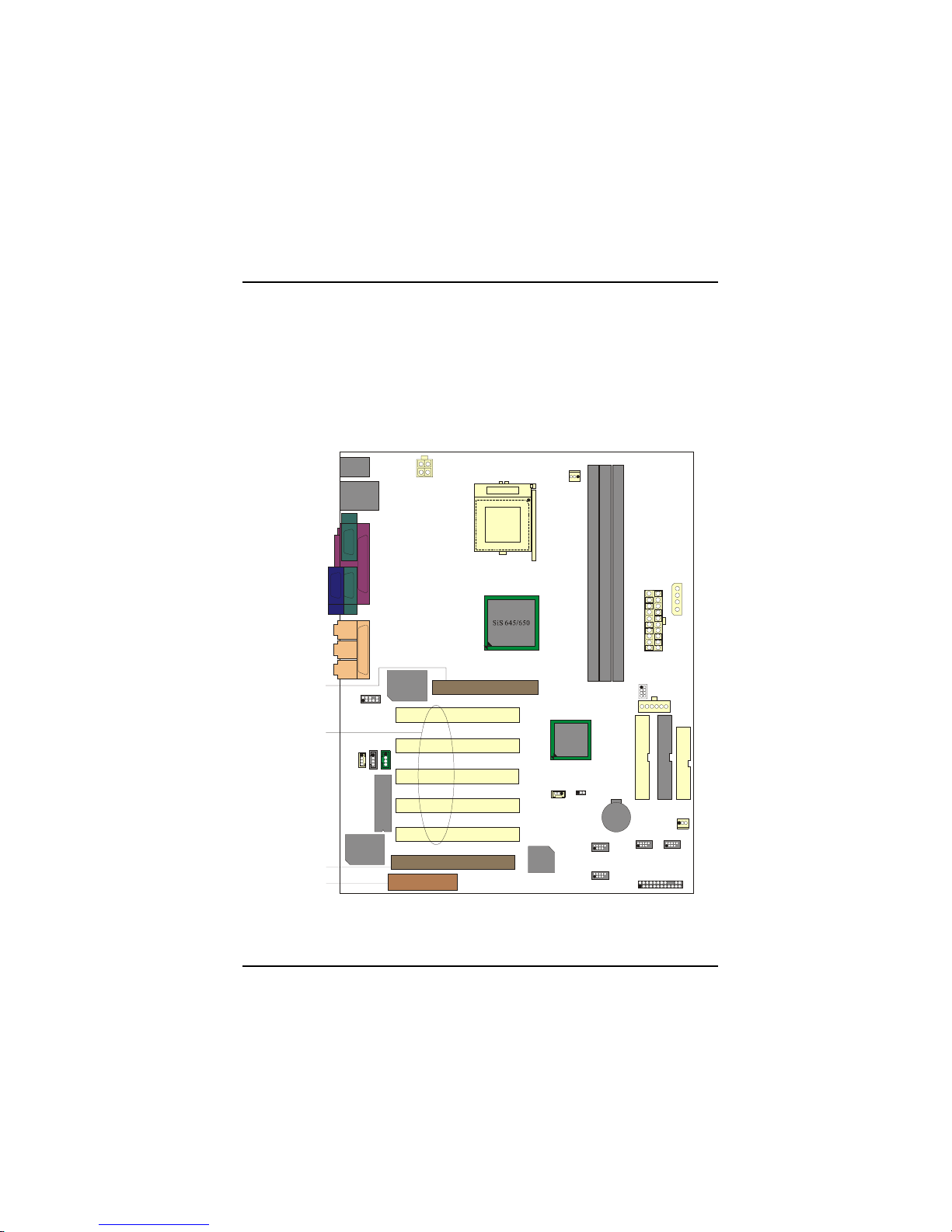
1.2.2 Layout of Motherboard
Model No. M7SXF/H
Notes: When the North Bridge Chipset is 645 (M7SXF), it doesn’t support VGA
onboard, which means there will be JCOM2 on the back panel connectors.
On the contrary, when the North Bridge Chipset is 650 (M7SXH) which
supports VGA onboard, there will be JVGA1 on the back panel connectors.
DDR 1
DDR 2
DDR 3
BIOS
SiS 961
Socket 478
Winbond
I/O
IDE1 IDE2
JSFAN1
1
FDD1
FLOPPY DISK CONN.
SECONDARY IDE CONN.
PRIMARY IDE CONN.
JUSB1
129
10
JAUXPWR2
DDR1 DDR3DDR2
JUSB2
JPANEL1
129
10
12910129
10
2
JWOL1
JCMOS1
BAT1
CNR1
ACR1
PCI5
PCI4
PCI3
PCI2
PCI1
AGP1
JATXPWR1
JAUXPWR1
JATXPWR2
JKBMS1
JCOM1
JPRNT1
JCOM2/JVGA1
JAUD_GAME1
JAUDIO1
JCDIN2
JCDIN1
JTAD1
1
1
1
11
1
1
2
SP-OUT
MIC-IN
LINE-IN
GAME Port
JCFAN1
JDIMMPWR1
LAN
USB
2.0
9109
10
9109
10
121
2
121
2
USB20B1
USB20A1
Chapter 1 Motherboard Description
1-8
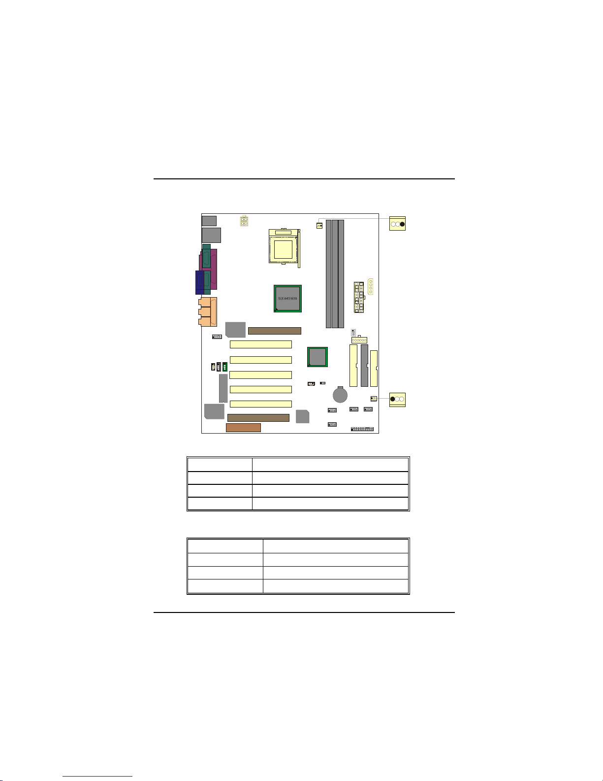
1.2.3 Quick Reference
A. Back Panel I/O Connectors O. Front USB Header (JUSB2)
B. Front Audio Header (JAUDIO1) P. System FAN Header (JSFAN1)
C. PCI BUS Slots (PCI1-5) Q. IDE Connectors (IDE1-2)
D. Telephony Header (JTAD1) R. Floppy Disk Connector (FDD1)
E. CD Audio-In Header (JCDIN1) S. AUX Power Connector (JAUXPWR1)
F. CD Audio-In Header (JCDIN2) T. DIMM Power Voltage Selection Header
G. ACR Slot (ACR1) (JDIMMPWR1)
H. CNR Slot (CNR1) U. ATX Powe r Connector (JATX PW R1)
I. Wake-On-LAN Header (JWOL1) V. AUX Power Connector (JAUXPWR2)
J. Clear CMOS (JCMOS1) W. DDR DIMMs (DDR 1-3)
K. Front USB2.0 Header (*USB20A1) X. CPU FAN Header (JCFAN1)
L. Front USB2.0 Header (*USB20B1) Y. AGP Slot (AGP1)
M. Front Panel Connector (JPAN EL1 ) Z. ATX 12V Power Conne ctor
N. Front USB Header (JUSB1) (JATXPWR2)
NOTE: The “ * “mark mean that the function is optional.
DDR 1
DDR 2
DDR 3
BIOS
SiS 961
Socket478
Winbond
I/O
FLOPPY DISK CONN.
SECONDARY IDE CONN.
PRIMARY IDE CONN.
ABCDEFG
H
I
J
K
L
M
NOPQ R ST U
W
X
V
LAN
USB
2.0
11
11
Y
Z

Chapter 1 Motherboard Description
1-9
1.3 CPU Installation
1.3.1 CPU Installation Procedure: Socket 478
1. Pull the lever sideways away from the socket then raise the lever up to a
90-degre e a ng le.
2. Locate Pin A in th e s o cket and l o ok for t he w hit e dot or cu t edge in the CP U.
Match Pin A with the white dot/cut edge then insert the CPU.
3. Press the lev er down.
4. Put the fan on the CPU by buckling it and then put the fan’s power port into
the JCFAN1, the n the installatio n wi ll be c o m pl eted.
C
P
U
Chapter 1 Motherboard Description
1-10
CPU Installation Layout
1.3.2 CPU Fan Header: JCFAN1
Pin No. Assignment
1
Ground
2
+12V
3
Sense
1.3.3 System Fan Header: JSFAN1
Pin No. Assignment
1
Ground
2
+12V
3
Sense
DDR 1
DDR 2
DDR 3
BIOS
SiS 961
Socket 478
Winbond
I/O
FLOPPY D ISK CON N.
SECONDARY IDE CONN.
PRIMARY ID E CONN.
JCFAN1
1
JSFAN1
1
LAN
USB
2.0

Chapter 1 Motherboard Description
1-11
1.4 RAM Module Installation
1.4.1 DIMM
DRAM Access Time: 2.5V Unbuffered DDR SDRAM (without ECC) PC1600/
PC2100/ PC2700 Type required.
DRAM Type: 128MB/ 256MB/ 512MB/ 1GB DIMM Module (184 pin)
Total Memory Size with unbuffer DIMMs
(Only for reference)
Total Memory
Size (MB)
DIMM 1
DIMM 2
DIMM 3
128 M 128 M ---- ---256 M 256 M ---- ---512 M 512 M ---- ----
1 G 1 G ---- ---256 M 128 M 128 M ---512 M 256 M 256 M ----
1024 M 512 M 512 M ----
2 G 1 G 1 G ---384 M 128 M 128 M 128 M
640 M 256 M 256 M 128 M
1152 M 512 M 512 M 128 M
2.128 G 1 G 1 G 128 M
512 M 128 M 128 M 256 M
768 M 256 M 256 M 256 M
1280 M 512 M 512 M 256 M
2.256 G 1 G 1 G 256 M
768 M 128 M 128 M 512 M
1024 M 256 M 256 M 512 M
1536 M 512 M 512 M 512 M
2.512 G 1 G 1 G 512 M
1.256 G 128 M 128 M 1 G
1.512 G 256 M 256 M 1 G
2.024 G 512 M 512 M 1 G
3 G 1 G 1 G 1 G
Chapter 1 Motherboard Description
1-12
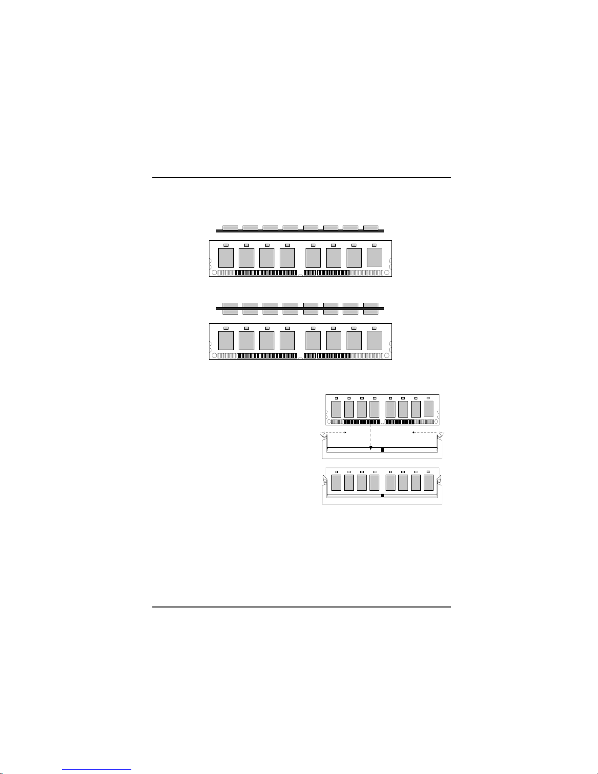
1.4.2 How to install a DIMM Module
1. The DIMM socket has a “ Plastic Safety
Tab” ,and the DIMM memory module has
an Asymmetrical notch”, so the DIMM
memory module can only fit i nto the slot
in one direction.
2. Push the tabs out. Insert the DIMM
memory modules into the socket at a
90-degree angle, then push down vertically
so that it will fit into the place.
3. The Mounting Holes and plastic tabs
should fit over the edge and hold the
DIMM memory modules in place.
Single Sided DIMM
Double Sided DIMM
Chapter 1 Motherboard Description
1-13
1.5 Slots
The slots in this motherboard ar e d esigned to hold expansion cards an d con nect them to
the system bus. Expansion slots are a means of adding or enhancing the motherboard's
features and capabilities. With these efficient facilities, you can increase the
motherboard's capa bilities by adding hardwar e that perfor ms tasks th at are not p art of
the basic system.
DDR 1
DDR 2
DDR 3
BIOS
SiS 961
Socket 478
Winbond
I/O
FLOPPY DISK CONN.
SECONDARY IDE CONN.
PRIMARY IDE CONN.
AGP Slot
PCI Slots
ACR Slot
CNR Slot
LAN
USB
2.0

Chapter 1 Motherboard Description
1-14
1.5.1 ACR (Advanced Com mu n i c ation Ris er) Slot
The ACR specification is an open Industry Standard Architecture and that defines a
hardware scal able riser card inter face, which supports au dio, netw ork and modem
only.
1.5.2 AGP (Accelerated Graphics Port) Slot
Unlike the mouse ports, keyboard ports and printer ports, this motherboard does not
have built in video facilities and therefore requires a video card for one of the
expansion slots. Your monitor will attach directly to that video card. This
motherboard supports video cards for PCI and ISA slots, but it is also equipped
with an Acc elerated Graphics P ort (AGP). An AGP card will take adva ntage of
AGP technology for improved video effici ency and performance, especially with
3D graphics.
1.5.3 CNR (Communication Network Riser) Slot
The CNR specif ication is an op en Industry St andard Architectu re and it defin es a
hardware scal able riser card inter face, which supports au dio, netw ork and modem
only.
1.5.4 PCI (Peripheral Component Interconnect) Slots
This motherboard is equipped with 5 standard PCI slots. PCI stands for Peripher al
Component Interconnect, it is a bus standard for expansion cards, which has
supplanted the older ISA bus standard in most parts. This PCI slot is designat ed as
32 bit.
Chapter 1 Motherboard Description
1-15
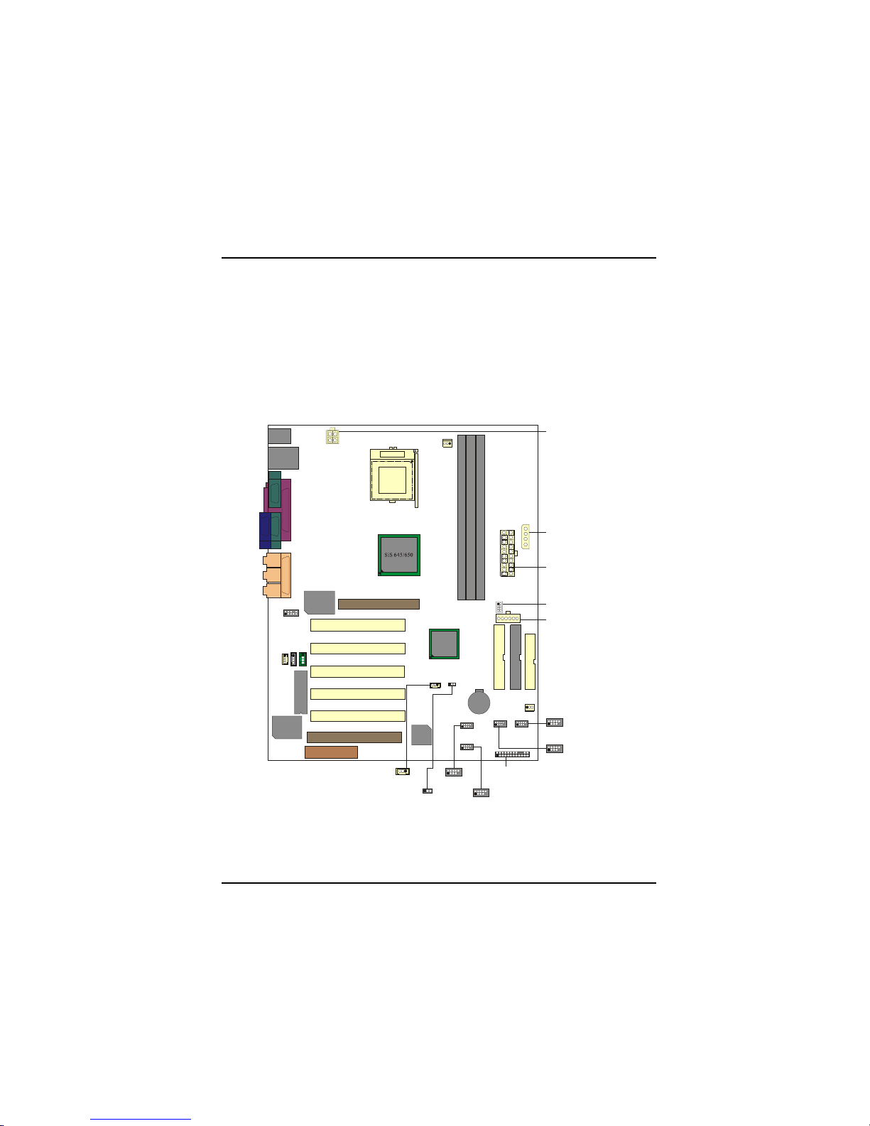
1.6 Connectors, Headers & Jumpers
The connectors, headers and jumpers introduced below provide you lots of
capabilities such as power supply, front panel signal revelation, IDE hard disk
connection, floppy disk connection, Wake On LAN function and USB connection.
Noticeably, a jump er has two or m ore pins that can be cover ed by a plasti c jumper
cap, allowing you to select different system options.
DDR 1
DDR 2
DDR 3
BIOS
SiS 961
Socket 478
Winbond
I/O
FLOPPY DISK CONN.
SECONDARY IDE CONN.
PRIMARY IDE CONN.
JWOL1
JCMOS1
JUSB1
JUSB2
JPANEL1
JAUXPWR1
JDIMMPWR1
JATXPWR1
JAUXPWR2
JATXPWR2
LAN
USB
2.0
USB20A1
USB20B1

Chapter 1 Motherboard Description
1-16
1.6.1 Front Panel Connector: JPANEL1
Pin Assignment Function Pin Assignment Function
No.
No.
1
+5V 2 Sleep Control Sleep
3
NA Speaker 4 Ground Button
5
NA Connector
6
NA
7
Speaker 8 Power LED (+)
9
HDD LED (+) Hard Drive
10
Power LED (+) POWER
11
HDD LED (-) LED
12
Power LED (-) LED
13
Ground Reset 14Power Button Power-on
15
Reset Control Button
16
Ground Button
17
NA 18KEY
19
NA IrDA 20KEY IrDA
21
+5V Connector
22
Ground Connector
23
IRTX
24
IRRX
SPK (Speaker Connector)
An offboard speaker can be installed on the motherboard as a manufacturing option.
An offboard speaker can be connected to the motherboard at the front panel
connector. The speaker (onboard or offboard) provides error beep code information
during the Power On Self-Test when the computer cannot use the video interface.
The speaker is not connected to the audio subsystem and does not receive output
from the audio subsystem.
SPK
POW-LED
ON/OFF
K
E
Y
HLED
IR
SLP
(-)(+)
(-)(+) (+)
N
A
RST
2
1
24
23
NA

Chapter 1 Motherboard Description
1-17
RST (Reset Button)
This connector c an be attached to a m o ment ar y SPST switch. Th is switch is u su all y
open and when closed will cause the motherboard to reset and run the POST
(Power On Self Test).
POW-LED (Power LED Connector)
This connector c an be attached to an LED on the front pan el of a compu ter case.
The LED will illuminate while the comput er is powered on.
HLED (Hard Drive LED Connector)
This connector c an be attached to an LED on the front pan el of a comput er case.
The LED will flic ker during di sk activity. This disk activity on ly applies to thos e
IDE drives directly attached to the system board.
IR (Infrared Connector)
This connector is used to attach to an infrared sensing device. After the IrDA
interface is configured, connectionless data transfer to and from portable devices
such as laptops, PDAs is possible.
SLP (Sleep/Green Button)
This connector is used to conserve energy by powering down the monitor and the
hard disk when not in use. To con figure this option , you need to connect a butt on
from the front panel to this conne ctor. Depressing the button will powe r dow n the
monitor and hard drives until the system is invoked by any keyboard activity,
mouse activity, modem activity or when the sleep button is depressed again.
APM (Advanced P ow er Management) must be enabled in the system BIOS and the
APM driver mus t be lo a de d .
ON/OFF (Power Button)
This connector can be att ach ed to a fron t p anel p ower switch. The swit ch must pu ll
the Power Button pin to ground for at least 50 ms to signal the power supply to
switch on or off . (The time required is du e to internal debounce circuitry on the
system board). At least two seconds must pass before the power supply will
recognize another on/off signal.
 Loading...