

Biostar I915P-A7 Ultra Owner's Manual

I915P- A7 Ult ra
FCC Inf or m at ion and Copyright
This equipment h as been tested and found to comply w ith the limits of a Class
B digi ta l dev i ce, pu r suan t to Part 1 5 of t he FCC Rul e s. Th ese lim it s ar e desig ne d
to provide r easonable protection against harmful interference in a resid ential
installat ion. This equipment generates, uses and can r adiate radio frequ ency
en ergy and, if not installed and used in accordan ce with the instructions, may
caus e harmful interfe rence to radio communications. There is no guarantee
that interferen ce will n ot occur in a particular ins tallation.
The vendor m akes no representations or warranties with respec t to the
con te nt s h ere an d sp e cia ll y di scl a im s a ny im pl i ed w arr ant ie s of mer ch an t abil it y
or fitness for any purpose. Further the ve ndor reserves the right to revise this
publication and to make change s to the contents here wi thout obligation to
notify any party beforehand .
Duplication of this publication, in part or in whole, is not allowed without first
obt ain ing the vendor’s approval in wr iting.
The con te nt of thi s u ser’ s m anu al i s subj ec t to b e ch an ge d w ithou t noti ce an d
we will not b e re sp onsible for any mista kes found in this user’ s manual. All the
brand an d product names are trademarks of their r espective companies.
i

Table of Conte nts
Chapter 1: Introduction ................................................................3
1.1 Motherboard Features.................................................. 3
1.2 Package Checklist......................................................... 7
1.3 Layout and Components...............................................8
Chapter 2: Hardwar e Installation ............................................10
2.1 Central Processing Unit (CPU).....................................10
2.2 FAN Headers..............................................................12
2.3 Memory Module Installation ........................................13
2.4 Connectors and Slots...................................................14
Chapter 3: Heade rs & Jumpers Setup...................................16
3.1 How to Setup Jumpers.................................................16
3.2 Detail Settings.............................................................16
Chapter 4: Useful Help...............................................................22
4.1 Award BIOS Beep Code...............................................22
4.2 Extra Information........................................................22
4.3 Troubleshooting..........................................................24
Chapter 5: WarpSpeeder™.......................................................25
5.1 Introduction................................................................25
5.2 System Requirement....................................................25
5.3 Installation ..................................................................26
5.4 [WarpSpeeder™] includes 1 tray icon and 5 panels........27
ii

I915P- A7 Ult ra
CHAPTER 1: INTRODUCTION
1.1 MOTHERBOARD FEATU RES
A. Hardware
CPU
Supports LGA 775.
Supports single Intel Pentium 4 processor.
Supports Intel Cel eron D processor.
Front Side Bus at the fol lowing frequency ranges:
- 5 33 MT/s (133 MHz Core Clo ck)
- 8 00 MT/s (200 MHz Core Clo ck)
Supports Hyper-Threading Technology.
Chi pset
North Bri dge: Intel 915P.
South Bridge: Intel ICH6.
Dimensions
ATX Form Factor: 24.3cm (W) x 29.35cm (L)
Ma in Memory
Supports DDR333 and DDR400.
Suppo rts 2 56Mb, 512Mb, and 1G-Mb DDR technologies for x8
and x16 non-ECC DDR devic es.
Maximum DRAM address decode space of 4GB.
Registered DIMMs are not supported.
DI MM Socket
Location
DDRA1 128MB/256MB/512MB/1GB *1
DDRA2 128MB/256MB/512MB/1GB *1
DDRB1 128MB/256MB/512MB/1GB *1
DDRB2 128MB/256MB/512MB/1GB *1
DDR Module
3
To t a l Me m or y
Size
Max i s 4G B.

I915P- A7 Ult ra
Slots
Two 32bit PC I bus master slots.
Three PCI-Express x1 slots:
- PCI Express 1.0a com pliant.
- Bandwidth 250MB/s p er dire cti on; 50 0MB/ s total ly.
One PCI-Express x16 slot.
- PCI Express 1.0a com pliant.
- Maximum theoreti cal realized bandwidth of 4GB/s
s imu lta ne ously per dir ecti on, for an ag gr egate of 8GB / s
totall y.
One Xtrem e Graphics Port slot. (See p.14 for detail i nformati on)
Super I/O
Chip: ITE IT8 712.
Low Pin Count Interface.
Provides the most commonly used legacy Super I/O
functionality.
Environment Control initiatives,
- H/W Monitor
- Fan Speed Controller
- IT E's "Smart Guardi an" fu n ction
LAN
Chip: RTL8100C
Supports 10 Mb/s, and 100 Mb/s auto-negotiation.
Half /Full duple x capability.
Supports AC PI power management.
IEEE 1394 Chip (op t i o na l)
Chip: VIA VT6307.
Supports two 1394 Firewire ports with tran sfer up to 400Mb /s.
On-bo ard AC’ 97 Sound Cod ec
Chip: ALC655
Support 6 channels.
Supports S/PDIF-Out and S/PDIF-In (optional) functions.
Compliant with AC’97 Versi on 2.3 specifi cation.
4
I915P- A7 Ult ra
Extend On-b oard IDE
One connector supports 2 IDE di sk drives.
(IDE2/IDE3 are optional.)
Supports PIO Mode 0~4, Bride M ode and Ultra DMA 33/66/100
Bus Master Mode.
ID E Controller ( option al)
Chip: ITE8211 (wi thout RAID functi on)
- Supports two extra slots for 4 IDE devi ces
(IDE2/IDE3).
ITE8212 (with RAID function):
- Supports two extra slots for 4 IDE devi ces
- Integrated RAID 0, RAID 1 and RAID 0+1 for
IDE2/IDE3 slot.
Supports PIO Mode 5, Bride Mode and Ultra DMA
33/ 66/10 0/1 33 Bus Mas t er Mod e.
Se rial ATA
Controller i ntegrated in ICH6.
Supports 4 Serial ATA (SATA) ports.
- Integrated AHCI controller.
- Compliant with Seri al ATA specificati on revision 1.0.
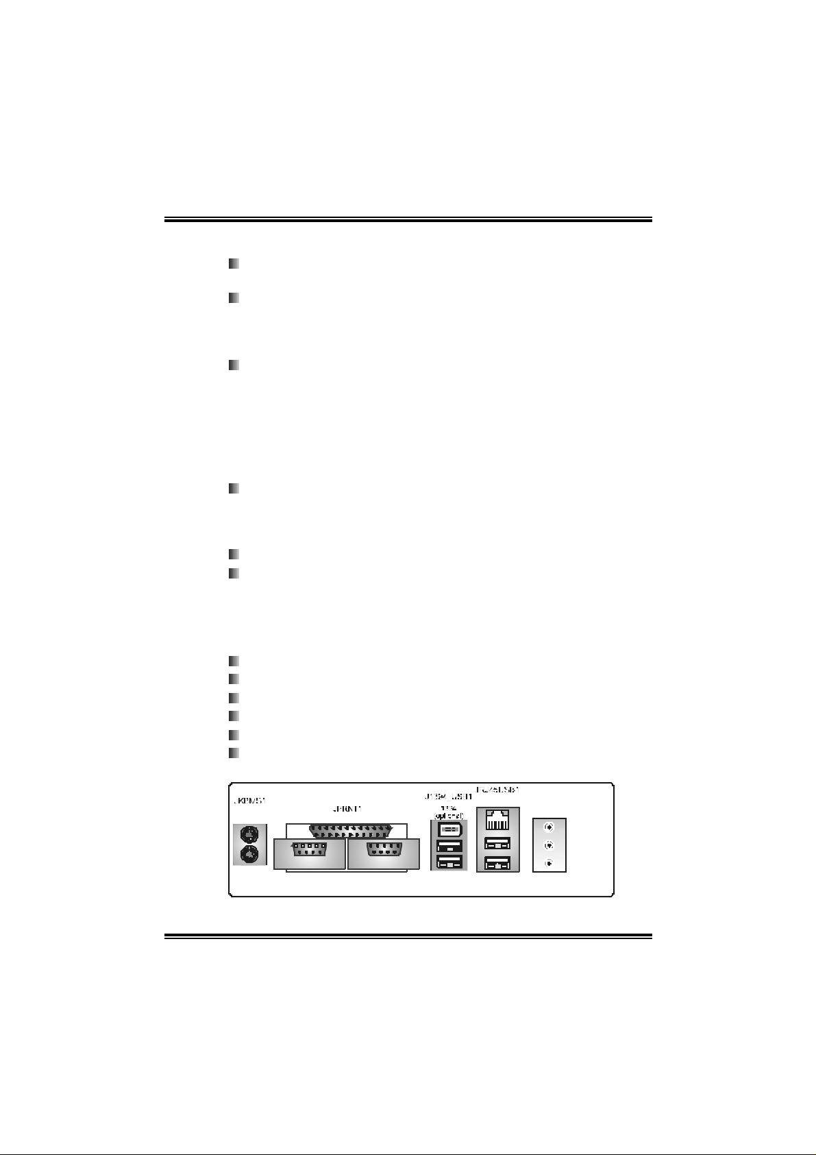
Bac k Panel I / O Connec tor s
4 USB 2.0 ports.
2 serial ports (COM2 i s opti onal).
1 pa r all el po r t.
1 R J- 45 LA N jac k .
1 PS/2 Mouse & Keyboard port.
1 vertical audio port incl udi ng 1 line-in connector, 1 line out
conn ec tor, and 1 MIC in con nector.
PS/2
Mouse
PS/2
Keyboard
COM1
JCOM1
Parallel
COM2
JCOM2
(optional)
LAN
USB x2
5
US B x2
JAUDI O1
Line In/
Surround
Line Out
Mi c In 1/
Base/Center

I915P- A7 Ult ra
I nt er n al On-board I /O Co nn ec tors a nd Headers
1 CD-i n connector supports 1 CD-ROM audio-in device.
1 front panel header supports front panel faciliti es.
1 front audi o header supports front panel audio-out function.
1 S/PDIF-out connector supports digital audio-out function.
1 S/PDIF-in connector supports digital audio-in function
(opti onal ).
1 1394A header supports 1 front panel 1394A Firewire port
(opti onal ).
1 chassis open header supports PC case-opened warning
function.
1 Floppy port supports 2 FDD with 360K, 720K, 1.2M, 1.44M
and 2.88Mbytes.
2 USB headers support 4 USB 2.0 ports.
4 serial ATA connectors support 4 SATA devi ces.
B. BIOS & Software
BIOS
Award legal BIOS.
Supports APM1.2.
Supports ACPI.
Suppo rts USB Functi on.
Software
Supports Warpspeeder™, 9th Touch™, WI NF L A SH ER ™ and
FLASHER™.
Offers the hi ghest performance for Windows 9 8 SE, Windows
2000, Windows Me, Windows XP, SCO UNIX etc.
6

I915P- A7 Ult ra
1.2 PACKAGE CHECKLIST
FDD Cable X 1
HDD Cable X 1
User ’s Manu al X 1
Serial ATA Cable X 1
Fu lly Se tup Dri ver CD X 1
Rear I/O Panel for ATX Case X 1
USB 2.0 Cable X1 (optional)
S/PDIF Cable X 1 (optional )
IEEE 1394 Cable X 1 (optional)
Serial ATA Power Switch Cable X 1 (optional )
7
I915P- A7 Ult ra
(op
)
(
)
(
)
(
)
V
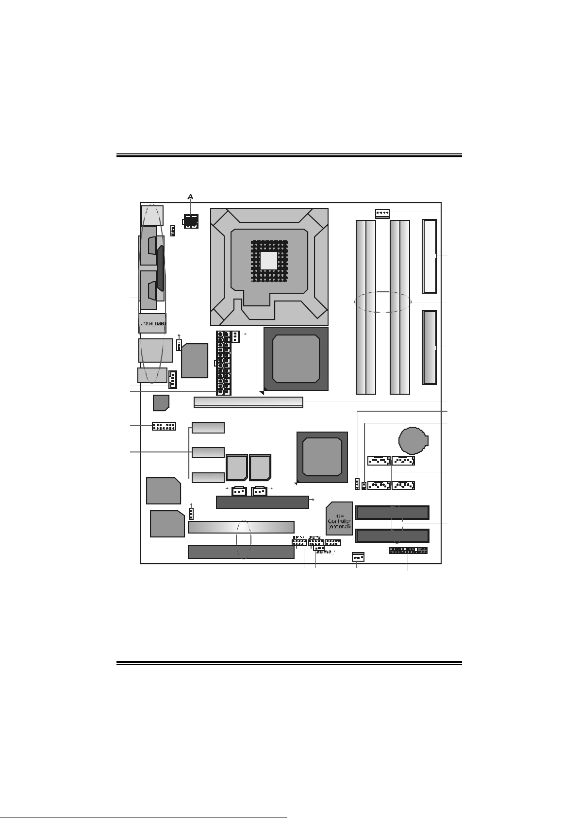
1.3 LAYOUT AND COMPONENTS
B
JK BMS1
JCOM1
C
JCOM 2
(o ptional )
1
JA TXPWR2
JKBV1
C
C
O
O
M
M
1
1
P arallel P ort (JPR NT 1)
LGA775
CPU1
C
O
M
2
JCFAN1
1
DDRA1
DDRB1
D DRA2
D DRB2
U
FDD1
T
JUSBV1
Super
I/O
PCI-Ex1_ 1
PCI-Ex1_ 2
PCI-Ex1_ 3
JSPDI F_IN1(optional)
JATXP WR1
YZ
W
Codec
JA UDIOF1
1213
1
1
JCDIN1
14
JRJ45USB1
JAUDI O1
D
E
F
G
LAN
A1
J139 4PWR1
(op tional )
Chip
tional
1
PCI1
IEEE 1394
H
PCI2
Note: ■ represents the 1st pin.
X
1
JSFAN2
( optional )
PCI EXPRESS x16
BIOS
BIOS
optional
XGP 1
11
JS PDIF _OUT1
Intel
915P
Intel
SAT A4
ICH6
SA TA1
1
1
JCMOS1
A2
J1 394A1( optional )
1
1
1
1
IJ K L M
JCL1
IDE3
IDE2
JSFAN1
optional
optional
1
S
IDE1
R
Q
P
BAT1
SA TA3
1
1
77
SATA2
17
1
7
O
N
JPANEL1
2
1
24
23
8

I915P- A7 Ult ra
JATXPW R 2: ATX power source header.
A.
JKBV1: Pow er source header for JKBMS1.
B.
Back panel (rear s ide) I/O connec t ors .
C.
JCDIN1: CD-ROM audio-in connec tor.
D.
JATXPW R 1: ATX power source header.
E.
JAU DIOF 1: F ront panel audio-out header.
F.
PCI -Ex 1_1~PC I -Ex1_3: PCI EXPRESS x1 slots.
G.
PCI 1/ PCI2: Peripheral C om ponent Interconnect slot s.
H.
JU SB3/JU SB4: H eaders for U SB 2.0 port at front panel.
I.
JU SBV3_1: Power sourc e f or JUSB3/JUSB4.
J.
J1394A1: Header f or 1394 F irewire port at front panel (opt ional).
K.
JSFAN1 : Power source header for s ystem fan.
L.
JPAN EL1: Front panel f acilit ies header.
M.
ID E2/ID E3: H ard dis k device c onnectors (optional).
N.
SATA1~SATA4: On-board s erial ATA c onnectors.
O.
JC L1: Chassis open m es s age header.
P.
JCM OS1: Clear CMOS header.
Q.
PCI -Ex 16: PC I EXPRESS x 16 slot .
R.
ID E1: Hard disk dev ic e connec t or.
S.
DDRA1~D DRB2: DD R memory m odules.
T.
FDD1: Floppy disk dev ic e connec t or.
U.
JCFAN 1: Power sourc e header f or CPU fan.
V.
JU SBV1: Power sourc e header f or J1394_U SB1 and JR J 45U SB1.
W.
JSFAN2 : Power source header for s ystem fan (optional).
X.
JSPD IF_IN1: Digital audio-in c onnec t or (optional).
Y.
JSPD OF _OUT1: D igit al audio-out connector.
Z.
J1394PW R 1: Power s ourc e header f or 1394 Firewire port (optional).
A1.
XGP1: Xt rem e Graphic Port s lot.
A2.
9
I915P- A7 Ult ra
soc
ket to ensu re p in le g s wo n
t be damag e d.
CHAPTER 2: HARDWARE INSTALLATION
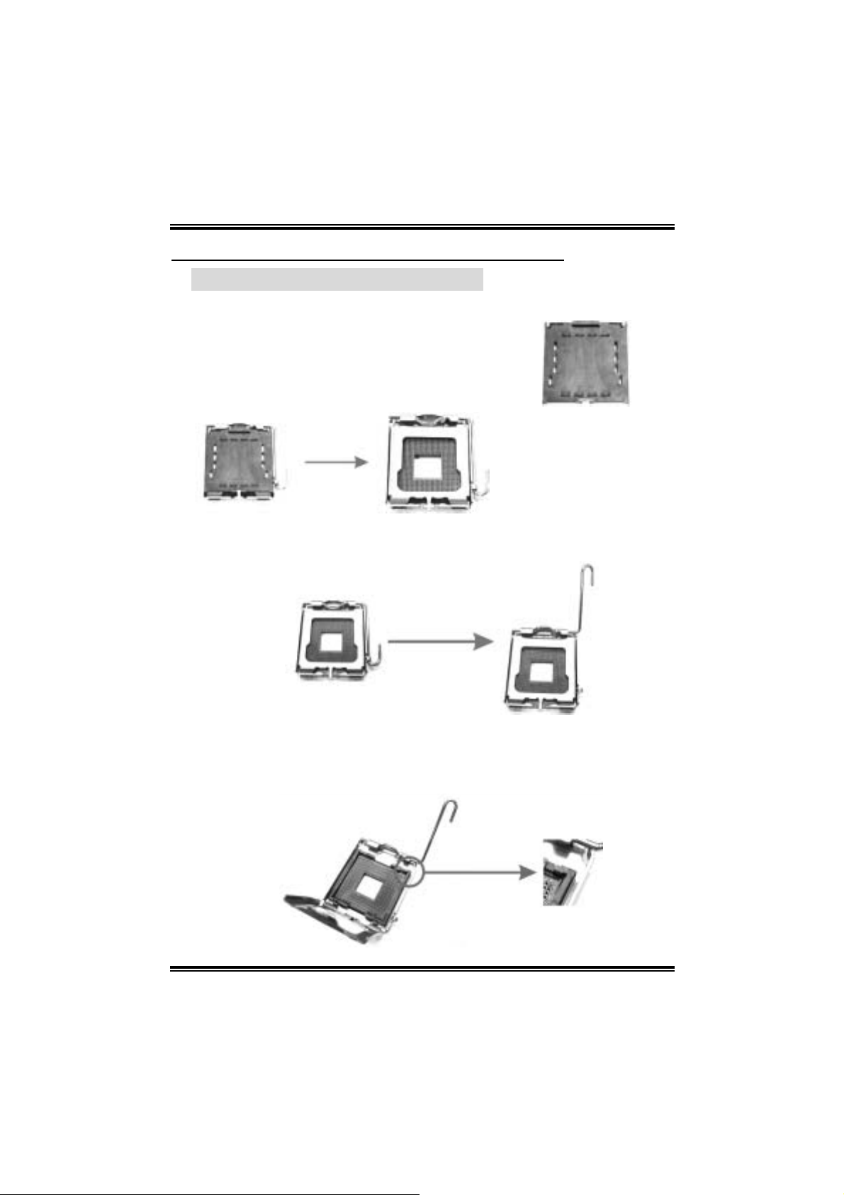
2.1 CENTRAL PROCESSING UNIT (CPU)
Special Notice:
Remo v e Pin Cap before installatio n, and m ake
good preservation for future use. When the CPU
is remov e d, cover the Pin Cap on the empty
’
Step 1: Pull the lever sideways away from the socket and then raise the
lever up to a 90-degree angl e.
Pin Cap
Step 2: Look for the black cut edge on socket, and the white dot on CPU
should point wards this black cut edge. The CPU will fit o nly in the
correct orientation.
Step 2-1:
10
I915P- A7 Ult ra
Step 2-2:
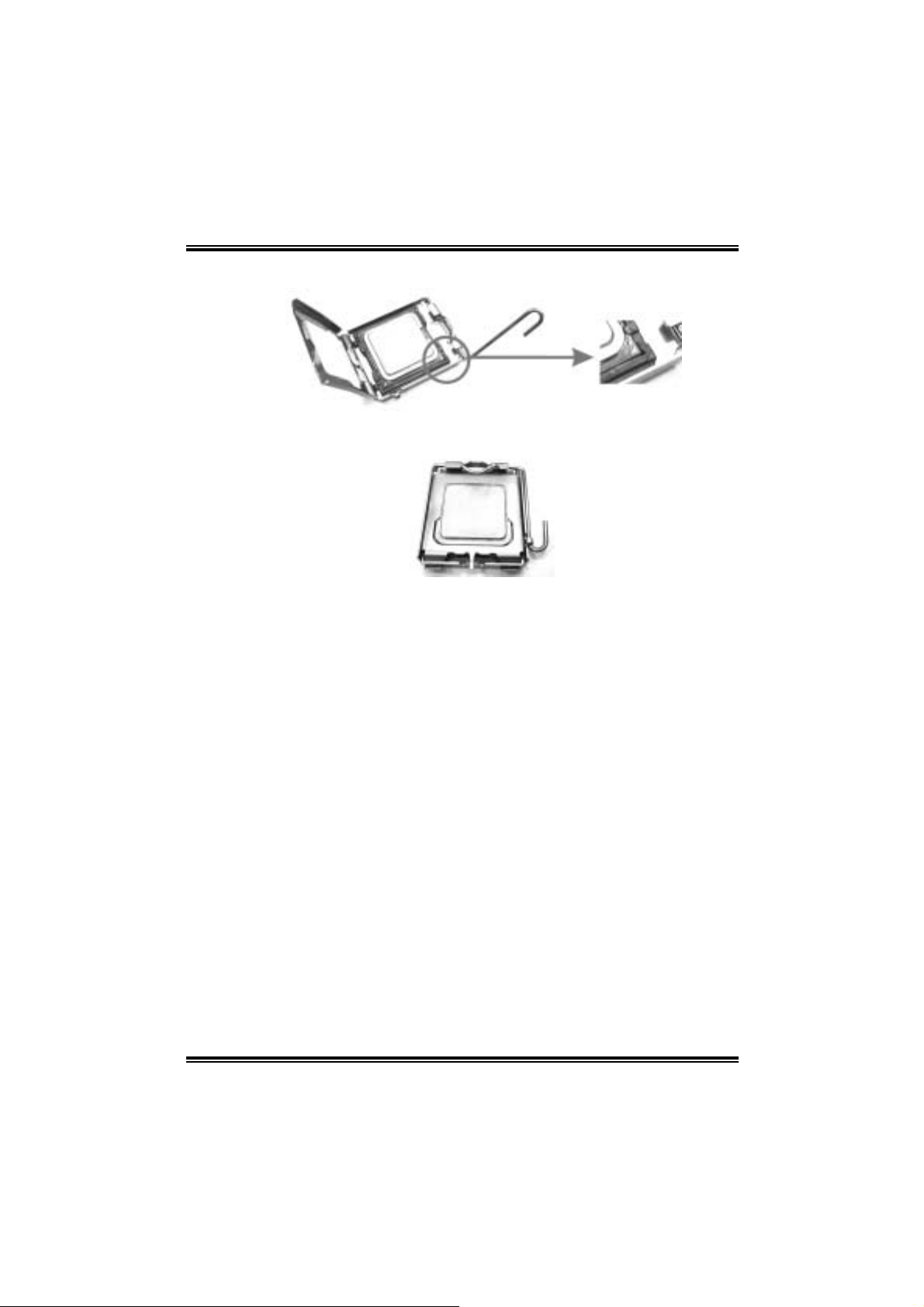
Step 3: Hold the CPU down firml y, and then close the lever to complete
the i nstalla ti on.
Step 4: Put the CPU Fan on the CPU and buckle it. Connect the CPU FAN
power cable to the JCFAN1. This completes the i nstallation.
11
I915P- A7 Ult ra
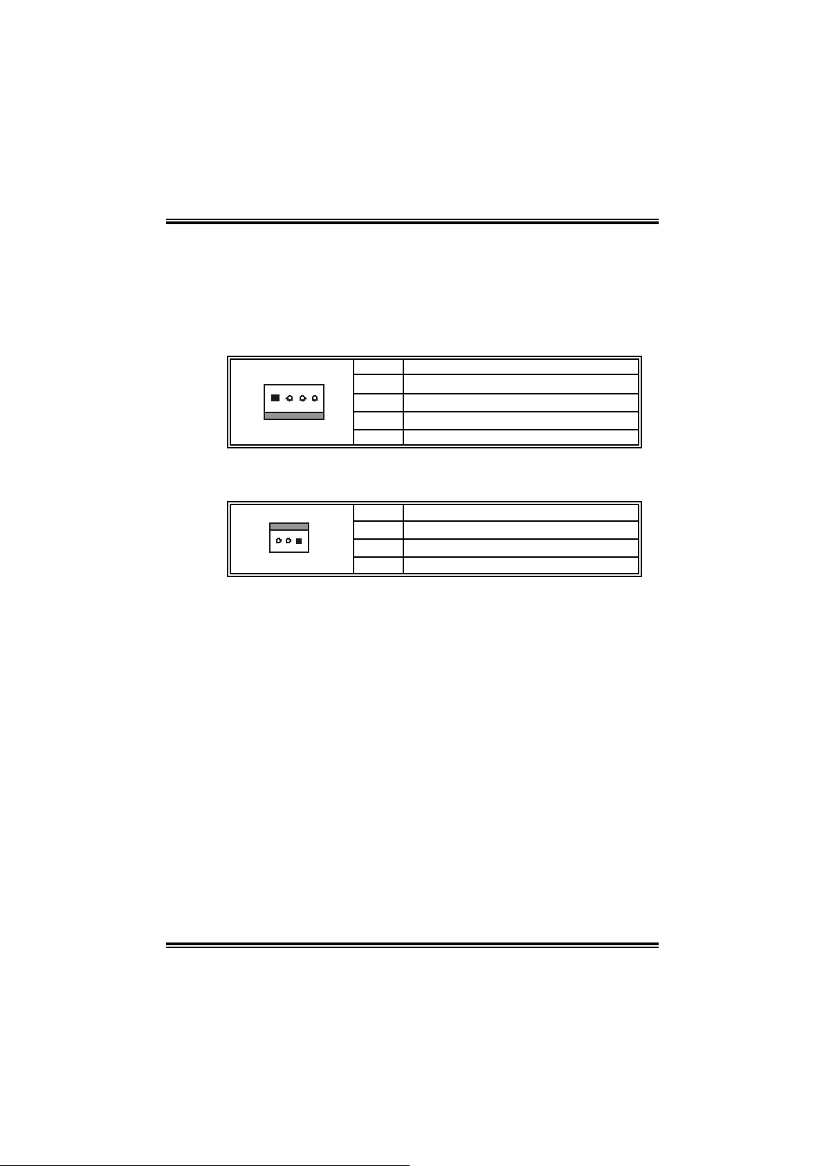
2.2 FAN HEADERS
These fan headers support cooling-fans bui lt in the com puter. T he fan
wir in g and plu g may be dif f er ent accordi ng to the f a n ma nufactur er.
Connect the fan cable to the connector while m atching the bl ack wire to
pin#1.
JCFAN1: P ower Source for CPU F a n
Pin Assignment
1 Ground
1
JSF AN1/ JSFAN2: P ower Source for System F an
(JSFAN2 is optional.)
1
Note:
The JCFAN1 and JSFAN1support system cooling fan wi th Smart Fan
Control utili ty. It supports 3-pin and 4-pin head connectors. When
connecting with wires onto connectors, please note that the red wire is
the positi ve and should be connected to pin#2, and the black wire i s
Ground and should be connected to GND.
2 Power
3 FAN RPM rate sense
4 Smart Fan Control
Pin Assignment
1 Ground
2 Smart Fan Control
3 FAN RPM rate sense
12
I915P- A7 Ult ra
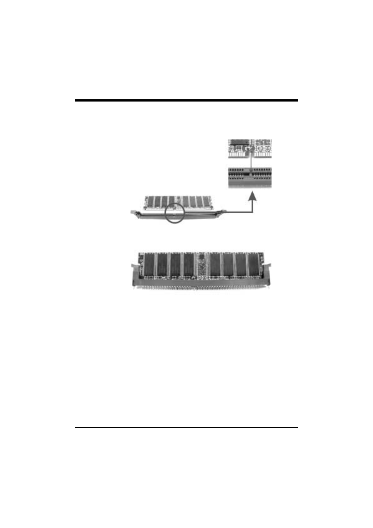
2.3 MEMORY MODUL E INSTALLATION
1. Unlock a DIMM sl ot by pressing the retaining clips outward. Align a
DIMM on the slot such that the notch on the DIMM m atches the break
on the Sl ot.
2. Insert the DIM M vertically and firm ly into th e slot until the re tain ing chip
snap back in place and the DIMM i s properly seated.
13

I915P- A7 Ult ra
2.4 CONNECTO RS AND SLOTS
FDD1: Floppy Disk Connector
The m otherboard provides a standard fl oppy disk connector that supports
360 K, 720K, 1.2 M, 1.44M and 2.8 8 M floppy d is k ty pes. Th is c onn ec tor
supports the provided floppy drive ribbon cables.
IDE1/IDE2/IDE3 : Hard Disk Connectors
(IDE2/IDE3 are optional.)
The m otherboard has a 32-bit Enhanced PCI IDE Controller that provides
PIO M ode 0~5, Bus Master, and Ultra DMA 33/ 66/ 100 functionality. It has
two HDD co nn ectors IDE1 (primary) an d IDE2 (seconda ry ).
The IDE connectors can connect a master and a sl ave drive, so you can
connect up to four hard disk drives. The first hard drive should al ways be
connected to IDE1.
PCI 1/PCI2: Peripheral Component Interconnect Slots
This motherboard is equi pped with 2 standard PCI slots. PCI stands for
Per i ph er al C o mp onent Interc on nect, an d it is a bus stand ar d f or exp ansion
cards. Thi s PCI slot i s desig nated a s 32 bits.
Xtreme Graphics Port Slot: XGP1
This XGP (Xtreme Graphi cs Port) slot i s a special desi gn that only
supports compatible AGP VGA cards.
To install the system with an add-on AGP VGA card, please make sure
to install the driver of add-on AGP VGA card before onboard VGA dri ver
installation. If the onboard VGA dri ver has already been installed before
you install the add-on AGP VGA card, the system will automati cally set
the onboard VGA as the pri mary graphi cs adapter.
For the onboard VGA driver can’t be removed com pletely, and to sol ve
this problem, please follow the steps bel ow,
1. Disable onboard VGA utility under the operating system, and reboot
PC. After PC restarts, the system will automati cally set the AGP
VGA card as the graphi cs adapter. Or,
2. Re-install your operating system to ensure the AGP VGA card
function c an be used.
Note:
Please go to “http: //www. biosta r.com.tw” for more detailed information
abou t XGP compatible AGP cards.
14
I915P- A7 Ult ra
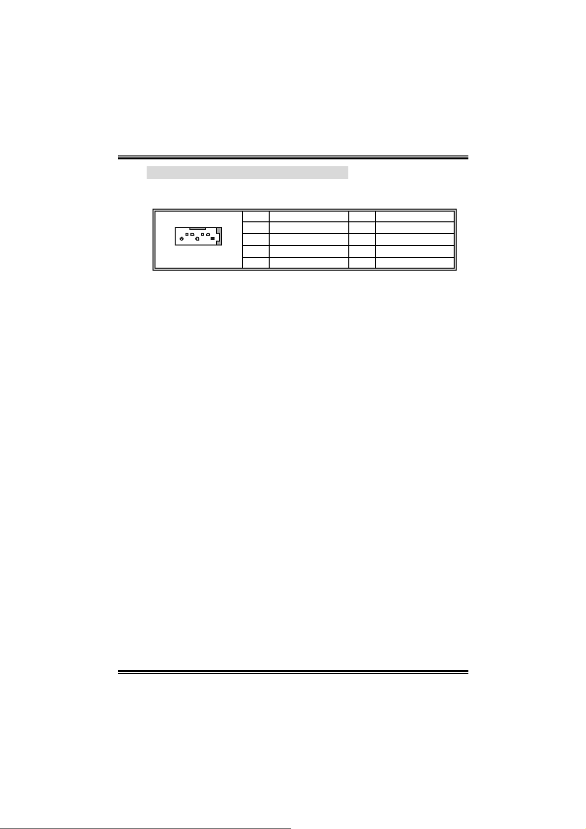
SATA1~SATA4: Serial ATA Connectors
The m otherboard has a PCI to SATA Control ler with 2 channels SATA
interface, it satisfies the SATA 1.0 spec and with transfer rate of 1.5Gb/s.
Pin Assignment Pin Assignment
1 Ground 2 TX+
17
3 TX- 4 Ground
5 RX- 6 RX+
7 Ground
15
I915P- A7 Ult ra
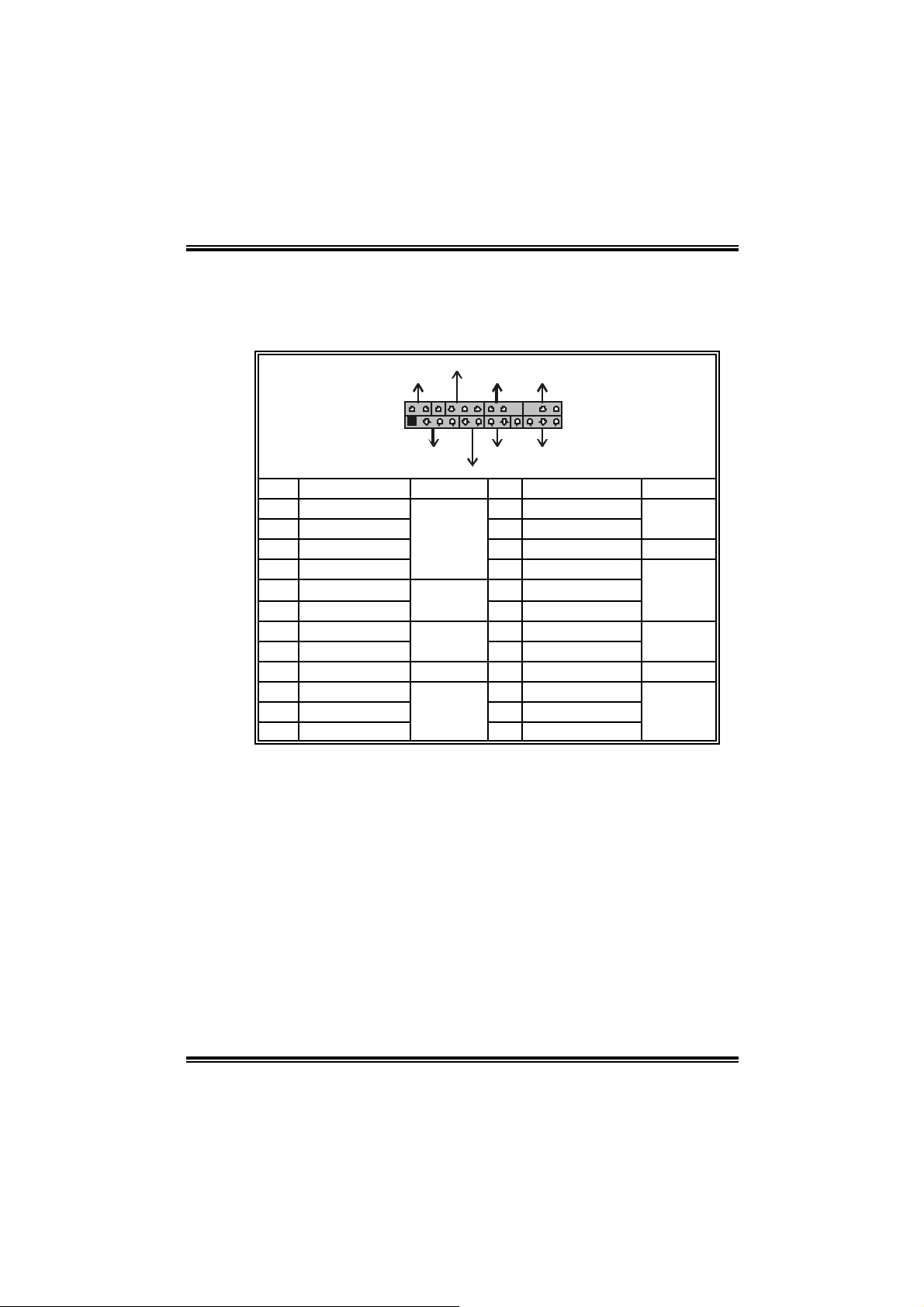
CHAPTER 3: HEADERS & JUMPERS SETUP
3.1 HOW TO SETUP JUMPE RS
The illustration shows how to set up jumpers. When the jumper cap is
placed on pins, the jumper is “cl ose”, if not, that means the jumper is
“open”.
Pin opened Pin closed Pin1-2 closed
3.2 DETAIL SETTINGS
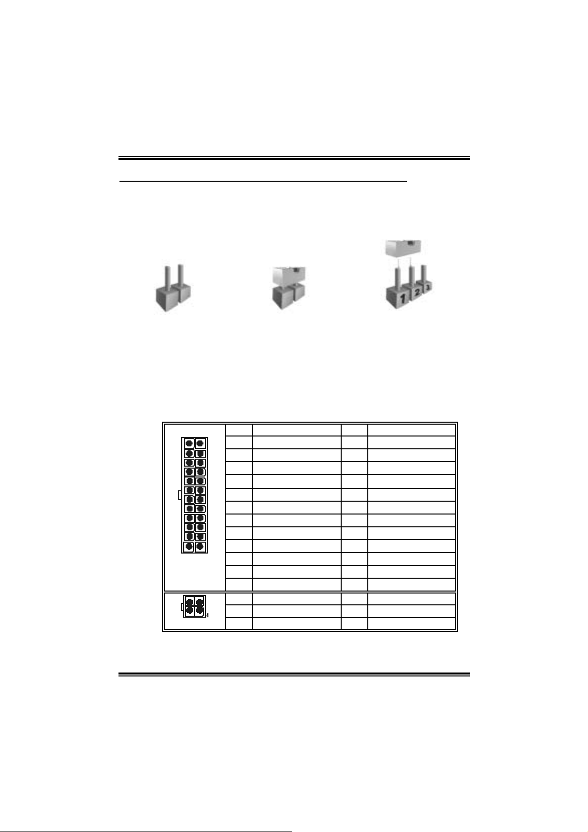
Power Conn ect ors: JAT X PWR1/ JATXPWR2
JATXPWR1: This connector allows user to connect 20-pi n power
conn ec tor on t h e A T X pow er supp ly .
JATXPWR2: By connecting this connector, i t will provide +12V to CPU
power ci rcuit.
Pin Assignment Pin Assignment
13
24
JATXPWR1
JATXPWR2
1
1 +3.3V 13 +3.3V
2 +3.3V 14 -12V
3 Ground 15 Ground
4 +5V 16 PS_ON
5 Ground 17 Ground
6 +5V 18 Ground
7 Ground 19 Ground
8 PW_ON 20 -5V
9 Standby Voltage +5V 21 +5V
12
10 +12V 22 +5V
11 +12V 23 +5V
12 2 x 12 Det ect 24 Ground
1
3
Pin Assignment Pin Assignment
2
1 +12V 3 Ground
2 +12v 4 Ground
16
I915P- A7 Ult ra
V
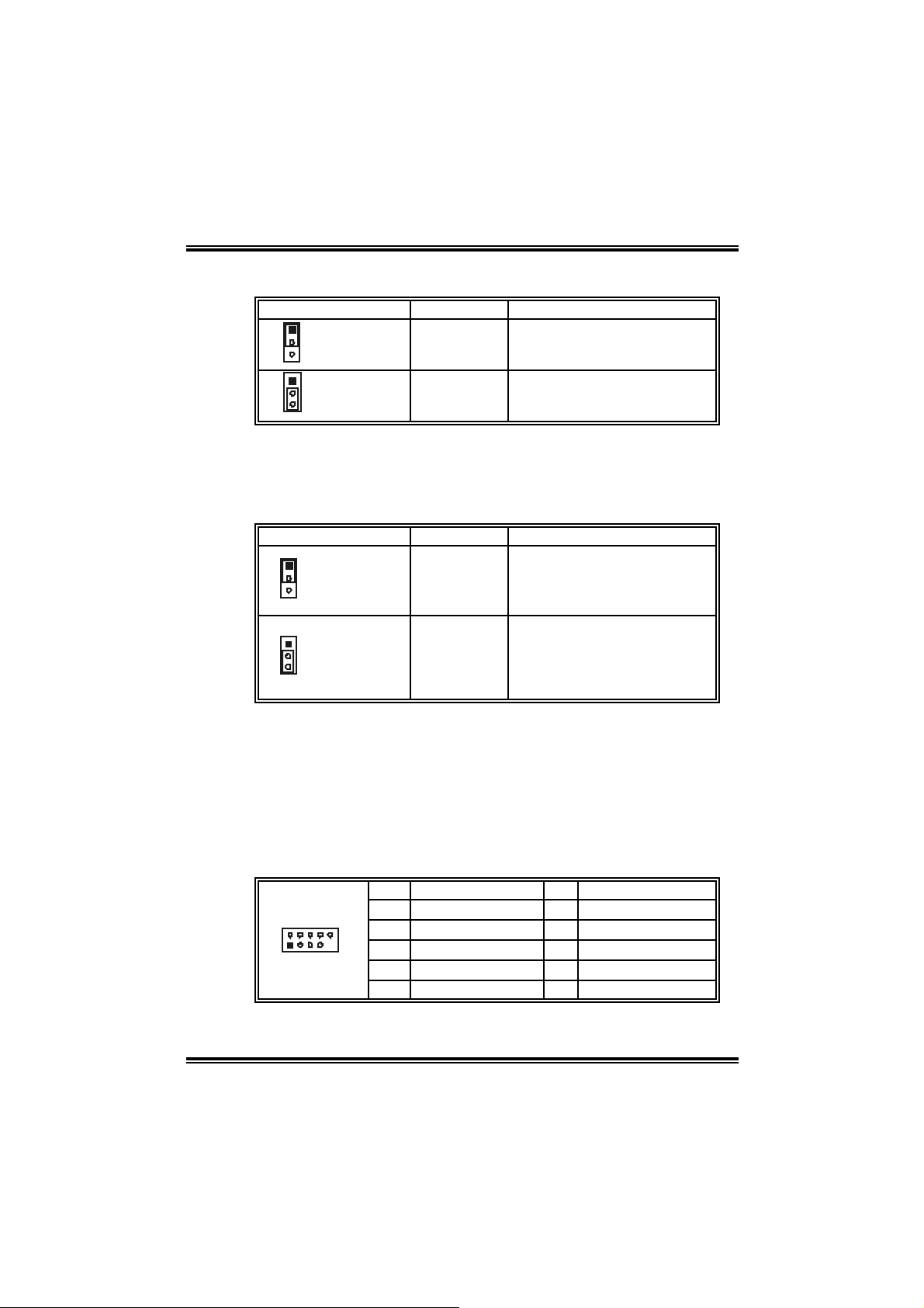
JKBV1: Power Source Heade r for PS/2 Keyboard an d Mouse
Assignment Description
1
3
Pin 1-2 close
1
3
Pin 2-3 close
+5V
+5V Standby
Voltage
+5V for PS/2 ke yboard and
mouse
PS/2 m ouse and k ey board are
powered wit h +5V standby
voltage.
Note:
In order to support thi s function “Power-on system via keyboard and
mouse”, “JKBV1” jum per cap should b e placed on Pi n 2-3.
JUSB V1/JUS BV 3_1: Power Sour ce H eade r for US B Ports
Assignment Description
1
3
Pin 1-2 close
1
3
Pin 2-3 close
+5V
+5V st andby
Voltage
Note:
In order to support thi s function “Power-o system via USB devi ce,”
“JUSBV1/ JUSBV3_1” jumper cap should be placed on Pin 2-3
individually.
JUSBV1: + 5V for JUSB_19341
and JRJ45U SB1.
JU SBV3_1: +5V for
JUSB3/JUSB4.
JU SBV1: JUSB_19341 and
JRJ45U SB1 are powered by +5
standby v oltage.
JU SBV3_1: JUSB3/JUSB4 are
powered by +5V.
JUSB3/JUSB4: Headers for USB 2.0 Ports at Front Panel
This header allows user to connect addi tional USB cable on the PC
front panel , and al so can be connected with internal USB devices, like
USB card reader.
Pin Assignment Pin Assignment
1 +5V (fus ed) 2 +5V (fus ed)
2
1
3 USB- 4 USB-
10
5 USB+ 6 USB+
7 Ground 8 Ground
9 Key 10 NC
17
I915P- A7 Ult ra
JCDIN1: CD-R OM A ud io-i n Connector
This connector allows user to connect the audio source from the
va riety devi ces, like CD-ROM, DVD-ROM, PCI so und card , PCI TV
turner card etc..
Pin Assignment
1
1 Left channel input
2 Ground
3 Ground
4 Right channel input
JAUDIOF1: Front P anel Audio-out Header
This header allows user to connect the front audio out put cable with
the PC front panel. It will disable the ou tput on back panel audio
connectors.
2
1
Pin Assignment Pin Assignment
1 Mic in/center 2 Ground
3 Mic power/Bass 4 Audio power
Right line out/ Speak er out
5
Right
7 Reserved 8 Key
9 Left line out/ Speak er out Lef t 10 Left line out/ Speak er out Lef t
Right line in/R ear s peak er
11
Right
13 Left line in/R ear s peak er Lef t 14 Left line in/R ear speaker Lef t
14
13
Right line out/ Speak er out
6
Right
Right line in/R ear s peak er
12
Right
JSPDIF_IN1: Digital Audio-in Connector (optional)
This connector allows user to connect the PCI bracket SPDIF i nput
header.
Pin Assignment
1
1 +5V
2 SPDIF_IN
3 Ground
18
I915P- A7 Ult ra
JSP DIF_OUT1: Digital Audio-out C onn e ctor
This connector allows user to connect the PCI bracket SPDIF output
header.
Pin Assignment
1
1 +5V
2 SPDIF_OUT
3 Ground
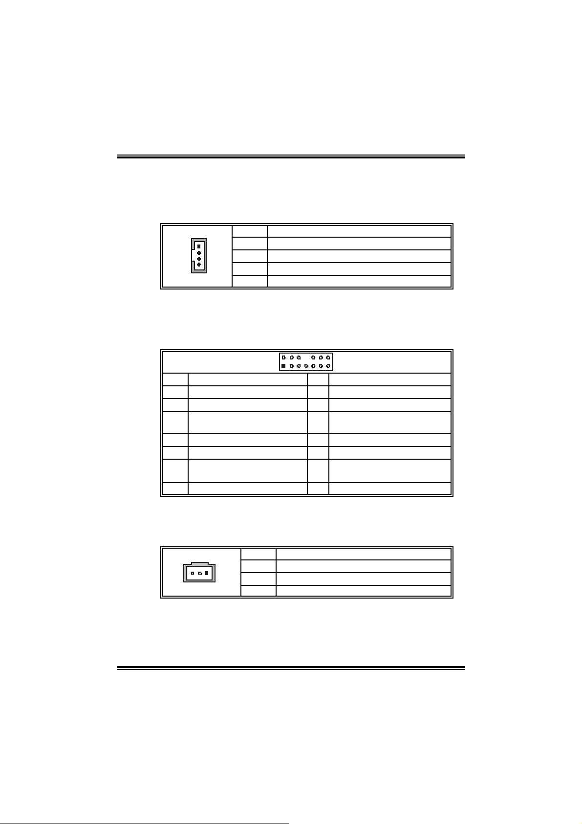
J1394PWR1: Powe r Source for 1394 Firewi re Port (optional )
This header allows user to connect the digital image device, l i ke DV,
D8, or V8 , etc.
1
3
Pin 1-2 close
1
3
Pin 2-3 close
Assignment Description
+3.3V SB +3.3V SB f or 1394 chips et.
+3.3V
+3.3V for 1394 chipse t.
(Default)
J1394A1: Header for 1394 Firewi re Port at Front Panel (optional)
Pin Assignment Pin Assignment
1 A+ 2 A-
2
1
10
3 Ground 4 Ground
5 B+ 6 B7 +12v 8 +12V
9 Key 10 Ground
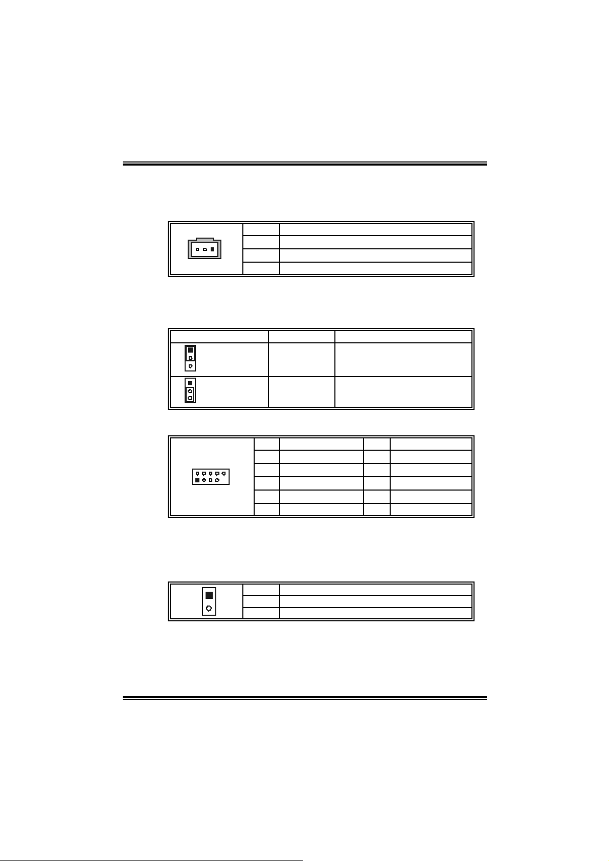
JCL1: Chassis Open Messag e Header
T his connector allows system to monitor PC case open sta tu s. If the
signal has been triggered, i t will record to the CMOS and show the
message on next boot-up.
1
Pin
1 C as e open signal
2 Ground
19
Assignment
I915P- A7 Ult ra
JCMOS 1 : C lear CMOS H eader
By pl aci ng the jumper on pin2-3, i t allows user to restore the BIOS
safe setting and the CMOS data, please carefully follow the
pr oced ur es to av o id da ma g ing th e mot her b oar d .
1
3
Pin 1-2 close
1
3
Pin 2-3 close
Norm al Operation (D ef ault).
Clear CMOS data.
Assignment
※ Clear CMOS Procedures:
1. Remov e AC power line.
2. Set the jumper to “Pin 2-3 cl ose”.
3. W ait for five seconds.
4. Set the jumper to “Pin 1-2 cl ose”.
5. Powers on the AC.
6. Reset your desired password or clear the CMOS data.
20
I915P- A7 Ult ra
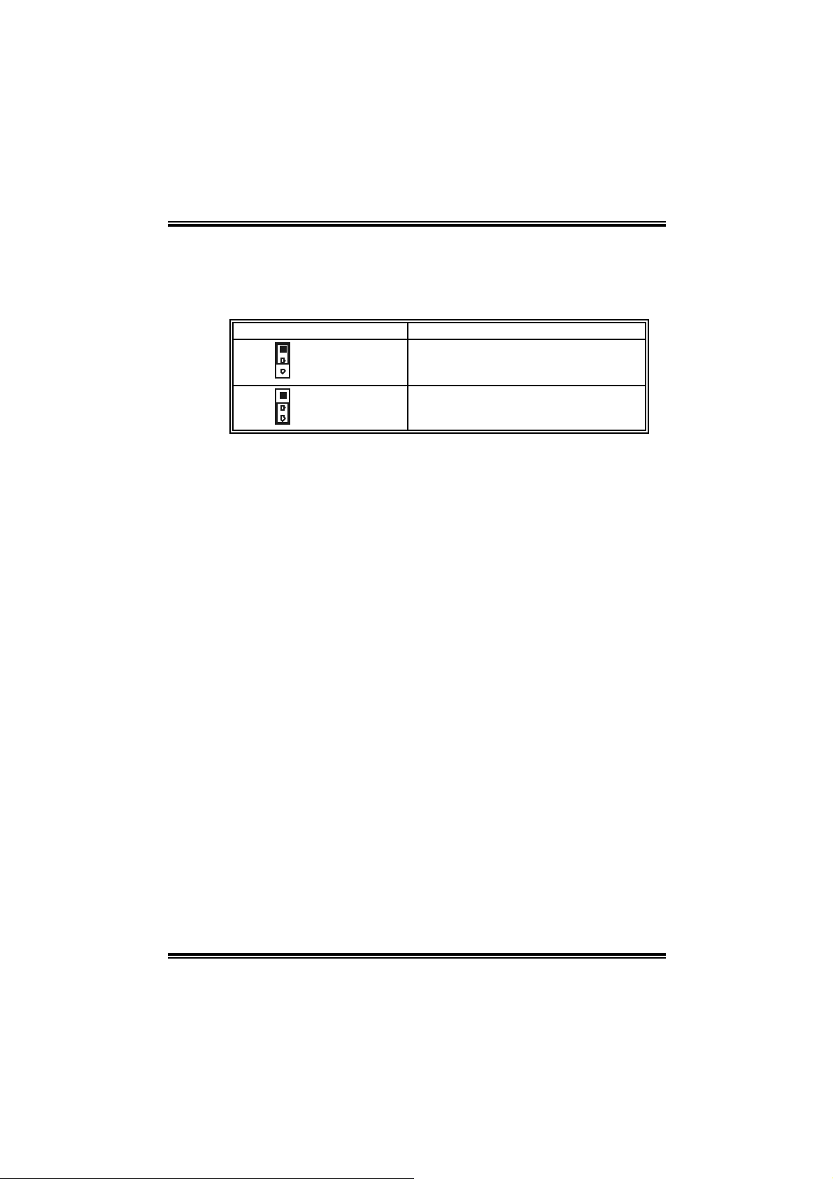
F r ont Pa n el Conn ect or : JPA NEL 1
This 24-pin conne c tor in cl udes Po wer-on, Reset, HDD LE D, Power
LED, Sleep button, speaker and IrDA Connection. It allows user to
connect the PC case’s front panel switch functions.
PWR_LED
SLP
2
1
SPK
On/Off
++
+--
RST
HLED
Pin Assignment Function Pin Assignment Function
1 +5V 2 Sleep control
3 N/A 4 Ground
5 N/A 6 N/A N/A
Speaker
Connector
7 Speaker
9 HDD LED (+) 10 Power LED (+)
11 HDD LED (-)
13 Ground 14 Power button
15 Reset control
Hard drive
LED
Reset
button
17 N/A 18 Key
19 N/A 20 Key
21 +5V 22 Ground
IrDA
Connector
23 IRTX
IR
24
23
IR
8 Power LED (+)
12 Power LED (-)
16 Ground
24 IRRX
Sleep
button
Power LED
Power-on
button
IrDA
Connector
21
 Loading...