

Page 1

GeForce 6100-M9
FCC Inf or m at ion and Copyright
This equipment h as been tested an d fou n d to comply with the limits of a Class
B digi ta l dev i ce, pu r su ant to Part 15 of t he F CC Rul e s. Th ese lim it s ar e de sig ned
to provide reasonable protection against harmful interference in a residential
installat ion. This equipment generates, use s and can radiate radio f requency
en ergy and, if not i nstalled and used in accor dance with the in structions, may
caus e harmful interfe rence to radio communications. There is no guarantee
that interference will not occur in a particular installation.
The vendor makes no representations or warranties with respec t to the
con te nt s h ere an d sp ec iall y di scl a im s an y imp li ed w arran t ies of mer c ha nt ab il ity
or fitness for any purpose . Furt he r t he vendor reserves the right to revise this
publication and to make changes to the con tents here w ithout obligation t o
notify any party beforehand .
Duplication of this publication, in part or in whole, is not allowed without first
obt aining t h e vendor’s approval in writing.
The con te nt of thi s u ser’s m anu al is subje ct to b e ch ange d with ou t no tic e an d
we will not be responsible for any mistakes found in this user’ s manua l. All the
brand an d product names are trademarks of their r espect ive c ompanie s.
i
Page 2

Table of C onte nt s
Chapter 1: Introduction.......................................................................1
1.1 Motherboard Features.......................................................... 1
1.2 Layout and Components.......................................................4
Chapter 2: Hardware Installation...................................................5
2.1 Installing Cen tral Processin g Unit (CPU)................................5
2.2 FAN Headers....................................................................... 6
2.3 Installing Sy stem Mem ory .................................................... 7
2.4 Connectors and Slots............................................................ 9
Chapter 3: Headers & Jumpers Setup........................................11
3.1 How to Setup Jumpers.........................................................11
3.2 Detail Settings.....................................................................11
Chapter 4: Useful Help ..................................................................17
4.1 Award BIOS Beep Code.......................................................17
4.2 Extra Information................................................................17
4.3 Troubleshooting..................................................................19
Chapter 5: WarpSpeeder™..............................................................20
5.1 Introduction........................................................................20
5.2 System Requirement............................................................20
5.3 Installation ..........................................................................21
5.4 [WarpSpeeder™] includes 1 tray icon and 5 panels................22
ii
Page 3

GeForce 6100-M9
CHAPTER 1: INTRODUCTION
1.1 MOTHERBOARD FEATURES
CPU
Supports Socket 939.
Sup por ts AMD At h l on 64 FX/ Athlon 64/ At hl on 64 X 2 proces sor.
AMD 64 architecture enabl es sim ultaneous 32 and 64 bi t
computing.
Sup por ts Hy perTransport Technol ogy up to 20 00MT/s.
Sup por ts AMD Co ol’n’Quiet T echn ology.
Chi pset
Nor th Br idge: nVIDIA GeFor ce 61 00.
South Bridge: nVIDIA nForce 410.
Dimensions
Micro ATX Form Factor: 24.5cm (L) x 24.45cm (W)
Op erating System Supp orting
Supports Windows 2000 and Windows XP.
Note: Does not support Window s 98SE and Window s ME.
Slot
Two PCI bus master sl ots.
One PCI-E x1 sl o t.
One PCI-E x16 sl ot.
Super I/O
Chip: ITE IT8712F.
Low Pin Count Interface.
Provides the most commonly used legacy Super I/O
functionality.
Environment Control initiatives,
H/W Monitor
F an Sp eed Con tr oller
ITE's " Smart Guardian" function
1
Page 4
GeForce 6100-M9
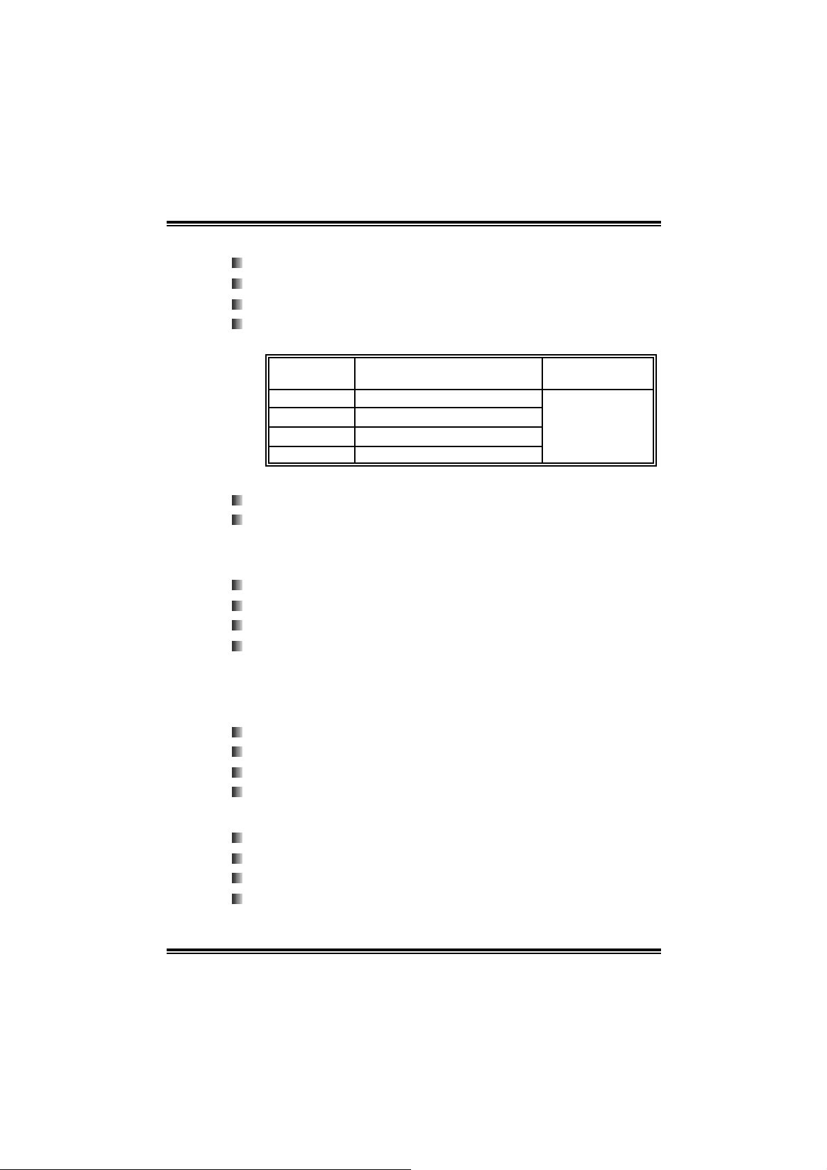
S ystem Memory
Supports Dual Channel DDR..
Supports 8 banks in total.
Supports DDR-266/333/400.
Maximum memory size i s up to 4GB. (Following tabl e is only for
reference.)
DI MM Socket
Location
DIMMA1 128MB/256MB/512MB/1GB *1
DIMMA2 128MB/256MB/512MB/1GB *1
DIMMB1 128MB/256MB/512MB/1GB *1
DIMMB2 128MB/256MB/512MB/1GB *1
On-board IDE
Two on-board connectors support 4 IDE disk drives.
Supports PIO mode 0~4, Block Mode and Ultra DMA
33/ 66/ 100/1 33 bus m aster mode.
Onb oard Ser ial ATA
Integrated in nForce 410.
Four serial ATA connectors support 2 SATA devi ces.
Supports RAID 0 and RAID 1 functions.
Supports 2 serial ATA (SATA) ports.
- Data tran sfer rates up to 3.0 GB/s.
- Compliant with SATA Version 2.0 specifi cation.
DDR Module Total Memory Size
Max is 4 GB.
10 /100 LAN PHY
PHY: RTL8201BL/RTL8201CL.
Supports 10 Mb/s and 100 Mb/s auto-negotiation.
Half/Full duplex capability.
Supports ACPI, PCI power management.
Onb oard AC’97 Sound Cod ec
Chip: ALC655
Support 6 channels.
Supports S/PDIF o u t function.
Compliant with AC’97 Versi on 2.3 specification.
2
Page 5
GeForce 6100-M9
I nt er n al On-board I/O Con n ec tors and H eader s
1 front panel header supports front panel faciliti es.
1 CD-i n connector supports 1 CD-ROM audio-in device.
1 front audi o header supports front panel audio function.
1 S/PDIF-Out connector supports di gital audi o-out function.
1 chassis open header supports PC case-opened warning
function.
1 FDD connector supports 2 Fl oppy drives with 360K, 720K,
1.2 M, 1.44M and 2.88Mby tes.
2 IDE connectors support 4 hard disk devices.
2 Serial ATA connectors support 2 SATA devices.
2 USB headers support 4 USB 2.0 ports at front panel.
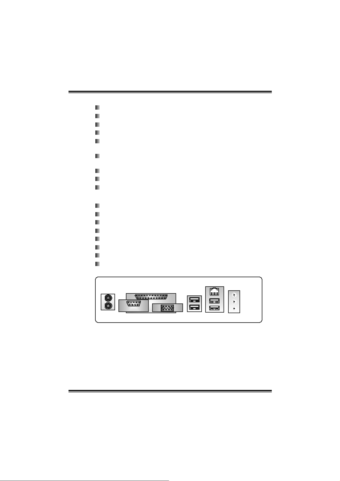
Back Panel I/ O Connec tors
4 USB 2.0 ports.
1 VGA port.
1 Serial port.
1 Printer port.
1 RJ - 45 LAN jack.
1 PS/2 Mouse port.
1 PS/2 Keyboard port.
1 Vertical audio port including 1 Line-in connector, 1 Line-out
conn ec tor, and 1 MIC - in co nn ec tor.
PS/2
Mouse
PS/2
Keyboard
C
O
COM1
LAN
Par al le l
1
M
VGA1
U SB x2
US B x 2
L ine In/
Surround
L ine Out
Mic In 1/
Bass/Center
3
Page 6
GeForce 6100-M9
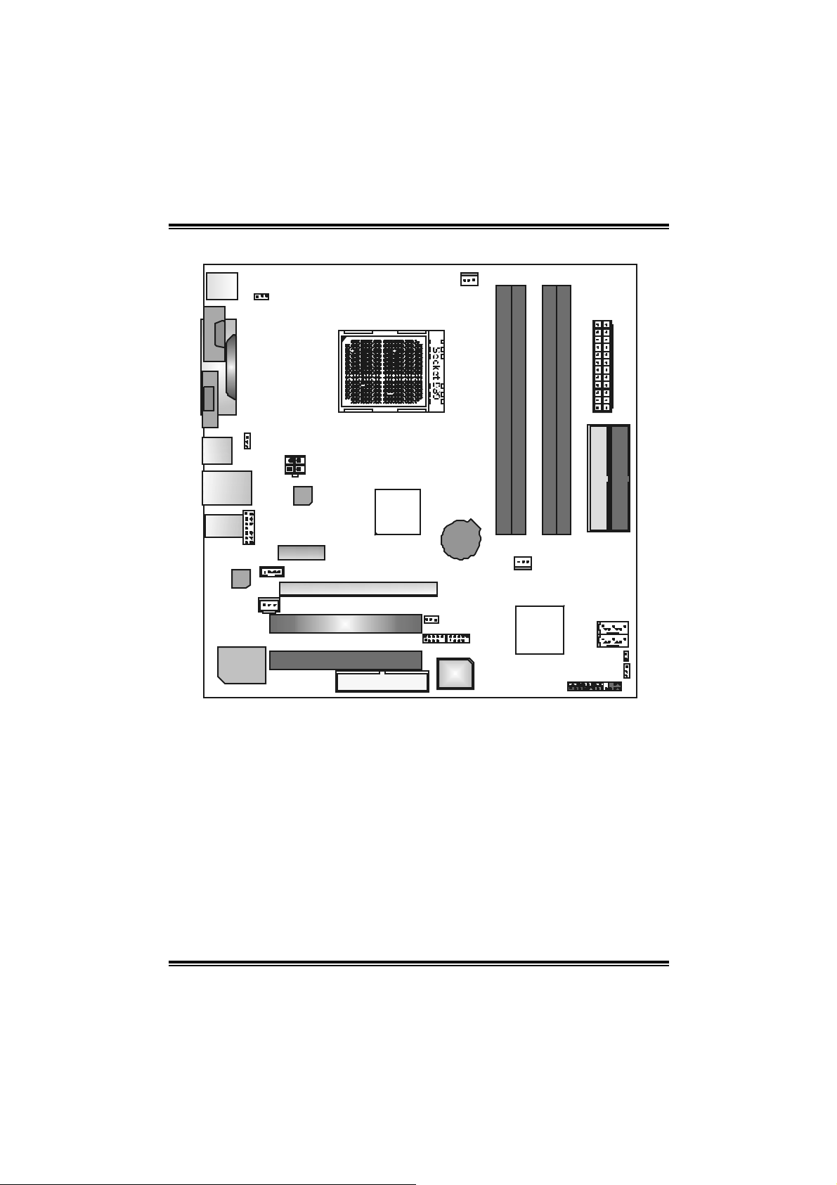
1.2 LAYOUT A ND COMPONE NTS
J KBMS1
JKBV1
JCFAN1
JCOM1
JVGA1
JUSB1
JUSBLAN1
J AUDIO 1
JPRN T1
JU SB V1
JAT XPW R2
JAUDIO2
PCI-EX1_1
JC DI N1
Codec
JSPDIF_OUT1
Super I/O
LAN
PHY
CPU 1
PCI-EX16
PCI1
PCI2
GeForce
6100
FDD1
Note: ■ represents the 1st pin.
JUSB V2
JUSB 2 JU SB3
BAT1
BIOS
DIMM B1
DIMMB2
JSFAN1
nForce
410
JATXPWR1
DIMMA1
DIMMA2
ID E2
IDE1
JS ATA2
JS ATA1
JCI1
JC M O S1
JPANEL1
4
Page 7
GeForce 6100-M9
CHAPTER 2: HARDWARE INST ALL ATION
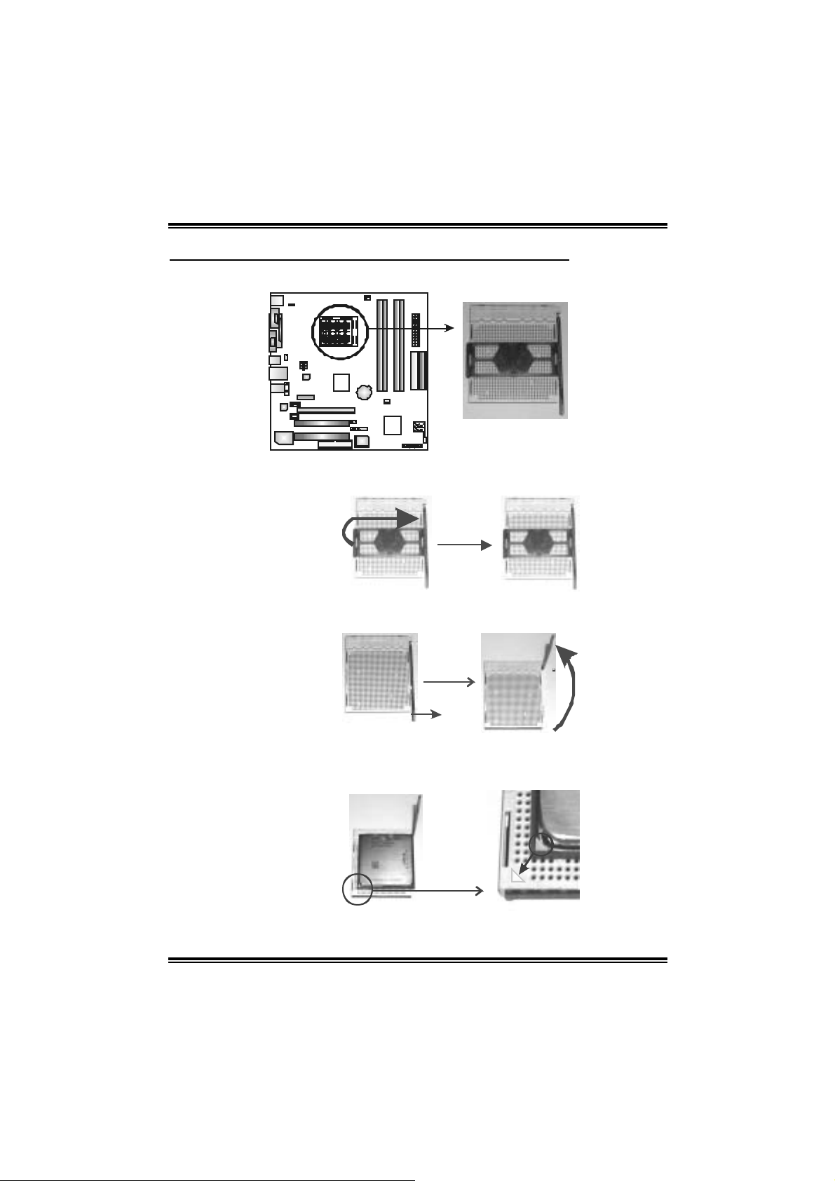
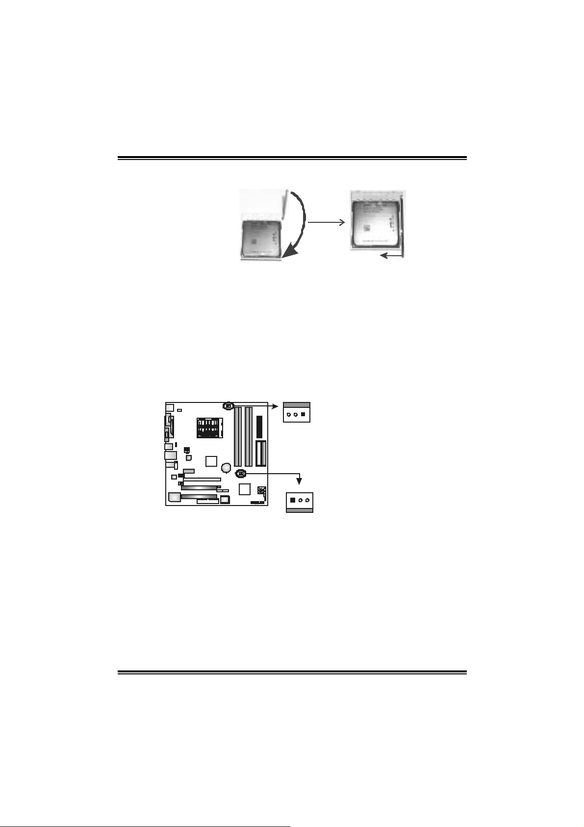
2.1 INSTALL ING CENTRAL PROCESSING UNIT (CPU)
Step 1: Remove the socket protection cap.
Step 2: Pull the l ever toward direction A from the socket and then raise the
lever up to a 90-degree angl e.
90
A
Step 3: Look for the white triangle on socket, and the gold triangle on
CPU should point forwards this white triangle. T he CPU will fit
on ly in the corr ec t or i entat io n.
5
Page 8
GeForce 6100-M9
Step 4: Hold the CPU down firml y, and then close the lever toward di rect
B to complete the insta ll atio n.
B
Step 5: Put the CPU F an on t he CP U and bu c kl e it. Connec t the CPU
FAN power cable to the JCFAN1. This completes the i nstallation.
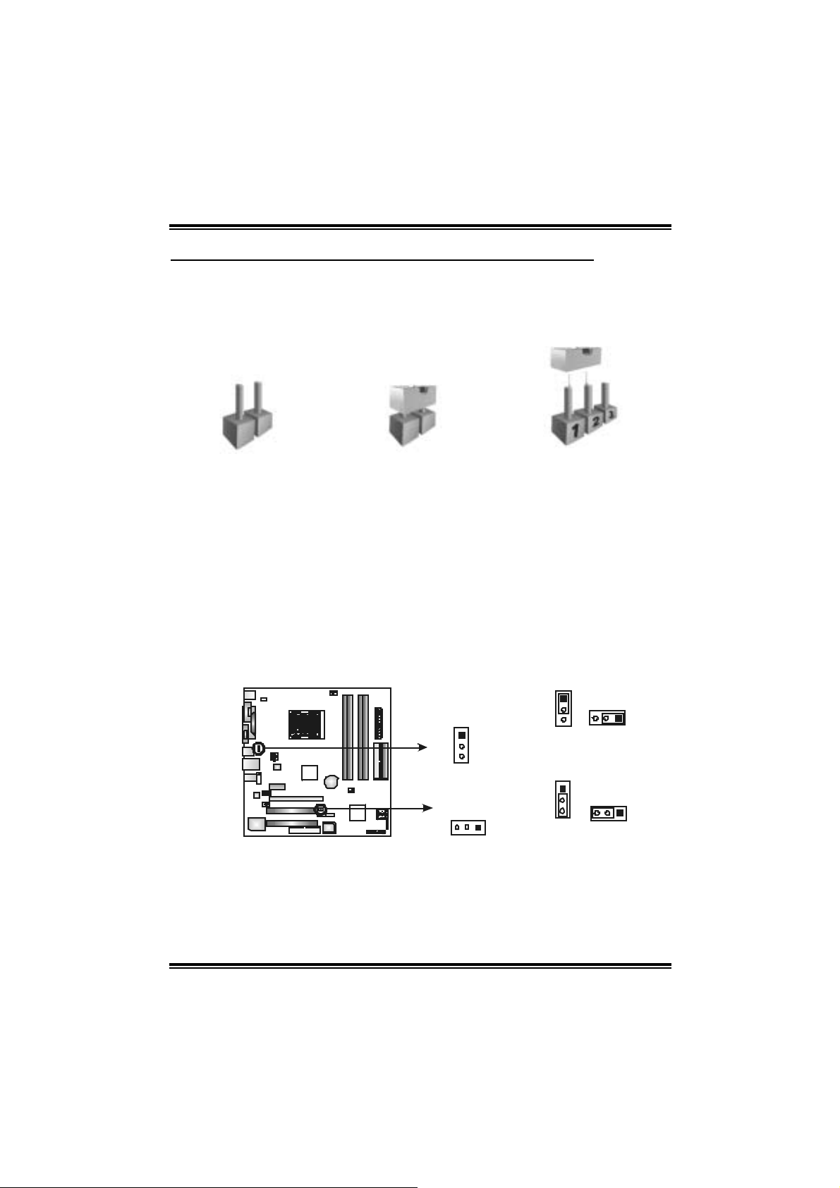
2.2 FAN HEADERS
These fan headers support cooling-fans bui lt in the computer. T he fan
cable and connector may be di fferent according to the fan m anufacturer.
Connect the fan cable to the connector while m atching the bl ack wire to
pin#1.
JCFAN1: CPU Fan Header
JSFAN1 : System Fan Head er
3
1
JCF AN1
31
JSFAN1
Note:
The JCFAN1 and JSFAN1 support 3-pin head c onnector. When c onnecti ng with wires
onto connec tors, pleas e note that the red wire is the positive and should be connected t o
pin#2, and the bl ac k wire is Ground and s hould be c onnected to GND.
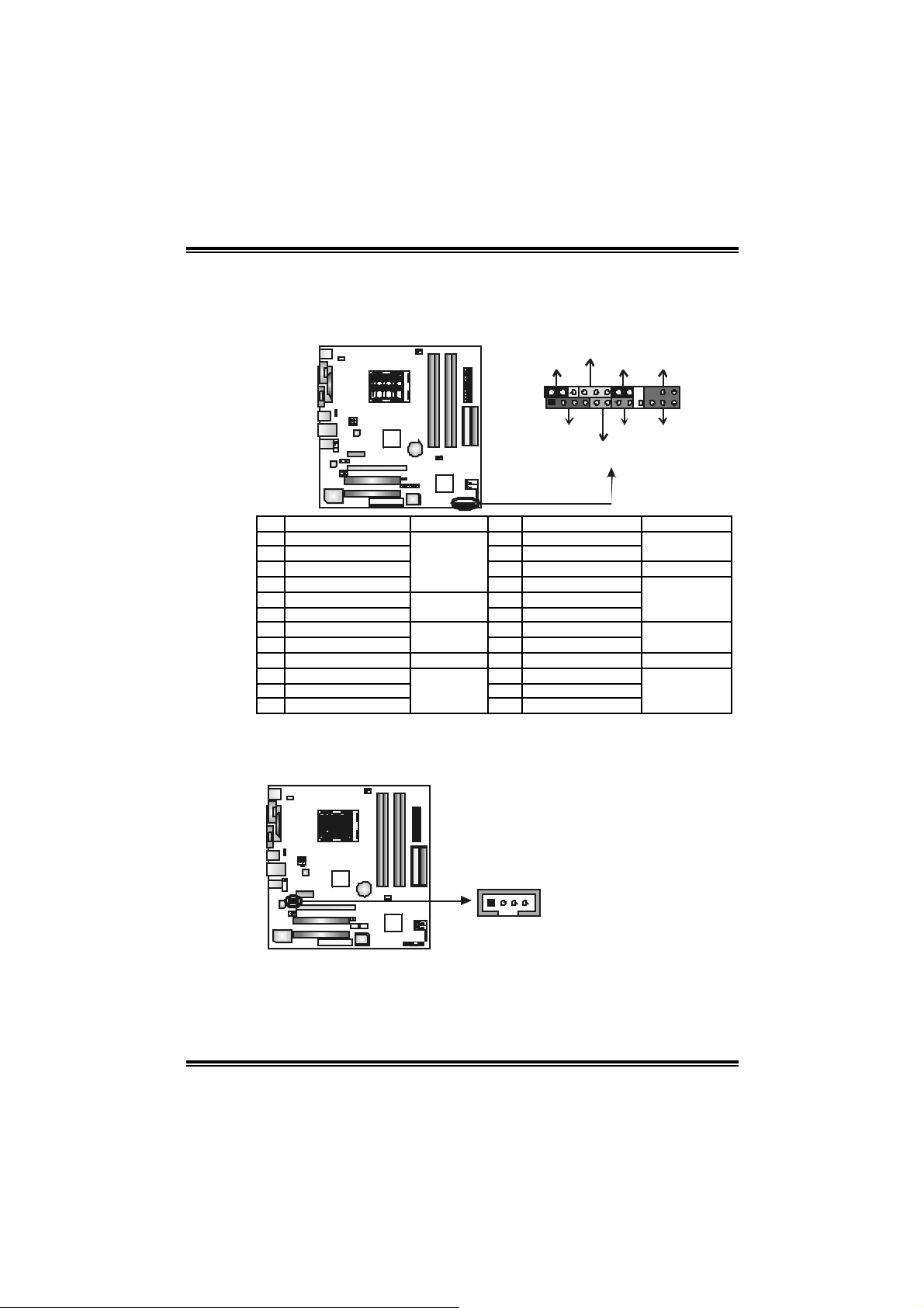
Assignment
Pin
1 Ground
2 +12V
3 FAN RPM ra te
sense
6
Page 9
GeForce 6100-M9
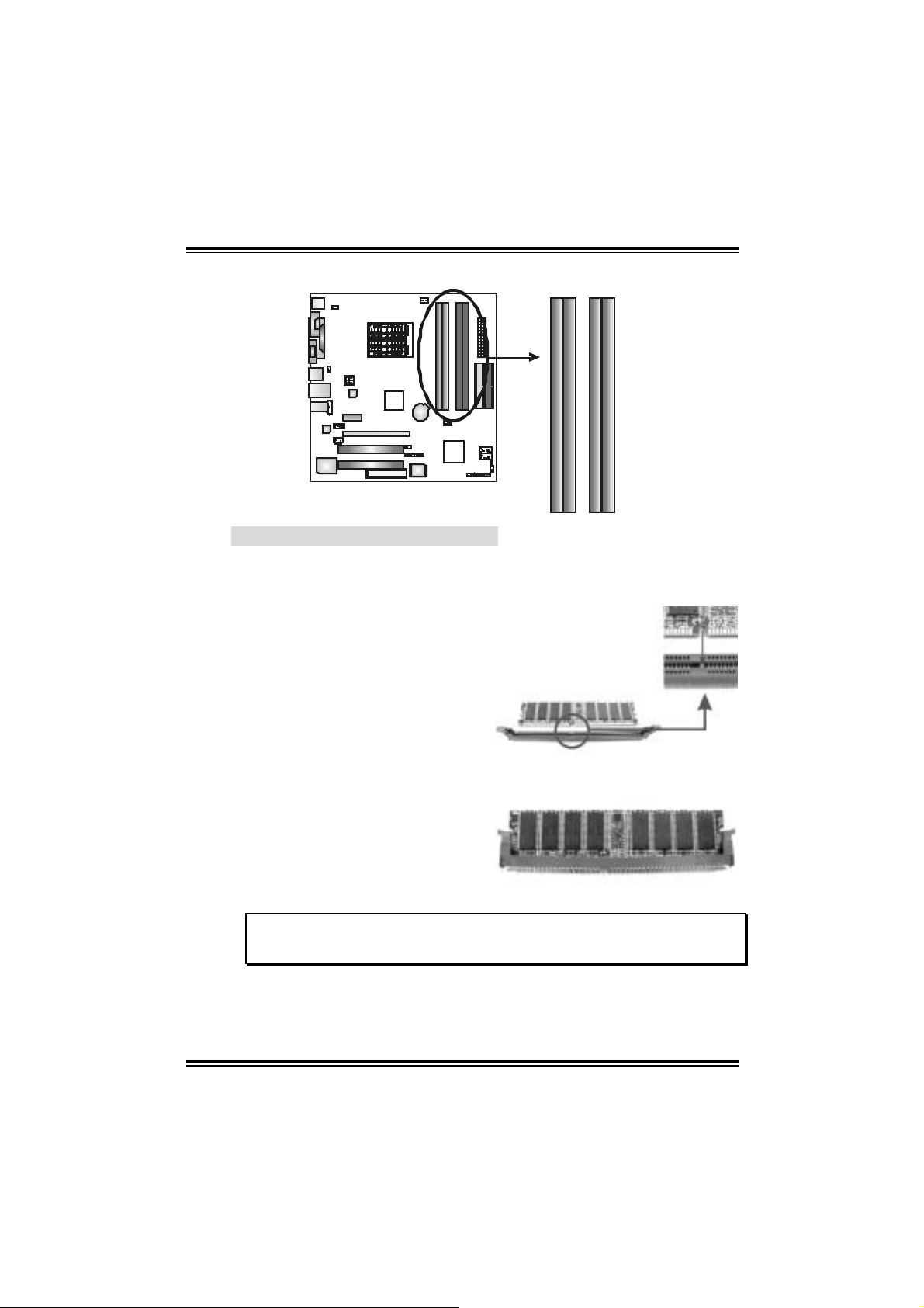
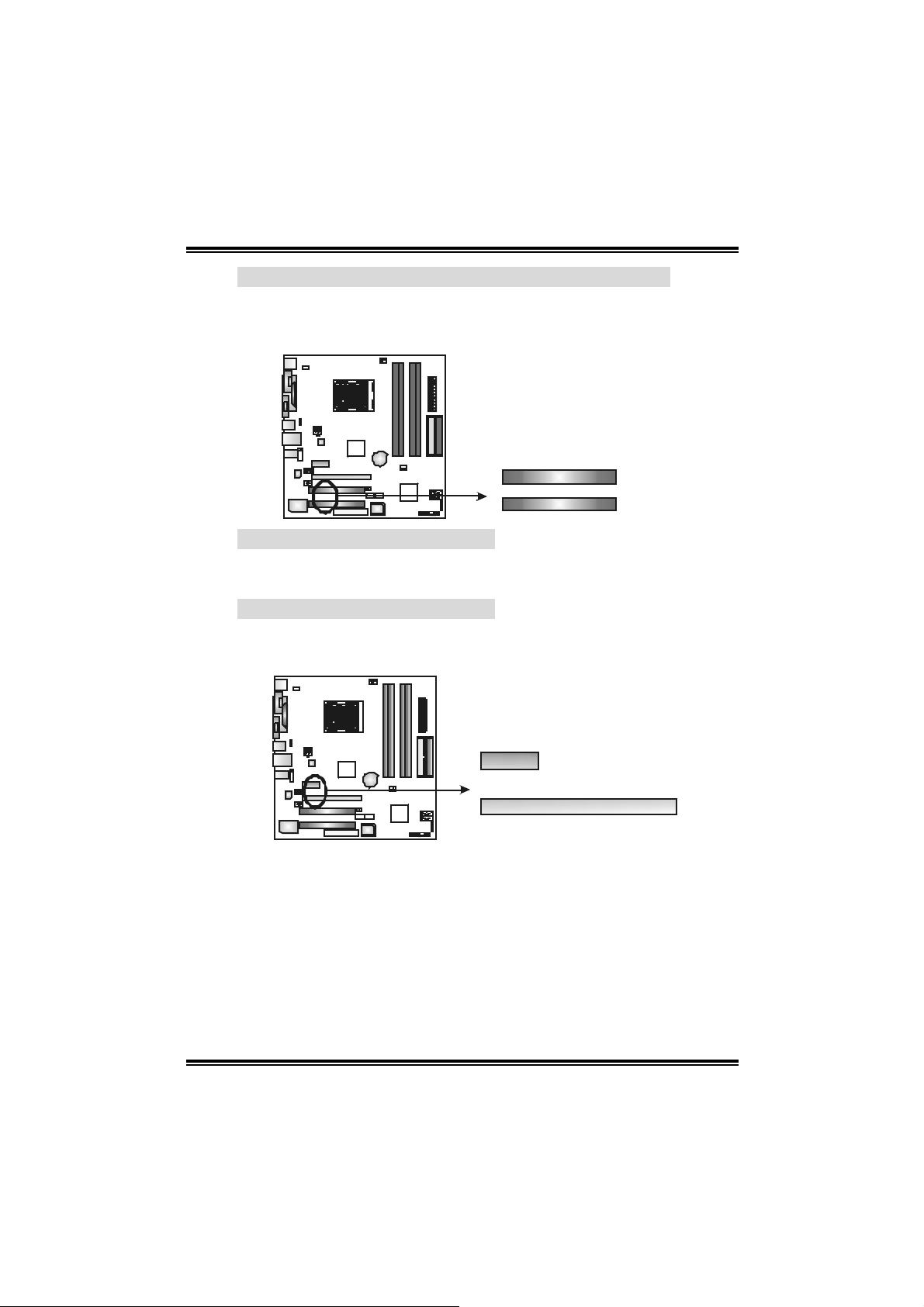
2.3 INSTALL ING SYSTEM MEMORY
DIMMB1
DIMMB2
DIMMA1
DIMMA2
2.2.1 DDR M o dule ins tallat ion
1. Unlock a DIMM sl ot by pressing the retaining clips outward. Align a
DIMM on the slot such that the notch on the DIMM m atches the
break on the Slot.
2. Insert the DIMM vertically and firml y into the sl ot until the retaining
chip snap back in place and the DIMM is properly seated.
Note:
To remove t he DDR modules, pus h the ejector tabs at both sides of the sl ot outward at
the same ti me, and pull the modul es out verticall y.
7
Page 10
GeForce 6100-M9
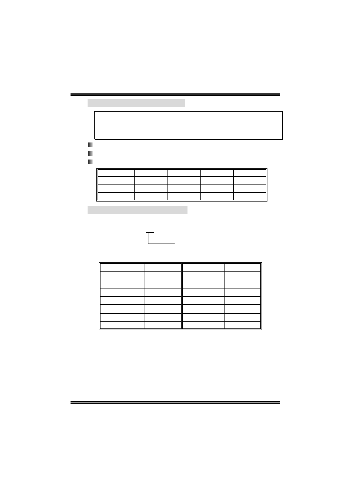
2.2.2 DDR Installation Notice
For AMD K8 939 CPU launched before Rev. E, please follow the table
below to install y our DDR mem ory mod ule, or the system may no t
boot up or m ay not function properl y. (Pl ease refer to Table 1 for CPU
Revision)
“SS ” repre sent s Single Side DDR memo ry module.
“DS” re presen ts Dou ble Side DDR memo ry mod ule.
Star sign “*” represents leave the DIMM socket empty.
DIMMA1 SS/DS
DIMMA2
DIMMB1
DIMMB2
*
* * *
* * *
*
SS/DS SS/DS SS/DS
2.2.3 Know your C PU version
AMD At hl on 64 Processor Orderi ng Part Number Exampl e
ADA 32 00 A E P 5 AP
SS/DS SS/DS
SS/DS
SS/DS
Part Definiti on: AP = Rev C0 (see Table 1)
Ta ble 1: AMD Athlo n 64 Processor Part De fi ni ti on O pti ons
Part Defi ni ti on Revision Part Defi ni ti on Revision
AP Rev C0 BN Rev E4
AR Rev CG BP Rev E3
AS Rev CG BO Rev E3
AW Rev CG BY Rev E6
AX Rev CG BW Rev E6
AZ Rev CG
BI Rev D0
8
Page 11
GeForce 6100-M9
2.4 CONNECTO RS AND SLOTS
FDD1: Floppy Disk Connector
The m otherboard provides a standard floppy di sk connector that
s uppor t s 360 K, 720 K, 1.2M, 1.4 4 M a nd 2.8 8M f lo ppy dis k types.
This connector supports the provided fl oppy drive ribbon cabl es.
33
1
234
IDE1/IDE2: Hard Disk Connecto rs
The m otherboard has a 32-bit Enhanced PCI IDE Control ler that
provides PIO Mode 0~4, Bus Master, and Ultra DMA 33/66/100/133
functionalit y. It ha s two HDD connec tors IDE 1 (primary) and IDE2
(secondary).
The IDE connectors can connect a master and a sl ave drive, so
you can connect up to four hard disk drives. The fi rst hard drive
should always be connected to IDE1.
3940
21
IDE1IDE2
9
Page 12
GeForce 6100-M9
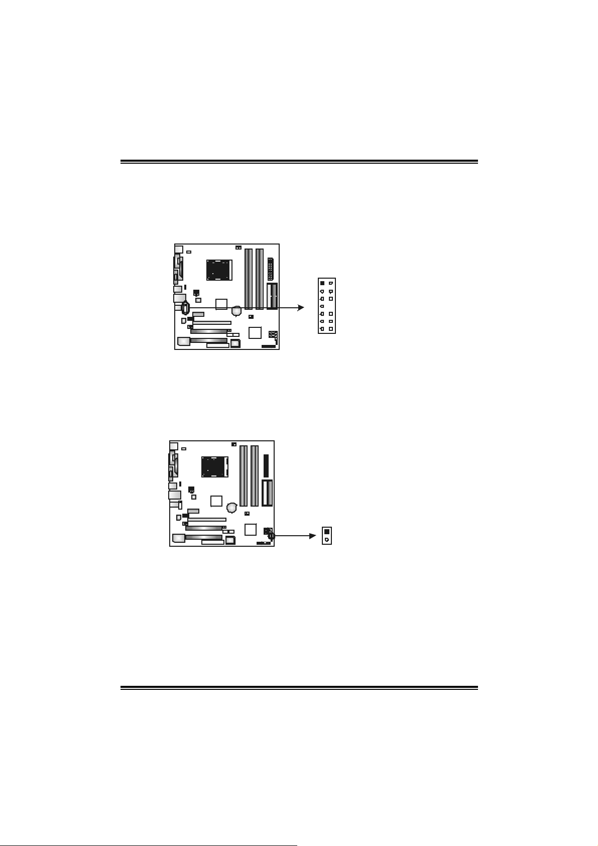
PCI1~PCI2: Perip hera l Component Interconnect Slots
This motherboard is equipped wi th 2 standard PCI slots. PCI stands
for Peri pheral Component Interconnect, and it is a bus standard for
expansi on cards. This PCI slot i s designated as 32 bi ts.
PCI1
PCI2
PCI-EX16: PCI-Ex press x16 Slot
- PCI-Express 1.0a compliant.
- Ma ximum bandwidth i s up to 4GB/s pe r direction.
PCI-EX1_1: PCI-Ex press x 1 Slot
- PCI-Express 1.0a compliant.
- Maximum bandw idth is up to 250MB/s per directi on.
PCI-EX1_1
PCI-EX16
10
Page 13
GeForce 6100-M9
CHAPTER 3: HE ADERS & JUMPERS SETUP
3.1 HOW TO SETUP JUMPERS
The illustration shows how to set up jumpers. When the jumper cap is
placed on pins, the jumper is “cl ose”, if not, that means the jumper is
“open”.
Pin opened Pin closed Pin1-2 closed
3.2 DETAIL SETTINGS
JU SBV1/JUSB V2: Powe r Source Heade rs for USB Ports
Pin 1- 2 Clo se:
JU SBV1: +5V for USB port s at JUSB1 and JU SBLAN 1.
JU SBV2: +5V for USB port s at f ront panel (JUSB2/JU SB3).
Pin 2- 3 Clo se:
JU SBV1: USB ports at JUSB1 and J U SBLAN1 are powered by +5V
JU SBV2: USB ports at front panel (J U SB2/JUSB3) are powered by +5V
standb y vol tage.
standb y vol tage.
JUSBV1
1
3
JUSBV2
31
1
3
Pin 1-2 close (Default)
1
3
Pin 2-3 close
13
3
1
Note:
In order to s upport this function “Power-On sy stem via USB device,” “JUSBV1/ JUSBV2”
jumper cap should be placed on Pin 2-3 individuall y.
11
Page 14
GeForce 6100-M9
JKBV1: Power S ource Header for PS/2 Keyboard an d Mouse
31
Pin 1-2 Close
13
Note:
In order to support this f unction “Power-on system via keyboar d and mouse”, “JKBV1”
jumper cap should be placed on Pin 2-3.
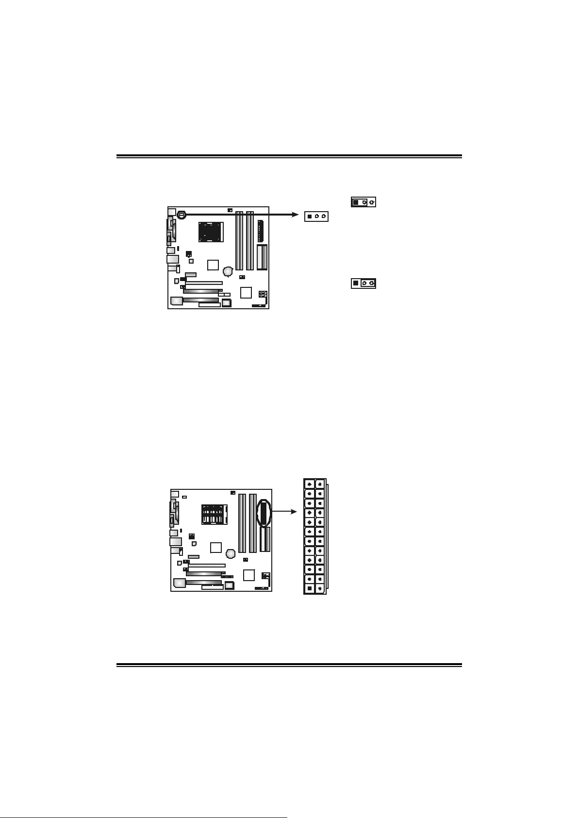
JATXPWR1: ATX Powe r So u rce Conne ctor
This connector allows user t o c onnect 24-pin power connector on the ATX
power supply .
12 24
113
+5V for PS/2 keyboard and
mouse.
1
3
Pin 2-3 close
PS/2 keyboard and mouse are
powered by +5V standby
voltage.
Pin Assignment
1 +3.3V
2 +3.3V
3 Ground
4 +5V
5 Ground
6 +5V
7 Ground
8 PW_OK
9 Standby Voltage
+5V
10 +12V
11 +12V
12 +3.3V
13 +3.3V
14 -12V
15 Ground
16 PS_ON
17 Ground
18 Ground
19 Ground
20 -5V
21 +5V
22 +5V
23 +5V
24 Ground
12
Page 15
GeForce 6100-M9
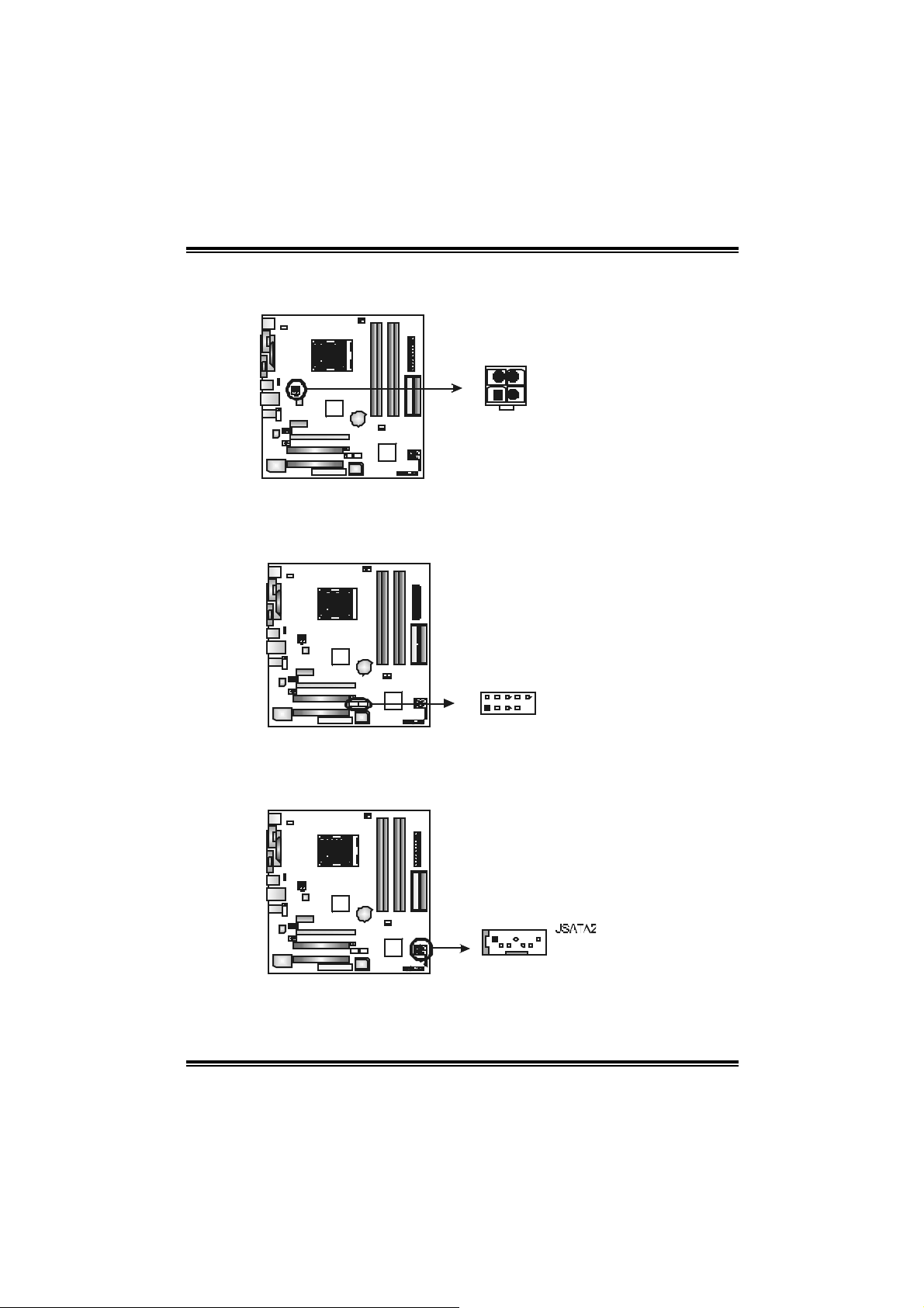
JATXPWR2: ATX Powe r So u rce Conne ctor
By c onnecting this c onnector, it will provide +12V to C PU power c irc uit .
Pin
4
1
1 +12V
3
2 +12V
2
3 Ground
4 Ground
JUSB2/JUSB3: Headers for USB 2.0 Ports at Front Panel
This header allows us er t o connect addit ional USB cable on the PC front panel,
and also can be c onnec t ed wit h internal USB devices, like U SB card reader.
JUSB3JUSB2
2
10
1
9
Assignment
Pin Assignment
1 +5V (fused)
2 +5V (fused)
3 USB4 USB5 USB+
6 USB+
7 Ground
8 Ground
9 Key
10 NC
JSATA1 ~ JS ATA2: Serial ATA Co nnect o rs
The motherboard has a PCI t o SATA C ont roller with 2 channels SATA int erf ace,
it satisfies the SATA 2.0 spec and with transfer rate of 3GB/s.
Pin
Assignment
1 Ground
2 TX+
3 TX4 Ground
174
JSA TA1
13
5 RX6 RX+
7 Ground
Page 16
GeForce 6100-M9
_
JPANEL1: Front Panel Header
This 24-pin connector includes Power-on, R eset, H DD LED, Power LED, Sleep
butt on, speaker and I rD A Connec t ion. It allows us er to c onnect t he PC c as e’s
front panel switch fun ction s.
PWR
SPK
++
HLED
+
LED
On/Off
-
RST
IR
24
23
IR
SLP
2
1
Pin Assignment Function Pin Assignment Function
1 +5V 2 Sleep control
3 N/A 4 Ground
5 N/A 6 N/A N/A
7 Speaker
9 HDD LE D (+) 10 Powe r LED (+)
11 HDD LED (-)
13 Ground 14 Power button
15 Reset control
17 N/A 18 Key
19 N/A 20 Key
21 +5V 22 Ground
23 IRTX
Speaker
Connector
Hard drive
LED
Reset button
IrDA
Connector
8 Power LED (+)
12 Power LED (-)
16 Ground
24 IRRX
Sleep button
Powe r LED
Power-on button
IrDA Connector
JCDIN1: CD-ROM Aud io-in Connector
This connector allows us er to c onnect the audio s ourc e f rom the v ariaty dev ices,
like CD-R OM, D VD -ROM, PC I sound card, PCI TV t urner card etc..
Pin
Assignment
1 Left Channel Input
2 Ground
41
3 Ground
4 Right Channel Input
14
Page 17
GeForce 6100-M9
JAUDIO2: Fron t Panel Audio Header
This header allows us er t o connec t the front audio out put c able with the PC front
panel. It will dis able t he output on back panel audio c onnectors.
Pin Assignment
1 Mic-in/Stereo MIC-in R
2 Ground
3 Stereo MIC-in L
4 Audio power
5 Right line-out/
Speaker-out Right
6 Right line-out/
2
1
14
13
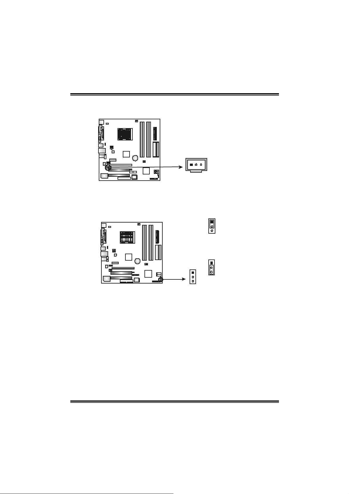
JCI1: Chassis Open Header
This connector allows sy stem to m onitor PC case open stat us. If t he signal has
been triggered, it will rec ord t o the C MOS and show t he message on next
boot-up.
Speaker-out Right
7 Reserved
8 Key
9 Left line-out/
Speaker-out Left
10 Left line-out/
Speaker-out Left
11 Right line-in (optional)
12 Right line-in (optional)
13 Left line-in (optional)
14 Left line-in (optional)
Pin
Assignment
1 Case open signal
2 Ground
15
1
2
Page 18
GeForce 6100-M9
JSPDI F_O UT1: Di gital Audio-out Con nec tor
This connector allows user t o c onnect the PCI bracket SPDIF out put header.
Pin
Assignment
1 +5V
2 SPDIF_OUT
13
JCMOS 1 : C lear CMOS Hea der
By plac ing the jum per on pin2-3, it allows user to rest ore the BI OS s af e set t ing
and the CMOS dat a, please caref ully f ollow t he procedures to avoid damaging
the m otherboard.
3 Ground
1
3
Pin 1-2 Close:
Normal Operation (Default).
1
1
3
3
Pin 2-3 Close:
Clear CMOS data.
※ Clear CMOS Procedures:
1. R em ov e AC power line.
2. Set the jumper to “Pin 2-3 close”.
3. Wait for five seco n ds.
4. Set the jumper to “Pin 1-2 close”.
5. Power on the AC.
6. R es et your des ired pas s word or c lear t he CMOS dat a.
16
Page 19
GeForce 6100-M9
CHAPTER 4: USEFUL HELP
4.1 AWAR D BIOS BEEP CODE
Beep Sound Meanin g
One long beep f ollowed by t wo s hort
beeps
High-low siren sound CPU overheated
One Short beep when system boot-up No error found during POST
Long beeps every ot her s econd No DRAM detected or ins t all
4.2 EXTRA INFORMATION
A. BIOS Update
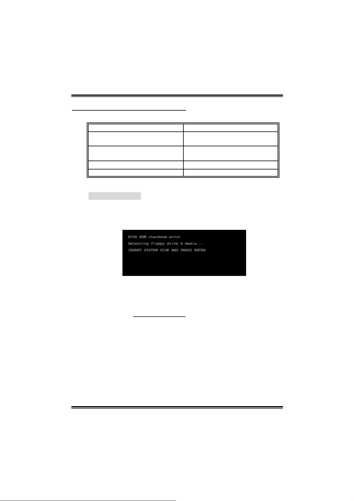
After yo u fail to up d ate BIOS or BIOS is inva ded by virus, the
Boot-Block functi on will hel p to restore BIOS. If the following message
is shown after boot-up the system, it m eans the BIOS contents are
corrupted.
Video card not f ound or v ideo card
mem ory bad
Sys t em will s hut down autom at ic ally
In this Case, pl ease follow the procedure below to restore the BIOS:
1. Make a bo otable fl op py d is k.
2. Download the Flash Utility “AWDFLASH.exe” from the Biostar
websi te: www.biostar.com .tw
3. Confirm motherboard model and download the respecti vel y BIOS
fr om Bi os t ar websit e.
4. Copy “AWDFLASH.exe” and respecti vely BIOS into floppy disk.
5. Insert the bootable disk into floppy drive and press Enter.
6. Sy ste m will boo t-u p to DOS prompt .
7. Type “Awd flash xxxx.bf/ sn/py/ r” in DOS prompt.
(xxxx means BIOS nam e.)
8. Sy ste m will upd ate BIOS au to mati c ally and resta rt .
9. The BIOS ha s bee n recovered an d will work pro pe rly.
17
Page 20

GeForce 6100-M9
B. CPU Overheated
If the system shutdown automatically after power on system for
seconds, that means the CPU protection function has been activated.
When the CPU is over heated, the motherboard wi ll shutdown
automatically to avoid a damage of the CPU, and the system may not
power on again.
In this case, please double check:
1. The CPU cooler surface is placed evenl y with the CPU surface.
2. CPU fan i s rotated normall y.
3. CPU fan speed is ful filling wi th the CPU speed.
After confirmed, pl ease follow steps below to rel ief the CPU protection
function.
1. Rem ove the power cord from power supply for seconds.
2. Wai t for seconds.
3. Plug in the power cord and boot up the system.
Or you can:
1. Clear the CMOS data.
(See “Close CMOS Header: JCMOS1” section)
2. Wai t for seconds.
3. P ower on th e system again.
18
Page 21

4.3 TROUBL ESHOOTING
e
Problem Solution
1. N o power to the system at all
Power light don’t illuminat e, fan
inside power s upply does not turn
on.
2. I ndic at or light on k ey board does
not t urn on.
Sys t em inoperat iv e. Key board light s
are on, power indic at or lights are lit,
and hard drive is spinning.
Sys t em does not boot f rom hard disk
drive, c an be booted f rom opt ic al driv e.
Sys t em only boot s from optical driv e.
Hard disk can be read and applic ations
can be used but boot ing from hard dis k
is imposs ible.
Screen m essage say s “Inv alid
Conf igurat ion” or “C MOS Failure.”
Cannot boot sys t em after inst alling
sec ond hard driv e.
GeForce 6100-M9
1. Make s ure power c able is
sec urely plugged in.
2. Replace cable.
3. Contact techni cal support.
Us ing even pres s ure on both ends of
the DIMM, press down f irm ly unt il t he
module s naps int o plac e.
1. C hec k cable running f rom disk t o
disk controller board. Make s ure
both ends are s ec urely plugged
i n; check t he dr iv e t y pe in the
standard CMOS se tup.
2. Bac k ing up the hard driv e is
ext rem ely im port ant . All hard
disk s are c apable of breaking
down at any t im e.
1. Bac k up data and applic at ions
files.
2. R ef orm at t he hard driv e.
Re-ins t all applicat ions and data
using backup disks.
Rev iew sys t em ’s equipment. Mak e sur
correc t inform at ion is in s et up.
1. Set m aster/slave jum pers
correctly.
2. R un SETUP program and s elec t
correc t drive types. Call t he driv e
manufacturers for co mpatibili t y
with other drives.
19
Page 22

GeForce 6100-M9
CHAPTER 5: WARPSPEEDER™
5.1 INTRO DUCTION
[WarpSpeeder™], a new powerful control utility, features three
user-friendl y functions including Overclock Manager, Overvoltage
Manager, and Hardware Monitor.
Wi th the Overclock Manager, users can easi l y adjust the frequency they
prefer or they can get the best CPU performance wi th just one click. The
Overvol tage Manager, on the other hand, helps to power up CPU core
vol tage and Me mor y v ol tage. The co o l Har dw are Mo ni tor s mar tly in d icates
the temperatures, vol tage and CPU fan speed as wel l as the chi pset
information. Al so, in the About panel , you can get detail descripti ons about
BIOS model and chipsets. In addition, the frequency status of CPU,
mem ory, AGP and PCI along with the CPU speed are synchroni cally
s how n on our ma i n p an el .
Moreover, to protect users' computer systems i f the setting is not
appropriate when testing and results i n system fail or hang,
[WarpSpeeder™] technology assures the sy stem stability by automatically
rebooting the computer and then restart to a speed that i s ei ther the
ori ginal system speed or a suitable one.
5.2 SYSTEM REQUIREMENT
OS Support: Wi ndows 98 SE, Windows M e, Wi ndows 2000, Windows XP
DirectX: DirectX 8.1 or above. (T he Windows XP operating system
includes DirectX 8.1. If you use Wi ndows XP, you do not need to instal l
Dir ec tX 8.1.)
20
Page 23

GeForce 6100-M9
5.3 INSTALL ATION
1. Execute the setup execution file, and then the following di alog will pop
up. Please click “Next” button and follow the default procedure to
install.
2. When you see the followi ng dialog in setup procedure, it m eans setup
is completed. If the “Launch the WarpSpeeder T ray Utility” checkbox
is checked, the Tray Icon utility and [Wa rpSpeeder™] util ity will be
automatically and imm ediately launched after you click “Fi nish”
button.
Usage:
The following figures are just only for reference, the screen printed i n
this user ma nual will chan ge a c c ording to you r motherboard on hand.
21
Page 24

GeForce 6100-M9
5.4 [WARPSPEEDER™] INCLUDES 1 TRAY IC ON AND 5 PAN EL S
1. Tray Icon:
Whenever the Tray Icon utili ty is launched, i t will displa y a little t ray
icon on the right side of Windows Taskbar.
This utility is responsible for conveniently i nvoking [WarpSpeeder™]
Utility. You can use the mouse by clicki ng the left button in order to
invoke [WarpSpeeder™] di rectly from the littl e tray i con or you can
ri ght-click the little tray i con to pop up a popup menu as following
figure. The “Launch Utili ty” item in the popup menu has the same
function as mou se left-clic k on tray ic on an d “Exit” ite m will cl ose
T ray Icon utili ty if selecte d.
22
Page 25

GeForce 6100-M9
2. Main Panel
If y ou click the tra y icon, [Wa rpSpeeder™] util ity will be invoked.
Please refer to th e followi ng figure; the utility’s first window you wi ll
see is Main Panel.
Main Panel conta ins features as follows:
a. D i spl ay th e CPU Speed, CPU exter na l clock, Me m ory clock, AGP cl ock,
and PCI cl ock information.
b. Contains About, Vol tage, Overclock, and Hardware Monitor Buttons for
invoking respective panels.
c. With a us er - fr ie nd ly S t atus An im at io n, it c an represent 3 ov er c l ock
percentage stages:
Man walking→overclock percentage from 100% ~ 110 %
Panther runni ng→overclock percentage from 110% ~ 120%
Ca r racing→overclock percentage from 120% ~ above
23
Page 26

GeForce 6100-M9
3. Vol ta ge Pa nel
Clic k the Vol tage button in Main Pa nel, th e button will be highligh ted
and t he Vol tage Pane l will slide out to up as the foll owing fig ure.
In this panel , you can decide to increase CPU core voltage and
Memory voltag e or not. The d efault setting is “No”. If yo u wa n t to ge t
the best performance of overclocking, we recommend you click the
option “Yes”.
24
Page 27

GeForce 6100-M9
4. Over clock Panel
Clic k the Overclock button in Ma in Panel, the bu tton will be
highlighted and the Overclock Panel will slide out to left as the
fol l owi ng f igur e.
Overclock Panel contains the these fea tures:
a. “–3M Hz button”, “-1M Hz button”, “+1MHz button”, and “+3MHz button”:
provide user the abili ty to do real -time overcl ock adjustment.
Warning:
Manually overclock is pot ent ially dangerous, es pec ially when t he
overc locking perc entage is ov er 110 %. We s t rongly recomm end y ou
verif y ev ery s peed y ou overclock by c lick the Verify button. Or, you c an
just click Aut o ov erclock but t on and let [WarpSpeeder™] aut om atically
gets the best res ult for y ou.
b. “Recovery Dialog button”: Pop up the following dialog. Let user select
a restoring way i f system need to do a fail-safe reboot.
25
Page 28

GeForce 6100-M9
c. “Auto-overclock button”: User can click this button and
[Wa rpS pee de r™ ] will set th e be st and sta ble performa nce an d
frequency automatically. [WarpSpeeder™] utili ty will execute a
series of testing un til system fail. Then syste m will do fail-saf e
reboot by using Watchdog function. After reboot, the
[WarpSpeeder™] utility will restore to the hardware default
setting or load the veri fied best and stable frequency according
to th e Recovery Di alog’s setting.
d. “Verify button”: User can click thi s button and [WarpSpeeder™]
will proceed a testing for current frequency. If the testing i s ok,
then the current freq uency will be sa ved into system regi stry. If
the testing fail, system wil l do a fail-safe rebooting. After reboot,
the [Wa rpSpe ede r™ ] uti lity will restore to the ha rdware de fault
setting or load the veri fied best and stable frequency according
to th e Recovery Di alog’s setting.
Note:
Becaus e the t esting program s, invoked in Aut o-overclock and Verify,
include D irectDraw, D irec t 3D and D irectShow tests, the D irectX 8.1 or
newer runtime library is required. And pleas e make sure your dis play
card’s color depth is High c olor (16 bit ) or True color( 24/32 bit ) t hat is
required for Direct3D rendering.
5. Hardware Monitor Panel
Clic k the Hardwa re Mo nitor bu tton in Main Pa ne l, the bu tton will be
highlighted and the Hardware Monitor panel will slide out to left as
the fo l lowing f igur e.
In this panel , you can get the real-time status information of your
system. The informa tion will be ref reshed every 1 second.
26
Page 29

GeForce 6100-M9
6. About Panel
Click the “about” button in Main Panel , the button will be highlighted
and th e About Pa ne l w il l s l id e out to up as the fo l lowin g f ig ur e.
In this panel, you can get model name and detail inform ation in hints
of all the chipset that are related to overclocking. You can also get
the mainboard’s BIOS model and the Version num ber of
[WarpSpeeder™] utility.
27
Page 30

GeForce 6100-M9
Note :
Because the overclock, overvoltage, and hardware monitor features
are controlled by several separate chipset, [WarpSpeeder™] divide
these features to separate panels. If one chipset i s not on board, the
correlative but ton in Main panel will be disabled, but will not inter fere
other panels’ functions. Thi s property can make [WarpSpeeder™]
utility more robust.
28
Page 31

GeForce 6100-M9 BIOS Setup
BIOS Setup........................................................................................1
1 Main Menu.......................................................................................................3
2 Standard CMOS Features...................................................................................6
3 Advanced BIOS Features ................................................................................... 9
4 Advanced Chipset Features............................................................................... 14
5 Integrated Peripherals ...................................................................................... 17
6 Power Management Setup................................................................................ 23
7 PnP/PCI Configurations ................................................................................... 26
8 PC Health Status ............................................................................................. 29
9 Frequency/Voltage Control............................................................................... 31
i
Page 32

GeForce 6100-M9
BIOS Setup
Introduction
T his manual discu ssed Award™ Setup pr ogram b uilt into the ROM BIOS. T he Set up
program allows users to modify the basic system configuration. This special information is
th en stored in battery -back ed RAM s o tha t it retain s the Set up infor mation w hen th e po wer
is turned off.
T he Award BIO S™ in stalled in your co mpute r sys tem’s RO M (R e ad Only Mem ory) is a
custom version of an industry standard BIOS. This means that it supports AMD processor
input/output system. The BIOS provides critical low-level support for standard devices
such as disk drives and serial and parallel ports.
Adding important has customized the Award BIOS™, but nonstandard, features such as
virus and password protection as we ll as special support for detailed fine-tuning of the
chipset controlling the entire system.
The rest of this manual is intended to guide you through the process of configuring your
system using Setup.
Plug and Play Support
These AWARD BIOS supports the Plug and Play Version 1.0A specification. ESCD
(Extended System Configuration Data) write is supported.
EPA Green PC Support
This AWARD BIOS supports Version 1.03 of the EPA Green PC specification.
APM Support
These AWARD BIOS supports Version 1.1&1.2 of the Advanced Power Management
(APM) specification. Power management features are imp lemented via the System
Management Interrupt (SMI). Sleep and Suspend power management modes are supported.
Power to the hard disk drives and video monitors can be managed by this AW ARD BIOS.
ACPI Support
Award ACP I BIOS support Version 1.0 of Advanced Configuration and Power interface
specification (ACPI). It provides ASL code for power management and device
configuration capabilit ies as defined in the ACPI specification, developed by Microsoft,
Intel and Toshiba.
1
Page 33

GeForce 6100-M9
PCI Bus Suppo rt
This AWARD BIOS also supports Version 2.1 of the Intel PCI (Peripheral Component
Interconnect) local bus specification.
DRAM Support
DDR SDRAM (Double Data Rate Synchronous DRAM) are supported.
Suppo r te d CPUs
T his AW AR D B I O S s u pp o rts t he AM D C P U.
Us i ng Set up
In general, you use the arrow keys to highlight items, press <Enter> to select, use the
<PgUp> and <P gDn> keys to change entries, press <F1> for help and press <Esc> to quit.
The followin g tab le provides more detail about how to navigate in the Setup program by
using the keyboard.
Keystroke Function
Up arrow Move to p revio us item
Down arrow Move to next i tem
Left arro w Move to the ite m o n the left (menu bar )
Right arrow Move to the item on the right (menu bar)
Move Enter Move to the item you desired
PgUp key Increase the numeric value or make changes
PgDn key Decrease the numeric value or make changes
+ Key Increase the numeric value or make changes
- Key Decrease the numeric value or make changes
Esc key Main Menu – Quit a nd not save changes into CMOS
F1 k ey Genera l help o n S etup na viga tio n ke ys
F5 key Load previous values fro m CMOS
F7 key Load the optimized defaults
F10 key Save all the CMOS changes and exit
Status Page Setup Menu and Optio n Page Setup Menu – Exit
Current page and return to Main Menu
2
Page 34

GeForce 6100-M9
1 Main Menu
Once you enter Award BIOS™ CMOS Setup Utility, the Main Menu will appear on the
screen. T he Main Menu allows you to select from several setup functions. Use the arrow
keys to select among the items and press <Enter> to accept and enter the sub-menu.
!! WARNING !!
The information about BIOS defaults on manual (Figure
1,2,3,4,5,6,7,8,9) is just for reference, please refer to the BIOS
installed on board, for update information.
Figure 1. Main Menu
Standard CMOS Features
This submenu contains industry standard configurable options.
Advance d BIOS Features
This submenu allows you to configure enhanced features of the BIOS.
Advanced Chipset Features
This submenu allows you to configure special chipset features.
3
Page 35

GeForce 6100-M9
Integrated Peripherals
This submenu allows you to configure certain IDE hard drive options and Programmed
Input/ Output features.
Power Management Setup
This submenu allows you to configure the power management features.
PnP/PCI Configurations
This submenu allows you to configure certain “Plug and P lay” and PCI options.
PC Health Status
This submenu allows you to monitor the hardware of your system.
Frequency/Voltage Control
This submenu allows you to change CPU Vcore Vo ltage and CPU/PCI clock. (Howe ver,
this function is strongly recommended not to use. Not properly change the voltage
and clock may cause the CPU or M/B damage!)
Lo a d Opti mi ze d De fa u l ts
This selection allows you to reload the BIOS when the system is having problems
particularly with the boot sequence. These configurations are factory settin gs optimized
for this system. A confirmation message will be displayed before defaults are set.
Set Supervisor Password
Setting the supervisor password will prohibit everyone except the supervisor from making
changes usin g the CMOS Setup Utility. You will be prompted with to enter a password.
4
Page 36

GeForce 6100-M9
Set User Password
If the Supervisor Password is not set, then the User P assword will function in the same way
as the Supe rviso r Pa ssw ord. If the Su per visor Password is set and the User Pa sswo rd is
set, the “User” will only be able to view configurations but will not be able to change them.
Save & Exit Setup
Save all configuration changes to CMOS(memory) and exit setup. Confirmation message
will be displayed before proceeding.
Exit Without Saving
Abandon all chan ges made during the current session and exit setup. Confirmation
message will be displayed before proceeding.
Upgrade BIOS
This submenu allows you to upgrade bios.
5
Page 37

GeForce 6100-M9
2 Standard CMOS Features
The items in Standard CMOS Setup Menu are divided into 10 categories. Each category
includes no, one or more than one setup items. Use the arrow keys to highlight the item and
then use the<PgUp> or <PgDn> keys to select the value you want in each item.
Figure 2. Standard CMOS Setup
6
Page 38

GeForce 6100-M9
Main Menu Selections
This table shows the selections that you can make on the Main Menu.
Item Options Description
Date mm : dd : yy Set the system date. Note
Time hh : mm : ss Set the system internal
IDE Primary Master Options are in its sub
menu.
IDE Primary Slave Options are in its sub
menu.
IDE Secondary Master Options are in its sub
menu.
IDE Secondary Slave Options are in its sub
menu.
Drive A
Drive B
Video EGA/VG A
360K, 5.25 in
1.2M, 5.25 in
720K, 3.5 in
1.44M, 3.5 in
2.88M, 3.5 in
None
CGA 40
CGA 80
MONO
that the ‘Day’ automatically
changes when you set the
date.
clock.
Press <Enter> to enter the
sub menu of detailed
options
Press <Enter> to enter the
sub menu of detailed
options.
Press <Enter> to enter the
sub menu of detailed
options.
Press <Enter> to enter the
sub menu of detailed
options.
Select the type of fl op p y
disk drive installed in your
system.
Select the default video
device.
7
Page 39

GeForce 6100-M9
Item Options Description
Halt On All Errors
No Errors
All, but Keyboard
All, but Diskette
All, but Disk/ Key
Base Memory N/A Displays the amount of
Extended Me mory N/A Displays the amount of
Total Memory N/A Displays the total memory
Select the situation in which
you want th e BIOS to sto p
the POST process and
notify you.
conventional memory
detected during boot up.
extended memory detected
during boot up.
available in the system.
8
Page 40

GeForce 6100-M9
3 Advanced BIOS Features
Fig ure 3. Adva nced BIOS Se tup
Boot Seq & Floppy Setup
9
Page 41

GeForce 6100-M9
Removable Device Priority
in these items.
The Choices: Floppy Disks, LS120, USB-FDD0, USB-FDD1, USB-ZIP0, USB-ZIP1,
and ZIP100.
Hard Disk Boot Priority
These BIOS attempt to load the operating system from the device in the sequence selected
These BIOS attempt to load the operating system from the device in the sequence selected
in the se item s.
The Choices: Pri. Master, P ri. Slave, Sec. Master, Sec, Slave, USBHDD0,
USB HDD1, USB HDD2, and Bootable Add-in Cards.
10
Page 42

First/ Second/ Third/ Boo t Other Device
These BIOS attempt to load the operating system from the devices in the
sequence selected in these items.
The Choices: Floppy, LS120, HDD-0, SCSI, CDROM, HDD-1, HDD-2, HDD-3,
ZIP100, LAN, Disabled.
Swap Floppy Drive
For systems with two floppy drives, this option allows you to swap logical drive
assignments.
The Choices: Disabled (default), Enabled.
Boot Up Floppy Seek
Enabling this option will test the floppy dr ives to determine if they have 40 or 80
tracks. Disabling this option reduces the time it takes to boot-up.
The Choices: Enabled (default), Disabled.
Cache Se tup
GeForce 6100-M9
These BIOS attempt to load the operating system from the device in the sequence selected in
these items.
CP U Int ernal C ache
Depending on the CPU/chipset in use, you may be able to increase memory
access time with this option.
Enable d (default) Enable cache.
Disabled Disable cache.
External Cache
This option enables or disables “Level 2” secondary cache on the CPU, which
may improve performance.
Enable d (default) Enable cache.
Disabled Disable cache.
11
Page 43

GeForce 6100-M9
Virus Warning
T his opt ion allow s you to c hoose the Virus Warnin g fea ture t hat is used t o protec t the IDE
Hard Disk boot sector. If this function is enabled and an attempt is made to write to the
boot sector, BIOS will display a warning message on the screen and sound an alarm beep.
Disabled (default) Virus protection is disabled.
Enabled Virus protection is activated.
Quick Power On Self Test
Enabling this option will cause an abridged version of the Power On Self-Test (POST) to
execute after you power up the computer.
Boot Up N umLock Sta t us
Selects the NumLock. State after power on.
Gate A20 Option
Select if chipset or keyboard controller shou ld control Gate A20.
Typematic Rate Setting
When a key is held down, the keystroke will repeat at a rate determined by the keyboard
controller. When enabled, the typematic rate and typematic delay can be configured.
Typematic Rate (Chars /Sec)
Sets the rate at which a keystroke is repeated when you hold the key down.
Type matic Delay (Msec)
Sets the delay time after the key is held down before it begins to repeat the keystroke.
Enable d (default) Enable quick POST.
Disabled Normal POST.
On (default) Numpad is number keys.
Off Numpad is arrow keys.
Normal A pin in the keyboard controller
controls Gate A20.
Fast (default) Lets chipset control Gate A20.
Disabled (default)
Enabled
The Choices: 6 (default), 8,10,12,15,20,24,30.
The Choices: 250 (default), 500, 750, 1000.
12
Page 44

GeForce 6100-M9
Securi ty Optio n
This option will enable only individuals with passwords to bring the system online and/or
to use the CMOS Setup Utility.
System A password is required for the system to boot and is
also required to access the Setup Utility.
Setup (default) A password is required to access the Setup Utility
only.
This will only apply if passwords are set from the Setup main menu.
APIC MODE
MPS Version Control For OS
The BIOS supports version 1.1 and 1.4 of the Intel multiprocessor specification.
Select version supported by the operation system running on this computer.
The Choices: 1.4 (default), 1.1.
OS Select For DRAM > 64MB
A choice other than Non-OS2 is only used for OS2 systems with memory exceeding 64MB.
Small Logo (EPA) Show
T his ite m allows y ou to en able/ d isab le disp lay th e small E P A lo go.
The Ch o ices : En a b le d (default), Disab led.
Summary Screen Show
This item allows you to enable/ disab le display the Summary Screen Show.
The Choices: Disabled (default), Enabled.
Selecting Enabled enables APIC device mode reporting from the BIOS to
the operating system.
The Ch o ices : En a b le d (default), Disabled.
The Choices: Non-OS2 (default), OS2.
13
Page 45

GeForce 6100-M9
4 Advanced Chipset Features
This submenu allows you to configure the specific features of the chipset installed on your
system. This chipset manage bus speeds and access to system memory resources, such as
DRAM. It also coordinates communications with the P CI bus. T he default settings that came
with your system have been optimized and therefore should not be changed unless you are
suspicious that the settings have been changed incorrectly.
Fig ure 4. Adva nce d Chi pse t Setup
Frame Buffer Size
The Choices: 32M (default), 16M, 64M, 128M, Disabled.
PMU
The Choices: Disabled (default), Enabled.
CPU Frequency
This item allows you to select the CPU Frequency.
The Choices: 200.0 (default).
K8<->NB HT Speed
The Choices: Auto (default).1X, 2X, 3X, 4X, 5X.
NB-->SB HT Speed
The Choices: 4X (default).1X, 2X, 3X, 5X.
NB<--SB HT Speed
The Choices: 4X (default).1X, 2X, 3X, 5X.
14
Page 46

GeForce 6100-M9
K8<->NB HT Width
The Choices:↓16 ↑ 16 (default), ↓ 8 ↑ 8.
NB<->SB HT Width
The Choices: ↓8 ↑8 (def ault) , ↓ 16 ↑ 16.
Err94 Enh
Th is item al lows yo u t o ena b le/dis ab le the “s equent ia l Prufe tch F ea tur e” of K8 CPU.
The Cho ice s: Auto (default), Disable.
Onboard GPU
The Choices: Auto (default), Always Enable.
DRAM Configuration
Tim i n g M o de
The Choices: Auto (default), Manual.
Memclock index value<MHz>
The Choices: 200MHz (default).
CAS# Latency
This field specify the cas# latency, i.e. cas# to read data valid.
The Choices: CL=2.5 (default), CL=3.0, CL=2.0
Min RAS# active time (tRAS)
This field specifies the minimum RAS# active time. Typically -45-60 Nsec.
The Choices: 8T (default).
RAS# to CAS# Delay (tRCD)
This field specifies the RAS# to CAS# Delay to read/ write command to the same
bank. Typically -20 Nsec.
The Choices: 4T (default).
15
Page 47

GeForce 6100-M9
Row precharge Time (tRP)
This field specifies the Row precharge Time. Precharge to Active or
Auto-Refresh of the same bank. Typically 20-24 Nsec.
The Choices: 2T (default).
User Config Mode
The Choices: Auto (default), Manual.
1T/2T M emo ry Timing
The Choices: 2T (default).
MIRR mapping mode
The Choices: Continuous (default), Discrete.
CPU Spread Spectrum
The Ch o ices : Disabled (default), Center, Down.
PCIE Spread Spectrum
This item allows you to disable \ enable the SATA spread spectrum function.
The Ch o ices : Disabled (default), Enable.
SATA Spread Spectrum
This item allows you to disable \ enable the SATA spread spectrum function.
The Cho ice s: Disa bled (default), Enabled.
HT Spread Spectrum
The Ch o ices : Disabled (default), Center, Down.
SSE/SSE2 Instructions
The Cho ices: Enabled (default), Disabled.
System BIOS Cacheable
Selecting the “Disabled ” option allows cachin g of the system BIOS ROM at
F0000h-FFFFFh which can improve system performance. However, any
programs writing to this area of memory will cause conflicts and result in
system errors.
The Cho ice s: Disa bled (default), Enabled.
16
Page 48

GeForce 6100-M9
5 Integrated Peripherals
Figure 5. Integrated Peripherals
IDE F unc tion Se tup
If you highlight the literal “Press Enter” next to the “IDE Function Setup” label and then press
the en ter ke y, it will tak e you a s ubmenu w ith th e f ollow in g opt ions :
OnChip IDE Channel 0/1
The motherboard chipset contains a PCI IDE interface with support for
two IDE channels. Select “Enabled” to activate the first and/or second
IDE interface. Select “Disabled” to deactivate an interface if you are
going to install a primary and/or secondary add-in IDE interface.
The Choices: Enabled (default), Disabled.
17
Page 49

GeForce 6100-M9
Prima ry / Secondary /Master / Slave PIO
The IDE P IO (Programmed Input / Output) fields let you set a PIO
mode (0-4) for each of the IDE devices that the onboard IDE interface
supports. Modes 0 to 4 will increase performance progressively.
In Auto mode, the system automatically determines the best mode
for each device.
The Choices: Auto (default), Mode0, Mode1, Mode2, Mode3, Mode4.
Primary / Secondary /Master / Slave UDMA
Ultra DMA/100 functionality can be implemented if it is supported by the IDE
hard drives in your system. As well, your operating environment requires a DMA
driver (Windows 95 OSR2 or a third party IDE bus master driver). If your hard
drive and your system software both support Ultra DMA/100, select Auto to
enable BIOS support.
The Cho ices: Auto (default), Disabled.
IDE DMA Transfer Access
The Choices: Enabled (default), Disabled.
Serial-ATA 1
Enables support for Serial-ATA 1.
The Choices: Enabled (default), Disabled
SATA DMA transfer
The Choices: Enabled (default), Disabled.
Serial-ATA 2
Enables support for Serial-ATA 2.
The Choices: Enabled (default), Disabled
SATA2 DM A transfe r
The Choices: Enabled (default), Disabled.
IDE Prefetch Mode
The Choices: Enabled (default), Disabled.
18
Page 50

GeForce 6100-M9
RAID Configuration
RAID Enable
The Ch oice s: Dis able d (default), Enabled.
SATA1 Primary/Secondary RAID
The Choices: Disabled (default), Enabled.
19
Page 51

Super IO Device
GeForce 6100-M9
POWER ON Function
This item allows you to choose the power on function.
The Choices: Button ONLY (default), Password, Hot Key, Mouse Left, Mouse
Right, Any Key, Keyboard 98.
KB Po wer O n P asswo rd
This item allows you to enter a password with at least 5 characters.
HOT Key Power On
This item allows you to set the hot key to power on system.
The Cho ices: Ctrl-F1 (default), Ctrl-F2, Ctrl-F3, Ctrl-F4, Ctrl-F5, Ctrl-F6,
Ctrl-F7, Ctrl-F8, Ctrl-F9, Ctrl-F10, Ctrl-F11, Ctrl-F12.
Onboard FDC Co ntro ller
Select Enabled if your system has a floppy disk controller (FDC) installed
on the system board and you wish to use it. If install and FDC or the system
has no floppy drive, select Disabled in this field.
The Choices: En a bl ed (default), Disabled.
Onboard Serial Port 1
Select an address and corresponding interrupt for the first and second serial ports.
The Choices: Disabled, 3F8 /IRQ 4 (default), 2F8/IRQ3, 3E8/IRQ4, 2E8/IRQ3,
Auto.
Onboard Serial Port 2
Select an address and corresponding interrupt for the first and second serial ports.
The Choices: Disabled (default), 2F8/IRQ3, 3F8/IRQ4, 3E8/IRQ4, 2E8/IRQ3,
Auto.
20
Page 52

GeForce 6100-M9
UART Mode Select
This item allows you to determine which Infra Red (IR) function of onboard
I/O chip.
The Cho ices : No rmal (default), AS KIR, IrDA.
Full-duplex mode permits s imu ltaneous two-direction transmission.
Th e Ch o ices : Ha lf (def ault), Fu ll.
Onboard Parallel Port
The Choices: 378/IRQ7 (default), 278/IRQ5, 3BC/IRQ7, Disabled.
Parallel Port Mode
The default value is SPP.
The Choices:
SPP (d efault) Us ing P aralle l port as Stand ard P rinter Po rt.
EPP Us ing P a ralle l P ort a s Enh anced Par allel P ort .
ECP Using Parallel port as Extended Capabilities Port.
ECP+EPP Using Parallel port as ECP & EPP mode.
Select a DMA Channel for the port.
The Choices: 3 (default), 1.
OnChip USB
This option should be enabled if your system has a USB installed on the system board.
You will need to disab le this feature if you add a higher performance controller.
The Choices: V1. 1+V2. 0 (default), Disabled, V1.1
USB M emo ry Type
The Choices: SHADOW (default), Base Memory (640k)
USB keyboard Suppo rt
Enables support for USB attached keyboard.
The Choices: Disabled (default), Enabled
USB Mo us e S uppo rt
Enables support for USB attached mouse.
The Choices: Disabled (default), Enabled
UR2 D uple x Mo de
Select the value required by the IR device connected to the IR port.
Half-duplex mode permits transmission in one direction only at a time.
This item allows you to determine access onboard parallel port controller
with which I/O Address.
ECP M o de Use DM A
21
Page 53

GeForce 6100-M9
AC97 Audio
This option allows you to control the onboard AC97 audio.
The Choices: Auto (default), Disabled.
MAC LAN
This option allows you to change the state of the onboard MAC LAN.
The Choice s: Auto (default), Disabled.
Onboa rd LAN Boo t ROM
This item allows you to enable or disable Onboard LAN Boot ROM.
The Choices: Disabled (default), Enabled.
MAC Me dia Interface
The Choices: Pin Strap (default).MII.
Onboa rd 1394
This item allows you to enable or disable the Onboard 1394 Controller.
The Cho ices: Enable d (default), Disabled.
IDE HDD Block Mode
Block m od e is als o called block t ransfer, multip le c omman ds , or multip le se ctor
read / write. If your IDE hard drive supports block mode (most new drives do),
select Enabled for automatic detection of the optimal number of block mode
(most new drive s do), sele c t Ena bled for autom a tic de tection of the optim a l
number of block read / write per sector where the drive can support.
The Cho ices: Enable d (default), Disabled.
POW E R Afte r PW R- F ai l
This setting specifies whether your system will reboot after a power fail or interrupts
occurs.
Off Leaves the computer in the power off state.
On Reboots the computer.
Former-Sts Restores the system to the status before power failure or interrupt occurs.
The Cho ices: Off (default), On, Former-Sts.
22
Page 54

GeForce 6100-M9
6 Power Management Setup
The Power Management Setup Menu allows you to conf igure your system to utilize energy
conservation and power up/power down features.
Figure 6. Power Management Se tup
ACP I f unc tion
This item displays the status of the Advanced Configuration and Power Management
(ACPI).
ACP I S us pend Ty pe
The item allows you to select the suspend type under the ACPI operating system.
Power Manageme nt
This category allows you to select the type (or degree) of power saving and is directly
related to the following modes:
1.HDD Power Down.
2. Suspend Mo de.
There are four options of Power Management, three of which have fixed mode settings
The Choices: Ena bled (default), Disabled.
The Choices: S1 (POS) (default) Power on Suspend
S3 (STR) Suspend to RAM
S1+S3 POS+STR
Min. Power Saving
Minimum power management.
Su spen d Mode = 1 hr.
HDD Power Down = 15 min
23
Page 55

GeForce 6100-M9
Max. Power Saving
Maximum power management only available for sl CP U’s.
Su spen d Mode = 1 min.
HDD Power Down = 1 min.
User De f i ne (default)
Allows you to set each mode individually.
When not disab led, each of the ranges is from 1 min. to 1 hr. except for HDD
Power Down which ranges from 1 min. to 15 min. and disable.
Video Off Method
T his opt ion dete rmines the m an ner in wh ich the mo nitor is goes blank.
V/H S YNC+Blank
T his selection will cause the system to turn off the vertical and horizontal
synchronization ports and write blanks to the video buffer.
Blank Screen
This option only writes blanks to the video buffer.
DPMS (default)
Initia l disp lay po wer ma nagem ent s ignaling.
The Choices: Stop Grant, PwrOn Suspend.
HDD Powe r Do wn
When enabled, the hard disk drive will power down and after a set time of system inactivity.
Al l other devices remain act ive .
The Choices: Disabled (default), 1 Min, 2 Min, 3 Min, 4 Min, 5 Min, 6 Min, 7 Min, 8 Min,
9 Min, 10 Min, 11 Min, 12 Min, 13 Min, 14 Min, 15Min.
HDD Down In Suspend
The Choices: Disabled (default), Enable.
Soft-Off by PWR-BTTN
Pressing the power button for more than 4 seconds forces the system to enter the
Soft-Off state when the system has “hung.”
The Choices: Delay 4 Sec, Instant-Off (default).
WOL (PME#) From Soft-Off
The Choices: Disabled (default), Enabled.
WOR (RI#) From Soft-Off
The Choices: Disabled (default), Enabled.
24
Page 56

GeForce 6100-M9
USB Resume from S3/S4
The Choices: Disabled (default), Enabled.
Power-On by Alarm
When you select Enabled, an alarm returns the system to Full ON state.
The Choices: Disabled (default), Enabled.
K8 Cool’n’ Q uiet Control
This function supports AMD Cool ’n’ Quick function.
The Choices: Disabled (default), Auto.
25
Page 57

GeForce 6100-M9
7 PnP/PCI Configurations
This section describes configuring the PCI bus system. PCI, or Personal Computer
Interconnect, is a system which allows I/O devices to operate at speeds nearing the speed of
the CPU itself uses when communicating with its own special components. This section
covers some very technical items and it is strongly recommended that only experienced
users should make any changes to the default settin gs.
Figure 7. PnP/PCI Configurations
Init Display First
With systems that have multip le video cards, this option determines whether the primary
display uses a PCI Slot or an AGP Slot.
The Cho ices: PCI Ex (default), PCI Slot, Onboard.
Reset Config uration Data
The system BIOS supports the PnP feature which requires the system to record which
resources are assigned and protects resources from conflict. Every peripheral device has a
node, which is called ESCD. This node records which resources are assigned to it. The
system need s to rec ord an d update ESCD to the mem ory lo cations. T hese lo cations (4K)
are reserved in the system BIOS. If the Disabled (default) option is chosen, the system‘s
ESCD will update only when the new configuration varies from the last one. If the Enabled
option is chosen, the system is forced to update ESCDs and then is automatically set to the
“Disabled” mode.The above settings will be shown on the screen only if “Manual” is
chosen for the resources controlled by function.Legacy is the term, which sign ifies that a
resource is assigned to the ISA Bus and provides non-PnP ISA add-on cards. PCI / ISA P nP
signifies that a resource is assigned to the PCI Bus or provides for ISA PnP add-on cards
and peripherals.
The Choices: Disabled (default), Enabled.
26
Page 58

GeForce 6100-M9
Resources Co ntrol led By
By Choosing “Auto(ESCD)” (default), the system BIOS will detect the system resources
and automatically assign the relative IRQ and DMA channel for each peripheral. By
Choosing “Manual”, the user will need to assign IRQ & DMA for add-on cards. Be sure
that there are no IRQ/DMA and I/O port conflicts.
IRQ Resources
This submenu will allow you to assign each system interrupt a type, depending on the type
of device using the interrupt. When you press the “Press Enter” tag, you will be directed to
a submenu that will allow you to configure the system interrupts. This is only
configurable when “Resources Controlled By” is set to “Manual”.
IRQ-3 assigned to PCI Device
IRQ-4 assigned to PCI Device
IRQ-5 assigned to PCI Device
IRQ-7 assigned to PCI Device
IRQ-9 assigned to PCI Device
IRQ-10 assigned to PCI Device
IRQ-11 assigned to PCI Device
IRQ-12 assigned to PCI Device
IRQ-14 assigned to PCI Device
IRQ-15 assigned to PCI Device
PCI / VG A Palette Sno o p
Choose Disabled or Enabled. Some graphic controllers which are not VGA compatible
take the output from a VGA controller and map it to their display as a way to provide boot
information and VGA compatibility.
However, the color information coming from the VGA contr o ller is draw n from the palette
table inside the VGA controller to generate the proper colors, and the graphic controller
need s to know wh at is in th e palette of the VGA controller. T o do this, t he no n-VGA
graphic controller watches for the Write access to the VGA palette and registers the snoop
data. In P CI based systems, where the VGA controller is on the PCI bus and a non-VGA
graphic controller is on an ISA bus, the Write Access to the palette will not show up on the
ISA bus if the PCI VGA controller responds to the Write.
In this case, the P CI VGA co ntr oller s hould not respond to the Write, it should only sno op
the data and permit the access to be forwarded to the ISA bus. The non-VGA ISA graphic
controller can then snoop the data on the ISA bus. Unless you have the above situation,
you should disable th is option.
Disabled (default) Disables the function.
Enabled Enables the function.
27
Page 59

Maximum Payload Size
Set the maximum payload size for Transaction packets (TLP).
The Choice: 4096 (default.)
GeForce 6100-M9
28
Page 60

GeForce 6100-M9
8 PC Health Status
Figure 8. PC Health Status
Chassis Open Warning
This item allows you to enable or disable Chassis Open Warnin g beep.
The Choices: Disabled (Default), Enabled.
Shutdown Temperature
T his item allows y ou to se t up the CPU s hutdo wn Temper ature. T his item o nly effe c tive
under Windows 98 ACP I mode.
The Choices: Disabled (default), 60℃/140F, 65℃/149F, 70℃/158F, 75℃/167F.
Show H/W Monitor in POST
If your computer contains a monitoring system, it will show PC health status during POST
stage. T he item offers several delay time for you to choose.
The Choices: Enabled (default), Disabled.
CPU Vcore/ +1.2V+3.3V/ +5.0V/5V<SB>/ Voltage Battery
Detect the system’s voltage status automatically.
CPU Temperature
This field displays the current temperature of the CPU.
29
Page 61

GeForce 6100-M9
Current CPU FAN Speed
This field displays the current speed of CPU fan.
Current SYS FAN Speed
This field displays the current speed SYSTEM fan.
30
Page 62

GeForce 6100-M9
9 Frequency/Voltage Control
Fig ure 9. F requenc y/Vo ltage Contro l
CPU Vco re
Det ect the syst em’s vo ltage s tatus au tomatica lly.
The Cho ice s: Default (default), +0.15V, +0.10V, +0.05V.
DDR Voltage
This item allows you to select DDR Volta ge Control.
The Choices: 2.66V (default), 2.93V, 2.28V, 2.72V.
31
 Loading...