

Page 1

BenQ Rev 1.0
1
BenQ March (D72)/Amethyst
LT Mobile Phone
Service Manual
BenQ Inc.
Wireless Business Unit
Customer Service Dep.
Tel : +886-(0)2-2799-8800 ext 6687
E-Mail : Roychen@acercm.com.tw
Page 2

BenQ Rev 1.0
2
Contents
l Preface…………………………………………………..……………1
l Theory of Operation
1.GSM system Description…………………………………………7
2.Baseband function description…………………………………12
3.Radio Frequency function description ………………………..44
l Download
1.System requirements and setup ………………………………59
2.Function descriptions……………………………………………61
3.FAQ… ……………….……………….……………………………67
l Disassembly (Level1~Level2)………….………………………….69
l Troubleshooting
Level 1~level 2 repair………………………………………………73
Level 3~level 4 repair………………………………………………74
l Replacement parts
Exploded View (fig1~fig3)………………………………………….95
Spare parts list………………………………………………….…..98
l Service Manual Feedback Form……..…………………………….99
Page 3
BenQ Rev 1.0
3
Preface
This service manual is for the customers who purchase of Acer
March handset . It has several main parts of our handset that include
hardware/software and simple disassembly/assembly procedure
introduction. If you don’t understand some of these sections or any
query about it please kindly use our service manual feedback form and
send it back to our Customer Service Department and we’ll response
your query as soon as possible.
Specifications
Table 1: Radio Frequency
Radio Frequency (900 MHz)
Frequency Range TX 880-915 MHz; RX 925-
960
MHz
Channel Spacing 200 KHz
Number of Channels 174 Carriers x 8 (TDMA)
Modulation GMSK
Duplex Spacing 45 MHz
Frequency Stability +/- 0.1 ppm (Uplink TX)
Power Output 33 dBM Class 4 (2 W peak)
Receiver Level < -102 dBm (Wireless)
Radio Frequency (1800 MHz)
Frequency Range TX 1710-1785 MHz; RX
1805-1880 MHz
Channel Spacing 200 KHz
Number of Channels 374 Carriers x 8 (TDMA)
Modulation GMSK
Duplex Spacing 95 MHz
Frequency Stability +/- 0.1 ppm (Uplink TX)
Power Output 30 dBM – 0 dBM
Receiver Level < -102 dBm (Wireless)
Operating Temperature Range -10 to +55 °C
Page 4
BenQ Rev 1.0
4
Table 2: Voltage Operation
Voltage Operation
Li-ion Battery DC 3.3-4.2 V
Ni-MH Battery DC 3.3-4.2 V
Table 3: Power Consumption
Power Consumption
Working Current Average < 270 mAH
Standby Current 6 +/-0.2 mAH
Talking Time* 120 ~300 min (With Ni-
MH 550
mAH)
Standby Time* 50~120 hours (With Ni-
MH 550
mAH)
DTX / DTR Yes
Table 4: Appearance
Handset Appearance
Dimensions 106 x 40 x 16 mm
Volume 68 c.c.
Handset Weight 99 g
Table 5: Basic Services
Telephony (Speech)
Tele Service
Emergency Call
Delivery Report
Short Message Service MT/MO
Short Message Service
Cell Broadcast
Bearer Service
Data circuit duplex
asynchronous up to 14400
bit/sec
Page 5

BenQ Rev 1.0
5
Scope of Manual
This manual is intended for use by experienced technicians
familiar with similar types of equipment. It is intended primarily to
support electrical and mechanical repairs. Repairs not covered in the
scope of this manual should be forwarded to Motorola’s regional
Cellular Subscriber Support Centers.
Page 6

BenQ Rev 1.0
7
Theory of Operation
△ GSM System Description
General Cellular Concept
The cellular systems are used to provide radiotelephone service in
the frequency range 890-960 MHz. A cellular system provides higher
call handling capacity and system availability than would be possible
with conventional radiotelephone systems (those which require total
system area coverage on every operating channel) by dividing the
system coverage area into several adjoining sub-areas or cells.
Each cell contains a base station (cell site) which provides
transmitting and receiving facilities, for an allocated set of duplex
frequency pairs (channels). Since each cell is a relatively small area,
both the cell site and the radiotelephone that it supports can operate at
lower power levels than would be used in conventional systems.
Using this technique, radiation on a given channel is virtually
contained in the cell operating on that channel and, to some extent,
those cells directly adjacent to that cell.
Since the coverage area of a cell on a given channel is limited to a
small area (relative to the total system coverage area), a channel may
be reused in another cell outside the coverage area of the first. By this
means, several subscribers may operate within the same geographic
area, without interference with each other, on a single channel.
GSM Description
Unlike previous cellular systems, GSM uses digital radio
techniques. The GSM system has the following advantages over
previous analogue systems:
♦International Roaming - Due to international harmonization and
standardization, it will be possible to make and receive calls in any
Page 7

BenQ Rev 1.0
8
country which supports a GSM system.
♦Digital Air Interface - The GSM phone will provide an entirely digital
link between the telephone and the base station, which is, in turn,
digitally linked into the switching subsystems and on into the PSTN.
♦ISDN Compatibility - ISDN is a digital communications standard that
many countries are committed to implementing. It is designed to carry
digital voice and data over existing copper telephone cables. The GSM
phone will be able to offer similar features to the ISDN telephone.
♦Security and Confidentiality – Telephone calls on analogue systems
can very easily be overheard by the use of a suitable radio receiver.
GSM offers vastly improved confidentiality because of the way in which
data is digitally encrypted and transmitted.
♦Better Call Quality - Co-channel interference, handover breaks, and
fading will be dealt with more effectively in the digital system. The call
quality is also enhanced by error correction, which reconstructs lost
information.
♦Efficiency - The GSM system will be able to use spectral resources
in a much more efficient way than previous analogue
Systems
In the figure below, the area bounded by bold lines represents the
total coverage area of a hypothetical system. This area is divided into
several cells, each containing a cell site (base station) operating on a
given set of channels which interfaces radiotele- phone subscribers to
the telephone switching system.
Page 8
BenQ Rev 1.0
9
The radiotelephones themselves are capable of operation on any
channel in the system, allowing them to operate in any cell. Due to the
low power requirements for communications between radiotelephones
in a particular cell and the cell site, operating channels may be
repeated in cells which are outside the coverage area of each other.
For example, presume that cell A operates on channels arbitrarily
numbered 1 through 8, cell B operates on channels 9 through 16, cell C
operates on channels 17 through 24 and cell D operates on channels 1
through 8 (repeating the usage of those channels used by cell A). In
this system, subscribers in cell A and subscribers in cell D could
simultaneously operate on channels 1 through 8.
The implementation of frequency re-use increases the call
handling capability of the system, without increasing the number of
available channels. When re-using identical frequencies in a small area,
co-channel interference can be a problem. The GSM system can
tolerate higher levels of co-channel interference than analogue systems,
by incorporating digital modulation, forward error correction and
equalization. This means that cells using identical frequencies can be
CELL A
CHANNELS
1-8
CELL B
CHANNELS
9-16
CELL C
CHANNELS
17-24
CELL D
CHANNELS
1-8
CELL F
CHANNELS
17-24
CELL E
CHANNELS
9-16
Figure 2: Hypothetical
Page 9

BenQ Rev 1.0
10
physically closer, than similar cells in analogue systems. Therefore the
advantage of frequency re-use can be further enhanced in a GSM
system, allowing greater traffic handling in high use areas.
By incorporating Time Division Multiple Access (TDMA) several
calls can share the same carrier. The carrier is divided into a
continuous stream of TDMA frames, each frame is split into eight time
slots. When a connection is required the system allocates the
subscriber a dedicated time slot within each TDMA frame. User data
(speech/data) for transmission is digitized and sectioned into blocks.
The user data blocks are sent as information bursts in the allocated
time slot of each TDMA frame.
The data blocks are modulated onto the carrier using Gaussian
Minimum Shift Keying (GMSK), a very efficient method of
phase modulation.
Each time an information burst is transmitted, it may be transmitted
on a different frequency. This process is known as frequency hopping.
Frequency hopping reduces the effects of fading, and enhances the
security and confidentiality of the link. A GSM radiotelephone is only
required to transmit for one burst in each frame, and not continually,
thus enabling the unit to be more power efficient.
Each radiotelephone must be able to move from one cell to
another, with minimal inconvenience to the user. The mobile itself
carries out signal strength measurements on adjacent cells, and the
quality of the traffic channel is measured by both the mobile and the
base station. The handover criteria can thus be much more accurately
determined, and the handover made before the channel quality
deteriorates to the point that the subscriber notices.
When a radiotelephone is well within a cell, the signal strength
measured will be high. As the radiotelephone moves towards the edge
of the cell, the signal strength and quality measurement decreases.
Signal information provides an indication of the subscriber’s
Page 10

BenQ Rev 1.0
11
distance from the base station. As the radiotelephone moves from cell
to cell, its control is handed from one base station to another in the new
cell.
This change is handled by the radiotele-phone and base stations,
and is completely transparent to the user.
Service Area
The area within which calls can be placed and received is defined
by the system operators. (Because this is a radio system, there is no
exact boundary that can be drawn on a map.) If the telephone is
outside a coverage area, the (no service) indicator will illuminate and
calls will be unable to be placed or received. If this happens during a
conversation, the call will be lost. There may also besmall areas within
a particular service area where communications may be lost.
The radiotelephone’s identity information is held by its local GSM
system in its Home Location Register (HLR) and Visitor Location
Register (VLR). The VLR contains identity information on all local active
radiotelephones. Should you roam to another area, system or country
the radiotelephones identity information is sent to the VLR in the new
system. The new system will then check the radiotelephones details
with your home system for authenticity. If everything is in order it will be
possible to initiate and receive calls whilst in the new area.
Page 11
BenQ Rev 1.0
12
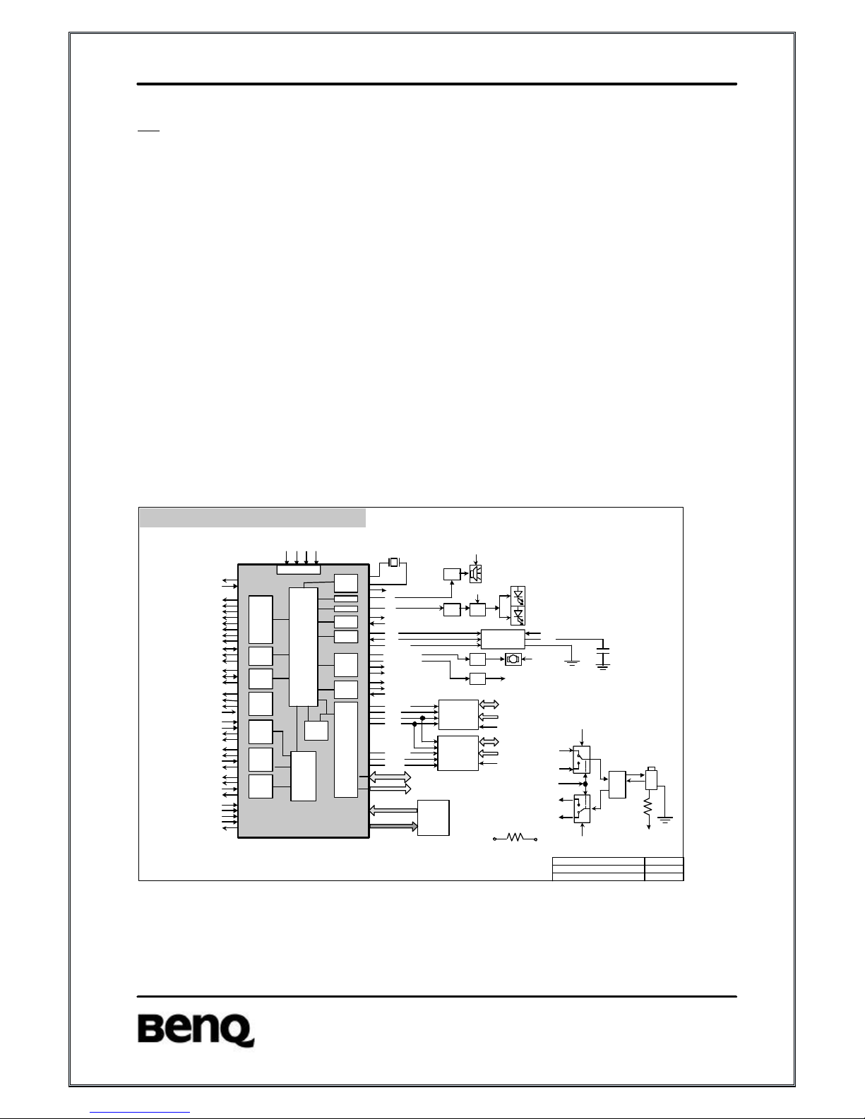
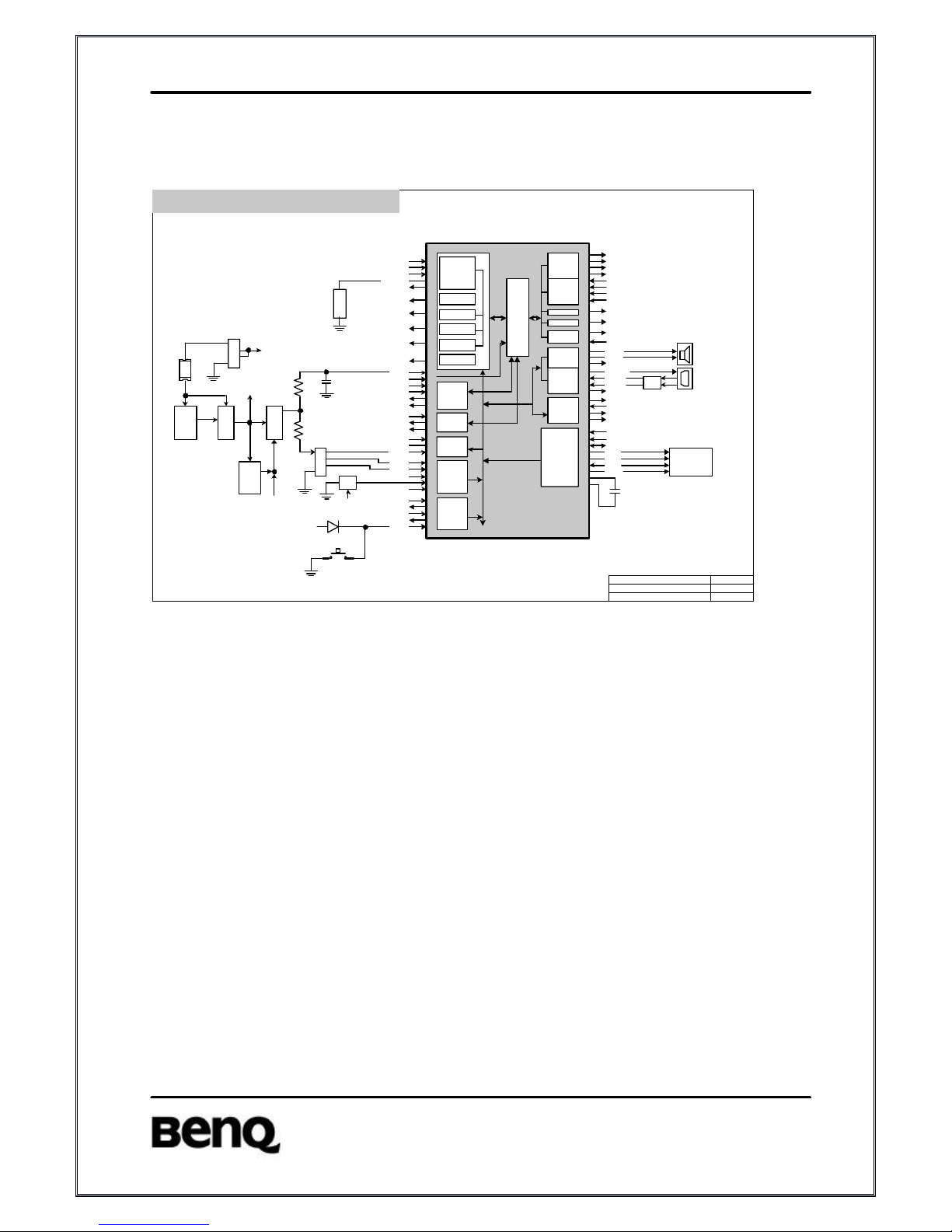
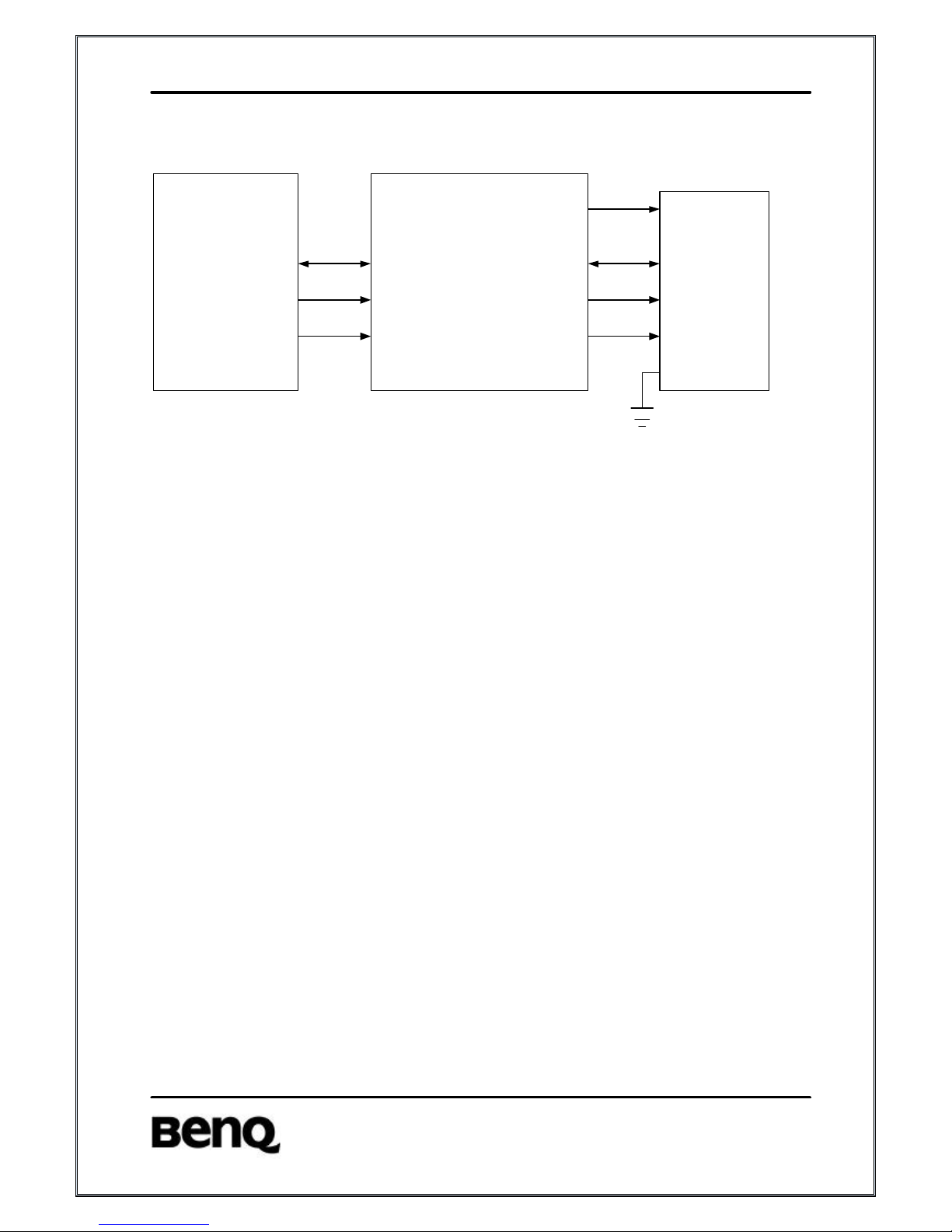
△ Baseband function Descriptions
1. Introduction:
March(T191) utilizes TI’s chipsets (Ulysse and Nausica) as
base-band solution. Base-band is composed with two potions:
Logic and Analog/Codec. Ulysse is a GSM digital base-band logic
solution included microprocessor, DSP, and peripherals. Nausica is
a combination of analog/codec solution and power management
which contain base-band codec, voice-band codec, several voltage
regulators and SIM level shifter etc. In addition, 56D66 integrates
with other features such as LED backlight, LCD display, vibration,
buzzer and charging etc. The following sections will present the
operation theory with circuitry and descriptions respectively.
2. Block Diagram
2.1 Ulysse (Hercules)
JAMES WANG, WEN-SHIH LIU PAGE 1 OF 2
DUAL BAND AMETHYST
BASEBAND BLOCK DIAGRAM REV 1.0
DUAL BAND AMETHYST
SRAM
1Mbit
G5
A2
B5
A1
B2
Flash
Memory
32Mbit
D7
B4
B3
D8
ARM7
RTC
PWT
PWL
UART
I2C
SPI
MEM.
INTF.
GPIO
ACT
TSP
SIM
JTAG
RIF
Voice-
band
INTF
DAI
DSP
2M
SRAM
E10
A11
B6
C2
B1
D2
D3
F4
C4
K11
J1
J3
M6
A7
C7
C8
A8
P6
M9
N8
L8
P7
K8
K7
C6
E6
E9
B11
D11
B12
B13
H10
D14
E14
D13
J14
J13
K14
G1
H1
H3
H2
F12
F13
F14
G13
G11
H12
H13
H11
D8
D9
B9
A9
NROMCS1
FDP
RNW
NFOE
NRAMCS
NBLE
NBHE
MCUEN
MCUDO
MCUDI
IO3DATA_HP_SEL
IO13ACCIN
IO0VIBRATOR
IO1BATID_DET
SCL
SDA
NRSTOUT
TXD0
RXD0
BU
BL
RTCINT
H3
D7
G3
G14
H14
VR1 VR2 VR2B VR3
RX_ON
TX_ON
DCS_T/R
GSM_T/R
BS2
PC
BS1
LE
DATA
CLK
TSPEN0
S_CLK
S_IO
S_RST
TCK
TMS
TDO
TDI
BFSR
BDR
BFSX
BDX
VCLKRX
VDX
VDR
VFSRX
DAI_RST
DAI_CLK
DAI_DI
DAI_DO
TO / FROM
OMEGA
{
TO / FROM
OMEGA
{
JTAG
TO / FROM
OMEGA
{
DAI INTF
{
DATA BUS
DATA BUS
ADDRESS BUS
VR2
DATA BUS
ADDRESS BUS
VR2
}
TO / FROM ULYSSE
LCM
CONT.
4
5
6
7 , 8
1
2 , 3
VR2
VLCD
C34
}
TO EARPHONE JACK
BQ3
BUZZER
U7 BQ2
LCM BACKLIGHT
KEYPAD BACKLIGHT
BQ4 M
U15 BATID
EXTIRQ
EXTFIQ
NRESET
13MHZ
13MOUT
FROM
OMEGA
FROM U61
KEYPAD
POWER
FROM OMEGA
ULYSSE
U1
VIBRATOR
X1 32.768KHZ
E11
D6
TCXOEN
ON_OFF
{
{
{
TO RF BLOCK
TO RF BLOCK
{
TO / FROM
OMEGA
ROW0~ROW3
COL0~COL4
ADDRESS BUS
VBAT
VBATBB
VBAT
U5
U6
TO OMEGA
TO U84,U90
FROM OMEGA
TO OMEGA
TO OMEGA
U9
3
4
2
1
R72
EARPHONE JACK
TXDO
AUXI
IO3DATA_HP_SEL
IO13ACCIN
RXDO
AUXOP
U8
U10
VR2BSW
VR2BSW
MIC
SPK
VR2BSWVR2B
{
U13
M1
Page 12
BenQ Rev 1.0
13
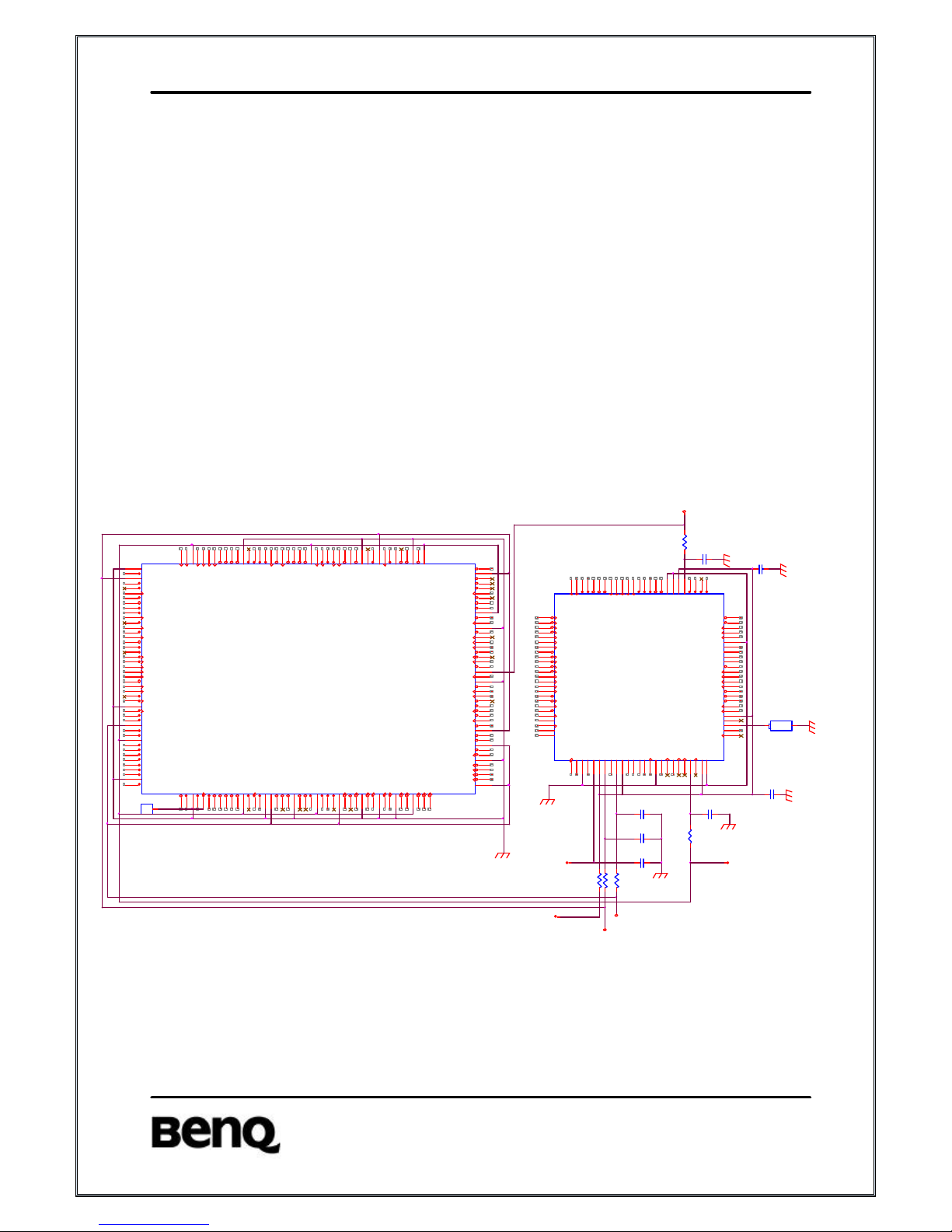
2.2 Nausica (Omega)
IBIC
BUS
CONT.
C4
B3
B2
B4
B5
D4
A2
A1
B1
BSP
K5
J 5
H5
G5
SPI
BCI
ADC
VRPC
F5
K6
J 6
E3
E4
E5
B5
A5
E6
D6
C6
F7
F6
D7
D10
B10
BACKUP
VR1B
2.0V@50mA
VR2B
2.9V@50mA
VR2
2.9V@120mA
VR1
1.8V@120mA
VR3
2.9V@80mA
VREG
B/B
U/L
C9
C10
D8
D9
B/B
D/L
E7
E8
E9
E10
AFC
APC
TSP
VOICE
D/L
VOICE
U/L
USP
SIM REG.
3/5V
SHIFTER
F8
F9
J 4
K4
H8
H9
J 9
K9
J 8
K8
H7
H6
G6
G7
K7
K3
D2
G9
J3
C3
C1
D1
E1
H1
H10
F1
A4
TXIP
TXIN
TXQP
TXQN
RXIP
RXIN
RXQP
RXQN
AFC
RAMP
SMADA
TPENQ
AUXOP
MICBIAS
MICIN
MICIP
AUXI
VCLKRX
VDR
VDSRX
VDX
S_CLK
S_RST
S_IO
CLK
RST
I/O
VSIM
C8
BDX
BFSX
BDR
BFSR
MCUEN0
MCUDO
MCUDI
ICTL
VCHG
VBAT
BATID
TBAT
HWID
EXTFIQ
NRESET
RTCINT
ON_OFF
PWON
VCC1
VCC2
VCC3
VBACKUP
UPR
VR1B
VR2B
VR2
VR1
VR3
OSCAS
EXTIRQ
EARPHONE_IN
SIM
SOCKET
1
3
2
4
}
TO / FROM
ULYSSE
}
}
TO U61
}
FROM U61
TR1
ROW4
S19
EARN
EARP
SPEAKER
MICROPHONE
TO U85
TO U74
}
TO/FROM ULYSSE
{
TO / FROM
ULYSSE
{
TO / FROM
ULYSSE
{
FROM
BATBB
OMEGA
POWER JACK
BATTERY
CONNECTOR
U3
COIN LI-ION
BATTERY
TO / FROM
ULYSSE
1
2
3
4
4
3
2
1
ICTL
VCHG
MANTEST
FUSE
F1
+
_
U4
U14
FROM ULYSSE
C22
TO / FROM
ULYSSE
{
D1
S1
G2
D2
G1
S2
U17
U17
JAMES WANG, WEN-SHIH LIU PAGE 2 OF 2
DUAL BAND AMETHYST
BASEBAND BLOCK DIAGRAM REV 1.0
DUAL BAND AMETHYST
U18
U16
D1
D2
D1
D2
J 1
R21
R24
VR3
VBBATBB
3. Theory:
3.1 Ulysse
ULYSSE (HERCROM200) is a chip implementing the digital
base-band processor of a GSM mobile phone. This chip combines a
DSP M16L80 mega-module (LEAD2 CPU) with its program and data
memories, a Micro-Controller core with emulation facilities
(ARM7TDMIE) and an internal 2M-bit RAM memory, a clock squarer
cell, several compiled single-port or 2-ports RAM and 120K
equivalent CMOS gates.
Major functions of this chip are as follows:
3.1.1 Real Time Clock (RTC)
3.1.2 Pulse Width Tones (PWT)
The function of the PWT is to generate a modulated frequency
signal for the external buzzer.
3.1.3 Pulse Width Light (PWL)
This module allows the control of the backlight of LCD and keypad
by employing a 4096 bit random sequence.
Page 13

BenQ Rev 1.0
14
3.1.4 MODEM-UART
3.1.5 I2C master serial interface (I2C)
In 56D66, we employ I2C bus to control LCD module.
I2C_SCL: programmed to the fast transmission mode (400KHz)
I2C_SDA: the serial bi-directional data of the LCM controller
3.1.6 General Purposes I/O (GPIO)
Ulysse provides 16 GPIOs configurable in read or write mode by
internal registers. In 56D66, we utilize 5 of them as follows:
IO0 : to control vibrator; ‘L’: idle, ‘H’: activate vibrator
IO1 : to identify legal NiMH battery
IO3 : to control phone jack configuration; ‘L’: data cable, ‘H’:
hands-free
IO8 : to support one-wire protocol for Li-Ion battery
IO13 : to detect accessory plug-in at phone jack; ‘H’: idle, ‘L’: plug-in
3.1.7 Serial Port Interface (SPI)
3.1.8 Memory Interface and internal Static RAM
A 2Mbit SRAM is embedded on the die and memory mapped on the
chip-select CS6 of the memory interface.
3.1.9 SIM Interface
3.1.10 JTAG
3.1.11 Time Serial Port (TSP)
3.1.12 TSP Parallel interface (ACT)
In 56D66, we employ 8 of them to control RF activity.
TSPACT1: Band selection 1 (BS1)
TSPACT2: Power control enable (PC)
TSPACT3: Band selection 2 (BS2)
TSPACT4: GSM TR switch on/off (GSM_TR)
TSPACT5: DCS TR switch on/off (DCS_TR)
TSPACT8: RX VCO on/off (RX_ON)
TSPACT9: TX VCO on/off (TX_ON)
TSPACT10: Latch enable (LE)
3.1.13 Radio Interface (RIF)
3.2 Nausica (Omega)
Together with a digital base-band device (Ulysse), OMEGA is part
of a TI DSP solution intended for digital cellular telephone applications
including GSM 900, DCS 1800 and PCS 1900 standards (dual band
Page 14

BenQ Rev 1.0
15
capability).
It includes a complete set of base-band functions to perform the
interface and processing of voice signals, base-band in-phase (I) and
quadrature (Q) signals which support single-slot and multi-slot mode,
associated auxiliary RF control features, supply voltage regulation,
battery charging control and switch ON/OFF system analysis.
OMEGA interfaces with the digital base-band device through a set
of digital interfaces dedicated to the main functions of Ulysse, a
base-band serial port (BSP) and a voice-band serial port (VSP) to
communicate with the DSP core (LEAD), a micro-controller serial port
to communicate with the micro-controller core and a time serial port
(TSP) to communicate with the time processing unit (TPU) for real time
control.
OMEGA includes also on chip voltage reference, under voltage
detection and power-on reset circuits.
Major functions of this chip are as follows:
3.2.1 Baseband Codec (BBC)
3.2.2 Automatic Frequency control (AFC)
3.2.3 Automatic Power Control (APC)
3.2.4 Time serial port (TSP)
3.2.5 Voice band Codec (VBC)
3.2.6 Micro-controller serial port (USP)
3.2.7 SIM card shifters (SIMS)
3.2.8 Voltage Regulation (VREG)
Linear-regulation performed by several low dropout (LDO) regulators
to supply analog and digital baseband circuits.
(1) LDO R1 generates the supply voltage (2.5V, 1.8V, 1.4V and 1.2V)
for the digital core of Ulysse. In 56D66, it is programmed to 1.8V.
This regulator takes power from the battery voltage and it has a
backup through BBS system.
(2) LDO R1B generates the supply voltage 2.0V for the digital core of
OMEGA. It is supplied by the battery.
(3) LDO R2B generates the supply voltage 2.9V for the digital I/O’s of
Ulysse and Omega. It is supplied from battery voltage and has a
backup through BBS system.
Page 15
BenQ Rev 1.0
16
(4) LDO R2 generates the supply voltages 2.9V for Ulysse memory
interfaces I/O’s. It has a backup through BBS system.
(5) LDO R3 generates the supply voltage 2.9V for the analog
functions of OMEGA.
The backup battery switch (BBS) generates at its output an
uninterrupted power rail (UPR) of which purpose is to supply
continuously the minimum necessary circuitry of the power-control
functions either from the main battery of from the backup battery
3.2.9 Baseband Serial Port (BSP)
3.2.10 Battery charger Interface (BCI)
3.2.11 Monitoring ADC (MADC)
3.2.12 Reference Voltage / Power on Control (VRPC)
3.2.13 Internal bus and interrupt controller (IBIC)
3.3 Power Supply circuit
BGND
BGND
VR3
BGND
BGND
BGND
VR2B
BGND
BGND
BGND
VR2
VBATBB
VR1VR1B
TPL16
1
U1
ULYSSE_uBGA179
B2
C2
C3
B1
C1
D3
D2
D1
F5
E4
E2
E3
E1
F4
F3
F2
F1
G5
G4
G2
G3
G1
H1
H3
H2
H4
H5
J1
J2
J3
J4
K1
K3
K2
K4
J5
L1
L2
L3
M1
N1
M3
M2
N2
P2N3P3L4M4N4P4K5L5N5P5M5K6M6P6N6L6K7L7P7N7M7M8N8P8L8K8L9N9P9M9K9M10
P10
N10
L10
K10
P11
N11
M11
L11
P12
N12
P13
N13
M13
M12
N14
M14
L12
L13
L14
K11
K13
K12
K14
J11
J12
J13
J14
H10
H11
H13
H12
H14
G14
J10
G12
G13
G11
G10
F14
F13
F12
F11
E14
E12
E13
E11
F10
D14
D13
D12
C14
B14
C12
C13
B13
A13
B12
A12
D11
C11
B11
A11
E10
D10
B10
A10
C10E9C9A9B9D9E8D8A8B8C8C7B7A7D7E7D6B6A6C6E6C5A5B5D5E5A4B4C4D4A3B3A2
P1
A14
P14
GND
BU/PWT
VDDS2
LT/PWL
SDO/INT10n
RX_MODEM
TX_MODEM
SD_IRDA/CLKOUT_DSP
DSR_MODEM/LPG
RTS_MODEM/TOUT
CTS_MODEM/XF
SCLK/INT1n
RX_IRDA
nSCS0/SCL
RXIR_IRDA/X_A1
TX_IRDA
TXIR_IRDA/X_A4
nSCS1/X_A2
nEMU1
nEMU0
nRESPWRON
TCK
TMS
TDO
TDI
nBSCAN
EN_LMM_PWR/X_IOSTRB
IO0/TPU_WAIT
GND
IO1/TPU_IDLE
ADD0
ADD1
VDDS1
ADD2
ADD3
VDD
ADD4
ADD5
ADD6
ADD7
ADD8
ADD9
ADD10
ADD11
ADD12
ADD13
GNDLMM
ADD14
IO2/IRQ4
ADD15
ADD16
ADD17
ADD18
ADD19
ADD20
VDDLMM
ADD21/CK16X_IRDA
IO3/SIM_RnW
nCS0
GND
VDDS1
nBHE/IO14
nCS1
nCS2
GNDLMM
nCS3
CS4/ADD22
RnW
VDD
nFOE/X_A3
nBLE/IO15
nFWE/X_A0
VDDS1
DATA0
FDP/nIACK
DATA1
GND
DATA2
DATA3
GND
DATA4
DATA5
GNDARM
DATA6
DATA7
VDDARM
DATA8
DATA9
DATA10
DATA11
DATA12
DATA13
DATA14
GND
DATA15
CLK13M_OUT/START_BIT
nRESET_OUT/IO7
TSPACT11/MCLK
VDDS2
SIM_RST
SIM_CD/MAS0
SIM_PWCTRL/IO5
SIM_IO
SIM_CLK
TSPACT10/nWAIT
VFSRX
VDR
VDX
GNDA1
CLKTCXO
VDDS1
VDDA1
BDX
VCLKRX
BCLKX/IO6
BFSX
BDR
BFSR
BCLKR/ARMCLK
TSPCLKX
GND
EXT_IRQ
TCXOEN
VDD
TSPDO
TSPEN0
TSPEN1
TSPDI/IO4
TSPEN2
TSPEN3/nSCS2
TSPACT0
TSPACT1
VDD
TSPACT2
GND
TSPACT3
CLK32K_OUT
GNDA2
OSC32K_OUT
OSC32K_IN
VDDS2
TSPACT4
RFEN/NOPC
GND
TSPACT5
IDDQ
MCSI_TXD/IO9
MCSI_RXD/IO10
MCSI_CLK/IO11
TSPACT6/nCS6
MCSI_FSYNCH/IO12
MCUDI
VDDLMM
MCUDO
MCUEN0
MCUEN1/IO8
MCUEN2/IO13
EXT_FIQ
TSPACT7/CLKX_SPI
ON_OFF
IT_WAKEUP/INT4n
KBC0/NFIQ
TSPACT8/nMREQ
TSPACT9/MAS1
GNDLMM
KBC1/NIRQ
KBC2/XDI_00
KBC3/XDI_01
KBC4/XDI_02
KBR0/XDI_03
KBR1/XDI_04
SDI/SDA
KBR2/XDI_05
VDDLMM
KBR3/XDI_06
KBR4/XDI_07
GND
VDDS2
VDDS1
C21 10UF
C26
0.1UF
C250.1UF
C19 2.2UF
C1710UF
C20 10UF
R22
0
R15
0
U3
OMEGA
B2B1C2C3C1D2D1D3E1E2E3E4E5F1F2F3F4G4G1G2G3H1H2J1K1
J2
K2
J3
H3
K3
J4
K4
H4
K5
J5
H5
G5
F5
K6
J6
H6
G6
G7
K7
J7
H7
K8
J8
K9
K10
A10
B10C9D8D9D10D7E7E8E9
E10F6F7F8F9
F10G8G10G9H10H8H9
J10
J9
A1
A2
B3
A3
C4
B4
A4
D4
D5
C5
B5
A5
E6
D6
C6
B6
A6
C7
A7
B7
A8
C8
B8
A9
B9
C10
SIO3
VS1
GRND2
UPR
VR1BOUT
VCC2
VR2BOUT
VR2SEL
VR2OUT
VR2IN
ICTL
VCHG
VBAT
OSCAS
TESTRESETZ
REFGND
VREF
BGTR1
IBIAS
BGTR3
BGTR2
VR1OUT
BGTR4
FDBK
GRND1
BGTR5
SWITCH
VBACKUP
COMP
VCC1
TDR
TEN
INT2
BDX
BFSX
BDR
BFSR
UEN
UDR
UDX
VCK
VDX
VFS
VDR
AGNDA1
AUXI
MICIP
MICIN
MICBIAS
BUZZOP
RPWON
PWON
BULIP
BULQP
BULQM
ONNOFF
RTC_ALARM
BDLIP
BDLIM
BDLQP
BDLQM
RESPWRONZ
INT1
AFC
APC
DAC
AUXGND
GRND3
VCC3
VR3OUT
EARN
EARP
AUXON
AUXOP
VS2
SVDD
SRST3
VAUX
SCLK3
SCLK5
CK13M
SIO5
SRST5
LCDSYNC
ADIN1
ADIN2
ADIN3
ADIN4/TSCXP
ADIN5/TSCYP
TSCXM
TSCYM
TDO
TDI
TCK
TMS
TEST1
TEST2
TEST3
TEST4
BULIM
R54
0
+-V
U4A
Back-up Battery
2 1
R160R17
0
C15 2.2UF
2.9V@80mA
Omega/Ulysse Analog part
1.8V@120mA
Ulysse Core
2.9V@120mA
Memory
2.9V@50mA
Peripherals
(From Main Battery)
2.0V@50mA
Omega Core
The phone is mainly supplied from the main battery (VBAT)
which is divided into two routes: VBAT is for RF block, vibrator and
buzzer; VBATBB is for baseband block.
The input power (VBATBB) to Nausica is divided into 4 blocks:
Page 16

BenQ Rev 1.0
17
VCC1: to provide power for DC/DC and regulator R1 (VR1)
VCC2: to provide power for regulator R1B (VR1B), R2B (VR2B) and
charger pump
VCC3: to provide power for regulator R3 (VR3)
VR2IN: to provide power for regulator R2 (VR2)
NAUSICA provides five low drop-out voltage regulators.
R1 (VR1): 1.8V@50mA; to supply ULYSSE digital core, RTC,
32KHz and the internal SRAM
R2 (VR2): 2.9V@120mA; to supply 13MHz clock, external memory
devices and LCD display
R2B (VR2B): 2.9V@50mA; to supply peripheral devices, I/O to
NAUSICA
R1B (VR1B): 2.0V@50mA; to supply the digital part of NAUSICA
R3 (VR3): 2.9V@80mA; to supply analog part of NAUSICA.
Among these 5 LDOs, only R1, R2 and R2B are support with
back-up mode.
The power of Ulysse is supplied by these LDOs:
VDD: supplied by VR1 and used for core logic
VDDS1: supplied by VR2 and used for I/Os to memory devices
VDDS2: supplied by VR2B and used for I/Os to Omega and
peripherals
VDDLMM: supplied by VR1 and used for Lead MegaModule (DSP)
VDDARM: supplied by VR1 and used for ARM
Page 17

BenQ Rev 1.0
18
3.4 System power on/off Sequence
3.4.1 Power on
There are three conditions that system can power on.
-On button pushed: A falling edge is detected on PWON pin and the
debouncing time is greater than 30ms.
-Set Alarm: A rising edge is detected on RTC_ALARM (RTCINT)
-Charger plugged: VCHG > VBAT + 0.4V is detected
When these conditions occur in the power on state, the
hardware power on sequence starts:
1. Enable local oscillator OSCAS (~ 100KHz)
2. Enable band-gap (VREF and IREF)
3. Check if Main Battery voltage is greater than 3.2V
4. Enable charge pump (VAUX ~ 5.8V)
5. Enable LDO regulators (R1, R1B, R2, R2B and R3)
6. Set ON_OFF pin to ‘H’.
7. NRESET pin is set from ‘L’ to ‘H’
8. 13MHz clock oscillator is enabled (Ulysse’s task)
3.4.2 Power off in normal mode
When system is powered off in normal mode by long pressing
power-on key, the power off sequence will be executed:
1. Start watchdog timer during 150us and disable DC/DC
2. Set ON_OFF pin to ‘L’
3. Disable all the regulators
4. Disable the band-gap
5. Disable the local oscillator OSCAS
3.4.3 Power off in emergency mode
When the main battery voltage is detected lower than 2.7V, the
following sequence is executed:
1. Set INT1 (FIQ) to ‘L’
2. Start watchdog timer during 150us and disable DC/DC
3. Set ON_OFF pin to ‘L’
4. Disable all the regulators
5. Disable the band-gap
6. Disable the local oscillator OSCAS
Page 18
BenQ Rev 1.0
19
3.5 Memory circuit
DATA BUS
U5
FLASH
U6
SRAM
ULYSSE
CE#
CE1
NROMCS1
NRAMCS
OE#
NFOE
ADDRESS BUS
RP#
WE#
FDP
RNW
OE
HB
LB
NBHE
NBLE
VCCQ
VCC
VCC
VCC
CE2
VR2
VR2
Description
Flash (U5) is a 32Mbit device, supported by VR2 and booted from
top. The total 32Mbits are divided into two sections: 24Mbits is used
for software program code and 8Mbits is used for EEPROM data. The
access time of Flash is 100ns.
SRAM (U6) is a 1Mbit device, supported by VR2. The access time of
SRAM is 70ns.
Page 19
BenQ Rev 1.0
20
3.6 Display circuit
VR2
BGND
NRSTOUT
I2C_SDA
I2C_SCL
R27
1K
C33
1UF(0603)
C32
C(0603)
J2
LCD
1
2
3
4
5
6
7
8
9
10
VLCD
VSS
VSS
SCL
SDA
/RES
VDD2,3
VDD1
X
X
C50
39PF
C51
39PF
C34
1UF(0805 Z5U 16V)
2.9V
400KHz
7.6V
From U1/Ulysse
Description
Display circuit is composed of a 98*64 resolution LCD module and
a display supply voltage bypass capacitor C34. The power of LCDM is
supplied from VR2. It is controlled by U1 via I2C bus: SCL and SDA.
The data rate of I2C is programmed to 400KHz. NRESTOUT is low
active to reset all LCD registers. The LCD Module is adopted with
COG (chip on glass) type, and default display supply voltage VLCD at
normal temperature is 7.6V. R27 is used for ESD protection and C50,
C51 are used for radiation suppression.
Page 20
BenQ Rev 1.0
21
3.7 Vibrator circuit
BGND
VBAT
IO0VIBRATOR
R49
15
R46
1K
A
-
+
M1
LA4-432
12
BQ4
UMT4401
2
1
3
D14
DAN222
2
1
3
3.6V
94mA
1.2V
From U1/Ulysse
Description
To enable vibration, Ulysse sets IO0VIBRATOR to ‘H’ to activate
the motor. R46 and R49 are used to make BQ4 working in saturation
area. D14 is used to feedback EMF. Under the condition of VBAT =
3.6V, the average voltage across the motor is about 1.2V and drain
current is around 94mA.
Page 21
BenQ Rev 1.0
22
3.8 Buzzer circuit
VBAT
BGND
BGNDBGND
BU
BUZZOP
C59
8PF
D14
DAN222
2
1
3
U13
BUZZER
3
4
R48
0
R45
1K
BQ3
UMT4401
2
1
3
T10
TVS
1 2
. .
D16
DAN222(N.M.)
2
1
3
R71
0
3.6V
78mA
1.3V
From U1/Ulysse
(PWT)
(Not In Use)
Description
To alert the buzzer, Ulysse applies PWT (Pulse Width Tone) signal
at BU to drive the buzzer. R45 and R48 are used to make BQ3
working in saturation mode. D14 is used to feedback EMF. Under
the condition of VBAT = 3.6V, the average current is 78mA and terminal
voltage of buzzer is about 1.3V.
Page 22

BenQ Rev 1.0
23
3.9 LED circuit
BGND
VBATBB
BGND
BGND
BL
BQ2
UMT4403
2
1
3
D8
19-21
D7
19-21
D9
19-21
D5
19-21D619-21
R34
2K
D10
19-21
R35
24 (0805)
U7
UMH10N(SOT363)
1 6
2
3 4
5
D11
19-21
D12
19-21
D3
22-21
D13
22-21
D4
22-21
R40
39 (0805)
3.6V
From U1/Ulysse
3.35V
60mA37mA
1.9V
(PWL)
Description
56D66 employs three LEDs for LCD module backlight and eight
LEDs for keypad backlight. To light up the LEDs, Ulysse applies PWL
(Pulse Width Light) at BL to drive LEDs. U7 is used as an inverter to
enable BQ2. Under the default condition (VBAT=3.6V), the average
current of one LCD backlight LED is about 12mA and of one keypad
backlight LED is about 7.5mA. In 56D66, all the LEDs are yellow-green
color and forward voltage is 1.9V
Page 23
BenQ Rev 1.0
24
3.10 Audio circuit
Uplink:
MICIP
MICIN
BGND
MICBIAS
BGND
BGND
C43
4.7UF(0805)
R43
1K
C44 1UF(0603)
X2
Microphone
1
2
3
1
2
3
C54
47PF
R44
4.3K
C42
0.1UF
C45 1UF(0603)
R47
4.3K
U14
EMIF01-10005W5
1
2
34
5
I1
GND
I2O2
O1
R50 0
C53
47PF
R51 0
2.5V
From U3/Omega
To U3/Omega
To U3/Omega
Downlink:
EARN
EARP
BGND BGND
BGND
C39
100PF
BL2 0
BL3 0
R74
10
LS1
SPEAKER_0
C41
150PF
U12
EMIF01-10005W5 (N.M.)
1
2
3 4
5
I1
GND
I2 O2
O1
C40
150PF
R73
10
T4
TVS
1 2
. .
T3
TVS
1 2
. .
From U3/Omega
From U3/Omega
Description
The audio circuit is divided into two parts, uplink and downlink.
For uplink path, the analog voice signals are fed into NAUSICA
from the microphone differential input and then transmitted to Ulysse
DSP via the voice-band series port (VSP). After being modulated, the
signals go through the uplink I/Q path to the RF transceiver and
transmitted from the antenna.
The microphone circuit is biased from Nausica MICBIAS (2.5V).
The bias circuit R43, R44, R47 mainly provides the optimal operation
point for the microphone signals, MICP and MICN.
For downlink path, the signals received from the antenna are
down-converted to I/Q signals and then transmitted to Ulysse DSP.
After being demodulated, the signals are fed to NAUSICA via
voice-band interface and then amplified to drive the receiver.
Page 24

BenQ Rev 1.0
25
3.11 Charging circuit
BGND
BGND
BGND
VBATBB
VBAT
VR3
BGND
BGND
BGND
BGND
BGND
BGND
BGND
BGND
BGND
CHARGERIN
TBAT
VCHG
BATID_NIMH
IO8ONEWIRE
ICTL
G1
S2 G2
D2S1D1
U17
FDC6506P
1 6
3 4
52
C28
C
C31
0.1UF
G1
S2
G2
D2
S1
D1
U18
FDG6303N
1 6
3 4
52
R70 0
R66
3.9M
R67
200K
C48
4.7UF(0805)
R68 0
D15
RB520S-30
1 2
G1
S2
G2
D2
S1
D1
U16FDG6303N
1 6
3 4
52
R65
43K (1%)
R63
470K
R62
470K (1%)
R60
6.2K
F1
FUSE(1A 0603)
C49
1K
T1
TVS
12
..
T5
TVS
12
..
J1
Power Jack
1
2
3
4
V+
SW
SW
GND
J5
0
1
2
3
C56
10UF(0805)
R24
0.2(1%) 0805
D1
CRS03
1 2
C30
100PF
R25
47K
JP1
BATTERY CONN
4
3
2
1
C29
10UF(0805)
C47
0.1UF
C57
1000PF
C55
0.1UF
R64
100K
C58
1000PF
Trigger Charging Circuit
Charger Over-voltage Protection Circuit
Main Charging Route
To U3/Omega To U3/Omega
Description
The charging circuit of 56D66 is composed of charger over-voltage
protection circuit, 3-sec trigger charging circuit and main charging
circuit that are controlled by Omega (U3). 56D66’s charging devices
are standard linear 3.6V/600mA charger and switching VPA (cigarette
charger) with 6V/400mA output.
The group of R62, R65, R63 R64, R70, C47 and U16 compose the
charger over-voltage protection circuit. The cut-off voltage is 8V.
While the charger voltage is over 8V, the circuit will turn off U17 by
latching U17.G1 to stop charging.
The group of D15, R66, C48, R67 and U18 compose the 3-sec
trigger charging circuit. At the very beginning of charging, the circuit will
force to turn on U17 to full charger the battery which can prevent from
long charging wake-up for deep discharge battery. After around 3
seconds, software will take over the charging task by controlling ICTL.
Page 25

BenQ Rev 1.0
26
F1 is a 1A fuse to assure charging current under limit.
The normal charging operation theory is that Omega monitors
charger voltage via VCHG pin to decide whether charger plug in or out,
and control power P-MOSFET (U17) via ICTL pin. If phone enters into
charging mode, Ulysse will follow the charging algorithm to control
charging circuit and monitor charging current by detecting the terminal
voltage of R24 (0.2 ohm). Omega control procedure is classified into
two parts according to whether battery voltage is higher than 3.2V.
Omega will execute trickle charge with 20mA to charge battery via
VCHG pin if battery voltage is lower than 3.2V. On the other hand, the
phone will proceed normal charging task following by the charging
algorithm.
Page 26
BenQ Rev 1.0
27
3.12 Earphone jack circuit
IO3DATA_HP_SEL
VR3
IO13ACCIN
AUXI
EARPHONE_INRXD0
MICBIAS
TXD0
AUXOP
BGND
BGND
BGND
BGND
BGND
VR3
VR2B_SW
BGND
BGND
VR2B_SW
BGND
T9
TVS
1 2
. .
T8
T
1 2
. .
R76
0
U8
NC7SB3157
1
3
2
4
5
6
B1
B0
GndAVcc
S
BL1
BEAD(0603)
R36
10K
T2
TVS
1 2
. .
C37
4.7UF(0805)
R72
1K
J3
Audio Jack
12
3
4 5
GNDSW
SPK
MIC MIC
R37
2K
R38
1K
R41
2K
U9
EMIF01-10005W5
1
2
3 4
5
I1
GND
I2 O2
O1
U10
NC7SB3157
1
3
2
4
5
6
B1
B0
GndAVcc
S
C38
1UF(0603)
BL4
22
J4
0
1
2
3
TP33
1
R32
100K
L: Download
H: Earpiece
active
Plug-In
2.9V
2.9V
V= 1.0 ~ 2.4 => Hands-free
V= 2.6 ~ 2.8 => Data Cable
(To U3/Omega)
2.9V
(Not In Use)
For Data Cable
For Hands-Free
(From U1/Ulysse)
Description
The earphone Jack circuit is used either for the headset or the data
service. The IO13ACCIN will be pulled to low level when headset or
data cable is plugged in. Here, U8 and U10 are used as the switch
between headset using or data service using which is controlled by the
IO3DATA_HP_SEL. When IO13ACCIN is detected as low level,
IO3DATA_HP_SEL is switched from low to high level to identify whether
the headset or the data cable is plug-in by reading the voltage at
EARPHONE_IN. If the voltage at EARPHONE_IN is in the range of
1.0V to 2.4V, the phone recognizes headset is plugged in and
IO3DATA_HP_SEL stays at high to keep U8 and U10 as auxiliary audio
path. If the voltage at EARPHONE_IN is in the range of 2.6V to 2.8V,
the phone identifies data cable plugged in and IO IO3DATA_HP_SEL
switches back to low to keep U8 and U10 as data service path.
Page 27
BenQ Rev 1.0
28
3.13 Rader circuit
OMEGA
SCLK5
SIO5
SRST5
SVDD
RST
CLK
VCC/VPP
GND
I/OSIO3
SCLK3
SRST3
SIM_IO
SIM_CLK
SIM_RST
ULYSSE
SIM
SOCKET
Description
The SIM follows the GSM and ISO specifications and works in 3
volts or in 5 volts with a minimum external logic.
SIM_IO(I/O): Data
SIM_RST(O): Reset signal
SIM_CLK(O): Clock (1.6MHz/3.2MHz)
The SIM card digital interface insures the translation of logic levels
between ULYSSE and SIM card. There is a level shifter embedded in
Omega to support 5V SIM card.
Page 28
BenQ Rev 1.0
29
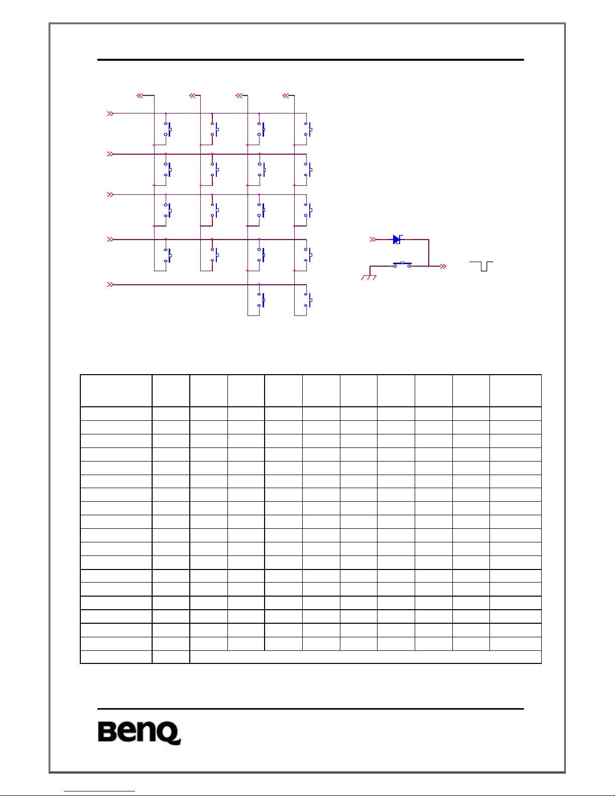
3.14 Keyboard circuit
BGND
ROW2
COL2
COL3
COL1
ROW4
ROW3ROW0
COL4
ROW1
COL0
PWON
S1
KSW
[3]
S7
KSW
[4]
S2
KSW
[2]
S16
KSW
[#]
S10
KSW
[7]
S3
KSW
[1]
S9
KSW
[8]
S6
KSW
[5]
S5
KSW
[6]
S4
KSW
[Down]
D2
RB520S-30
1 2
S13
KSW
[0]
S15
KSW
[menu]
S19
KSW
[NO]
[PWR]
S14
KSW
[*]
S8
KSW
[SEL]
S17
KSW
[Send]
S12
KSW
[9]
S18
KSW
[QUIT]
S11
KSW
[Up]
To U3/Omega
Description
1. The keypad is made of a 5 Column x 4 Row matrixes.
2. The keypad matrix is as follows:
Function Key
COL0 COL1 COL2 COL3 COL4 RO
W0 ROW1 ROW2
ROW3
3 S1 0 0
2 S2 0 0
1 S3 0 0
DOWN S4 0 0
6 S5 0 0
5 S6 0 0
4 S7 0 0
SEL S8 0 0
8 S9 0 0
7 S10 0 0
UP S11 0 0
9 S12 0 0
0 S13 0 0
* S14 0 0
MENU S15 0 0
# S16 0 0
SEND S17 0 0
QUIT S18 0 0
NO/PWR S19
Reference Drawing:
Page 29

BenQ Rev 1.0
31
56D72 Side 1 Layout
U2
RN4
RN2
RN1
RN3
D2
R1
R26
C1
C2
R56
R52
R59
R58
R57
RN5 RN6
C13
R14
U7
BQ2 U14
C35
R34
C54
C53
C44
C45
C55
T1
R51
R50
R44
C43
C48 U18
D15
D1
R24
C29 C56
R66
R67
R25
C36
C42
TR1
R43
R47
R19
C4
C5
R5 R8
R7
R9
C7
R6
R28 R29 R13
R15
R17
R18
R16
C9
R21
C24 R20
C25
C18
C6
R77
C22
R4
R23
C46
C23
C8
C19 C20
C21
C17
C15
R41
R22
C12
C11
C26
R54
C37
R37
R38
U8
U10
C38
R33
R36
R32
U9
JP1
R11
C3
R2
J1
X2
U6
U5
U1
U3
X1
RF
BLOCK
D14
T10
J3
T8
T9 T2
R72
R76
C27
R3
C16
U15
Page 30
BenQ Rev 1.0
32
56D72 Side 2 Layout
LCD Module
D5
D7
D9
D11
D6
D8
D10
D12
D3
D4
D13
C57
T3
C34
T4
BL2
BL3 R74
C41
R73
C39
C40
R40
R35
C50
C51
C33R27
BQ3
BQ4
R48
R45
R71
R49
R46
C31
C30
T5
R60
F1
R75
R68
U17
R64
R70
R65
R63
R62
C49
C47
U16
U4
R61C10
R80
C58
Page 31

BenQ Rev 1.0
33
56D72 ULYSSE
RN4
RN2
RN5
RN3
C1
C2
R56
C52
R2
C3
DATA
TCXOEN
CLK
TSPDO
TCXOEN
TSPCLKX
CLKTCXO
13MHZ
OSC32KOUT
GANDA2
OSC32KIN
KBR4
KBR3
KBR1
KBR2
KBR0
RXMODEM
RX_IRDA
VR2B
SDI
SCL
ULYSSE
U1
X1 CRYSTAL 32.768KHz
Page 32

BenQ Rev 1.0
34
56D72 OMEGA
R
N
5
R
N
6
R6R9
C7
TR1
R5
C46
R11
R18
U15
R58 R57
R14
C12
C11
R59
ADIN2
CK13M
ADIN4
ACCID
ADIN5
PWON
RPWON
ONNOFF
ADIN1
EARPHONIN
VR3
13MOUT
IO1BATID_DET
VR2
TBAT
VR3
OMEGA
RESPWRONZ
U3
Page 33

BenQ Rev 1.0
35
VAUX
VR2
VR1B
VR2B
SVDD
VR3
VBAT
VBATBB
UPR
U3 Omega
C21
C20C19
C23
C15
C17
R24
C9
C18
1.8V
2.9V
2.9V
2.0V
2.9V
VBACKUP
C25
LCD
Flash & SRAM
Ulysse
SIM
SOCKET
VR1
Lower side
R15
R16
R17
R20
R22
R54
U1
U5,U6
J2
1.8V
1.8V
U4A
U2
2.9V
2.9V
2.9V
2.9V
5.8V
3.0V/5.0V
56D72 Power Supply Circuit
3.2V
On Side 2
On Side 2
Page 34

BenQ Rev 1.0
36
A
B
C
D
E
F
1 2 3 4 5 6
7 8
ADD
DATA
DATA
ADD
A
B
C
D
E
F
1 2 3 4 5 6
G
H
DATA
DATA
ADD
DATA
DATA
ADD
R28 R29
R30
C35
C36
VR2
2.9V
U1.J12
IO5FLASH_WP#
U1.P6
NROMCS1
U1.M9
FDP
U1.N8
RNW
U1.L8
NFOE
U1.P7
NRAMCS
U1.K7
NBHE
NBLE
U1.K8
U5
FLASH
U6
SRAM
2.9V
2.9V
56D72 Memory Circuit
Page 35

BenQ Rev 1.0
37
Receiver
EARN
EARP
U3.H8
U3.H9
T3
T4
BL2
BL3
R74
C40 C41
R73
C39
U12
U3.K9
U3.K8
U3.J8
R43
R44
C42
C43
R50
R51
C44
C45
C53
C54
U14
R47
2.5V
56D72 Audio Driver
MICBIAS
Microphone
MICP
MICN
Page 36

BenQ Rev 1.0
38
56D72 Earphone Jack
VR2B
BL1
R36
R37
R38
C37
C38
R41
BL4
U9
U8 U10
J3
R72
R32
T2
T8
T9 R76
EARPHONE_IN
VR3
IO13ACCIN
AUXI
AUXOP
TXD0
RXD0
IO3DATA_HP_SEL
R33
J4
VR3
Upper side
2.9V
V
earphone_in
= 1~2.4V for earphone
V
earphone_in
= 2.6~2.8V for data cable
2.9V
L: plug-in
H: idle
U1.A7
U3.H10
U3.D1
U1.M6
U3.J9
U3.H7
U3.H10
U1.D3
U1.D2
2.9V
L: Data Cable
H: Earphone
R6
Page 37

BenQ Rev 1.0
39
56D72 Charging Circuit
J1
U16
U18
R62
R65
R64 R70
R68
D1
R24
R25
R66
D15
C29
C49
C31
R63
U17
C47
C48
C30
C10
T1
C55
T5
R60
Charger In
R69
C28
JP1
C56
R67
VBAT
VBATBB
F1
VCHG
VR3
U3 Omega
ICTL
On Side 1
Page 38

BenQ Rev 1.0
40
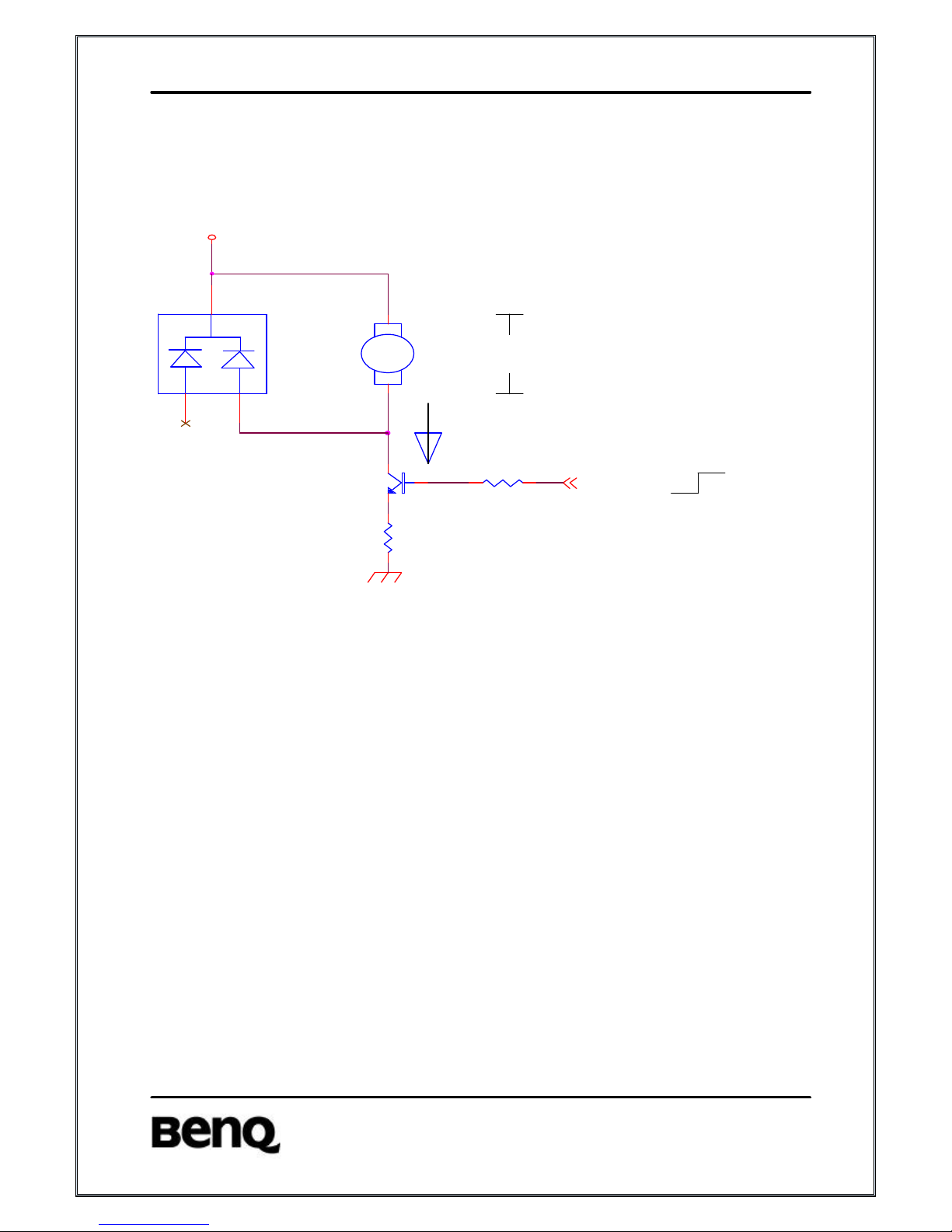
56D72 Vibrator & Buzzer
D14
T10
BQ4
R49
R46
On Side 2
IOVIBRATOR
R71
R45
BQ3
On Side 2
D14
T10
BU
U1.C2
U1.J3
VBAT
VBAT
Page 39

BenQ Rev 1.0
41
GND
VPP
I / O
VCC
RST
CLK
U3.D5
R4
U3.A2
U3.D4
C6
U2
R3U3.B4
C4R7
R8
C5
3V/5V
SIO5
SCLK5
SVDD
SRST5
1.6/3.2MHz
56D72 SIM Circuit
1.6/3.2MHz
Page 40

BenQ Rev 1.0
42
56D72 Keypad and LEDs
D5
D6
D7
D8
D9 D10
D11
D12
ROW0
U1.A4
ROW1
U1.B4
ROW2
U1.D4
U1.B3
ROW3
U1.A6
COL0
U1.A5
COL1
COL2
U1.B5
COL3
U1.D5
COL4
U1.E5
ROW4
U1.A2
D2
PWON
U3.B10
D3
D4
D13
R40
R35
BQ2
U7.6
R34
VBATBB
1.9V
LCD
Backlight
1.9V
On Side 1
On Side 1
Page 41

BenQ Rev 1.0
43
56D72 LCD Circuit
VR2
I2C_SCL
C32
R27
C34
C50
C33
C51
NRSTOUT
I2C_SDA
U1.K11
10 9 8 7
6
5 4
3
2 1
RN3.1 / U1.C4
RN3.2 / U1.F4
2.9V
7.6V
2.9V
400KHz
J2
Page 42

BenQ Rev 1.0
44
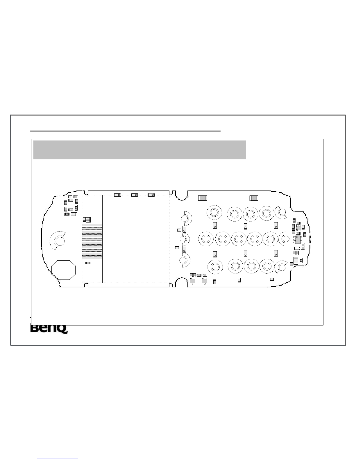
△ Radio Frequency function Descriptions (Top Side)
Page 43

BenQ Rev 1.0
45
Bottom Side
Page 44

BenQ Rev 1.0
46
Tx Flow Chart
T/R Switch For TX
EGSM:880.2∼914.8MHz
DCS:1712.2∼1786.8MHz
(LMC33-07A0533A)
DCS:3604.4~3753.6 MHz
GSM:3700.8~3839.2 MHz
RFVCO
(UCVE4X307)
Dual Band PA
Tx
EGSM:880.2∼914.8MHz
DCS:1712.2∼1786.8MHz
(CX77301)
RF Synthesizer
(HD 155141TF)
Mixer with RF
(HD155141TF)
Loop
Filter
Phase
Dectector
I/Q
Modulator
I
Q
DCS: 360/368MHz
GSM: 360/368MHz
IFVCO
(HD155141TF)
IF Synthesizer
(HD 155141TF)
DCS/4=90/92MHz
EGSM/8=45/46MHz
TX VCO
EGSM: 880.2∼914.8 MHz
DCS:1712.2~1786.8 MHz
(ENFVF382S12)
HD155141TF
Page 45

BenQ Rev 1.0
47
Rx Flow Chart
T/R Switch For RX
EGSM:925.2∼959.8MHz
DCS:1805.2∼1879.8MHz
(LMC33-07A0533A)
DCS:3610.4~3759.6 MHz
EGSM:3700.8~3839.2 MHz
RFVCO
(UCVE4X307)
DUAL SAW FILTER
EGSM:925.2∼959.8MHz
(B7710)
DCS:1805.2∼1879.8MHz
(SAFSD1G84CB0T00)
Mixer with RF
(HD155141TF)
DC Offset
Cancellation
(HD155141TF)
I
Q
LNA
(HD155141TF)
RF Synthesizer
(HD 155141TF)
Page 46

BenQ Rev 1.0
48
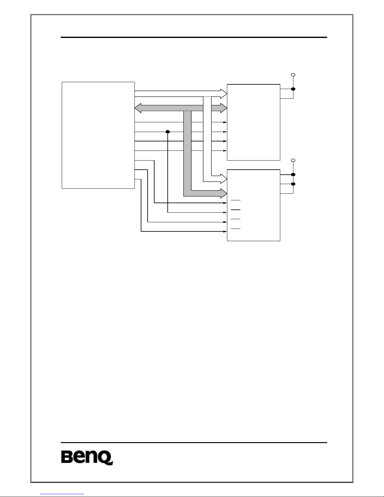
Tx Block Diagram
Dual Band PA
T/R
Switch
Charge
Pump
PFD
2
QTxP
QTxN
ITxP
ITxN
EGSM : 45 MHz
DCS : 90 MHz
TX EGSM : 880.2~ 914.8 MHz
DCS : 1712.2~1786.8 MHz
Loop Filter
2
DCS:3604.4~3753.6 MHz
EGSM:3700.8~3839.2 MHz
RFVCO
RF
Synth
IFVCO
I&Q Mod
90
0
Shift(1/2)
IF
Synth
2
2
DCS
EGSM
DCS
EGSM
DCS:1802.2~1876.8 MHz
EGSM: 925.2~959.8 MHz
DCS:360/368 MHz
EGSM: 360/368 MHz
DCS : 90/92 MHz
EGSM : 45/46 MHz
Page 47

BenQ Rev 1.0
49
Rx Block Diagram
T/R
Switch
90
0
90
0
90
0
90
0
QRxP
QRxN
IRxP
IRxN
EGSM LNA
DCS LNA
EGSM: 925.2~959.8 MHz
DCS:1805.2~1879.8 MHz
2
DCS:3610.4~3759.6 MHz
EGSM:3700.8~3839.2 MHz
RFVCO
Shift(1/2)
Shift(1/2)
ADC/DAC & Control Logic for DC Offset Cancellation
RF
Synth
DCS:
1805.2~1879.8 MHz
EGSM:
1850.4~1919.6 MHz
Page 48

BenQ Rev 1.0
50
U75
U73
U67
U66
U71
C704
D
3
U61
U65
U85
U63
U64
U74
RF circuit element placement
Page 49

BenQ Rev 1.0
51
U75
U73
U67
U66
U71
C704
D
3
U61
U65
U85
U63
U64
U74
EGSM 900 Receive Signal Path Diagram
U72
CW Wave
CH 62 947.46MHz
-50dBm
-53dBm
-54dBm
-63dBm
-63dBm
Phone setting
+:continuous RX mode
ARFCN:62
BB PGC Gain value:3
IF PGC Gain value:60
LNA turned off:n
Legend:
chip inductor
chip capacitor
chip resistor
Vpp = 0.9V for
RFin=-60dBm
-3dBm
1.66V
2.84V
Page 50

BenQ Rev 1.0
52
U75
U73
U67
U66
U71
C704
D
3
U61
U65
U85
U63
U64
U74
CW Wave
CH 700
1842.86MHz
-50dBm
-53dBm
-56dBm
-63dBm
-63dBm
Phone setting
+:continuous RX
modeARFCN:700
BB PGC Gain value:3
IF PGC Gain value: 60
LNA turned off :n
Legend:
chip inductor
chip capacitor
chip resistor
Vpp = 0.7V for
RFin = -60dBm
-3dBm
1.18V
2.84V
DCS 1800 Receive Signal Path Diagram
Page 51

BenQ Rev 1.0
53
U75
U73
U67
U66
U71
C704
D
3
U61
U65
U85
U63
U64
U74
DCS 1800 Transmit Signal Path Diagram
U72
CH 700
1747.8MHz
27dBm
C806
0V
L606
C622
DC 1.18V
AC 0.46Vpp
1747.8
MHz
1747.8MHz
6dBm
C714
3675.6MHz
-1dBm
0V
1.1V
0V
2.8V
0V
2.8V
C621
26MHz
C709
1748.8MHz
24dBm
1747.8MHz
28dBm
1.6V
0V
1.4V
360MHz
-4dBm
DC 1.18V
AC 0.46Vpp
DC 1.18V
AC 0.46Vpp
1.8V
1.4V
Phone setting
RF toolkit mode
CH 700 : ARFCN
Power Supply Setting : 3.8V
Spectrum Analyzer Trace : Max Hold Mode
800 : scaling factor
6 : Data pattern =>random data=>TSC=5
Legend:
chip inductor
chip capacitor
chip resistor
3.8V
Page 52

BenQ Rev 1.0
54
U75
U73
U67
U66
U71
C704
D
3
U61
U65
U85
U63
U64
U74
EGSM 900 Transmit Signal Path Diagram
U72
CH 62
902.4MHz
31dBm
C806
0V
L606
C622
DC 1.18V
AC 0.46Vpp
902.4MHz
5dBm
C715
3693.6MHz
-2dBm
0V
1.6V
0V
2.8V
0V
2.8V
C621
26MHz
C709
902.4MHz
27dBm
1.6V
0V
1.3V
368MHz
-5dBm
DC 1.18V
AC 0.46Vpp
DC 1.4V
AC 0.7Vpp
2V
1.9V
902.4MHz
28dBm
6.5dBm
Phone setting
RF toolkit mode
CH 62 : ARFCN
Power Supply Setting : 3.8V
Spectrum Analyzer Trace : Max Hold Mode
Legend:
chip inductor
chip capacitor
chip resistor
800 : scaling factor
6 : Data pattern =>random data=>TSC=5
3.8V
Page 53

BenQ Rev 1.0
55
1.T/R switch:
U75 is a front-end switch device for GSM/DCS.
These devices include 1 diplexer + 2 switches + 2 LPFs. The below
table shows the three operating mode.
Mode Vc1 (pin 2) Vc2 (pin 11)
GSM TX L H
DCS TX H L
GSM Rx and DCS
Rx
L L
These four control signals are generated from U73 Dual Buffer, which
controlled by GSM_T/R(U1 Pin B10) DCS_T/R(U1 pin E9).
2.PA and power control circuit:
PA (U71) is control by signal BS and APC (U74 Pin7). APC is
generated from U74 (Operational Amplifier), which controlled by RAMP
signal (U3 pin 47). The power control loop is a current sensor. U74
works as the error amplifier. It can compare the RAMP signal and
feedback signal from R702 then amplify the error part to drive PA. U86
is a switch for power saving. Please refer to TX signal path chart for
detailed signal waveform. Please refer to TX signal path chart for
detailed signal waveform.
3.Transceiver:
U61 is the transceiver.
A>.Receiver Operation
The receiver employs a direct-conversion architecture. The
incoming RF signals pass via a suitable front-end filter into the
balanced LNA and a pair of Gilbert Cell mixers. The mixers convert the
RF signal directly down to baseband frequencies. The I/Q local
oscillator signals for the mixers are derived from a 3.6~3.84GHz RFLO,
divided down by high-speed BiCMOS flip-flops. The receiver has 2
separate front-end blocks, optimized for 900MHz and 1.8GHz operation
respectively. Each front-end block has 3 discrete gain settings. These
settings allow the signal levels in the receiver to be optimized,
particularly under high signal conditions. The I/Q baseband lowpass
filters and programmable gain amplifiers follow the mixer. The
Page 54

BenQ Rev 1.0
56
baseband filtering is distributed in the PGA and comprises a single R/C
low-pass section and 2 second order Butterworth filters. The majority of
the baseband filtering is implemented on-chip. Each 3 stage PGA is DC
coupled and has a gain range. The base-band PGA has 2dB gain steps
and 90dB control range. The baseband PGA includes a DC offset
cancellation system.
The signal is then down converted by a demodulator to I and Q.
B>.Transmitter Operation
The transmitter chain converts differential IQ baseband signals to a
suitable format for transmission by a power amplifier.
The common mode voltage range of the modulator inputs is 0.9V to
1.4V and they have 1.25V differential swing. The modulator circuit uses
double-balanced mixer for the I and Q paths. The Local signals are
generated by dividing the IFLO signals by 8 for GSM, and dividing IFLO
signals by 4 for DCS, and then passed to the modulator through a
phase splitter / shifter. The IF signals generated are then summed to
produce a single modulated IF signal which is amplified and fed into the
offset PLL block.
Within the offset PLL block there are a down converter, a phase
comparator and a VCO driver. The down converter mixes the first local
signal and the TXVCO (U65) signal to create a reference local signal
for use in the offset PLL circuit. The phase comparator and the VCO
driver generate an error current, which is proportional to the phase
differential between the reference IF and the modulated IF signals. This
current is used in a second order loop filter to generate a voltage, which
in turn modulates the TXVCO.
4. Synthesizer:
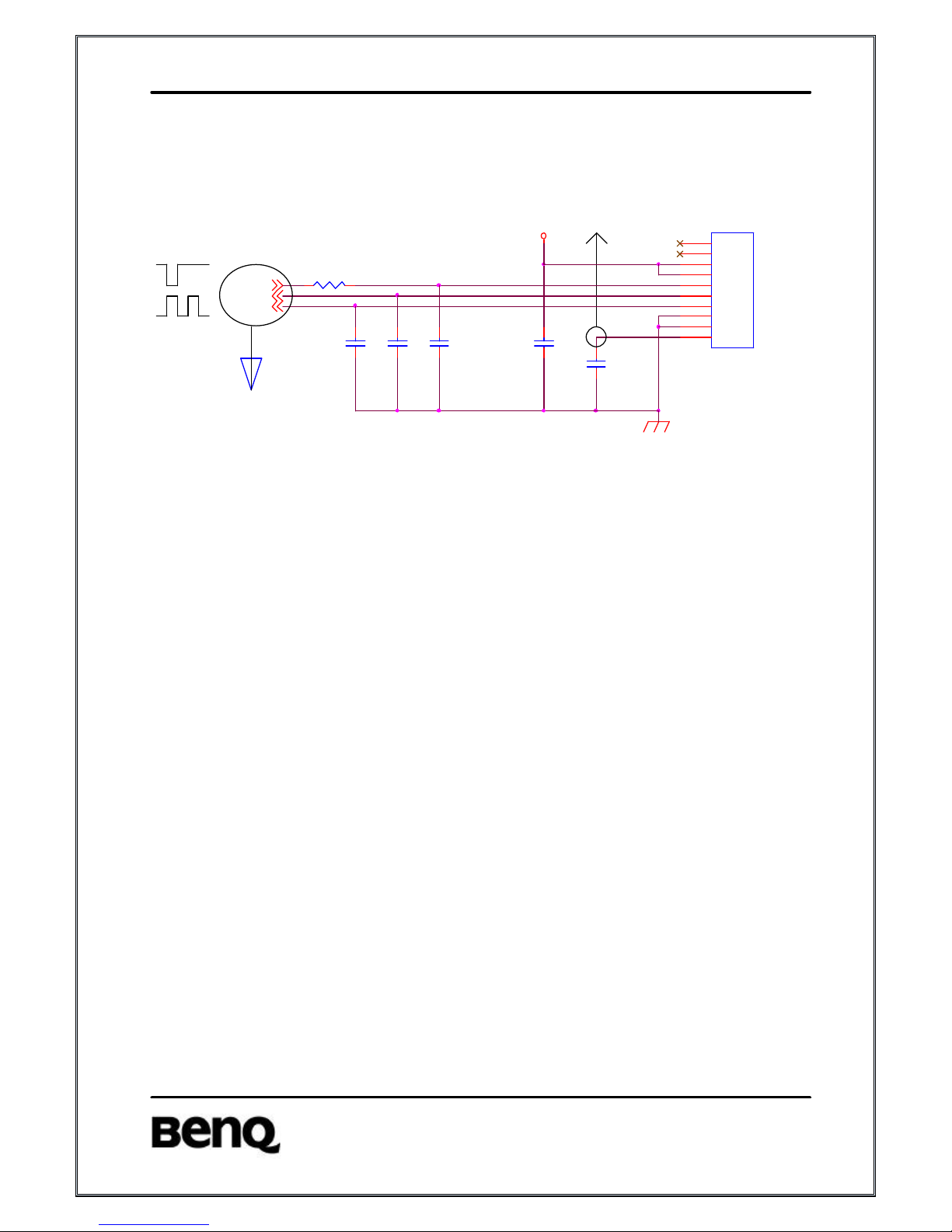
A>.TCVCXO
U85 is a TCVCXO module which providing RF system clock (26
MHz). The 13MHz generated by dividing the 26 MHz by 2 provide
Baseband system clock. U3 (Pin F8) can fine tune the clock frequency
by AFC signal (U85 Pin1).
B>.RF VCO
Page 55

BenQ Rev 1.0
57
U63 is a RF VCO module. The frequency band is 3610∼3840 MHz
for GSM / DCS TX / RX. The output frequency can be controlled by
U61 pin 43,44.
C>.IF VCO
IF VCO consists of U61 pin 32、33, D601、D602(varactor) and other
RLCs. The operating frequency is 360 MHz, and 368MHz. The output
frequency is controlled by U61 pin 34.
5.Regulator
U90 is the Dual regulator for RF circuit. The first regulator (pin 1)
provides transceiver 2.85V and TXVCO (U65) 2.85V through Q700
pin6 which is a switch for power saving. The second regulator (pin 6)
provides synthesizer of transmitter and RFVCO (2.85V) through Q700
pin3. All the Dual regulators can be shut down simultaneously by set
TCXOEN signal (U1 pin E11).
Table A
Receiver Troubleshooting and Repair Chart
Rx Symptom Probable Cause
Verification and Remedy
1. Portable
telephone
exhibits poor
reception
and/or erratic
operation
(such as calls
a) Antenna
assembly is
defective.
1. Check to make sure that
the antenna is properly
touched to the telephone
Main Board pad. If not,
substitute a known good
antenna assembly.
2. If the fault is still present,
proceed to b.
Page 56

BenQ Rev 1.0
58
frequently
dropping,
weak and/or
distorted
audio, etc.).
b) Defective or
misplaced
telephone Main
Board.
1. Check for appropriate
frequencies and power
level gains/losses in the Rx
path.
2. Replace malfunctioning
components if listed in
parts list. Likely fail
components are:U75,
C608, C609, L601, L602,
L603, and L604.
3. If parts replacement
doesn’t correct the fault,
replace the SAW filter U66,
U67, or transceiver U61.
Table B
Transmitter Troubleshooting and Repair Chart
Tx Symptom Probable Cause Verification and Remedy
a) Microphone
connections to
Main Board
defective.
1. Check connections and
if OK, proceed to b.
1.Transmit audio
is weak,
(usually
indicated by
called parties
complaining of
difficulty in
hearing voice
from portable
phone).
b) Microphone
defective.
1. Substitute a known
good microphone.
2. Place a call and Verify
improvement in portable
transmit signal as heard
by called party. If good,
re-assemble portable
with new microphone
3. If microphone is not at
fault, re-install original
microphone and
proceed to c.
Page 57

BenQ Rev 1.0
59
c) Main Board
assembly
defective.
1. Replace Main Board
Assembly.
2. If Main Board Assembly
is at fault, examine for
improper solder and
connections.
Download
Introduction:
This document describes all the functions in service DMtool.
△ System requirements and setup:
A. Minimum requirement:
Operation system: Win95/ Win98 / WinNT / Win2000.
CPU: Pentium 233 Mhz or higher.
Hard Disk: Free 10MB space.
Memory: 64MB RAM.
Input Device: Keyboard and mouse
B. Calibration requirement:
1.Instrument for calibration Hp8922M GSM/DCS/PCS MS Test Set
Hp8960 GSM/DCS/PCS RF Interface
2.GPIB interface card and cable For RF calibration
3.Power Supplies:
HpE3631,Hp66332A,Hp66311,Hp66111,Hp66309
4.Communication cables Rs232 and Acer Downloader
5.RF Cable 50 ohm cable for RF calibration.
6.Dummy battery For RF and battery calibration.
C. Setup in Windows:
Page 58

BenQ Rev 1.0
60
In Windows 95/98/NT/2000, extract the Dmtool compress files to
any temporary directory. It will create DISK1 this subdirectory. Please
go into the DISK1 and double click the setup.exe. The Install shield
will auto setup the Dmtool in your operating system.
Some necessary files are listed below :
Fixed Items:
===============================
(1) DMtool.exe (main application )
(2) DL.dll (the dll for download)
(3) CALDL.dll (the dll for calibration)
(4) E2pMmi.dll (the dll for read/write e2p and mmitest)
(5) AtStCom.dll (the dll for animation and melody download)
(6) r_flash_xx.mot (Rs232 boot code file)
(7) dmtool.hlp, dmtool.cnt (dmtool help file)
(8) AutocalMarch.cfg (auto-calibration parameter reference file)
Volatile Items:
===============================
The files you gotten may differ from the files listed below as the
result of software upgraded for handsets. When the software of
handsets release, you will get a handset program file and an eeprom
database file.
(9) mh1060.bin (eeprom database file, its file extension name must
be “bin”
(10) mh106010.mot (handset program file, its file extension name
must be “mot”
Page 59

BenQ Rev 1.0
61
△ Function descriptions:
There are several windows (views) in the DMtool application.
Each view performs a special function.
A. Download:
Before you start a RS232 download, you must select a flash-load
program file by pressing down the “Flash File” button or “Set Flash
File” submenu button in “File” menu. Then you must select the
correct com port in “Option” menu. When the Dmtool application
setup completed, the default boot code will be assigned. You don’t
need to change the boot code yourself. You can change boot code
by “Boot File” button or “Set Boot Code File” submenu button in
“File” menu. If you assigned incorrect flash or boot code file, you
may still encounter errors.
Before press “Download” button to start a RS232 download
process, you must power off the handset. When the string “Wait for
target ready” appears, power on the handset. Then the download
process starts. It will take about 5 minutes for completing the
download.
After undergoing a completed download process, the Dmtool will
auto trigger a Set E2P Default dialog to execute set e2p default.
There are two option, “Set E2P Default” or “Set E2P Default and
Phone Book Initialize” in this dialog. You must select “Set E2p
Default and Phone Book Initialize” and click the “OK” button. After
the “Wait for target ready” message appears, power on the handset.
If the handset receive the set e2p command form dmtool, it will start
to execute set e2p command and send the ack message to dmtool.
When the dmtool received the ack from handset it will display the
message “Waiting for target Acknowledgment …”. If the handset
complete the set e2p command, it send the ack to dmtool. When the
dmtool receive the ack message, it will display “Set e2p command
success” message.
Remark:
1. It must be emphasized that never stop or remove the power
supply (battery) when your handset is downloading the block 0
Page 60

BenQ Rev 1.0
62
and block 1 program codes . It is writing critical boot codes at
this time. If you terminate the download process at this moment,
this handset not only can’t power on but also can’t re-download
again. In this case , the only solution is using a special “Jtag
interface and cable” to do a low-level download.
2. When the new vendor flash used in handset, the boot code
r_flash_xxx.mot need upgrade to new version which support
new vendor flash.
B. Set E2P:
There are several sub-options for this function. You can select these
option from “Set E2p Mode” submenu in “Option” menu. You can see
which set e2p mode you select current in the status bar (in the
right-bottom) of the window. To execute those options, first power off
the handset and click this “Set E2p” button. After the “Wait for target
ready” message appears, power on the handset. Details for each
sub-options are listed below.
(1).Set EEPROM default will set a part of contents in EERPOM to
factory default value. Phone books and calibration data won’t be
reset in this operation.
(2).Set EEPROM Default Phone books initialize is similar to Set
EEPROM default, but this option will erase all phone book data in
EEPROM.
C. Read/Write FlexOption:
”Flex option” is used for modifying the handset’s flex option settings.
Changing those options are straightforward, just click the individual
enable/disable check button of every tree-item. The procedure to
Read/Write FlexOption is:
(1).Set baud rate 115200 and select com port then connect RS232
communication.
(2).Turn on the handset.
(3).Check the database file are the same as software version. You
can assign database file from menu “File” à “Set Database
File”. You can verify software version by keypress “*#300#” in
handset.
(4).Click “Read Flex Option” to read flex option from handset.
Page 61

BenQ Rev 1.0
63
(5).Select the feature you want enable/disable by click check button
in option tree-item.
(6).Click “Write Flex Option” to write flex option to handset.
D. Calibration:
(1).calibration connect cable:
PS:
1. In some calibration instrument, the RF output of GSM and
DCS are different, so you must calibrate GSM and DCS each
other.
2. If you have no connector with power supply and Acer
downloader, you can get a travel charger and cut it, then
divide the positive and negative electrode to connect into
power supply.
(2). Calibration Item:
2-1.Configuration file:
The auto-calibration configure file contents some
optimal value for some object in handset and some
parameters dependent on calibration device and handset.
u
v
Calibration
Instrument
PC
RF output
Power
Supply
Acer
downloader
GPIB
Com
GPIB
GPIB
Rs232
RF Cable
Power lines
Downloader cable
Dummy battery
u w x
GSM I/O
Power
Handset
Page 62

BenQ Rev 1.0
64
2-2.Auto-Power-Control:
If the flag is TRUE and the power supply is a supported
type (please refer to System Requirement
) , the calibration
will start automatically, or you must operate it manually.
2-3.Set Ramping Default:
Some measurement instruments do not support ramping
calibration, you can set the ramping table by default values.
2-4.HW Version:
The hardware version of the target handset. It combined
with major and minor hardware version. The major hardware
version is indicates the type of PA, and the minor hardware
version indicates the type of baseband or others.
Major version 1.x – Conexant PA
Major version 2.x -- Hitachi PA
2-5.PA Type Selection:
There are two kinds of PA, Conexant PA and Hitachi
PA. Before you start to calibrate, you must select the correct
PA type.
2-6.Auto-calibration selection:
Choose the items that you want to calibrate when
running auto-calibration function.
AFC: Frequency. (Before calibrate AFC, you must select
AGC Item)
AGC: RxGain
APC: TxPower
ADC: Battery is for battery A/D converter calibration
ARC: Ramping table calibration.
2-7.Band selection: Choose the frequency band for calibration.
GSM900
DCS1800
E. Start calibration:
Before start calibration you must check the following things:
(1) Change your battery to dummy battery.
(2) Check connect cable is OK?
(3) Check GPIB interface is OK?
(4) Power on power supply and set it to 3.8 V
Page 63

BenQ Rev 1.0
65
Before Click the “Auto-Calibration” button, make sure all listed
items are done:
(1) Set the correct com port and baudrat in option menu
(2) Choose Auto-calibration configure file. When you set up the
program success, we had assigned the default configure file.
What you want to do is to check or set the value of the field
Board_Address to your GPIB0 primary address.
For example: Auto-calibration configure file [GPIB_DEVICE]
Board_Address=0 ç GPIB0 primary address.
(3) Check your target handset software version(you can input
*#300# int the keypad)And assign the correct database file
which dependent with the software version of target handset.
(4) Check your target handset hardware version(you can input
*#300# in the keypad). Then select your PA Type by your
hardware version. 1.0 for Conexant PA and 2.0 for Hitachi
PA. And input the hardware version of target handset in HW
Version field of window.
(5) Choose calibration items and frequency band in check box.
When all settings are done, just click the “Auto-Cal” button in
main window to start the calibration process.
(1) If the power supply is a supported type, the calibration will
start automatically, or you must operate it manually: Turn off
the power supply before the calibration start, and turn it on
immediately when the message Wait for target ready show
up. For details: If your power supply isn’t supported by
dmtool, then you must turn off the power supply (please refer
the figure of “Calibration Connect Cable” ), then the power
of target handset and Acer downloader will turn off. when the
message “Wait for target ready” show up, you must turn on
the power supply immediately. If your power supply is
supported by dmtool and you check up the Auto Power
Control check box, then the dmtool will auto do the all things
in the above.
Page 64

BenQ Rev 1.0
66
(2) If the DmTool receive the signal from target handset , then it
will start to identify calibration device, and show up Identify
Calibration device… message. If the calibration device
identified ok, then it will start the calibration.
(3) And then the dmtool will start auto calibrate the target handset
with calibration instrument, and receive the result messages
of calibration . You can see the result message of calibration
in the Calibration Window.
(4) Calibration Notes:
There are 5 options for auto-calibration:
AGC (RX)
AFC (Frequency error)
APC (TX)
ARC (Ramping)
ADC (Battery)
There is no correlation between AGC, APC, and ADC
options ,therefore you can make any combinations when calibrate
these options. However, AFC need some parameters gotten from
AGC, you must select AGC when you want to calibrate AFC.
Besides, GSM and DCS share the same parameters of AFC and
AFC will be calibrated only in GSM band, you should select GSM
band to calibrate AFC.
ARC requires some parameters gotten from APC, but these
parameters can be retrieved from the E2P memory in target
handset. Thus if you can guarantee these parameters are
well-setup, you can calibrate ARC only without APC. If you know
nothing about it, then calibrate both of them is a recommendation.
If your calibration instrument can only calibrate one band (GSM
or DCS) at a time, you have to pay more attention about the
combination of calibration options, recommended combinations are
list below:
(1). GSM band :
AGC, ADC ,and APC can be calibrated separately.
AGC+AFC
Page 65

BenQ Rev 1.0
67
APC+ARC
AGC+AFC+APC
AGC+AFC+APC+ARC
AGC+AFC+APC+ARC+ADC
(2). DCS band :
AGC, ADC, and APC can be calibrated separately.
APC+ARC
AGC+APC
AGC+APC+ARC
AGC+APC+ARC+ADC
If your calibration instrument can’t support ramping calibration, we
support Set Ramping default to set the ramping table to optimal
default value.
F. E2p Clone:
”E2p Clone” is used for duplicating the data in the handset’s
EEPROM. It backup the Network-Lock, handset-feature settings, and
phone book records to PC and enable users to restore them to
handsets latter. The procedure to Read/Write FlexOption is:
(1)Set baud rate 115200 and select com port then connect RS232
communication.
(2)Turn on the handset.
(3)Check the database file are the same as software version. You
can assign database file from menu “File” à “Set Database File”.
You can verify software version by keypress “*#300#” in handset.
(4)Select the e2p backup file and phonebook backup file.
(5)Click “Backup” to backup e2p and phonebook from handset to
file.
(6)Click “Restore” to restore e2p and phonebook from file to
handset.
△ FAQ:
1.How do I select a correct boot code file?
The boot code file plays an important role during a download
procedure. It takes care of programming flash ROM and is responsible
for data receiving/transmission. The boot code files for download vary
Page 66

BenQ Rev 1.0
68
as different MS models. For March model, it uses r_flash_xxx.mot.
When the new vendor flash used in handset, the boot code
r_flash_xxx.mot need upgrade to new version which support new
vendor flash. Users just need to click the “Boot File” button in Download
window or click the “Set Boot Code File” menu button in “File” menu to
select this file.
2. Why can’t I download/upgrade programs into the handset?
For RS232 download, verify the following procedures step by step:
1. Do you set the switch to left side in your downloader?
2. Do you assign a correct boot code file?
3. Do you select a correct COM port?
4. Dose the connection between the MS and PC setup properly?
5. Do you power off the MS before the download starts?
6. Do you power on the MS after the sentence “Wait for Target
ready…” appear?
7. Have you ever terminated a download process when it was
downloading the block 0 and 1 codes? If yes, then the boot-code
area of this handset has been corrupted and can’t use RS232
download.
3. Why can’t set e2p?
1. Do you select a correct COM port?
2. Dose the connection between the MS and PC setup properly?
3. Do you power off the MS before the Set E2p starts?
4. If the sentence “Wait for Target read…” dosen’t appear, it may be
some application occupied the com port now. Please terminate
that application and execute set e2p again.
Page 67

BenQ Rev 1.0
69
Disassembly
Introduction
Responsible care should be taken during the disassembly and
reassembly of the units in order to avoid damaging or stressing the
housing and internal components. Ensure that a properly grounded
high impedance conductive wrist strap is used while performing these
procedures on electronic units.
NOTE Many of the integrated circuit devices used in this equipment are
vulnerable to damage from static charges. Ensure that adequate static
protection is in place when handling, shipping, and servicing the internal
components of this equipment.
Recommended Tools
The following tools (or similar tools with the same functions) are
recommended for use during the disassembly and reassembly of the
phone.
• Anti-Static Mat (Ground Cord included)
• Anti-Static Wrist Strap
• Torque Screw Driver (T5 type, torque is set to 1.2kg-cm)
• Tweezers
Page 68

BenQ Rev 1.0
70
Disassembly Procedure
The following information describes the procedure for removing
and accessing various parts of the phone.
Front Case Removal
1. Turn off the telephone.
2. Slide down the bottom cover,
and remove the battery pack
from the Rear housing.
3. Remove the bottom cover and
nameplate from the rear housing.
4. Release the six screws and
remove them.
Page 69

BenQ Rev 1.0
71
5. Unclip the 2 snap fits from the left
and right hand sides of the unit and
separate the rear from the front
housing
Main Board Removal
1. Carefully separate the main
board from the front housing by
lifting it upwards.
2. Carefully use a tweezers to remove
the four corner of RF Shielding case.
3. Carefully use a tweezers to remove
the four corner of BB Shielding case.
Page 70

BenQ Rev 1.0
72
4. Place the main board facing
upwards on an anti-static mat.
5. Place a protection tape over
the LCD module.
NOTE Do not touch the LCD
module with your hands!
6. Remove the Keypad from the front
housing by lifting it upwards.
Assembly Procedure
Once the unit is disassembled and the repair is carried out, it then
becomes obvious that to assemble the unit, the procedure is the
Page 71

BenQ Rev 1.0
73
reverse of that previously completed for disassembly.
Troubleshooting
△ Level 1 ~level 2 repair
Symptom Probable Cause Verification and Remedy
a).Battery either
discharged or
defective.
1. Measure battery voltage. If the battery
voltage is <3.2V, recharge the battery
using the appropriate battery charger.
2.If the battery can’t be recharge, replace
the battery.
1.Unit
doesn’t turn
on
b).Shield case short
with components
1.Visually inspect the RF/BB shielding
case. If they become deformed , replace
the shielding case.
2.Keypad no
function.
Keypad bottom short 1.Disassembly to
replace the keypad metal
dome.
3.Buzzer no
function
Components shift 1.Disassembly to visually inspect the U13.
If the spring of the U13 becomes
deformed, replace the U13.
4.Vibrator no
function
Components shift 1.Disassembly to visually inspect the M1.
If
the spring of the M1 becomes deformed
and doesn’t contact well with PCB pads,
replace the M1.
5.Speaker
no function
Components shift 1.Disassembly to visually inspect the LS1.
If the spring of the M1 becomes
deformed and doesn’t contact well with
PCB pads, replace the LS1.
6.Micphone
no function
Components shift
1.Disassembly to visually inspect the X2. If
the cover of the X2 is not matched with
the micphone hole or micphone doesn’t
contact well with PCB pads, replace the
cover of the X2 or micphone.
7.Datacable
no function
Components are at
fault.
1.Measure voltage level if VR3 and
VR2B_SW voltage level are equal 2.9V.
Page 72

BenQ Rev 1.0
74
8.Can’t
charge
Battery or charger is
at fault
1. Use the correct battery and charger to
check the charge function.
2.If charging function is ok, the battery or
charger is illegal.
△ Level 3~ level 4 repair
Symptom Probable Cause Verification and Remedy
a) Battery either
discharged or
defective.
2. Measure battery voltage. If the battery
voltage is <3.2V, recharge the battery
using the appropriate battery charger.
3. If the battery can’t be recharge, replace
the battery.
4. If the battery is not at fault, proceed to
b.
b) Battery connector
open or misaligned.
1. Visually inspect the battery connectors
on both the battery pack and the unit.
2. Disassembly to check the battery
connectors if it misaligned or short with
the RF or Base-band shielding cases. If
necessary, replace either the battery or
battery connector.
3.
If the battery connectors are not at fault,
proceed to c.
1.Unit
doesn’t turn
on
c) Shield case short
with components
1. Visually inspect the RF/BB shielding
case. If they become deformed, replace
the shielding case.
2. If the shielding case are not at fault,
proceed to d.
Page 73

BenQ Rev 1.0
75
d) X1, R56, C1 or
C2
1. Use the power supply to supply the
VBAT voltage. Then, press the
power-on key. Visually inspect the
current of the handset used.
2. Measure the waveform of the R56.
3. If the waveform isn’t the 32KHz clock,
replace the C3 and R2.
4. If they are not at fault, proceed to e.
e) C3 or R2 is at
fault.
1. Measure the waveform of the R2.
2. If the waveform isn’t the 13MHz clock,
replace the X1, R56, C1 or C2.
3. If they are not at fault, proceed to f.
f) U3 is at fault.
1. If the current is under 100mA when
power on, check the VR1 (2.5V), VR2
(2.9V), VR2B (2.9V), and VR3 (2.9V)
voltage.
2. If they are not correct, maybe the U3 is
at fault. Replace the U3.
a) LCD module is at
fault
1.
Disassembly to visually inspect the LCD
module. If the glass is break on the
LCD, replace the LCD module.
2. If the LCD module is not brea
k, proceed
to b
2.LCD no
display.
b) LCD module has
no power.
1. Visually inspect the C34 or R27 is still
on the board. If no, replace the C34 or
R27.
2. Measure the voltage of C34. If it is not
about 8V, the LCD driver IC is failed on
the LCD module. Replace the LCD
module.
3. If
the LCD module is not break, proceed
to c
Page 74

BenQ Rev 1.0
76
c) U1 is at fault
1. Power on the handset. Then measure
the waveforms of the J2.6, J2.4 and
J2.5 pins.
2. If the J2.6 pin is always low or the other
two pins (J2.4 and J2.5) are no data,
the U1 is at fault. Replace the U1.
3.Keypad no
function.
Keypad bottom short Disassembly to replace the keypad metal
dome.
a) Components shift
1. Disassembly to visually inspect the U7,
R34, BQ2, R40, R35. If any component
is shifted, replace the components.
2. If they are not shifted, proceed to b
b) U1 is at fault
1. Measure the waveform of the U7.2. If
the U7.2 doesn’t output any signal when
LED function is executed, U1 is at fault.
2. If it is not at fault, proceed to c.
4.LED no
display
c) Other
components are at
fault.
1. Measure the waveform of the U7.6,
BQ2.2, and BQ2.3 when LED function
is executed.
2. If any pin is no signal, replace the
component relative to that pin.
a) Components shift
1. Disassembly to visually inspect the
U13. If the spring of the U13 becomes
deformed, replace the U13.
2. Visually inspect the R48, BQ3, R45,
and R71. If any component is shifted,
replace the components.
3. If they are not shifted, proceed to b
5.Buzzer no
function
b) U1 is at fault
1. Measure the waveform of the D16.1. If
the D16.1 doesn’t output any signal
w
hen Buzzer function is executed, U1 is
at fault.
2. If it is not at fault, proceed to c.
Page 75

BenQ Rev 1.0
77
c) Other
components are at
fault.
1. Measure the waveform of the BQ3.3,
BQ3.2, and BQ3.1 when Buzzer
function is executed.
2. If any pin is no signal, replace the
component relative to that pin.
a) Components shift
1. Disassembly to visually inspect the M1.
If the spring of the M1 becomes
deformed and doesn’t contact well with
PCB pads, replace the M1.
2. Visually inspect the R46, BQ4, and
R49. If any component is shifted,
replace the components.
3. If they are not shifted, proceed to b
b) U1 is at fault
1. Measure the waveform of the R46. If
the R46 pin doesn’t output any signal
when Vibrator function is executed, U1
is at fault.
2. If it is not at fault, proceed to c.
6.Vibrator no
function
c) Other
components are at
fault.
1. Measure the waveform of the BQ4.3,
BQ4.2, and BQ4.1 when Vibrator
function is executed.
2. If any pin is no signal, replace the
component relative to that pin.
a) Components shift
1. Disassembly to
visually inspect the LS1.
If the spring of the M1 becomes
deformed and doesn’t contact well with
PCB pads, replace the LS1.
2. Visually inspect the R73, BL2, BL3 and
R74. If any component isn’t contacted
well, replace the components.
3. If they are not shifted, proceed to b
7.Speaker
no function
b) U3 is at fault
1. Measure the waveforms of the R73 and
R74. If the R73 or R74 pins don’t output
any signal when speaker function is
executed, U3 is at fault.
Page 76

BenQ Rev 1.0
78
a) Components shift
1. Disassembly to visually inspect the X2.
If the cover of the X2 is not matched
with the micphone hole or micphone
doesn’t contact well with PCB pads,
replace the cover of the X2 or
micphone.
2. Visually inspect the R50, R51, C44,
C45, R43, R44, R47, C42, C43, C53,
C54 and U14. If any component isn’t
contacted well, replace the components.
3. If they are not shifted, proceed to b
b) U3 is at fault
1. Measure the waveforms of the R50,
R51, and R43. If the R50 or R51 pins
don’t output any signal or Micbias
voltage level is not equal 2~2.5V when
micphone function is executed, U3 is at
fault.
2. If it is not at fault, proceed to c.
8.Micphone
no function
c) Other
components are at
fault.
1. Measure the waveforms of U14.5,
U14.1, U14.4 and U14.3 when
micphone function is executed.
2. If any pin is no signal, replace the U14.
9.Handfree
no function
a) Components shift
1. Disassembly to visually inspect the J3.
If audio jack (J3) pins don’t contact well
with PCB pads, solder the pins and
pads together.
2. Visually inspect the R72, R32, U9, U8,
U10, R36, BL1, R41, C38, R38, R37,
C37 and J4. If any component isn’t
contacted well, replace the components.
3. If they are not shifted, proceed to b
Page 77

BenQ Rev 1.0
79
b) U3 is at fault
1. Measure voltage level if VR3 and
VR2B_SW voltage level are equal 2.9V.
2. Measure the waveforms of the BL1,
R41, and J4. If the BL1 or R41 pins
don’t output any signal when handfree
function is executed, U3 is at fault.
3. If it is not at fault, proceed to c.
c) Other
components are at
fault.
1. When handfree is plugged in,
IO13ACCIN detect 0V. Then,
IO3DATA_HP_SEL outputs high level,
U8.1 pin connects to U8.4 pin and
U10.1 pin connects to U10.4 pin. If not,
maybe the U8 and U10 are at fault.
Replace the U8 or U10.
2. After IO3DATA_HP_SEL outputs high
level, measure the waveform of the
U10.4 pin. If its voltage level doesn’t
drop to 1 ~ 2.6V and the voltage of the
U3.C6 pin isn’t equal to 0.5 ~ 1.3V, test
it again by another handfree. If handfree
is still no function, U9, R37, R38, R6 or
R9 is at fault. Visually inspect the
components. If any component isn’t
contacted well or wrong, replace the
components.
3. Measure the waveforms of U9.5, U9.1,
U9.4 and U9.3 when handfree function
is executed.
4. If any pin is no signal, replace the U9.
Page 78

BenQ Rev 1.0
80
a) Components shift
1. Disassembly to visually inspect the J3.
If audio jack (J3) pins don’t contact well
with PCB pads, solder the pins and
pads together.
2. Visually inspect the R72, R32, U9, U8,
U10, R36, BL1, R41, C38, R38, R37,
C37 and J4. If any component isn’t
contacted well, replace the components.
3. If they are not shifted, proceed to b
10.Datacable
no function
b) Components are
at fault.
1. Measure voltage level if VR3 and
VR2B_SW voltage level are equal 2.9V.
2. When datacable is plugged in,
IO13ACCIN detect 0V. Then,
IO3DATA_HP_SEL outputs high level
about 1 ~ 2 sec, and switches to low
level. U8.3 pin connects to U8.4 pin and
U10.
3 pin connects to U10.4 pin. Check
if the U8.3 and U8.4 pins are short. If
not, maybe the U8 is at fault. Replace
the U8.
3. Check if the U10.3 and U10.4 pins are
short. If not, maybe the U10 is at fault.
Replace the U10.
4. After IO3DATA_HP_SEL outputs low
level, measure the waveform of the
U10.4 pin. If its voltage level isn’t equal
to 2.7 ~ 2.9V, maybe U9 is at fault. If U9
isn’t contacted well or wrong, replace
the component.
5. Measure the voltage of the U3.C6. If it
isn’t equal to 1.35 ~ 1.45V, maybe the
R6 or R9 is at fault. Check their voltage
value and replace the components.
6. If it is not at fault, proceed to c.
Page 79

BenQ Rev 1.0
81
c) U1 is at fault
1. Measure the waveforms of U8.3 and
U10.3 when datacable function is
executed.
2. If any pin is no signal, maybe U1 is at
fault then replace the U1.
a) Components shift
1.
Visually inspect the U2. If the pins of the
SIM socket is at fault, Disassembly to
replace the U2.
2. Disassembly to visually inspect the R8,
R7, C5, C8, R4, C4 and R13. If any
component isn’t contacted well, replace
the components.
3. If they are not shifted, proceed to b
12. Can’t
find SIM
b) Components are
at fault.
1. Plug in the SIM card to power on the
handset and measure the voltage of the
TPSIM1. If it isn’t equal to 3V or 5V,
check the R8 and replace it.
2. If R8 is ok but TPSIM1 is still no
voltage, proceed to c.
3. Measure the voltage of the TPSIM4 if it
goes to high about 3V or 5V. If not,
check the R7 and replace it.
4. If R7 is ok but TPSIM4 is still no
voltage, proceed to c.
5. Measure the voltage of the TPSIM2 if it
output a clock about 3V or 5V. If not,
check the R4 and replace it.
6. If R4 is ok but TPSIM4 is still no
voltage, proceed to c.
7. Measure the voltage of the TPSIM3 if it
goes to high about 3V or 5V. If not,
proceed to c.
Page 80

BenQ Rev 1.0
82
c) U3 or U1 is at
fault
1. If check the b steps and the TPSIM1,
TPSIM2, TPSIM3 or TPSIM4 is still no
signal, maybe the U3 or U1 is at fault.
2. Replace the U3 then re-check the step
b.
3. If it is still no signal, replace the U1.
a) Battery or charger
is at fault
2. Use the correct battery and charger to
check the charge function.
3. If charging function is ok, the battery or
charger is illegal.
4. If it still can’t charge, proceed to b
13. Can’t
charge
b) Components shift
5. Disassembly to visually inspect the J1.
If the pins of the power jack (J1) aren’t
contacted well with the pads of the
PCB, re-solder the pins.
6. Visually inspect the R60, C55, F1, R68,
R62, R63, R65, C47, R70, R64, U16,
U17, D1, R24, D15, C48, R66, R67 and
U18. If any component isn’t contacted
well, replace the components.
7. Visually inspect the polarity of the U17,
D1 and D15. If any component is
wrong, replace the component.
8. Check the F1. If it is open, replace the
F1.
9. If they are not wrong, proceed to c
Page 81

BenQ Rev 1.0
83
c) Peripheral
components for
charging are at fault.
1. Use dummy battery to check the
charging function. JP1.4 connected to
V+ (3.6V) of the power supply. JP1.1
connected to V- (GND) of the power
supply. JP1.3 connected to a resistor
(10K ohm) to ground. JP1.2 connected
to a resistor (47 ohm) to 1.2V of the
power supply.
2. Plugged in the charger then check the
voltage of the CHARGERIN pin and
U17.5 pin. If their voltage isn’t the same
about 4~6V, R68 is at fault. Replace the
R68.
3. Check the voltage of the U16.2 if it is
under 0.6V. If not, check the resistor
value of the R62 and R65. If anything is
wrong, replace the components.
4. Check the voltage of the U16.5 if it is
above 3V and the voltage of the U17.1
if it is under 0.6V. If not, maybe U16 is
at fault. Replace the U16.
5. Check the voltages of the U17.2 and
U17.4 if their voltages are above 4V. If
not, ma ybe U17 is at fault. Replace the
U17.
6. Check the voltage of the D1.2 if it is
above 4V. If not, maybe D1 is at fault.
Replace the D1.
7. Measure the current flowing across the
R24. If not, maybe R24 is at fault.
Replace the R24.
8. If they are not wrong, proceed to d
Page 82

BenQ Rev 1.0
84
d) U3 is at fault
1. When the charger is plugged in, the
voltage of the VCHG pin is 4~6V. And
when charging, the ICTL pin will
high/low to control charging pulse.
2. If not, maybe U3 is at fault. Replace the
U3.
Symptom Probable Cause Verification and Remedy
a) Battery either
discharged or
defective.
5. Measure battery voltage. If the battery
voltage is <3.2V, recharge the battery
using the appropriate battery charger.
6. If the battery can’t be recharge, replace
the battery.
7. If the battery is not at fault, proceed to
b.
b) Battery connector
open or misaligned.
4. Visually inspect the battery connectors
on both the battery pack and the unit.
5. Disassembly to check the battery
connectors if it misaligned or short with
the RF or Base-band shielding cases. If
necessary, replace either the battery or
battery connector.
6.
If the battery connectors are not at fault,
proceed to c.
c) Shield case short
with components
3. Visually inspect the RF/BB shielding
case. If they become deformed, replace
the shielding case.
4. If the shielding case are not at fault,
proceed to d.
1.Unit
doesn’t turn
on
d) X1, R56, C1 or
C2
5. Use the power supply to supply the
VBAT voltage. Then, press the
power-on key. Visually inspect the
current of the handset used.
6. Measure the waveform of the R56.
7. If the waveform isn’t the 32KHz clock,
replace the C3 and R2.
8. If they are not at fault, proceed to e.
Page 83

BenQ Rev 1.0
85
e) C3 or R2 is at
fault.
4. Measure the waveform of the R2.
5. If the waveform isn’t the 13MHz clock,
replace the X1, R56, C1 or C2.
6. If they are not at fault, proceed to f.
f) U3 is at fault.
3. If the current is under 100mA when
power on, check the VR1 (2.5V), VR2
(2.9V), VR2B (2.9V), and VR3 (2.9V)
voltage.
4. If they are not correct, maybe the U3 is
at fault. Replace the U3.
a) LCD module is at
fault
3.
Disassembly to visually inspect the LCD
module. If the glass is break on the
LCD, replace the LCD module.
4.
If the LCD module is not break, proceed
to b
b) LCD module has
no power.
4. Visually inspect the C34 or R27 is still
on the board. If no, replace the C34 or
R27.
5. Measure the voltage of C34. If it is not
about 8V, the LCD driver IC is failed on
the LCD module. Replace the LCD
module.
6.
If the LCD module is not break, proceed
to c
2.LCD no
display.
c) U1 is at fault
3. Power on the handset. Then measure
the waveforms of the J2.6, J2.4 and
J2.5 pins.
4. If the J2.6 pin is always low or the other
two pins (J2.4 and J2.5) are no data,
the U1 is at fault. Replace the U1.
3.Keypad no
function.
Keypad bottom short Disassembly to replace the keypad metal
dome.
4.LED no
display
a) Components shift
3. Disassembly to visually inspect the U7,
R34, BQ2, R40, R35. If any component
is shifted, replace the components.
4. If they are not shifted, proceed to b
Page 84

BenQ Rev 1.0
86
b) U1 is at fault
3. Measure the waveform of the U7.2. If
the U7.2 doesn’t output an
y signal when
LED function is executed, U1 is at fault.
4. If it is not at fault, proceed to c.
c) Other
components are at
fault.
3. Measure the waveform of the U7.6,
BQ2.2, and BQ2.3 when LED function
is executed.
4. If any pin is no signal, replace the
component relative to that pin.
a) Components shift
4. Disassembly to visually inspect the
U13. If the spring of the U13 becomes
deformed, replace the U13.
5. Visually inspect the R48, BQ3, R45,
and R71. If any component is shifted,
replace the components.
6. If they are not shifted, proceed to b
b) U1 is at fault
3. Measure the waveform of the D16.1. If
the D16.1 doesn’t output any signal
when Buzzer function is executed, U1 is
at fault.
4. If it is not at fault, proceed to c.
5.Buzzer no
function
c) Other
components are at
fault.
3. Measure the waveform of the BQ3.3,
BQ3.2, and BQ3.1 when Buzzer
function is executed.
4. If any pin is no signal, replace the
component relative to that pin.
6.Vibrator no
function
a) Components shift
4. Disassembly to visually inspect the M1.
If the spring of the M1 becomes
deformed and doesn’t contact well with
PCB pads, replace the M1.
5. Visually inspect the R46, BQ4, and
R49. If any component is shifted,
replace the components.
6. If they are not shifted, proceed to b
Page 85

BenQ Rev 1.0
87
b) U1 is at fault
3. Measure the waveform of the R46. If
the R46 pin doesn’t output any signal
when Vibrator function is executed, U1
is at fault.
4. If it is not at fault, proceed to c.
c) Other
components are at
fault.
3. Measure the waveform of the BQ4.3,
BQ4.2, and BQ4.1 when Vibrator
function is executed.
4. If any pin is no signal, replace the
component relative to that pin.
a) Components shift
4.
Disassembly to visually inspect the LS1.
If the spring of the M1 becomes
deformed and doesn’t contact well with
PCB pads, replace the LS1.
5. Visually inspect the R73, BL2, BL3 and
R74. If any component isn’t contacted
well, replace the components.
6. If they are not shifted, proceed to b
7.Speaker
no function
b) U3 is at fault
2. Measure the waveforms of the R73 and
R74. If the R73 or R74 pins don’t output
any signal when speaker function is
executed, U3 is at fault.
8.Micphone
no function
a) Components shift
4. Disassembly to visually inspect the X2.
If the cover of the X2 is not matched
with the micphone hole or micphone
doesn’t contact well with PCB pads,
replace the cover of the X2 or
micphone.
5. Visually inspect the R50, R51, C44,
C45, R43, R44, R47, C42, C43, C53,
C54 and U14. If any component isn’t
contacted well, replace the components.
6. If they are not shifted, proceed to b
Page 86

BenQ Rev 1.0
88
b) U3 is at fault
3. Measure the waveforms of the R50,
R51, and R43. If the R50 or R51 pins
don’t output any signal or Micbias
voltage level is not equal 2~2.5V when
micphone function is executed, U3 is at
fault.
4. If it is not at fault, proceed to c.
c) Other
components are at
fault.
3. Measure the waveforms of U14.5,
U14.1, U14.4 and U14.3 when
micphone function is executed.
4. If any pin is no signal, replace the U14.
a) Components shift
4. Disassembly to visually inspect the J3.
If audio jack (J3) pins don’t contact well
with PCB pads, solder the pins and
pads together.
5. Visually inspect the R72, R32, U9, U8,
U10, R36, BL1, R41, C38, R38, R37,
C37 and J4. If any component isn’t
contacted well, replace the components.
6. If they are not shifted, proceed to b
9.Handfree
no function
b) U3 is at fault
4. Measure voltage level if VR3 and
VR2B_SW voltage level are equal 2.9V.
5. Measure the waveforms of the BL1,
R41, and J4. If the BL1 or R41 pins
don’t output any signal when handfree
function is executed, U3 is at fault.
6. If it is not at fault, proceed to c.
Page 87

BenQ Rev 1.0
89
c) Other
components are at
fault.
5. When handfree is plugged in,
IO13ACCIN detect 0V. Then,
IO3DATA_HP_SEL outputs high level,
U8.1 pin connects to U8.4 pin and
U10.1 pin connects to U10.4 pin. If not,
maybe the U8 and U10 are at fault.
Replace the U8 or U10.
6. After IO3DATA_HP_SEL outputs high
level, measure the waveform of the
U10.4 pin. If its voltage level doesn’t
drop to 1 ~ 2.6V and the voltage of the
U3.C6 pin isn’t equal to 0.5 ~ 1.3V, test
it again by another handfree. If handfree
is still no function, U9, R37, R38, R6 or
R9 is at fault. Visually inspect the
components. If any component isn’t
contacted well or wrong, replace the
components.
7. Measure the waveforms of U9.5, U9.1,
U9.4 and U9.3 when handfree function
is executed.
8. If any pin is no signal, replace the U9.
10.Datacable
no function
a) Components shift
4. Disassembly to visually inspect the J3.
If audio jack (J3) pins don’t contact well
with PCB pads, solder the pins and
pads together.
5. Visually inspect the R72, R32, U9, U8,
U10, R36, BL1, R41, C38, R38, R37,
C37 and J4. If any component isn’t
contacted well, replace the components.
6. If they are not shifted, proceed to b
Page 88

BenQ Rev 1.0
90
b) Components are
at fault.
7. Measure voltage level if VR3 and
VR2B_SW voltage level are equal 2.9V.
8. When datacable is plugged in,
IO13ACCIN detect 0V. Then,
IO3DATA_HP_SEL outputs high level
about 1 ~ 2 sec, and switches to low
level. U8.3 pin connects to U8.4 pin and
U10.3 pin connects to U10.4 pin. Check
if the U8.3 and U8.4 pins are short. If
not, maybe the U8 is at fault. Replace
the U8.
9. Check if the U10.3 and U10.4 pins are
short. If not, maybe the U10 is at fault.
Replace the U10.
10. After IO3DATA_HP_SEL outputs low
level, measure the waveform of the
U10.4 pin. If its voltage level isn’t equal
to 2.7 ~ 2.9V, maybe U9 is at fault.
If U9
isn’t contacted well or wrong, replace
the component.
11. Measure the voltage of the U3.C6. If it
isn’t equal to 1.35 ~ 1.45V, maybe the
R6 or R9 is at fault. Check their voltage
value and replace the components.
12. If it is not at fault, proceed to c.
c) U1 is at fault
3. Measure the waveforms of U8.3 and
U10.3 when datacable function is
executed.
4. If any pin is no signal, maybe U1 is at
fault then replace the U1.
Page 89

BenQ Rev 1.0
91
a) Components shift
4.
Visually inspect the U2. If the pins of the
SIM socket is at fault, Disassembly to
replace the U2.
5. Disassembly to visually inspect the R8,
R7, C5, C8, R4, C4 and R13. If any
component isn’t contacted well, replace
the components.
6. If they are not shifted, proceed to b
b) Components are
at fault.
8. Plug in the SIM card to power on the
handset and measure the voltage of the
TPSIM1. If it isn’t equal to 3V or 5V,
check the R8 and replace it.
9. If R8 is ok but TPSIM1 is still no
voltage, proceed to c.
10.
Measure the voltage of the TPSIM4 if it
goes to high about 3V or 5V. If not,
check the R7 and replace it.
11. If R7 is ok but TPSIM4 is still no
voltage, proceed to c.
12.
Measure the voltage of the TPSIM2 if it
output a clock about 3V or 5V. If not,
check the R4 and replace it.
13. If R4 is ok but TPSIM4 is still no
voltage, proceed to c.
14.
Measure the voltage of the TPSIM3 if it
goes to high about 3V or 5V. If not,
proceed to c.
12. Can’t
find SIM
c) U3 or U1 is at
fault
4. If check the b steps and the TPSIM1,
TPSIM2, TPSIM3 or TPSIM4 is still no
signal, maybe the U3 or U1 is at fault.
5. Replace the U3 then re-check the step
b.
6. If it is still no signal, replace the U1.
Page 90

BenQ Rev 1.0
92
13. Can’t
charge
a) Battery or charger
is at fault
10. Use the correct battery and charger to
check the charge function.
11.
If charging function is ok, the battery or
charger is illegal.
12. If it still can’t charge, proceed to b
b) Components shift
13. Disassembly to visually inspect the J1.
If the pins of the power jack (J1) aren’t
contacted well with the pads of the
PCB, re-solder the pins.
14. Visually inspect the R60, C55, F1,
R68, R62, R63, R65, C47, R70, R64,
U16, U17, D1, R24, D15, C48, R66,
R67 and U18. If any component isn’t
contacted well, replace the components.
15.
Visually inspect the polarity of the U17,
D1 and D15. If any component is
wrong, replace the component.
16. Check the F1. If it is open, replace the
F1.
17. If they are not wrong, proceed to c
Page 91

BenQ Rev 1.0
93
c) Peripheral
components for
charging are at fault.
9. Use dummy battery to check the
charging function. JP1.4 connected to
V+ (3.6V) of the power supply. JP1.1
connected to V- (GND) of the power
supply. JP1.3 connected to a resistor
(10K ohm) to ground. JP1.2 connected
to a resistor (47 ohm) to 1.2V of the
power supply.
10. Plugged in the charger then check the
voltage of the CHARGERIN pin and
U17.5 pin. If their voltage isn’t the same
about 4~6V, R68 is at fault.
Replace the
R68.
11. Check the voltage of the U16.2 if it is
under 0.6V. If not, check the resistor
value of the R62 and R65. If anything is
wrong, replace the components.
12. Check the voltage of the U16.5 if it is
above 3V and the voltage of the U17.1
if it is under 0.6V. If not, maybe U16 is
at fault. Replace the U16.
13. Check the voltages of the U17.2 and
U17.4 if their voltages are above 4V. If
not, maybe U17 is at fault. Replace the
U17.
14. Check the voltage of the D1.2 if it is
above 4V. If not, maybe D1 is at fault.
Replace the D1.
15.
Measure the current flowing across the
R24. If not, maybe R24 is at fault.
Replace the R24.
16. If they are not wrong, proceed to d
Page 92

BenQ Rev 1.0
94
d) U3 is at fault
3. When the charger is plugged in, the
voltage of the VCHG pin is 4~6V. And
when charging, the ICTL pin will
high/low to control charging pulse.
4. If not, maybe U3 is at fault. Replace the
U3.
Page 93

BenQ Rev 1.0
95
Replacement Parts
△ Exploded View
Fig 1. Mechanical Exploded View (I)
Page 94

BenQ Rev 1.0
96
Fig 2. Mechanical Exploded View (II)
Page 95

BenQ Rev 1.0
97
Fig 3. Mechanical Exploded View (III)
Page 96

BenQ Rev 1.0
98
△ Spare Parts List
No Part Number Description Q’ty
1
42.G2201.001
Cover LCD 1
2
60.G2206.001
Assy Case Upper 1
3 23.40051.022 Speaker 1
4 42.G2202.002 Keypad 1
5 55.G2201.001 Assy PCB 1
6 23.60019.021 Buzzer 1
7 23.46003.011 Vibrator 1
8 25.90020.002 Antenna 1
9 60.G2202.001 Assy Case Lower 1
10 86.00T03.2P1 Screw March 3.5L 6
11 60.G2203.011 Assy Battery Pack 1
12 56.07G17.031 LCD Module 1
13 42.G1703.001 Assy Holder LCD 1
14 34.G1701.002 Membrane Dial Pad 1
15 21.N0015.001 Lithium backup ba ttery 1
16 47.G1703.001 Cap MIC 1
17 23.42021.001 Microphone 1
18 62.10036.001 Headset Jack 1
19 62.10039.004 DC Power Jack 1
20 22.10128.006 SIM connector 1
21 21.N0009.022 Battery contact 1
22 69.50017.001 RF connector 1
23 21.N0020.001 Mic Holder 1
Page 97

BenQ Rev 1.0
99
Service Manual Feedback Form
To feedback any problem or omission to this manual
1. Highlight/Photocopy the page.
2. Fill in the information below.
3. Fax/Email this form to Customer Service Dep. of BenQ Inc.
(FAX: +886-(0)2-26566396; E-Mail: PT_CS@api.com.tw)
Service Manual Type: Version:
Requestor’s Name:
Requestor’s address:
Requestor’s Phone Number:
Detail the problems or omission :( Specify the content, section,
page, diagram …etc)
 Loading...