

Page 1
C.E.C BELSON/DPTO.TECNICO/MOD:BSV-29251/Ed.01
BelsonBelson
SERVICE SERVICE
MANUALMANUAL
BSV-29251
Page 2

CONTENTS
SAFETY INSTRUCTION AND PRODUCT SAFETY NOTICE………………………..……1
X-RAY RADIATION PRECAUTION………………………………………………………1
SAFETY PRECAUTION…………………………………………………………………..1
PRODUCT SAFETY NOTICE…………………………………………………………….2
ALIGNMENT PROCEDURE…………………………………………………………….3
TEST EQUIPMENT……………………………………………………………………3
ALIGNMENT INSTRUCTION………………………………………………………………..3
B+ CONFIRM……………………………………………………………………………………3
AGC ALIGNMENT………………………………………………………………………………4
SOUND CHECK…………………………………………………………………………………4
FOCUS POTENTIOMETER ADJUSTMENT…………………………………………………4
H-CENTER ADJUSTMENT……………………………………………………………………4
V-SIZE, VERTICAL S-CORRECTION, V-CENTER, H-SIZE, E/W CORRECTION
ADJUSTMENT……………………………………………………………………………4
SCREEN-GRID VOLTAGE VG2 ADJUSTMENT…………………………………………4
WHITE BALANCE ADJUSTMENT(AUTO DARK BALANCE)……………………………4
LUMINANCE/CHROMA TIME DELAY ADJUSTMENT……………………………………5
HIGH VOLTAGE AND FILAMENT VOLTAGE CHECK……………………………………5
X-RAY PROTECTION CHECK………………………………………………………………5
BEAM CURRENT CHECK……………………………………………………………………5
AV F U N C T I O N C H E C K ………………………………………………………………………5
OUT-FACTORY STATUS SETTING…………………………………………………………5
APPENDIX 1……………………………………………………………………………………6
APPENDIX 2……………………………………………………………………………………8
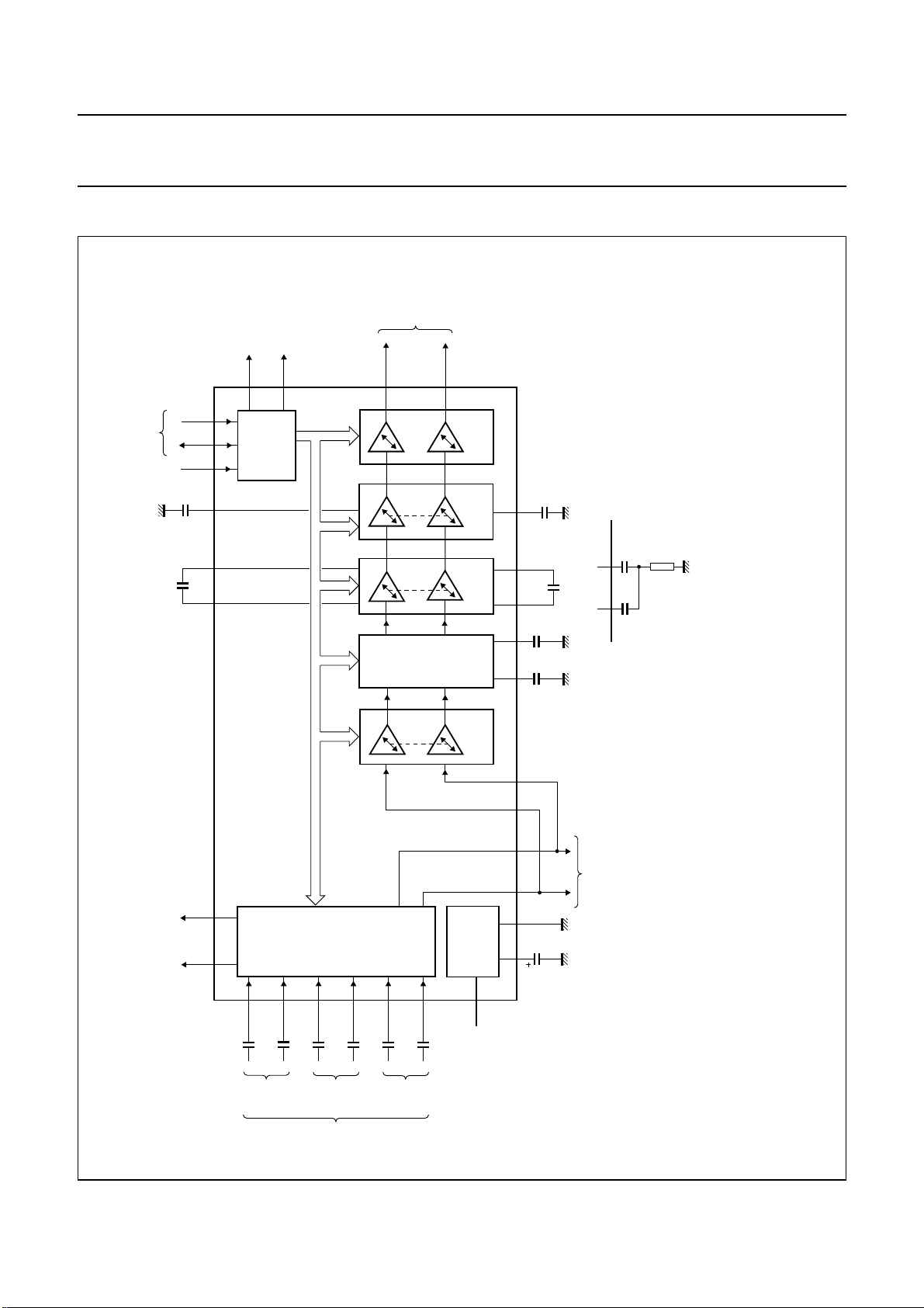
WIRING DIAGRAM……………………………………………………………………….9
BLOCK DIAGRAM………………………………………………………………………...10
IC BLOCK DIAGRAM……………………………………………………………………..11
SCHEMATIC DIAGRAM………………………………………………………………….15
ELECTRICAL PARTS LIST………………………………………………………………16
1
Page 3

CAUTION: THIS SERVICE MANUAL IS ONLY FOR PROFESSIONAL SERVICE PERSONNEL’S
REFERENCE. BEFORE SERVICING THIS CHASSIS, PLEASE READ THE
FOLLOWING NOTICE ITEMS.
1. SAFETY INSTRUCTION AND PRODUCT SAFETY NOTICE
Before servicing and aligning this equipment, please read the following “X-RAY RADIATION
PRECAUTION” ,“SAFETY PRECAUTION” and “PRODUCT SAFETY NOTICE”.
1.1 X-RAY RADIATION PRECAUTION
Excessive high voltage can produce potentially hazardous X-RAY RADIATION. To avoid such hazards,
1
the high voltage must not be above the specified limit. The normal value of the high voltage of this
receiver is: 26.5kV(25”) at 1.3mA beam current; 29kV(29” super flat) at 1.4mA beam current; 30kV(29”
pure flat) at 1.4mA beam current. The high voltage must not, under any circumstances, exceed
31kV(25”)/33kV(29”)/35kV(29” pure flat).
2
Each time a receiver requires servicing, the high voltage should be checked following the HIGH
VOLTAGE CHECK procedure in this manual. It is recommended the reading of the high voltage be
recorded as a part of service record. It is important to use an accurate and reliable high voltage meter.
The primary source of X-RAY RADIATION in this TV receiver is the picture tube. For continuous X-RAY
3
RADIATION protection, the replacement tube must be exactly the same type tube as specified in the parts
list.
Some parts in this receiver have special safety-related characteristics for X-RAY RADIATION protection.
4
For continuous safety, parts replacement should be undertaken only after referring to the PRODUCT
SAFETY NOTICE below.
1.2 SAFETY PRECAUTION
WARNING:
Service should not be attempted by anyone unfamiliar with the necessary precaution on this receiver. The
following are the necessary precautions to be observed before servicing this chassis.
1) Since the power supply circuit of this receiver is directly connected to the AC power line, an isolation
transformer should be used during any dynamic service to avoid possible shock hazard.
2) Always discharge the picture tube anode to the CRT conductive coating before handling the picture tube.
The picture tube is highly evacuated and if broken, glass fragments will be violently expelled. Use shatter
proof goggles and keep picture tube away from the unprotected body while handling.
3) When replacing a chassis in the cabinet, always be certain that all the protective devices are put back in
place, such as: non-metallic control knobs, insulating covers, shields, isolation resistor-capacitor network
etc.
4) When replacing parts or circuit boards, disconnect the power cord.
5) When replacing a high wattage resistor (oxiode metal film resistor) on the circuit board, keep the resistor
10mm (1/2in) away from circuit board.
1
Page 4
6) Connection wires must be kept away from components with high voltage or high temperature.
7) If any fuse in this TV receiver is blown, replace it with the FUSE specified in the chassis parts list.
8) Before returning the set to your customer, always perform an AC leakage current check on the exposed
metallic parts of the cabinet, such as antennas, terminals, screwheads, metal overlays, control shafts etc. to
be sure the set is safe to operate without danger of electrical shock. Plug the AC power cord into a 220V
AC outlet (do not use a line isolation transformer during this check). Use an AC voltmeter having 5000
ohms per volt or more sensitivity in the following manner:
Connect a 1500 ohm 10 watt resistor, paralleled by a 0.15µF, AC type capacitor, between a known good
earth ground (water pipe, conduit, etc.) and the exposed metallic parts, one at a time. Measure the AC
voltage across the combination of 1500 ohm resistor and 0.15µF capacitor. Reverse the AC plug at the AC
outlet and repeat AC voltage measurements for each exposed metallic part. Voltage measured must not
exceed 0.3 volts RMS. This corresponds to 0.2 milliamp. AC. Any value exceeding this limit constitutes a
potential shock hazard and must be corrected immediately.
AC VOLTMETER
µ
9) DC voltage breakdown test
Good earth ground
such as a water
pipe, conduit, etc.
C.
R.
Place this probe on
Each exposed
Metallic part.
Before packing, the following touchable parts should be conducted with withstand voltage test for 1s.
Apply the voltage and test, the voltage should be AC 3000V.
Part name : Position:
Antenna terminal Back cabinet
Outcabinet screws Back cabinet
AV terminals Back and side
1.3 PRODUCT SAFETY NOTICE
Many electrical and mechanical parts in the chassis have special safety-related characteristics. These
characteristics are often passed unnoticed by a visual inspection and the X-RAY RADIATION
protection afforded by them cannot necessarily be obtained by using replacement components rated for
higher wattage, etc. Replacement parts which have these special safety characteristics are identified in
this manual and its supplement electrical components having such features are shaded on the schematic
diagram and the parts list.
Before replacing any of these components, read the parts list in this manual carefully. The use of
substitute replacement parts which do not have the same characteristics as specified in the parts list may
create shock, fire, X-RAY RADIATION or other hazards.
2
Page 5
y
n
h
y
Col
C.E.C BELSON/DPTO.TECNICO/MOD:BSV-29251/Ed.01
2 Alignment procedure
The alignment procedure flow chart see below figure:
EEPROM copy
Chassis
B+ check
V-size V-linearit
rough adjust
H-size,
E/W pincushio
correction roug
adjust
RF AGC
Sound check
The whole unit
Focus rough adjust and
aging
VG2 adjust
White balance and
sub-brightness adjust
H-center V-center and
V-size realign
H-size and E/W
correction
OSD vertical position
Focus fine-adjust
Check
Fig.2
High voltage
check
Filament voltage
check
X-ray protection
check
Picture and
sound check
White balance
check
or purity
convergence
check
Luminance,
chroma time
dela
AV terminal
check
The TV set
button’s function
check
The remote
controller’s
function check
Installation and
packing check
Safety check
3. TEST EQUIPMENT
3.1 DC regulated power supply PAB18-1.8
3.2 Audio voltameter
3.3 Oscilloscope
3.4 High-voltage meter
3.5 Digital multimeter
3.6 AC break-down testing equipment
4 Alignment instruction
The way to enter into factory alignment menu by using remote control: when there is no OSD on the
screen, in turn press MIX, CANCEL, HOLD and REVEAL button and the period of two-press should be
less than 3 seconds. To exit, press TV button.
4.1 B+ confirm
Use DC voltameter of DC200V to check B+ voltage (C529 two terminals), 29” pure flat CRT should
be 140V or 138V (depending on different CRT), the error is
0.5 V.
4.2 AGC alignment
3
Page 6

4.2 AGC alignment
4.2.1 Receive D-8 signal 60 dB, use DC voltameter to measure C104 positive pole testing point voltage.
4.2.2 Adjust TOP item to make AGC voltage just start dropping from highest point (about 4V).
4.2.3 From antenna input inputs 100 dB signal, the picture should not appear non-synchronization and
distortion. Input 35 dB
40 dB weak signal, the colour should not appear and picture is in
synchronization and sound is normal.
4.3 Sound check
4.3.1 Receive 1kHz 100% modulation sound signal, XV03 connect with a simulated speaker load of 8 ohm,
audio voltmeter or oscilloscope measure the voltage of the load.
4.3.2 Turn the volume to maximum, the sound power consumption should be
the distortion should be
7% (allow maximum volume sine wave have clipping distortion)
7 W 2 (about 7.5 Vrms),
4.4 Focus potentiometer adjustment
4.4.1 The whole unit preheats 30 minutes.
4.4.2 Receive testing signal.
4.4.3 Press PP button to select DYNAMIC mode.
4.4.4 Adjust FBT’s FOCUS potentiometer to make picture clearest.
4.5 H-center adjustment
4.5.1 Receive 50 Hz testing signal.
4.5.2 Enter into 5HSH item, adjust the level to make picture symmetry in horizontal.
4.5.3 Receive 60Hz testing signal. To 6HSH adjust, the method is as same as the above two steps.
4.6 V-size, Vertical S-correction, V-center, H-size, E/W correction adjustment (50 Hz/60 Hz
independently)
4.6.1 Receive testing signal, enter into factory menu VSL item, adjust the value to make picture’s lower half
part just disappear.
4.6.2 Enter into factory menu corresponding item, adjust the value to make V-center and CRT’s geometrical
center be in accordance, vertical S-linearity be proper and vertical reproduction rate be
90%.
4.6.3 Enter into factory menu corresponding items, adjust horizontal geometrical distortion until be in proper.
EWW Adjust H-size
EWP Adjust east/west pincushion correction size
EWT Adjust east/west trapezoid size
UCT Adjust east/west left upper corner and right upper corner distortion
LCR Adjust east/west left lower corner and right lower corner distortion.
BOW Adjust east/west arch.
PAR Adjust parallelogram.
The adjustment results meet scan linearity geometrical distortion and over-scan (reproduction rate)
requirements.
4.7 Screen-grid voltage VG2 adjustment
Enter into factory menu, set VG2B to 29, press digit button “0”, enter into alignment status, turn FBT
accelerated pole potentiometer to end anticlockwise, then clockwise turn the potentiometer until the
indication “OUTSIDE LOW” just jump to “INSIDE HIGH”.
4.8 White balance adjustment (auto dark balance)
4.8.1 Dark balance just need fine tune, under 4.5 nit, colour temperature 12000K+8MPCD (X=0.270,
Y=0.283)
4.8.2 Bright balance also has already automatically adjusted at some white coordinate. Only need to fine tune
around 31 value, under 60 nits, colour temperature 12000K+8MPCD (X=0.270, Y=0.283)
4
Page 7

4.9 Luminance/chroma time delay adjustment (YD_ _)
Respectively input PAL,SECAM,NTSC RF signal or PAL AV signal and adjust YD_ _ to make
luminance tallied with chroma.
For those model with SVM function, on the condition that SVM is set to ON, input split field or
crosshatch signal, respectively adjust YD_ _ until SVM’s edge from black to white is in symmetry with
that from white to black, give attention to the data that make luminance tallied with chroma.
4.10 High voltage and filament voltage check
4.10.1 Connect high voltage meter between CRT high voltage cap and GND, use effective and precise
voltameter to measure filament voltage.
4.10.2 Receive D35 signal, set picture mode to “DYNAMIC”. Measure the high voltage and filament voltage
and the reading should be: for 29” super flat CRT, the high voltage is 29 kV
flat CRT, the high voltage is 30 kV
0.5 kV, filament voltage 6.3 0.3 Vrms.
0.5 kV, for 29” pure
4.11 X-ray protection check
4.11.1 Receive normal picture.
4.11.2 Press S301 switch, horizontal scan should stop vibration and turn off.
4.11.3 Turn off the power switch and wait about 30 seconds, turn on the set again, it should restore to
normal.
4.12 Beam current check
Receive D35 signal, set picture mode to “DYNAMIC”, measure R313 two terminals, for 29” super flat
it should be
1.6 V, for 29” pure flat it should be 1.7V.
4.13 AV function check
According to Instruction manual, connect the AV equipment to the AV terminals which need to be
check, the following is required:
VIDEO IN: 1 Vp-p 75
, AUDIO IN: -8 dBm 3 dBm 47 k .
4.14 Out-factory status setting
Contrast: 45 Comb filter: ON
Brightness: 28 Blue back: ON
Colour: 40 Black stretch: ON
Sharpness: 35 SVM: ON
Treble: 31 AVL: OFF
Bass: 31 Surround: OFF
Balance: 0
The following appendix is factory menu and data.
5
Page 8
C.E.C BELSON/DPTO.TECNICO/MOD:BSV-29251/Ed.01
Appendix 1 factory menu and data
Page/
Button
1
2
1
Item Meaning Reference value Remark
5PAR Horizontal parabola 0-63
5BOW Horizontal bow 0-63
5HSH Horizontal shift 0-63
5EWW EW width 0-63
5EWP EW parabola 0-63
5UCR EW upper corner parabola 0-63
5LCR EW lower corner parabola 0-63
5EWT EW trapezium 0-63
5VSL Vertical slope 0-63
5VAM Vertical amplitude 0-63
5SCL S-Correction 0-63
5VSH Vertical Shift 0-63
5VOF Text Position Vertical offset
6PAR Horizontal parabola 0-63
6BOW Horizontal bow 0-63
6HSH Horizontal shift 0-63
6EWW EW width 0-63
For 50Hz
41
6EWP EW parabola 0-63
6UCR EW upper corner parabola 0-63
6LCR EW lower corner parabola 0-63
6EWT EW trapezium 0-63
6VSL Vertical slope 0-63
2
RED WPR White Point R 0-63
GREEN WPG White Point G 0-63
6VAM Vertical amplitude 0-63
6SCL S-Correction 0-63
6VSH Vertical Shift 0-63
6VOF Text Position Vertical offset
VX Vertical Zoom
RED Black level offset R 32
GRN Black level offset G 32
28
25
3
BLUE WPB White Point B 0-63
YDFP Y-Delay for PAL
YDFN Y-Delay for NTSC
YDFS Y-Delay for SECAM
YDAV Y-Delay for AV
4 TOP AGC Take-Over Point 0-63
0-15
For 60Hz
Adjust around 31
Brightness, colour in
accordance. For model
with SVM function,
SVM edge should be
in symmetrical.
6
Page 9
C.E.C BELSON/DPTO.TECNICO/MOD:BSV-29251/Ed.01
VOL Volume
9874 Gain control for TDA9874
IFFS Vision IF
HDOL Cathode drive level
AGC IF AGC speed
AG2B VG2 Brightness 33 Before adjust AG2, fix it
OP1 Option byte 1 218 (11011010)
OP2 Option byte 2 33 (00100001)
5
6 INT Initial E2PROM According to actual need initial EEPROM
7 LOGO Logo According to actual need set the logo.
8 STS Status
9 AGIN Aging(escape by local Menu) Press Menu button on the set to exit.
0 VG2 Adjust VG2
Note1: the letter in bold and italic is fixed setting.
Note2: use blank EEPROM, after turning on the set for the first time, please first initial EEPROM (at INT item
press VOL+ button), and reset other factory menu item.
OP3 Option byte 3 123 (01111011)
OP4 Option byte 4 251 (11111011)
OP5 Option byte 5 63 (00111111)
45
20
2
8
1
‘In High’/’Out Low’
or line disappear
2-38.9M,3-38M
7
Page 10

C.E.C BELSON/DPTO.TECNICO/MOD:BSV-29251/Ed.01
Addendix2 Option byte 1-5 meaning
Bit Option 1 Option 2 Option 3 Option 4 Option 5
7
6
5
4
3
2
1
0
Note1: the letter in bold and capital is fixed setting.
Note2: for model without NICAM, please set AVL=0.
Note3: for sound filter in absorbing type in main board (for example K3959D), please set AUTO SOUND=0.
OSD1 FSL2
1-enable 0-disable 0- disable 1- disable
Reserved
1
DVD Sound BG PSNS Italian
0- RGB
1-enable 1-enable 1-TDA9363 1-enable
1-enable 1-enable 1-enable 1-enable
0-disable
1-enable 1- disable
0-normal mode 1-enable 1-enable
1)OSO Switch Off in vertical Over Scan
2)FSL Forced Slicing Level
3)Function SVM is disable when in RGB,DVD,TEXT or SECAM mode
4)PSNS More PAL color sensitivity for Asian market areas
5)FMWS Active when M system
1-DVD
SVHS Sound DK HCO French
AV2 Secam-SVM LOGO German
Super woofer
Comb filter Auto sound EEPROM Spanish
VG2 mode AVL AFC Store FMWS English
Function
01-SVM
10-BBE
11-SRS
00-none
000-Pan Euro
001-Ukrainian
010-Russian
011-Farsi
100-Arabic
3
Teletext
Sound M DFL
Sound I OSD syn.
1-enable 1-stable
1-enable
Off-RBL AKB Arabic
0-enable 0-on 1-enable
1-8k 250prg
4
1-more
1-Memory Stb
0-Power on Stb
1- large
Switch on
5
Reserved
Reserved
1-enable
1-enable
1-enable
8
Page 11

C.E.C BELSON/DPTO.TECNICO/MOD:BSV-29251/Ed.01
Page 12

C.E.C BELSON/DPTO.TECNICO/MOD:BSV-29251/Ed.01
RF
TUNER101
TDQ-3B9H
BAND-UV
AGC
BAND-HL
SW
P2
VT
IF
SW
P2
SAW
SIF
N201
ST24C08
EEPROM
Z205 K2958M
ZZ01
K9260M
IF1
IF2
BAND-HL
BAND-UV
IIC
AGC
VT
NZ01
LA7510
SIF'
IIC
NZ02
TDA9874AH
MONO
FM MONO
Audio
Out
L
R
L R
NA03 TC4052BP
N203 TDA9363N2
Audio
Scart
Out
L R L RL RL R
In 2
Scart
In
NV01 TDA9859
L
R
Audio
In 1
AV0
P2
P1-MUTE
IIC
L
R
RGB 3
Ib
V-drive
Guard
H-drive
FB
+8V
EW
L R
N511
TDA8944J
RGB 3
TDA6107J
TDA8359J
+16V +45V
T302 FBT
N801
N350
H.D
EHT
E/W
V
H
EHT
De-Gauss
VIDEO OUT
SCART OUT
AV-3
AV-2
VIDEO IN 1
AV-1
S-VIDEO
TV
SCART IN
VIDEO IN 2
Y IN
C IN
NA02
TC4052BP
P2
NA01
TC4052BP
ZA01
ZA02
ZA03
ZA04
SIF TRAP
AV0
AV1
V/Y
C
P/N
S.C.
Sys2Sys1
FSC
BN01 TDA9181
+140V
Standby
3.3V
SMPS
5V
N502 TDA16846
8V
V501 SPP11N60S5
CY
G
Y
BUR
V
To AV-3 scart in
(when YUV used)
BL
AV/TV
(From Scart)
15V
+140V
Page 13

C.E.C BELSON/DPTO.TECNICO/MOD:BSV-29251/Ed.01
Philips Semiconductors Tentative Device Specification
Integrated multistandard comb filter TDA9181
BLOCK DIAGRAM
out
Y/CVBS
out
C
OUTSEL
DD
V
CC
V
LPF
adaptive
comb
LPF
filter
sc
4 x f
clock
generator
AGND DGND
SYS2SYS1
FSCSEL
delay
2H/4H
LPF
clamp
2
Y/CVBS
INPSEL
clamp
1
Y/CVBS
1999 Jun 14 3
FSC
Fig.1 Block diagram
filter
tuning
(LPFs)
detector
sandcastle
in
C
SC
Page 14
C.E.C BELSON/DPTO.TECNICO/MOD:BSV-29251/Ed.01
Philips Semiconductors Preliminary specification
Universal hi-fi audio processor for TV TDA9859
BLOCK DIAGRAM
outputs
channel
loudspeaker
C-bus
2
I
MAD SDA SCL
33 nF
5.6 nF
(1)
C
C
C
TL
BL2
BL1
P1
P2
2
31
C-BUS
2
I
INTERFACE
19 25 17 16
22 21
L
L
LOUT
18
STEREO
SPATIAL
MUTE
PSEUDO
STEREO
R
R
LOUT
15
STEREO
VOLUME
BALANCE
TREBLE
CONTROL
BASS
CONTROL
MONO
FORCED
14
11 12
29 27
MHA778
BR2
C
(1)
BR1
C
5.6 nF
TR
(1)
C
33 nF
PS2
extended bass control
C
PS1
C
11 (22) 12 (21)
0.15 µF
13 kΩ
68 nF
width
R
SCOUT
L
output
SCART
LR
SCOUT
VOLUME
CONTROL
R
23 10
24 9
48
VOLTAGE
LIN
L
LIN
R
MOUT
L
MOUT
LR
GND
100
SMO
C
LINE output or optional
µF
connection
surround sound decoder
should be replaced by the extended bass control network.
BR/L2
Fig.1 Block diagram and application circuit.
and C
BR/L1
(1) For extended bass control, the capacitor between C
TDA9859
26 7
28
L
AIN
L
30
R
AIN
470 nF
AUX
SOURCE
MULTIPLE
AND MODE
1
L
SCIN
470 nF
L
R
SELECTOR
470 nF
SCART
audio
32
R
SCIN
R
inputs
SWITCH)
(CROSSBAR
3
L
MIN
470 nF
470 nF
L
5
R
MIN
MAIN
R
470 nF
REFERENCE
6
P
V
+8 V
1997 Sep 01 3
Page 15

C.E.C BELSON/DPTO.TECNICO/MOD:BSV-29251/Ed.01
Philips Semiconductors Product specification
Digital TV sound demodulator/decoder TDA9874A
4 BLOCK DIAGRAM
handbook, full pagewidth
P1
P2
ADDR1
ADDR2
SCL
SDA
XTALI
XTALO
SYSCLK
SDO
WS
SCK
41 (37)
4 (42)
18 (13)
23 (19)
33 (29)
34 (30)
20 (15)
19 (14)
38 (34)
35 (31)
36 (32)
37 (33)
2
C-BUS
I
INTERFACE
IDENTIFICATION
CLOCK
PEAK
DETECTION
I2S-BUS
INTERFACE
SIF2
27 (23)
INPUT SWITCH
FM/AM
DEMODULATION
DEMATRIX
2-CHANNEL
ANALOG/
SATELLITE
DECODER
DIGITAL
SELECTOR
AGC, ADC
DEMODULATION
SIF1
29 (25)
NICAM
NICAM
DECODER
LEVEL
ADJUST
POST FILTER
3 DACs
SUPPLY
SIF
DIGITAL
SUPPLY
SUPPLY
DACs
OPAMPS
REFERENCE
(21) 25
(20) 24
(28) 32
(27) 31
(24) 28
(18) 22
(10) 15
(12) 17
(7) 13
(6) 12
(5) 11
(35) 39
(36) 40
(26) 30
(3) 9
(4) 10
(44) 6
(41) 3
(8)
V
DEC
V
SSA2
V
DDA3
V
SSA3
V
ref1
I
ref
NICAM
PCLK
n.c.
V
SSD2
V
DDD1
V
SSD1
V
DDD3
V
SSD3
CRESET
V
DDA1
V
SSA1
V
SSA4
V
ref2
TDA9874APS
(TDA9874AH)
TP1
TP2
TP3
26 (22)
21 (17)
16 (11)
14 (9)
(16)
TEST
TEST1
TEST2
The pin numbers given in parenthesis refer to the TDA9874AH.
Fig.1 Block diagram.
2000 Aug 04 6
CROSSBAR
MONO
CHANNEL
OUTPUT
BUFFERS
5 (43)
OUTM
ANALOG
SWITCH
2-CHANNEL
OUTL OUTR
OUTPUT
BUFFERS
7 (1) 8 (2)
(39) 1
(40) 2
(38) 42
MHB584
EXTIR
EXTIL
MONOIN
Page 16

C.E.C BELSON/DPTO.TECNICO/MOD:BSV-29251/Ed.01
Philips Semiconductors Tentative Device Specification
TV signal processor-Teletext decoder with
embedded µ-Controller
BLOCK DIAGRAM
61
+3.3 V
SDASCL
54 56
12
9
I/O PORTS (4x)
5-8
ADC IN (4x)
VST OUT
34
2
10/11
LED OUT (2x)
1/10 PAGE
MEMORY
1+62-64
C-BUS
2
I
TRANSCEIVER
VST PWM-DAC
I/O PORTS
DISPLAY
TELETEXT/OSD
V
H
TELETEXT
ACQUISITION
CVBS
ROGOB0
515253
BL
B
RG
CONTR/BRIGHTN
OSD/TEXT INSERT
COR
SYNC
TDA935X/6X/8X PS/N1 series
BLKIN
BCLIN
49
50
45
484746
CCC
GB
R
WHITE-P. ADJ.
RGB/YUV INSERT
SATURATION
RGB/YUV MATRIX
YUV/RGB MATRIX
Y
U
V
(20)
(EW GEOMETRY)
G/Y B/U BL
R/V
EWD
36
EHTO
TRAP
SOUND
VPE
RESET
AUDOUT
AUDEXT
SNDIF
TUNERAGC
60 55 59 58 57
44
35
29 28
(20)
31
(32)
27 37 38
(32)
80C51 CPU
ENHANCED
(AVL)
DEEMPHASIS
AUDIO SWITCH
VOLUME CONTROL
AGC/AFC
VISION IF
23
VIDEO AMP.
PLL DEMOD.
ALIGNMENT-FREE
24
IFIN
ROM/RAM
PLL
AGC CIRCUIT
NARROW BAND
DEMODULATOR
VIDEO IDENT.
VIDEO SWITCH
VIDEO FILTERS
42
40
43
CHROMA
CVBS/Y
PEAKING
LUMA DELAY
BASE-BAND
REF
REF
PAL/SECAM/NTSC
13
BLACK STRETCH
DELAY LINE
DECODER
30
41
(32)
18
V-DRIVE +
GEOMETRY
V
LOOP
nd
H-SHIFT
H-DRIVE
2
H
H-OSC. + PLL
H/V SYNC SEP.
19
39
14
+8V
21
222625
33
16
34
HOUT V-DRIVE
Fig. 1 Block diagram TDA935X/6X8X with mono intercarrier sound demodulator
17
15
2000 Jul 25 6
Page 17

C.E.C BELSON/DPTO.TECNICO/MOD:BSV-29251/Ed.01
Page 18

C.E.C BELSON/DPTO.TECNICO/MOD:BSV-29251/Ed.01
Page 19

C.E.C BELSON/DPTO.TECNICO/MOD:BSV-29251/Ed.01
Page 20
C.E.C BELSON/DPTO.TECNICO/MOD:BSV-29251/Ed.01
WARNING: BEFORE SERVICING THIS CHASSIS, READ THE “X-RAY RADIATION
PERCAUTION”, “SAFETY PRECAUTION” AND “PRODUCT SAFETY NOTICE” ON
PAGE 1&2 OF THIS MANUAL.
CAUTION: 1. The shaded areas makes in the schematic diagram and the parts list designate components
which have special characteristics important for safety and should be replaced only with
type identical to those in the original circuit or specified in the parts list. Before replacing
any of these components, read carefully the PRODUCT SAFETY NOTICE on page 2.
2. Do not degrade the safety of the receiver through improper servicing.
ELECTRICAL PARTS LIST
MAIN BOARD
SYMBOL PART NO. DESCRIPTION
G201 329-61203-00 JA117 12M
D501 340-80015-00 RS405G
D510 340-80012-00 FMLG12S
D206 340-50200-003 HZ2B1
D508 340-50410-003 HZ4C1
D320 340-50520-003 HZ5C3
D201 340-50550-003 HZ6A3
D202 340-50550-003 HZ6A3
D350 340-51260-003 HZ12B1
D313 340-51560-003 HZ16-1
D307 340-52990-003 HZ30-2
V501 343-00600-50 SPP11N60S5
V301 343-15690-00 2SC1569
V302 343-25530-00 2SD2553
V303 343-52480-30 2SC5248E
VV01 343-18150-704 2SC1815-GR
V202 343-10150-104 2SA1015Y Pr2.5
V203 343-10150-104 2SA1015Y Pr2.5
V304 343-10150-104 2SA1015Y Pr2.5
VA01 343-10150-104 2SA1015Y Pr2.5
VA08 343-10150-104 2SA1015Y Pr2.5
16
782-H2917-0100
CRYSTAL
RECTIFIER
REGULATED DIODE
TRANSISTOR
MAIN PCB
Page 21

C.E.C BELSON/DPTO.TECNICO/MOD:BSV-29251/Ed.01
SYMBOL PART NO. DESCRIPTION
V502 343-18150-104 2SC1815-Y
VA02 343-18150-104 2SC1815-Y
VA03 343-18150-104 2SC1815-Y
VB01 343-18150-104 2SC1815-Y
VB02 343-18150-104 2SC1815-Y
VV02 343-18150-104 2SC1815-Y
VV03 343-18150-104 2SC1815-Y
V503 343-18150-104 2SC1815-Y
V201 343-18150-704 2SC1815-GR
V305 343-18150-704 2SC1815-GR
V306 343-18150-704 2SC1815-GR
V101 343-23690-004 PH2369
V106 343-27170-004 2SC2717
Z201 458-05022-00 K3959D
R355 467-2D215-G03 1/4W-1.5K-G
R356 467-2D215-G03 1/4W-1.5K-G
R518 467-2E110-H0 1/2W-100Ω-JL
R310 467-2FA22-H0 1W-2.2Ω-JL
R361 467-2F001-H0 1W-1Ω-JL
R351 467-2F010-H0 1W-10Ω-JL
R318 467-2F133-H0 1W-330Ω-JL
R328 467-2F133-H0 1W-330Ω-JL
R303 467-2F227-H0 1W-2.7KΩ-JL
R329 467-2F247-H0 1W-4.7K-JL
R326 467-2F351-H0 1W-51kΩ-JL
R516 467-2G022-H0 2W-22Ω-JL
R360 467-2G127-H0 2W-270Ω-JL
R304 467-2G318-H0 2W-18kΩ-JL
SAW FILTER
METAL RESISTOR
INDUCTANCE WITH COLOUR CODES
LB02 471-2010K-003 SPT0305-100K-5
L101 471-2010K-003 SPT0305-100K-5
L203 471-2010K-003 SPT0305-100K-5
L204 471-2010K-003 SPT0305-100K-5
L206 471-2010K-003 SPT0305-100K-5
L207 471-2010K-003 SPT0305-100K-5
LA14 471-2010K-003 SPT0305-100K-5
LA15 471-2010K-003 SPT0305-100K-5
LB01 471-2010K-003 SPT0305-100K-5
L504 471-2068K-103 LGA0410-68uH-K
LA02 471-1010K-00 EL0606SKI-100K
17
Page 22

C.E.C BELSON/DPTO.TECNICO/MOD:BSV-29251/Ed.01
SYMBOL PART NO. DESCRIPTION
L201 471-1010K-00 EL0606SKI-100K
L202 471-1010K-00 EL0606SKI-100K
LA07 471-1010K-00 EL0606SKI-100K
LA01 471-1010K-00 EL0606SKI-100K
LA06 471-1010K-00 EL0606SKI-100K
LA10 471-2A68K-A0 SP0203-6.8uH-K
LA12 471-2A68K-A0 SP0203-6.8uH-K
L102 471-2001K-A0 SP0203-1uH-K
L208 471-2010K-00 SPT0305-100K-5
RV02 467-4FA56-H0 1W-5.6Ω-JL
R317 467-4FB33-H0 1W-0.33Ω-JL
R321 467-4FA27-H0 1W-2.7Ω-JL
R314 467-4FB33-H0 1W-0.33Ω-JL
R315 467-4FB33-H0 1W-0.33Ω-JL
R528 467-4FB33-H0 1W-0.33Ω-JL
R529 467-4FB33-H0 1W-0.33Ω-JL
R530 467-4FB68-H0 1W-0.68Ω-JL
R319 467-4F001-H0 1W-1Ω-JL
R354 467-4F001-H0 1W-1Ω-JL
R510 467-4GA22-H0 2W-2.2Ω-JL
R507 467-4GB27-H0 2W-0.27Ω-JL
R317 467-4FA15-H0 1W-1.5Ω-JL
RV02 467-4FA56-H0 1W-5.6Ω-JL
R317 467-4FB33-H0 1W-0.33Ω-JL
MELTABLE RESISTOR
IC
N510 *352-11170-70 GS1117CT-3.3
N502 352-02540-40 TNY254P
N506 352-04310-00 LM431A
N301 352-05740-00 uPC574
N503 352-06210-60 TLP621-GB
N504 352-06210-60 TLP621-GB
N505 352-06210-60 TLP621-GB
N501 352-16846-00 TDA16846
N202 352-24080-50 M24C08BN6
NA01 352-40520-60 TC4052BP
N507 352-78050-00 KA7805
N508 352-78080-00 AN7808
N350 352-83590-90 TDA8359J/N2
NV02 352-89440-70 TDA8944J
NB01 352-91810-00 *TDA9181P
N201 352-93630-00 *TDA9363PS/N2/5I
18
Page 23

C.E.C BELSON/DPTO.TECNICO/MOD:BSV-29251/Ed.01
SYMBOL PART NO. DESCRIPTION
NV01 352-98590-00 TDA9859
C503 459-B147M-20 ECK-DNS471MBX !
C504 459-B147M-20 ECK-DNS471MBX !
C548 459-B222M-20 ECK-DNS222MEX !
C505 459-B247R-00 DE0807F472ZAC250V !
C506 459-B247R-00 DE0807F472ZAC250V !
C507 459-B247R-00 DE0807F472ZAC250V !
C508 459-B247R-00 DE0807F472ZAC250V !
L302 477-40020-00 LE1919
L506 477-40028-00 L912
L505 477-40057-00 LG101
L304 477-40107-00 160uH
477-40205-00 * LEY-433-1T
T302 472-27130-00 BSC29-3991N !
CERAMIC CAPACITOR
FIXED INDUCTANCE
FBT
POWER TRANSFORMER
T502 470-00191-00 SRW16ES-X03V112 !
SWITCH TRANSFORMER
T501 470-00269-00 BCK200-1D !
CERAMIC TRAP FILTER
ZA02 475-25551-00 XT5.5MB
ZA01 475-25601-00 XT6.0MB
ZA04 475-25651-00 XT6.5MB
POWER FILTER
L502 477-20047-00 LCL-205
H-LINEARITY INDUCTANCE
L305 477-00057-00 HL1835H-X10
H-DRIVE TRANSFORMER
T301 472-10027-00 HTB-835
CEMENT RESISTOR
R301 467-50251-H8 RJG27-3C-5W-5.1K-J
R514 467-50322-H8 RJG27-3C-5W-22K-J
R502 467-51127-H4 RX27-3H-7W-270Ω-J
VITREOUS-ENAMEL RESISTOR
R504 467-7F447-H0D RI40-1W-470K-JL
WIRE-ROUND RESISTOR
R352 467-6FA15-H0 RX21-1-1.5Ω-J
R353 467-6FA15-H0 RX21-1-1.5Ω-J
CARBON RESISTOR
R505 467-8E539-K0 1/2W-3.9MΩ-KL !
19
Page 24

C.E.C BELSON/DPTO.TECNICO/MOD:BSV-29251/Ed.01
SYMBOL PART NO. DESCRIPTION
R534 467-8E582-H0A 1/2W-8.2MΩ-J !
RT501 469-10007-00 PTH451C262BG200N270
RT502 469-40004-00 5D2-14LC
DEGAUSSING COIL 477-12801-00 BD-205-3 !
POWER SWITCH 360-30028-00 KDC-A04-S !
POWER CORD 493-75710-07 VDE !
CRT 335-2932H-00 A68QCP891X001 !
TUNER101 590-30533-00 TDQ-3B9H/124XS !
SYMBOL PART NO. DESCRIPTION
782-H2917-3100 NICAM PCB
THERMISTOR
OTHER
NICAM BOARD
CRYSTAL
GZ01 329-62404-00 HC-49/US 24.576MHZ
TRANSISTOR
VZ04 343-18150-60 2SC1815-0
VZ05 343-18150-60 2SC1815-0
VZ01 343-27170-00 2SC2717
IC
NZ01 352-75100-00 LA7510
NZ02 *352-98740-10 TDA9874AH
SAW FILTER
ZZ01 458-05023-00 K9260M
INDUCTANCE WITH COLOUR CODES
LZ02 471-1110H-00 EL0606SKI-101J
LZ03 471-1110H-00 EL0606SKI-101J
LZ01 471-2001K-00 SPT0305-1R0K-5
BUTTON BOARD
SYMBOL PART NO. DESCRIPTION
782-H2930-0500 BUTTON PCB
TRANSISTOR
V902 343-18150-10 2SC1815-Y
V903 343-18150-10 2SC1815-Y
LIGHT-EMITTING DIODE
VD901 340-10055-90 HFT505M
METAL RESISTOR
R915 467-2D218-G0 1/4W-1.8K-G
R916 467-2D236-G0 1/4W-3.6K-G
20
Page 25

C.E.C BELSON/DPTO.TECNICO/MOD:BSV-29251/Ed.01
SYMBOL PART NO. DESCRIPTION
RC901 352-03810-80 AT138B-T12 (M)
SYMBOL PART NO. DESCRIPTION
782-H2930-2900 SIDE AV PCB
RAA9 467-2E115-H0 1/2W-150Ω-JL
RAA10 467-2E115-H0 1/2W-150Ω-JL
RAA11 467-2E118-H0 1/2W-180Ω-JL
RAA12 467-2E118-H0 1/2W-180Ω-JL
INDUCTANCE WITH COLOUR CODES
LAA1 471-2010K-A0 SP0203-10uH-K
LAA2 471-2010K-A0 SP0203-10uH-K
LAA3 471-2010K-A0 SP0203-10uH-K
IC
SIDE AV BOARD
METAL RESISTOR
CRT BOARD
SYMBOL PART NO. DESCRIPTION
782-R2990-020A CRT PCB
DIODE
VD801 340-00010-00 S5295G
VD802 340-00010-00 S5295G
VD803 340-00010-00 S5295G
IC
N801 352-61070-70 TDA6107JF (M)
CRT SOCKET
X803 364-58220-00 GZS10-301D !
METAL RESISTOR
R809 467-2G110-H0 2W-100Ω-JL
MELTABLE RESISTOR
R810 467-4GA22-H0 2W-2.2Ω-JL
CARBON RESISTOR
R804 467-8E227-H0A 1/2W-2.7KΩ-J !
R805 467-8E227-H0A 1/2W-2.7KΩ-J !
R806 467-8E227-H0A 1/2W-2.7KΩ-J !
METAL RESISTOR
R801 467-2E110-H0 1/2W-100Ω-JL
R802 467-2E110-H0 1/2W-100Ω-JL
R803 467-2E110-H0 1/2W-100Ω-JL
21
Page 26

C.E.C BELSON/DPTO.TECNICO/MOD:BSV-29251/Ed.01
VM BOARD
SYMBOL PART NO. DESCRIPTION
782-29FA0-6400 VM PCB
DIODE
VD611 340-00001-00 1N4148
VD606 340-00001-00 1N4148
VD604 340-00001-00 1N4148
VD603 340-00001-00 1N4148
VD607 340-00001-00 1N4148
VD608 340-00001-00 1N4148
VD610 340-00079-00 FR103
VD609 340-00079-00 FR103
TRANSISTOR
V603 343-07520-10 2SC752GTM-Y
V607 343-07520-10 2SC752GTM-Y
V610 343-10150-11 2SA1015Y
V602 343-10150-11 2SA1015Y
V615 343-12060-00 RN1206
V614 343-12060-00 RN1206
V613 343-12060-00 RN1206
V604 343-18150-11 2SC1815-Y
V605 343-18150-11 2SC1815-Y
V606 343-18150-11 2SC1815-Y
V609 343-18150-11 2SC1815-Y
V619 343-18150-11 2SC1815-Y
V620 343-18150-11 2SC1815-Y
V601 343-18150-11 2SC1815-Y
V611 343-19640-30 2SA1964E
V612 343-52480-30 2SC5248E
METAL RESISTOR
R640 467-2EA27-G0 1/2W-2.7Ω-GL
R639 467-2EA27-G0 1/2W-2.7Ω-GL
R630 467-2E010-H0 1/2W-10Ω-JL
R638 467-2E033-H0 1/2W-33Ω-JL
R642 467-2E033-H0 1/2W-33Ω-JL
R644 467-2E068-H0 1/2W-68Ω-JL
R628 467-2E133-H0 1/2W-330Ω-JL
R619 467-2E147-H0 1/2W-470Ω-JL
R643 467-2F115-H0 1W-150Ω-JL
INDUCTANCE WITH COLOUR CODES
L601 471-2047K-A0 SP0203-47uH-K
22
Page 27

C.E.C BELSON/DPTO.TECNICO/MOD:BSV-29251/Ed.01
SYMBOL PART NO. DESCRIPTION
Z602 475-25361-00 TPS3.58MJ
Z601 475-25441-00 TPS4.43M
DL601 591-10018-00 YBL 48E08
POWER FILTER BOARD
SYMBOL PART NO. DESCRIPTION
782-66830-511A POWER FILTER PCB
462-2B410-M0V 250VAC-0.1uF-M !
467-8E522-H0A 1/2W-2.2M-J !
477-20031-00 LCL-21 !
CERAMIC TRAP FILTER
BRIGHTNESS DELAY LINE
THIN-FILM CAPACITOR
CARBON RESISTOR
POWER FILTER
FUSE
569-14141-80 50T 4AL 250V !
DYNAMIC FOCUS BOARD
PART NO. DESCRIPTION
782-29FA0-711B DYNAMIC FOCUS PCB
CARBON RESISTOR
467-8E227-H1A 1/2W-2.7KΩ-J !
DYNAMIC FOCUS TRANSFORNIER
472-60001-00 BCT222
ADJUSTABLE INDUCTANCE
477-30011-00 TLN2110
23
 Loading...