

Page 1

Operating instructions for
KL4011 and KL4012
Single- and Two-Channel Analog Output Terminals
Signal range: 0 to 20 mA
and
KL4021 and KL4022
Single- and Two-Channel Analog Output Terminals
Signal range: 4 to 20 mA
Version: 3.1
Date: 2006-10-20
Page 2

Table of contents
KL401x and KL402x
Table of contents
1. Foreword 1
Notes on the documentation 1
Safety Instructions 2
2. Technical data 3
3. Connection 4
KL4011 and KL4021 4
KL4012 and KL4022 4
4. Functional description 5
5. Terminal configuration 6
6. Register Description 7
General Description of Registers 7
Terminal-specific register description 10
Control and Status byte 12
Register communication 12
7. Appendix 14
Mapping 14
Register Table 16
Support and Service 17
Page 3

Foreword
KL401x and KL402x 1
Foreword
Notes on the documentation
This description is only intended for the use of trained specialists in control and automation engineering
who are familiar with the applicable national standards. It is essential that the following notes and
explanations are followed when installing and commissioning these components.
Liability Conditions
The responsible staff must ensure that the application or use of the products described satisfy all the
requirements for safety, including all the relevant laws, regulations, guidelines and standards.
The documentation has been prepared with care. The products described are, however, constantly under
development. For that reason the documentation is not in every case checked for consistency with
performance data, standards or other characteristics. None of the statements of this manual represents a
guarantee (Garantie) in the meaning of § 443 BGB of the German Civil Code or a statement about the
contractually expected fitness for a particular purpose in the meaning of § 434 par. 1 sentence 1 BGB. In
the event that it contains technical or editorial errors, we retain the right to make alterations at any time
and without warning. No claims for the modification of products that have already been supplied may be
made on the basis of the data, diagrams and descriptions in this documentation.
Delivery conditions
In addition, the general delivery conditions of the company Beckhoff Automation GmbH apply.
Copyright
©
This documentation is copyrighted. Any reproduction or third party use of this publication, whether in
whole or in part, without the written permission of Beckhoff Automation GmbH, is forbidden.
Page 4
Foreword
2 KL401x and KL402x
Safety Instructions
State at Delivery
All the components are supplied in particular hardware and software configurations appropriate for the
application. Modifications to hardware or software configurations other than those described in the
documentation are not permitted, and nullify the liability of Beckhoff Automation GmbH.
Description of safety symbols
The following safety symbols are used in this documentation. They are intended to alert the reader to the
associated safety instructions..
Danger
This symbol is intended to highlight risks for the life or health of personnel.
Attention
This symbol is intended to highlight risks for equipment, materials or the
environment.
i
Note
This symbol indicates information that contributes to better understanding.
Page 5
Technical data
KL401x and KL402x 3
Technical data
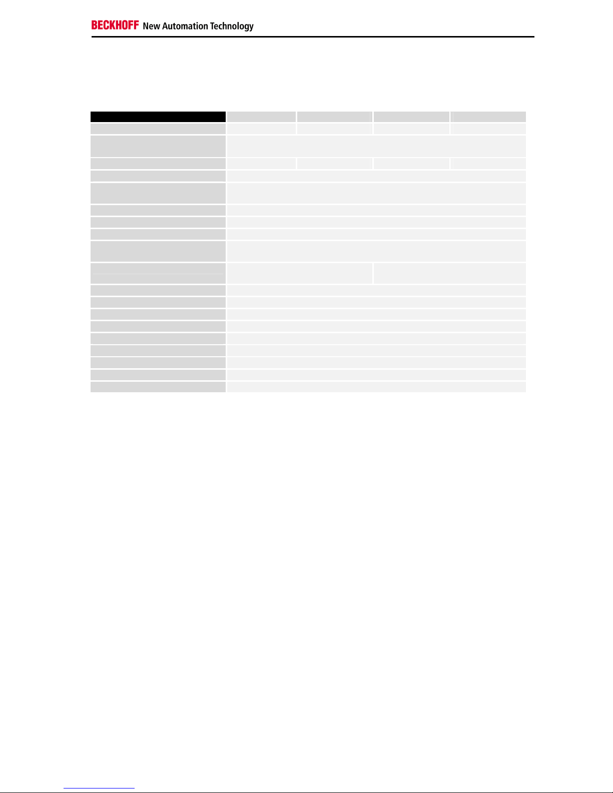
Technical data KL4011 KL4021 KL4012 KL4022
Number of outputs
1 1 2 2
Power supply
24 VDC via the power contacts
(alternatively 15 VDC with power supply unit terminal KL9515)
Signal voltage
0 ... 20 mA 4 ... 20 mA 0 ... 20 mA 4 ... 20 mA
Load
< 500 Ω (short-circuit-proof)
Accuracy
± 0.5 LSB linearity error, ± 0.5 LSB offset error
±0.1% of the full scale value
Resolution
12 bits
Electrical isolation
500 V
rms
(K-Bus/signal voltage)
Conversion time
~ 1.5 ms
Current consumption from K-
Bus
typically 60 mA
Bits width in process image
Output: 1 x 16 bits of data
(1 x 8 bit control/status optional)
Input: 2 x 16 bits of data
(2 x 8 bit control/status optional)
Configuration
no address or configuration settings
Weight
approx. 80 g
Operating temperature
0°C ... +55°C
Storage temperature
-25°C ... +85°C
Relative humidity
95 % no condensation
Vibration / shock resistance
according to EN 60068-2-6 / EN 60068-2-27, EN 60068-2-29
EMC resistance burst / ESD
according to EN 61000-6-2 (EN 50082) / EN 61000-6-4 (EN 50081)
Installation position
any
Protection class
IP20
Page 6
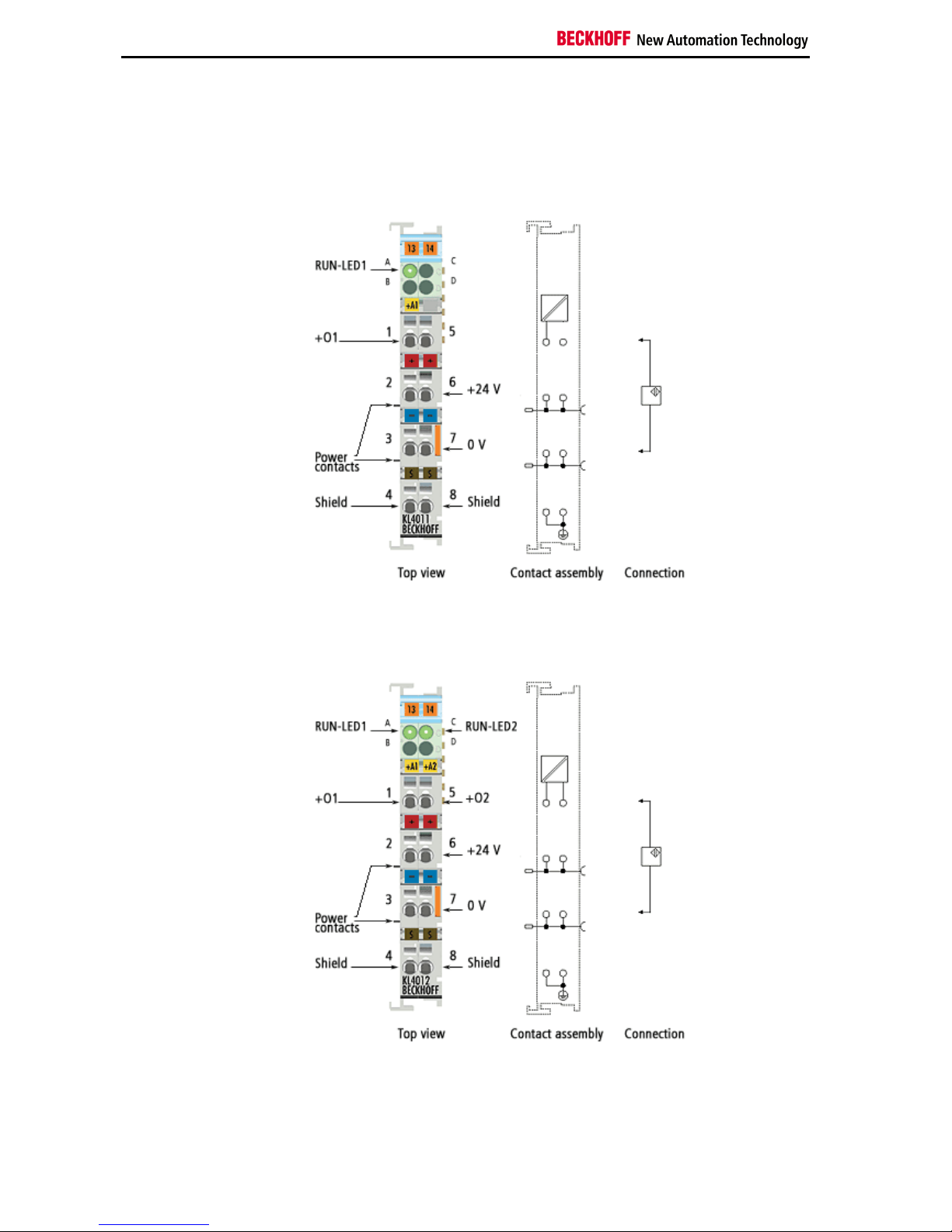
Connection
4 KL401x and KL402x
Connection
KL4011 and KL4021
KL4012 and KL4022
Page 7

Functional description
KL401x and KL402x 5
Functional description
The analog output terminals
- KL4011 and KL4012 generate signals in the range between 0 and 20 mA.
- KL4021 and KL4022 generate signals in the range between 4 and 20 mA.
with a resolution of 12 bits (4095 increments). The output current is
electrically isolated from the K-Bus.
The supply voltage fed in via the power contacts is used for generating the
output current.
Process data input format In the delivery state, the process data are entered in two's complement
form (integer -1 corresponds to 0xFFFF). Other formats may be selected
via the feature register.
Process data Output current
hexadecimal decimal KL4011, KL4012 KL4021, KL4022
0x0000 (0)
0 mA 4 mA
0x3FFF (16383)
10 mA 12 mA
0x7FFF (32767)
20 mA 20 mA
LED display Both RUN LEDs indicate the operating state of the associated terminal
channels.
Green LED: RUN
• On: normal operation
• Off: Watchdog-timer overflow has occurred. If no process data are
transmitted by the Bus Coupler for 100 ms, the green LEDs go out.
A user-specified voltage will be applied to the output (see feature
register).
Process data The process data arriving from the Bus Coupler are output to the process:
X = PLC process data
B_h, A_h = Manufacturer scaling (R19, R20)
B_w, A_w = User scaling (R33, R34)
Y_dac = output value to the D/A converter
Neither user nor manufacturer scaling are active:
Y_dac = X (1.0)
Manufacturer scaling active:
Y_1 = B_h + A_h * X (1.1)
Y_dac = Y_1
User scaling active:
Y_2 = B_w + A_w * X (1.2)
Y_dac = Y_2
Manufacturer and user scaling active:
Y_1 = B_h + A_h * X (1.3)
Y_dac = B_w + A_w * Y_1 (1.4)
The equations of the straight line are activated via register R32.
Page 8

Terminal configuration
6 KL401x and KL402x
Terminal configuration
The terminal can be configured and parameterised via the internal register
structure. Each terminal channel is mapped in the Bus Coupler. Depending
on the type of the Bus Coupler and the mapping configuration (e.g.
Motorola/Intel format, word alignment etc.) the terminal data are mapped in
different ways to the Bus Coupler memory. For parameterising a terminal,
the control and status byte also has to be mapped.
BK2000 Lightbus Coupler In the BK2000 Lightbus coupler, the control and status byte is mapped in
addition to the data bytes. This is always located in the low byte at the
offset address of the terminal channel.
Example for KL4012 and KL4022:
0
Offset Terminal1 Channel1 = 0
Offset Terminal2 Channel1 = 4
KL4022
Offset Terminal2 Channel2 = 8
User data allocation depending
on mapping
K-Bus
Beckhoff-Lightbus
bus coupler
BK2000
To the bus terminal
LH
C/S - 0
D0 - 0
D0 - 1
D1 - 0
D1 - 1
C/S - 1
C/S
C/S
Data LData H
Data H Data L
C/S
The terminal is
mapped in the
bus coupler.
BK3000 Profibus coupler For the BK3000 Profibus coupler, the master configuration should specify
for which terminal channels the control and status byte is to be inserted. If
the control and status byte are not evaluated, the terminals occupy 2 bytes
per channel:
• KL4011 and KL4021: 2 bytes of output data
• KL4012 and KL4022: 4 bytes of output data
Example for KL4012 and KL4022:
Offset Terminal1 Channel1 = 0
Offset Terminal1 Channel2 = 3
Offset Terminal2 Channel1 = 6
KL4022 Channel1
KL4022 Channel 2
The control-/status byte
must be inserted for
parametrization.
K-Bus
Profibus bus coupler
BK3000
To the bus terminal
Data H
Data L
D1 - 0
D0 - 0
D0 - 1
D1 - 1
C/S - 0
C/S
C/S - 1
0
The terminal is
mapped in the
bus coupler.
Page 9

Register Description
KL401x and KL402x 7
BK4000 Interbus Coupler The BK4000 Interbus Coupler maps the terminals in the delivery state with
2 bytes per channel:
• KL4011 and KL4021: 2 bytes of output data
• KL4012 and KL4022: 4 bytes of output data
Parameterisation via the fieldbus is not possible. If the control and status
byte is to be used, the KS2000 configuration software is required.
Example for KL4012 and KL4022:
Offset Terminal1 Channel1 = 0
Offset Terminal2 Channel1 = 4
Offset Terminal1 Channel2 = 2
Offset Terminal2 Channel1 = 6
The control/status byte
must be inserted for
parameterization (KS2000).
K-Bus
Interbus bus coupler
BK4000
To the bus terminal
D0 - 1
D0 - 0
Data H
Data H
Data H
D1 - 0
D1 - 1
Data L
Data L
0
The terminal is
mapped in the
bus coupler.
Other Bus Couplers and
further information
Further information about the mapping configuration of Bus Couplers can
be found in the Appendix of the respective Bus Coupler manual under
Master configuration.
i
Note
The Appendix contains an overview of possible mapping configurations
depending on the parameters that can be set.
Parameterisation with
KS2000
The parameterisations can be carried out independently of the fieldbus
system with the KS2000 configuration software via the serial configuration
interface in the Bus Coupler.
Register Description
Different operating modes or functionalities may be set for the complex
terminals. The General Description of Registers explains those register
contents that are the same for all complex terminals.
The terminal-specific registers are explained in the following section.
Access to the internal terminal registers is described in the Register
Communication section.
General Description of Registers
Complex terminals that possess a processor are able to exchange data bidirectionally with the higher-level controller. These terminals are referred to
below as intelligent Bus Terminals. These include analog inputs, analog
outputs, serial interface terminals (RS485, RS232, TTY etc.), counter
terminals, encoder interface, SSI interface, PWM terminal and all other
parameterisable terminals.
Page 10

Register Description
8 KL401x and KL402x
The main features of the internal data structure are the same for all the
intelligent terminals. This data area is organised as words and comprises
64 registers. The important data and parameters of the terminal can be
read and set through this structure. It is also possible for functions to be
called by means of corresponding parameters. Each logical channel in an
intelligent terminal has such a structure (4-channel analog terminals
therefore have 4 sets of registers).
This structure is divided into the following areas:
(A detailed list of all registers can be found in the Appendix.)
Register Application
0 to 7
Process variables
8 to 15
Type register
16 to 30
Manufacturer parameters
31 to 47
User parameters
48 to 63
Extended user area
Process variables
R0 to R7 Registers in the terminal's internal RAM:
The process variables can be used in addition to the actual process image.
Their function is specific to the terminal.
R0 to R5: Terminal-specific registers
The function of these registers depends on the respective terminal type
(see terminal-specific register description).
R6: Diagnostic register
The diagnostic register can contain additional diagnostic information. Parity
errors, for instance, that occur in serial interface terminals during data
transmission are indicated here.
R7: Command register
High-Byte_Write = function parameter
Low-Byte_Write = function number
High-Byte_Read = function result
Low-Byte_Read = function number
Type register
R8 to R15: Registers in the internal ROM of the terminal
The type and system parameters are hard programmed by the
manufacturer, and the user can read them but cannot change them.
R8: Terminal type
The terminal type in register R8 is needed to identify the terminal.
R9: Software version (X.y)
The software version can be read as a string of ASCII characters.
R10: Data length
R10 contains the number of multiplexed shift registers and their length in
bits.
The Bus Coupler sees this structure.
R11: Signal channels
Related to R10, this contains the number of channels that are logically
present. Thus for example a shift register that is physically present can
perfectly well consist of several signal channels.
R12: Minimum data length
The particular byte contains the minimum data length for a channel that is
to be transferred. If the MSB is set, the control and status byte is not
necessarily required for the terminal function and is not transferred to the
control, if the Bus Coupler is configured accordingly.
Page 11

Register Description
KL401x and KL402x 9
R13: Data type register
Data type register
0x00
Terminal with no valid data type
0x01
Byte array
0x02
Structure 1 byte n bytes
0x03
Word array
0x04
Structure 1 byte n words
0x05
Double word array
0x06
Structure 1 byte n double words
0x07
Structure 1 byte 1 double word
0x08
Structure 1 byte 1 double word
0x11
Byte array with variable logical channel length
0x12
Structure 1 byte n bytes with variable logical channel
length (e.g. 60xx)
0x13
Word array with variable logical channel length
0x14
Structure 1 byte n words with variable logical channel
length
0x15
Double word array with variable logical channel length
0x16
Structure 1 byte n double words with variable logical
channel length
R14: reserved
R15: Alignment bits (RAM)
The alignment bits are used to place the analog terminal in the Bus
Coupler on a byte boundary.
Manufacturer parameters
R16 to R30: Manufacturer parameter area (SEEROM)
The manufacturer parameters are specific for each type of terminal. They
are programmed by the manufacturer, but can also be modified by the
controller. The manufacturer parameters are stored in a serial EEPROM in
the terminal, and are retained in the event of voltage drop-out.
These registers can only be altered after a code-word has been set in R31.
User parameters
R31 to R47: User parameter area (SEEROM)
The user parameters are specific for each type of terminal. They can be
modified by the programmer. The user parameters are stored in a serial
EEPROM in the terminal, and are retained in the event of voltage drop-out.
The user area is write-protected by a code-word.
i
Note
R31: Code-word register in RAM
The code-word 0x1235 must be entered here so that parameters in the
user area can be modified. If any other value is entered into this register,
the write-protection is active. When write protection is not active, the code
word is returned when the register is read. If the write protection is active,
the register contains a zero value.
R32: Feature register
This register specifies the terminal's operating modes. Thus, for instance, a
user-specific scaling can be activated for the analog I/Os.
R33 to R47 Terminal-specific Registers
The function of these registers depends on the respective terminal type
(see terminal-specific register description).
Extended application region
R47 to R63
Extended registers with additional functions.
Page 12

Register Description
10 KL401x and KL402x
Terminal-specific register description
Process variables
R0 to R4: reserved
R5: Raw DAC value (Y_dac)
The 12-bit value transferred to the D/A converter is called raw DAC value.
It is calculated from the process data via the manufacturer and user
scaling.
R6 to R7: reserved
Manufacturer parameters
R17: Hardware compensation - offset
This register is used for hardware offset compensation (8-bit digital
potentiometer) of the terminal. The register is transferred to the hardware
after each processor reset or with each write access to R17. Note that the
transferred offset does not correspond to the DAC values.
High byte: reserved
Low byte: Offset value (0 to 255)
R18: Hardware compensation - gain
This register is used for hardware gain compensation (8-bit digital
potentiometer) of the terminal. The register is transferred to the hardware
after each processor reset or with each write access to R17.
High byte: reserved
Low byte: Gain value (0 to 255)
R19: Manufacturer scaling - offset (B_h)
16 bit signed integer [0x0000]
This register contains the offset of the manufacturer's equation of the
straight line (1.1). The straight-line equation is activated via register R32.
R20: Manufacturer scaling - gain (A_h)
16 bits signed integer *2-8 [0x0020]
This register contains the scale factor of the manufacturer's equation of the
straight line (1.1). The straight-line equation is activated via register R32.
1 corresponds to register value 0x0100.
R21: Manufacturer's switch-on value
[0V], 12 bits unsigned integer in X [0x000]
The manufacturer switch-on value is applied to the terminal output after a
system reset or a watchdog timer overflow (terminal has not received any
process data for 100 ms).
The manufacturer switch-on value is activated via register R32.
Page 13

Register Description
KL401x and KL402x 11
User parameters
R32: Feature register:
[0x0006]
The feature register specifies the operating modes of the terminal.
Feature bit
no.
Description of the operating mode
Bit 0
1 User scaling (1.2) active [0]
Bit 1
1 Manufacturer scaling (1.1) active [1]
Bit 2
1 Watchdog timer active [1]
In the delivery state, the watchdog timer is switched on.
In the event of a watchdog overflow, either the
manufacturer or the user switch-on value is applied to
the terminal output.
Bit 3
1 Sign / amount representation [0]
Bit 7...4
- reserved, do not change
Bit 8
0/1 0: Manufacturer switch-on value [0]
1: User switch-on value
Bit 15...9
- reserved, do not change
R33: User scaling - offset (B_w)
16 bit signed integer [0x0000]
This register contains the offset of the user straight-line equation (4.1). The
straight-line equation is activated via register R32.
R34: User scaling - gain (A_w)
16 bits signed integer * 2-8 [0x0100]
This register contains the scale factor of the user straight-line equation
(4.1). The straight-line equation is activated via register R32.
R35: User's switch-on value (Y_2)
16 bit signed integer [0x0000]
If the user switch-on value is activated in register R32, this value is applied
to the terminal output after a system reset or a watchdog timer overflow
(terminal has not received any process data for 100 ms).
Page 14

Register Description
12 KL401x and KL402x
Control and Status byte
Control byte for process
data exchange
Gain and offset
compensation
The control byte is transmitted from the controller to the terminal. It can be
used
- in register mode (REG = 1
bin
) or
- during process data exchange (REG = 0
bin
).
The control byte can be used to carry out gain and offset compensation for
the terminal (process data exchange). This requires the code word to be
entered in R31. The gain and offset of the terminal can then be
compensated.
The parameter will only be saved permanently once the code word is reset!
Control byte:
Bit 7 = 0
bin
Bit 6 = 1
bin
: Terminal compensation function is activated
Bit 4 = 1
bin
: Gain compensation
Bit 3 = 1
bin
: Offset compensation
Bit 2 = 0
bin
: Slower cycle = 1000 ms,
1
bin
: Fast cycle = 50 ms
Bit 1 = 1
bin
: up
Bit 0 = 1
bin
: down
Status byte for process
data exchange
The status byte is transmitted from the terminal to the controller. For model
KL4002, the status byte in the process data exchange is not used.
Register communication
Register access via
process data exchange
Bit 7 = 1
bin
: Register mode
If bit 7 of the control byte is set, then the first two bytes of the user data are
not used for exchanging process data, but are written into or read from the
terminal's register set.
Bit 6 = 0
bin
: read
Bit 6 = 1
bin
: write
Bit 6 of the control byte specifies whether a register should be read or
written. If bit 6 is not set, then a register is read out without modifying it.
The value can then be taken from the input process image.
If bit 6 is set, then the user data is written into a register. As soon as the
status byte has supplied an acknowledgement in the input process image,
the procedure is completed (see example).
Bit 0 to 5: Address The address of the register that is to be addressed is entered into bits 0 to
5 of the control byte.
Control byte in
register mode
MSB
REG=1 W/R
A5
A4
A3
A2
A1
A0
REG = 0
bin
: Process data exchange
REG = 1
bin
: Access to register structure
W/R = 0
bin
: Read register
W/R = 1
bin
: Write register
A5 to A0 = Register address
Address bits A5 to A0 can be used to address a total of 64 registers.
Page 15

Register Description
KL401x and KL402x 13
0
63
Terminal´s
register set
64 words
Control-/
status byte
User data
K-Bus
If control bit 7=0: input/output
If control bit 7=1:
registerconfiguration
C/S-bit 7
If control bit 7=1:
adress in the control bit 0-5
If control bit 6=0: read
If control bit 6=1: write
Complex bus terminal
To the bus coupler
HHL
L
2 or mors bytes
The control or status byte occupies the lowest address of a logical channel.
The corresponding register values are located in the following 2 data bytes.
(The BK2000 is an exception: here, an unused data byte is inserted after
the control or status byte, and the register value is therefore placed on a
word boundary).
Example 1 Reading of register 8 in the BK2000 with a KL4012 and the end terminal:
If the following bytes are transferred from the control to the terminal,
Byte
Byte 3 Byte 2 Byte 1 Byte 0
Name
DataOUT 1 DataOUT 0 Not used Control byte
Value
0xXX 0xXX 0xXX 0x88
the terminal returns the following type identifier (0x0FAC corresponds to
unsigned integer 4012).
Byte
Byte 3 Byte 2 Byte 1 Byte 0
Name
DataIN 1 DataIN 0 Not used Status byte
Value
0x0F 0xAC 0x00 0x88
Example 2 Writing of register 31 in the BK2000 with an intelligent terminal and the end
terminal:
If the following bytes (code word) are transferred from the control to the
terminal,
Byte
Byte 3 Byte 2 Byte 1 Byte 0
Name
DataOUT 1 DataOUT 0 Not used Control byte
Value
0x12 0x35 0xXX 0xDF
the code word is set, and the terminal returns the register address with bit
7 for register access as acknowledgement.
Byte
Byte 3 Byte 2 Byte 1 Byte 0
Name
DataIN 1 DataIN 0 Not used Status byte
Value
0x00 0x00 0x00 0x9F
Page 16

Appendix
14 KL401x and KL402x
Appendix
Mapping
As already described in the Terminal Configuration section, each Bus
Terminal is mapped in the Bus Coupler. In the delivery state, this mapping
occurs with the default settings of the Bus Coupler for this terminal. The
default setting can be changed with the KS2000 configuration software or
with a master configuration software (e.g. TwinCAT System Manager or
ComProfibus).
If the terminals are fully evaluated, they occupy memory space in the input
and output process image.
The following tables provide information about the terminal mapping,
depending on the conditions set in the Bus Coupler.
KL4011 and KL4021
Conditions Word offset High byte Low byte
Complete evaluation: no 0 Ch0 D1 Ch0 D0
Motorola format: no 1 - Word alignment: any 2 - -
Default mapping for:
CANopen, CANCAL,
DeviceNet, ControlNet,
Modbus, RS232, RS485
3 - Conditions Word offset High byte Low byte
Complete evaluation: no 0 Ch0 D0 Ch0 D1
Motorola format: yes 1 - Word alignment: any 2 - -
Default mapping for:
Profibus, Interbus
3 - Conditions Word offset High byte Low byte
Complete evaluation: yes 0 Ch0 D0 Ch0 CB/SB
Motorola format: no 1 - Ch0 D1
Word alignment: no 2 - 3 - -
Conditions Word offset High byte Low byte
Complete evaluation: yes 0 Ch0 D1 Ch0 CB/SB
Motorola format: yes 1 - Ch0 D0
Word alignment: no 2 - 3 - -
Conditions Word offset High byte Low byte
Complete evaluation: yes 0 res. Ch0 CB/SB
Motorola format: no 1 Ch0 D1 Ch0 D0
Word alignment: yes 2 - -
Default mapping for:
Lightbus, Ethernet,
Bus Terminal Controller
(BCxxxx)
3 - Conditions Word offset High byte Low byte
Complete evaluation: yes 0 res. Ch0 CB/SB
Motorola format: yes 1 Ch0 D0 Ch0 D1
Word alignment: yes 2 - 3 - -
Legend See mapping for KL4012 and 4022.
Page 17

Appendix
KL401x and KL402x 15
KL4012 and 4022
Conditions Word offset High byte Low byte
Complete evaluation: no 0 Ch0 D1 Ch0 D0
Motorola format: no 1 Ch1 D1 Ch1 D0
Word alignment: any 2 - -
Default mapping for:
CANopen, CANCAL,
DeviceNet, ControlNet,
Modbus, RS232, RS485
3 - Conditions Word offset High byte Low byte
Complete evaluation: no 0 Ch0 D0 Ch0 D1
Motorola format: yes 1 Ch1 D0 Ch1 D1
Word alignment: any 2 - -
Default mapping for:
Profibus, Interbus
3 - Conditions Word offset High byte Low byte
Complete evaluation: yes 0 Ch0 D0 Ch0 CB/SB
Motorola format: no 1 Ch1 CB/SB Ch0 D1
Word alignment: no 2 Ch1 D1 Ch1 D0
3 - -
Conditions Word offset High byte Low byte
Complete evaluation: yes 0 Ch0 D1 Ch0 CB/SB
Motorola format: yes 1 Ch1 CB/SB Ch0 D0
Word alignment: no 2 Ch1 D0 Ch1 D1
3 - -
Conditions Word offset High byte Low byte
Complete evaluation: yes 0 res. Ch0 CB/SB
Motorola format: no 1 Ch0 D1 Ch0 D0
Word alignment: yes 2 res. Ch1 CB/SB
Default mapping for:
Lightbus, Ethernet,
Bus Terminal Controller
(BCxxxx)
3 Ch1 D1 Ch1 D0
Conditions Word offset High byte Low byte
Complete evaluation: yes 0 res. Ch0 CB/SB
Motorola format: yes 1 Ch0 D0 Ch0 D1
Word alignment: yes 2 res. Ch1 CB/SB
3 Ch1 D0 Ch1 D1
Legend Complete evaluation:
The terminal is mapped with control and status byte.
Motorola format:
Motorola or Intel format can be set.
Word alignment:
The terminal is at word limit in the Bus Coupler.
Ch n SB: status byte for channel n (appears in the input process image).
Ch n CB: control byte for channel n (appears in the output process image).
Ch n D0: channel n, data byte 0 (byte with the lowest value)
Ch n D1: channel n, data byte 1 (byte with the highest value)
"-": This byte is not used or occupied by the terminal.
res.: reserved:
This byte occupies process data memory, although it is not used.
Page 18

Appendix
16 KL401x and KL402x
Register Table
These registers exist once for each channel.
Address Denomination Default
value
R/W Storage medium
R0
reserved 0x0000 R
...
... ... ... ...
R4
reserved 0x0000 R
R5
Raw DAC value variable R RAM
R6
Diagnostic register not used 0x0000 R
R7
Command register not used 0x0000 R
R8
Terminal type e.g. 4012 R ROM
R9
Software version number 0x???? R ROM
R10
Multiplex shift register 0x0218/0130 R ROM
R11
Signal channels 0x0218 R ROM
R12
Minimum data length 0x9800 R ROM
R13
Data structure 0x0000 R ROM
R14
reserved 0x0000 R
R15
Alignment register variable R/W RAM
R16
Hardware version number 0x???? R/W SEEROM
R17
Hardware compensation: Offset specific R/W SEEROM
R18
Hardware compensation: Gain specific R/W SEEROM
R19
Manufacturer scaling: Offset 0x0000 R/W SEEROM
R20
Manufacturer scaling: Gain 0x0020 R/W SEEROM
R21
Manufacturer's switch-on value 0x0000 R/W SEEROM
R22
reserved 0x0000 R/W SEEROM
...
... ... ... ...
R30
reserved 0x0000 R/W SEEROM
R31
Code word register variable R/W RAM
R32
Feature register 0x0006 R/W SEEROM
R33
User scaling: Offset 0x0000 R/W SEEROM
R34
User scaling: Gain 0x0100 R/W SEEROM
R35
User switch-on value 0x0000 R/W SEEROM
R36
reserved 0x0000 R/W SEEROM
...
... ... ... ...
R63
reserved 0x0000 R/W SEEROM
Page 19

Appendix
KL401x and KL402x 17
Support and Service
BECKHOFF and their partners around the world offer comprehensive service
and support, making available fast and competent assistance with all
questions related to BECKHOFF products and system solutions.
BECKHOFF Support
Support offers you comprehensive technical assistance, helping you not
only with the application of individual BECKHOFF products, but also with
other, wide-ranging services:
• world-wide support
• design, programming and commissioning of complex automation
systems
• and extensive training program for BECKHOFF system
components
Hotline: +49(0)5246/963-157
Fax: +49(0)5246/963-199
e-mail: support@beckhoff.com
BECKHOFF Service
The BECKHOFF Service Centre supports you in all matters of after-sales
service:
• on-site service
• repair service
• spare parts service
• hotline service
Hotline: +49(0)5246/963-460
Fax: +49(0)5246/963-479
e-mail: service@beckhoff.com
BECKHOFF company headquarters
Beckhoff Automation GmbH
Eiserstr. 5
D-33415 Verl
Germany
Phone: +49(0)5246/963-0
Fax: +49(0)5246/963-198
e-mail: info@beckhoff.com
The addresses of BECKHOFF's branch offices and representatives round the
world can be found on the internet pages:
http://www.beckhoff.com
You will also find further documentation for BECKHOFF components there.
 Loading...