


RS-485 Data Acquisition Module
Model 485SDA10
Document No. 485SDA103798
This product
Designed and Manufactured
In Ottawa, Illinois
USA
of domestic and imported parts by
B&B Electronics Mfg. Co. Inc.
707 Dayton Rd. -- P.O. Box 1040 -- Ottawa, IL 61350 PH (815) 433-5100 -- FAX (815) 434-7094
Internet: http://www.bb-elec.com sales@bb-elec.com support@bb.elec.com
© 1995 B&B Electronics -- Revised September 1998
485SDA103798 Manual |
Cover Page |
B&B Electronics -- 707 Dayton Rd. -- |
PO Box 1040 -- Ottawa, IL 61350 |
PH (815) 433-5100 -- |
FAX (815) 434-7094 |

Table of Contents |
|
|
Chapter 1- Introduction ........................................... |
|
1 |
485SDA10 Features ...................................................... |
|
1 |
Packing List ................................................................... |
|
2 |
Software Installation ...................................................... |
|
2 |
DOS ...................................................................................... |
|
2 |
Windows 3.11 ....................................................................... |
|
3 |
Windows 9x and Windows NT.............................................. |
|
3 |
Uninstall......................................................................... |
|
3 |
Windows 3.11 ....................................................................... |
|
3 |
Windows 9x & Windows NT ................................................. |
|
3 |
Getting Started .............................................................. |
|
3 |
485SDA10 Specifications .............................................. |
|
5 |
Analog to Digital Converter................................................... |
|
5 |
5 Volt Reference ................................................................... |
|
5 |
Digital Inputs ......................................................................... |
|
5 |
Digital Outputs ...................................................................... |
|
5 |
Power Supply........................................................................ |
|
5 |
Communications................................................................... |
|
5 |
Factory Default Settings ....................................................... |
|
5 |
Chapter 2 - Connections.......................................... |
|
6 |
A/D Connections............................................................ |
|
6 |
A/D Inputs #0-10................................................................... |
|
6 |
A/D Ref Input + ..................................................................... |
|
6 |
A/D Ref Input - ...................................................................... |
|
7 |
Analog Ground...................................................................... |
|
7 |
Typical Connections ............................................................. |
|
7 |
Digital I/O Connections .................................................. |
|
8 |
Digital Inputs #0-2................................................................. |
|
8 |
Digital Outputs #0-2 .............................................................. |
|
8 |
Digital Ground....................................................................... |
|
9 |
Typical Connections ............................................................. |
|
9 |
Serial Port Connections ............................................... |
|
10 |
Power Supply Connections.......................................... |
|
11 |
Chapter 3 - Commands.......................................... |
|
12 |
Syntax ......................................................................... |
|
13 |
Reading A/D Channels Command............................... |
13 |
|
Reading Digital I/O Command ..................................... |
|
15 |
Set Digital Output Command ....................................... |
|
16 |
Set Module Address Command ................................... |
16 |
|
Set Power-up States Command .................................. |
17 |
|
485SDA103798 Manual |
Table of Contents |
i |
B&B Electronics -- 707 Dayton Rd. -- PO Box 1040 -- Ottawa, IL 61350
PH (815) 433-5100 -- FAX (815) 434-7094

|
Set Turn-around Delay Command ............................... |
|
17 |
|
Read Module Configuration Command........................ |
17 |
|
Chapter 4 - A/D ....................................................... |
|
19 |
|
|
Sampling Rate............................................................. |
|
19 |
|
A/D Input Range .......................................................... |
|
19 |
|
Reference Inputs ......................................................... |
|
19 |
|
Data Range ................................................................. |
|
20 |
|
Converting Data........................................................... |
|
20 |
Chapter 5 - Software .............................................. |
|
22 |
|
|
Read A/D Command ................................................... |
|
22 |
|
Read Digital I/O Command.......................................... |
|
23 |
|
Set Digital Output States ............................................. |
|
24 |
|
Set Module Address .................................................... |
|
25 |
|
Set Power-up States Command .................................. |
|
26 |
|
Set Turn-around Delay ................................................ |
|
27 |
|
Read Module Configuration ......................................... |
|
28 |
Appendix A: Adding Data Field Confirmation.... |
A-1 |
||
Appendix B: Analog Input Impedance................ |
B-1 |
||
Appendix C: Decimal to HEX to ASCII Table .... |
C-1 |
||
Figures |
|
|
|
FIGURE 1.1 - 485SDA10 UNIT ...................................................................... |
|
1 |
|
FIGURE 1.2 - GENERAL BLOCK DIAGRAM ............................................... |
|
2 |
|
FIGURE 1.3 - A/D WITH VARIABLE RESISTOR ......................................... |
|
4 |
|
FIGURE 2.1 - TYPICAL 0-5V A/D CONNECTION ....................................... |
|
7 |
|
FIGURE 2.2 - TYPICAL DIGITAL I/O CONNECTIONS ............................... |
9 |
||
FIGURE 4.1 - A/D CONVERTER DATA RANGE........................................ |
|
20 |
|
FIGURE B-1 - EQUIVALENT INPUT CIRCUIT INCL/DRIVING SOURCEB-3 |
|||
Tables |
|
|
|
TABLE 2.1 - 485SDA10 I/O PORT PINOUT ...................................... |
|
8 |
|
TABLE 2.2 - RS-485 TERMINAL BLOCK CONNECTIONS .......... |
10 |
||
TABLE 3.1 - 485SDA10 COMMANDS ............................................. |
|
12 |
|
TABLE 3.2 - EQUIVALENT VALUES ............................................. |
|
13 |
|
TABLE 3.3 - READ A/D RESPONSE................................................ |
|
14 |
|
TABLE 3.4 - READ DIGITAL I/O RESPONSE FOR OUTPUTS..... |
15 |
||
TABLE 3.5 - READ DIGITAL I/O RESPONSE FOR INPUTS......... |
15 |
||
TABLE 3.6 - SET DIGITAL OUTPUT DATA BYTE VALUES ...... |
16 |
||
ii |
Table of Contents |
485SDA103798 Manual |
|
B&B Electronics -- 707 Dayton Rd. -- PO Box 1040 -- Ottawa, IL 61350
PH (815) 433-5100 -- FAX (815) 434-7094

TABLE 5.1 - DIGITAL I/O MASK VALUES.................................... |
24 |
TABLE A-1 EXTENDED COMMANDS........................................ |
A-2 |
TABLE C-1: DECIMAL TO HEX TO ASCII TABLE.................... |
C-1 |
485SDA103798 Manual |
Table of Contents |
iii |
B&B Electronics -- 707 Dayton Rd. -- PO Box 1040 -- Ottawa, IL 61350
PH (815) 433-5100 -- FAX (815) 434-7094

Chapter 1- Introduction
485SDA10 Features
The 485SDA10 is a general purpose control module which operates through an RS-485 interface. The 485SDA10 offers 11 channels of 10-bit A/D (analog to digital), 3 digital inputs and 3 digital outputs. With these features, the module can be used to sense a variety of external conditions and to control a variety of devices.
The 11 A/D channels allow you to measure voltages from 0 to 5 Volts. The 3 digital inputs and 3 digital outputs are CMOS/TTL compatible. The A/D and digital I/O lines are available through a DB25S (female) connector.
The 485SDA10 connects to the host computer’s RS-485 or RS-422 serial port using terminal blocks. The address and turnaround delays are software programmable to allow use of multiple devices or connection to existing systems. The unit automatically detects baud rates from 1200 to 9600. A data format of 8 data bits, 1 stop bit and no parity is used.
Configuration parameters are stored in non-volatile memory. The configuration parameters consist of the module address, communication turn-around delay, and digital output power-up states.
Figure 1.1 - 485SDA10 Unit
485SDA103798 Manual |
1 |
B&B Electronics -- 707 Dayton Rd. -- PO Box 1040 -- Ottawa, IL 61350
PH (815) 433-5100 -- FAX (815) 434-7094
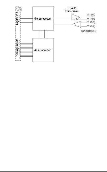
Figure 1.2 - General Block Diagram
Packing List
Examine the shipping carton and contents for physical damage. The following items should be in the shipping carton:
∙485SDA10 unit
∙One 485SDA10 3.5” disk
∙This instruction manual
∙RS-485/422 Application Note
If any of these items are damaged or missing contact B&B Electronics immediately.
Software Installation
The 485SDA10 comes with several useful programs such as a data logging utility, a demonstration program, etc. The installation for the SDA Logger is different depending on the platform you install it to. Please use the one appropriate to your system.
DOS
1.Place the disk in drive A.
2.Type A: and press the <ENTER> key.
3.Type INSTALL and press the <ENTER> key.
4.Follow the instructions given by the program.
2 |
485SDA103798 Manual |
B&B Electronics -- 707 Dayton Rd. -- PO Box 1040 -- Ottawa, IL 61350
PH (815) 433-5100 -- FAX (815) 434-7094

Windows 3.11
1.Insert SDA Logger installation disk in your floppy drive.
2.Click the File Manager button.
3.Select the floppy drive containing the SDA Logger installation disk.
4.Double click the Setup.exe icon when it appears.
5.Follow the installation instructions as prompted.
Windows 9x and Windows NT
1.Insert the SDA Logger installation disk in your floppy drive.
2.Click Start | Run.
3.Click the Browse button and choose the floppy drive containing the SDA Logger installation disk.
4.Double click the Setup.exe icon when it appears.
5.Click the OK button to run the Setup.exe program.
6.Follow the installation instructions as prompted.
Uninstall
Uninstall for the SDA Logger version is different for each Windows operating system. Below are the methods for uninstalling the SDA Logger.
Windows 3.11
1.Open the File Manager in the Control Panel.
2.Click the drive that SDA Logger was installed to.
3.Click the SDA16 directory.
4.Double click the UNWISE.EXE.
5.Follow the Uninstall Wizard.
Windows 9x & Windows NT
1.Open Start | Settings | Control Panel.
2.Open ADD/REMOVE PROGRAMS.
3.Click SDA LOGGER.
4.Click the Add/Remove button.
5.Follow the Uninstall Wizard.
Getting Started
This section will provide a quick example using the 485SDA10 and the demonstration program. If you experience any problems, refer to Chapter 2 for more precise information on connections. The demo program continually reads the A/D inputs and the digital I/O. The states of the digital outputs can be toggled using F2, F3, and F4. The serial port is configured for 9600 baud, 8 data bits, no parity, and 1 stop bit. The program supports standard addresses and IRQ’s for COM1 and COM2.
∙Connect a 0 to 5V DC analog device to A/D input #0, or you can connect a variable resistor as shown in Figure 1.3. The
485SDA103798 Manual |
3 |
B&B Electronics -- 707 Dayton Rd. -- PO Box 1040 -- Ottawa, IL 61350
PH (815) 433-5100 -- FAX (815) 434-7094

variable resistor must be greater than 1k Ohms to limit the output current to 5mA.
∙Connect A/D Ref Input+ to +5V DC.
∙Connect A/D Ref Inputto analog ground (See Figure 1.3).
∙Connect the 485SDA10 to an RS-422 or 4-wire RS-485 serial
port.
Once your connections have been made, run the demo program. Any change in A/D or digital lines on the 485SDA10 will automatically be displayed on the screen.
Figure 1.3 - A/D with Variable Resistor
4 |
485SDA103798 Manual |
B&B Electronics -- 707 Dayton Rd. -- PO Box 1040 -- Ottawa, IL 61350
PH (815) 433-5100 -- FAX (815) 434-7094
Analog to Digital Converter |
|
Resolution: |
10 bit |
Channels: |
11 |
Reference Range: |
5.0V DC max. (4.888 mV per bit) |
|
2.5V DC min. (2.444 mV per bit) |
A/D Ref. Input - |
0V DC to 2.5V DC |
A/D Ref. Input + |
2.5V DC to 5.0V DC |
Input Voltage Range: |
-0.3V DC to 5.3V DC |
Total Unadjusted Error: |
+/- 1 LSB max. |
A/D input channels must be driven from a source impedance less
than 1kΩ. |
|
5 Volt Reference |
|
Output Voltage: |
4.975 to 5.025V DC (5.0V DC typ.) |
Accuracy: |
+/- 0.5 % |
Output Current: |
5mA max. |
Digital Inputs |
|
Channels: |
3 |
Voltage Range: |
-30V DC to 30V DC |
Low Voltage: |
-30V DC to 1.0V DC |
High Voltage: |
2.0V DC to 30V DC |
Leakage Current: |
1 μA max. |
Digital Outputs |
|
Channels: |
3 |
Low Voltage: |
0.6V DC @ 8.7mA |
High Voltage: |
4.3V DC @ -5.4mA |
Power Supply |
|
Input Voltage: |
7V DC to 18V DC @ 30mA |
|
(Doesn’t include the power |
Communications |
consumption of external devices.) |
|
|
Standard: |
RS-422/485 |
Addresses: |
256 |
Turn-around Delay: |
Software programmable from 0 to 255 |
|
character transmission times. (1 char. |
|
trans. time @ 9600 baud = 1ms) |
Baud Rate: |
1200 to 9600 (automatic detection) |
Format: |
8 data bits, 1 stop bit, no parity |
Connector: |
DB-25S (female) |
Factory Default Settings |
|
Address: |
|
Turn-around Delay: |
|
|
Power-up States: |
|
|
485SDA10 Specifications |
|
|
|
ACSII “0” (48 decimal or 30h) |
|
|
1 |
|
|
0 |
|
|
|
|
485SDA103798 Manual |
|
5 |
B&B Electronics -- 707 Dayton Rd. -- PO Box 1040 -- Ottawa, IL 61350
PH (815) 433-5100 -- FAX (815) 434-7094

Chapter 2 - Connections
This chapter will cover the connections required for the 485SDA10. There are four sets of connections:
∙A/D converter
∙Digital I/O
∙Serial port
∙Power supply
Do not make any connections to the 485SDA10 until you have read this chapter.
CAUTION: When making electrical connections it is important to power down the devices being connected. If this is not possible, precautions must be taken to ensure electrical specifications are not exceeded.
NOTE: If you do not intend to use a section (A/D or I/O), it is still important to read each one.
A/D Connections
The A/D connections are made on the I/O port, which is a DB25S (female) connector. Table 2.1 shows the pinout of the I/O port. The next sections explain the functions and connections for the various analog signals.
A/D Inputs #0-10
These are the analog input channels. The analog data that is read from the 485SDA10 is related to the voltage on these pins. Connect your devices to the analog input channels. Voltages on these inputs must remain between 0 and 5.0V DC. Connect unused A/D inputs to analog ground.
A/D Ref Input +
The voltage connected to this pin determines the upper end of the input voltage range. For proper operation, this pin must be connected to a DC voltage between +2.5 and +5.0 Volts. The 485SDA10 provides a 5.0V +/-0.5% reference on pin 17. The 5V reference can be used if you require a 0 to 5V DC input range. If your application requires a better reference voltage or a different input range, you must supply the appropriate reference to the A/D Ref Input+ pin. This voltage must be at least 2.5V greater
than A/D Ref Input-. Bypassing the A/D Ref Input+ pin with 0.01μF ceramic and 10μF tantalum capacitors to analog ground will decrease noise levels.
6 |
485SDA103798 Manual |
B&B Electronics -- 707 Dayton Rd. -- PO Box 1040 -- Ottawa, IL 61350
PH (815) 433-5100 -- FAX (815) 434-7094
A/D Ref Input -
The voltage connected to this pin determines the low end of the input voltage range. For proper operation, this pin must be connected to a DC voltage between 0 and +2.5 Volts. Typically, this is connected to your device’s ground and analog ground (0V).
Analog Ground
This pin should be connected to your analog device’s ground. If ground (0V) is the low end of your input voltage range,
A/D Ref Inputshould be connected to this pin. To minimize noise, do not connect analog ground and digital ground together. Connect unused A/D inputs to analog ground.
Typical Connections
Figure 2.1 shows the typical connections of the 485SDA10 for a 0 to 5V DC input range.
Figure 2.1 - Typical 0-5V A/D Connection
485SDA103798 Manual |
7 |
B&B Electronics -- 707 Dayton Rd. -- PO Box 1040 -- Ottawa, IL 61350
PH (815) 433-5100 -- FAX (815) 434-7094

Digital I/O Connections
The digital I/O connections are made on the I/O port, which is a DB-25S (female) connector. Table 2.1 shows the pinout of the I/O port. The next sections explain the functions and connections for the various digital signals.
Table 2.1 - 485SDA10 I/O Port Pinout
DB-25S |
|
|
DB-25S |
|
Pin # |
Function |
|
Pin # |
Function |
|
|
|
|
|
1 |
GND |
|
14 |
Digital Output #0 |
2 |
+12V DC Output* |
|
15 |
Digital Output #1 |
3 |
Digital Input #0 |
|
16 |
Digital Output #2 |
4 |
Digital Input #1 |
|
17 |
+5V DC Output |
5 |
Digital Input #2 |
|
18 |
A/D Ref. Input + |
6 |
Digital GND |
|
19 |
A/D Ref. Input - |
7 |
Analog GND |
|
20 |
No connection |
8 |
A/D Input #0 |
|
21 |
A/D Input #6 |
9 |
A/D Input #1 |
|
22 |
A/D Input #7 |
10 |
A/D Input #2 |
|
23 |
A/D Input #8 |
11 |
A/D Input #3 |
|
24 |
A/D Input #9 |
12 |
A/D Input #4 |
|
25 |
A/D Input #10 |
13 |
A/D Input #5 |
|
|
|
*Actual output is equal to power supply input minus 0.7V DC
Digital Inputs #0-2
The digital input lines are CMOS/TTL compatible and can handle voltages from -30V DC to +30V DC. If a digital input is from -30V DC to 1.0V DC, the state will be read as a “0” (LOW). If a digital input is from 2.0V DC to 30V DC, the state will be read as a “1” (HIGH). Connect unused digital inputs to digital ground.
Digital Outputs #0-2
The digital output lines are CMOS/TTL compatible. A digital output that is set to a “0” (LOW) will output a voltage from 0 to 0.6V DC. A digital output that is set to a “1” (HIGH) will output a voltage from 4.3V DC to 5.0V DC. Refer to Chapter 1, Specifications, for more information. Unused digital output lines should be left open.
8 |
485SDA103798 Manual |
B&B Electronics -- 707 Dayton Rd. -- PO Box 1040 -- Ottawa, IL 61350
PH (815) 433-5100 -- FAX (815) 434-7094
 Loading...