AVER AL251, AL250 Datasheet

AL250/251 Data Sheets

AL250
Contents
1.0 Features ___________________________________________________________________ 3
2.0 Applications ________________________________________________________________ 3
3.0 General Description__________________________________________________________ 4
4.0 Pinout Diagrams ____________________________________________________________ 5
5.0 Pin Definition and Description _________________________________________________ 6
6.0 Functional Description _______________________________________________________ 8
6.1 Digital Input/Output Data Formats __________________________________________________8
6.2 Default Resolution________________________________________________________________9
6.3 Video Timing ____________________________________________________________________9
6.4 Border/Border Color ____________________________________________________________13
6.5 OSD Interface __________________________________________________________________14
6.6 External Overlay________________________________________________________________15
6.7 Look-up Table (LUT) ____________________________________________________________16
6.8 I2C Programming _______________________________________________________________16
6.9 Video Decoding _________________________________________________________________18
7.0 Electrical Characteristics ____________________________________________________ 20
7.1 Recommended Operating Conditions _______________________________________________20
7.2 Characteristics__________________________________________________________________20
8.0 AL250/251 Register Definition________________________________________________ 22
8.1 Register Description _____________________________________________________________23
9.0 Board Design and Layout Considerations _______________________________________ 29
9.1 Grounding _____________________________________________________________________29
9.2 Power Planes and Power Supply Decoupling _________________________________________29
9.3 Digital Signal and Clock Interconnect _______________________________________________29
9.4 Analog Signal Interconnect________________________________________________________29
10.0 Mechanical Drawing_______________________________________________________ 30
11.0 Power Consumption _______________________________________________________ 32
July 28, 1999 2

AL250/251 Video Scan Doubler
1.0 Features
• Convert interlaced TV signal (NTSC/PAL) into
non-interlaced RGB format for CRT monitors
or LCD panels
• Highly integrated design with built-in DAC,
SRAM, OSD and LUT
• Built-in on-screen-display with programmable
bitmap
• Interpolated scan doubling with no tearing or
jagged edge artifacts
• Reduced interlace flicker
• Auto NTSC/PAL detect
• Digital video input of square pixel, ITU-RBT
601 (CCIR 601), or user-defined format
• Analog/digital non-interlaced RGB (VGA)
signal output (Scan Doubled or Deinterlaced)
• I2C programming interface
• Power-down control via I2C
AL250
• Internal RGB video lookup table (LUT) to
provide gamma correction and special effects
• Overlay support for title making and complex
on-screen display
• Self-initialization without software (Plug &
Play)
• 3.3 or 5 volt support
• 16-bit digital RGB/YUV output (AL251 only)
2.0 Applications
• TV-ready Multimedia Computer Monitor
• TV to PC Video Scan Converter Box
• Progressive Scan TV
• Video Game Station
• DVD Player
• LCD TV Monitor
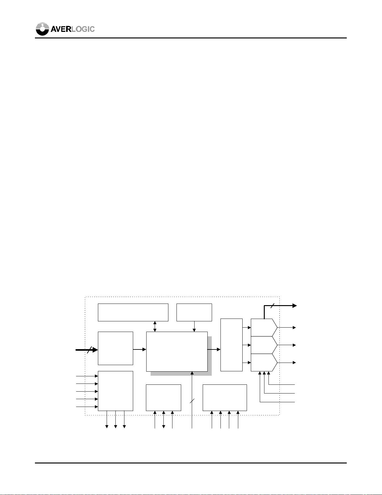
Digital
YUV or RGB
input
VCLK
VCLKX2
VIDHS
VIDVS
HREF
16
Video Memory
Video
Formatter
Timing
Control
GVS
GHS
GHREF
On-screen
Display
Video Processor
and Scan Doubler
I2C Circuit
2
SCL
SDA
CADDR
2
I
OVLCTRL
RGB
Video
Lookup
Tables
Mode Control
STD
RESET
INTYPE
8-bit DAC
8-bit DAC
8-bit DAC
SQUARE
16
AL250-01
Digital YUV or
RGB output
(AL251)
R
G
B
RSET
VREF
COMP
July 28, 1999 3

AL250
3.0 General Description
The AL250/251 Video Scan Doubler (De-Interlacer) is a video conversion chip for consumer video
and multimedia applications. It converts interlaced NTSC or PAL, ITU-RBT 601 (CCIR 601) or
square pixel, YUV422 or RGB565 digital signals into computer monitor RGB signals for direct
connection to a computer monitor or progressive scan TV.
By using I2C interface control, the AL250/251 can also be programmed to co-ordinate with various
input resolutions, adjust screen positioning and crop video noise from around the original input video
boundary.
The internal RGB video lookup tables (LUT), which are controlled via I2C interface, can provide
gamma correction for calibrating the color accuracy of different types of CRT’s and improving the
contrast level to display more vivid pictures.
A built-in on-screen-display (OSD) provides programmable bitmap RAM for custom design icons and
on-screen control panels.
Overlay function is supported to create titling or on-screen-display menus for video adjustment.
The AL251 provides all the features of the AL250. Additionally, it has digital output in YUV422 or
RGB565 format, and can convert NTSC video for VGA LCD panels.
The AverLogic proprietary digital signal processing technology creates a highly stable video image
without tearing effects or jagged edges. The output picture is smoother and has less flicker than the
original input signal/picture.
July 28, 1999 4

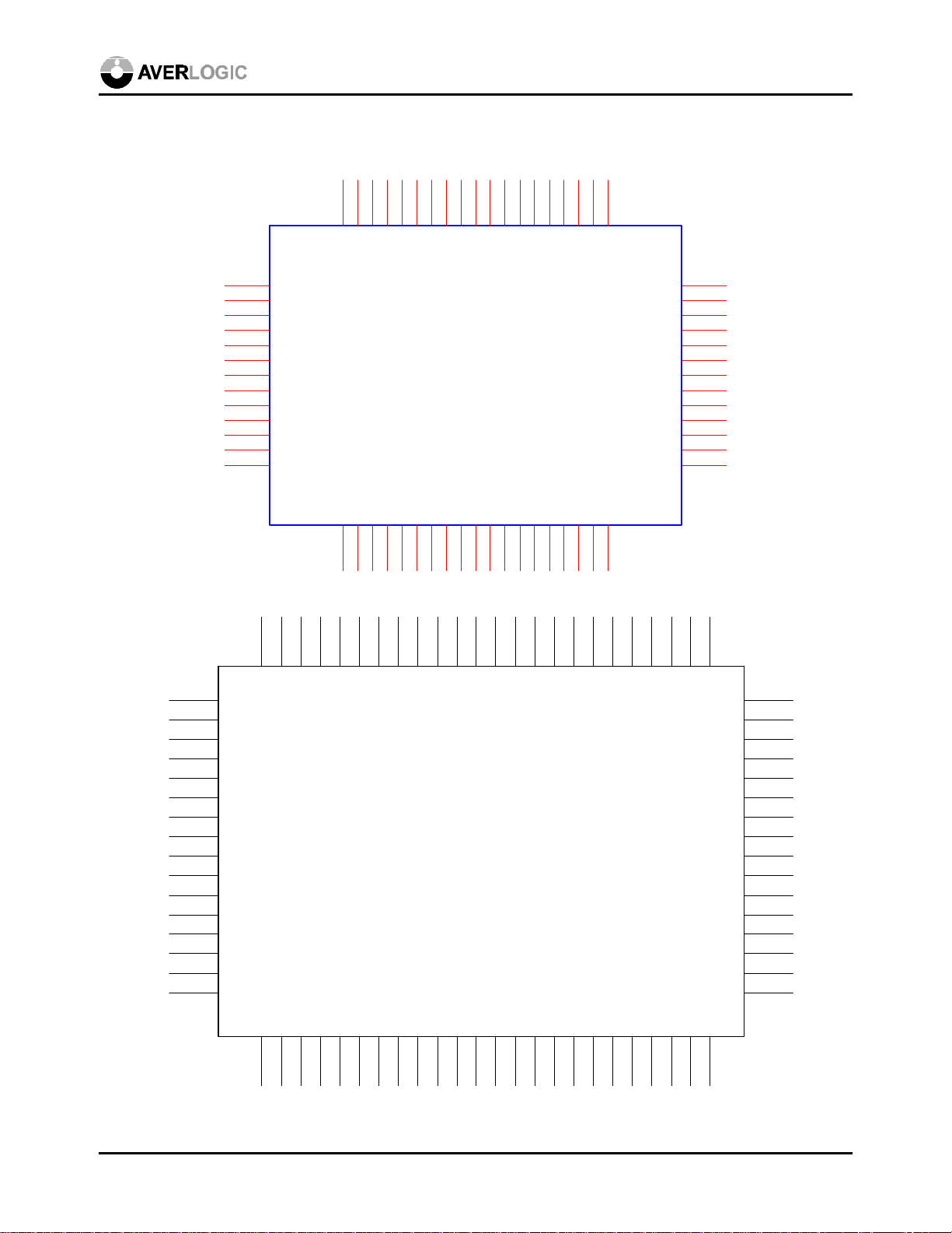
4.0 Pinout Diagrams
10
11
12
13
14
15
16
17
18
19
52
VDIN5
53
VDIN6
54
VDIN7
55
VDIN8
56
VDD
57
VDIN9
58
VDIN10
59
VDIN11
60
GND
61
VDIN12
62
VDIN13
63
VDIN14
64
VDIN15
51
50
VDIN4
VIDHS
49
48
VDIN3
VDIN2
VDD
VCLK
47
46
45
44
42
VDD43VDD
GND
VDIN1
VDIN0
TESTY7
TESTY6
AL250
VIDVS
VCLKX2
HREF
GND
STD0
STD1
41
40
TESTY5
INTYPE
GND
39
38
37
TESTY4
TESTY3
TESTY2
TESTIN
I2CADDR
SQUARE
36
35
34
TESTY1
TESTY0
OVLCTRL1
VDD
/RESET
SDA
33
GND
VREF
OVLCTRL0
COMP
RSET
AVDD
AGND
AG
AVDD
AB
AGND
GHS
GVS
GREF
SCL
VDD
AR
AL250
32
31
30
29
28
27
26
25
24
23
22
21
20
1
2
3
4
5
6
7
8
9
64636261605958
65
66
67
68
69
70
71
72
73
74
75
76
77
78
79
80
DO14
DO15
VDIN5
VDIN6
VDIN7
VDIN8
VDD
VDIN9
VDIN10
VDIN11
GND
VDIN12
VDIN13
VDIN14
VDIN15
NC
DO13
DO12
VDIN4
VDIN3
VDIN2
VDIN1
565554535251504948474645444342
57
DO5
DO4
DO3
DO2
GND
VDIN0
DO7
DO6
VDD
VDD
DO1
DO0
OVLCTRL1
AL251
GND
OVLCTRL0
41
NCNCNC
NC
VREF
COMP
RSET
AVDD
AR
AGND
AG
AVDD
AB
AGND
GHS
GVS
GREF
D011
D010
40
39
38
37
36
35
34
33
32
31
30
29
28
27
26
25
NC1NC2VIDHS3VDD4VCLK5VIDVS6GND7VCLKX2
NC
8
HREF9STD010STD111GND12INTYPE13SQUARE14TESTIN15I2CADDR16/RESET17SDA18VDD19SCL20VDD21DO822DO9
23
24
AL251-01 pinout diagram
July 28, 1999 5

5.0 Pin Definition and Description
Symbol Type 250 Pin # 251 Pin # Description
Video Interface
AL250
VDIN (15 to 0) in (CMOS) 64-61, 59-
57, 55-52,
51-47
VCLK in (CMOS) 3 6 Video clock input
VCLKX2 in (CMOS) 6 9 2 times of video clock input
VIDHS in (CMOS) 1 4 Horizontal sync. input signal
VIDVS in (CMOS) 4 7 Vertical sync. input signal
HREF in (CMOS) 7 10 Horizontal reference input signal; this signal is
Graphic Interface
RSET In (100 ohm) 30 37 Full Scale Current Adjust; 100 ohm pull-down
VREF in (1.235V) 32 39 Voltage Reference Input
COMP
AR out (0.7V) 28 35 VGA analog red output
out (0.1µF)
31 38
79-76, 7472, 70-67,
62-58
Digital video data input. Please refer to the input
data format table for details
used to indicate data on the digital YUV bus. The
positive slope marks the beginning of a new
active line.
Compensation pin; 0.1µF pull-up
AG out (0.7V) 26 33 VGA analog green output
AB out (0.7V) 24 31 VGA analog blue output
DO (15 to 0) out (CMOS) N/A 66-63, 26-
23, 56-55,
52-47
GHS out (TTL) 22 29 VGA horizontal sync. output signal
GVS out (TTL) 21 28 VGA vertical sync. output signal
GHREF out (CMOS) 20 27 VGA horizontal reference output signal; it can be
Reset & Mode Select
/RESET in (CMOSd) 15 18 Reset input; active low
STD (1 to 0) in (CMOSd) 9, 8 12, 11 Video Input Standard select
Digital YUV422 or RGB565 output, selected by
register 08h <7>
used to indicate blanking interval.
00: NTSC input
July 28, 1999 6

AL250
01: PAL input
10: Automatic standard detection
11: Reserved for testing
INTYPE in (CMOSd) 11 14 Input video data format select
0: 422 YUV (16-bit)
1: 565 RGB (16-bit)
SQUARE in (CMOSd) 12 15 Square pixel/YUV (CCIR-601) input select
0: YUV (CCIR-601)
1: Square pixel
TESTIN in (CMOSd) 13 16 Test input pin, to be pulled high for normal
applications.
I2C & overlay Interface
SCL in (CMOSsu) 18 21 I2C-bus serial clock input
SDA in/out
(CMOSsu)
I2CADDR in (CMOSd) 14 17 I2C -bus slave address select
OVLCTRL
(1 to 0)
Test pins
TESTY
(7 to 0)
Power & Ground Pins
VDD power 2, 17, 19,
GND power 5, 10, 33,
in (CMOSd) 35, 34 46, 45 Overlay control
out (CMOS) 45-44,
16 19 I2C -bus serial data input/output
0: write address = 58, read address = 59
1: write address = 5C, read address = 5D
00: No overlay
01: Overlay color #1
10: Overlay color #2
11: Overlay color #3
Overlay colors can be programmed by software
N/A Test output pins, for factory test only
41-36
42, 43, 56
46, 60
5, 20, 22,
53, 54, 71
8, 13, 44,
57, 75
Digital power pins. Connected to +5V power
Digital ground pins
AVDD power 25, 29 32, 36 Analog power pins. Connected to +5V power
AGND power 23, 27 30, 34 Analog ground pins
Notes:
CMOSd : CMOS with internal pull-down
CMOSsu : CMOS with Schmitt trigger and internal pull-up
July 28, 1999 7

AL250
6.0 Functional Description
6.1 Digital Input/Output Data Formats
The digital video data formats that the AL250/251 accepts are YUV422 and RGB565. The pin
definition and the RGB 888 to 565 mapping is as follows:
Video Data Signal
VDIN15
VDIN14
VDIN13
VDIN12
VDIN11
VDIN10
VDIN9
VDIN8
VDIN7
VDIN6
VDIN5
VDIN4
VDIN3
VDIN2
Pin Number
AL250 AL251
64 79
63 78
62 77
61 76
59 74
58 73
57 72
55 70
54 69
53 68
52 67
51 62
50 61
49 60
YUV 422 RGB 888→565
Y7 R7
Y6 R6
Y5 R5
Y4 R4
Y3 R3
Y2 G7
Y1 G6
Y0 G5
U7, V7 G4
U6, V6 G3
U5, V5 G2
U4, V4 B7
U3, V3 B6
U2, V2 B5
VDIN1
VDIN0
Pixel clock
INTYPE select INTYPE = 0 INTYPE = 1
48 59
47 58
- -
U1, V1 B4
U0, V0 B3
VCLK VCLK
To select YUV422 or RGB565 as the input format, program the Board Configuration Register #02h,
or set the hardware pin “INTYPE” (AL250 pin#11, AL251 pin#14).
The AL251 provides digital output in RGB565 or YUV422 format. The pin definition and the
RGB565 to 888 mapping is as follows:
Video Data Signal AL251 Pin # YUV 422 RGB 565→888
DO7 56 Y7 R7
DO6 55 Y6 R6
July 28, 1999 8

DO5 52 Y5 R5
DO4 51 Y4 R4
DO3 50 Y3 R3
DO2 49 Y2 G7
DO1 48 Y1 G6
DO0 47 Y0 G5
DO15 66 U7, V7 G4
DO14 65 U6, V6 G3
DO13 64 U5, V5 G2
DO12 63 U4, V4 B7
DO11 26 U3, V3 B6
DO10 25 U2, V2 B5
DO9 24 U1, V1 B4
DO8 23 U0, V0 B3
OutFormat select - 1 0
AL250
To select YUV422 or RGB565 as the output format, program the Control Register #08h<7>, i.e.,
OutFormat.
6.2 Default Resolution
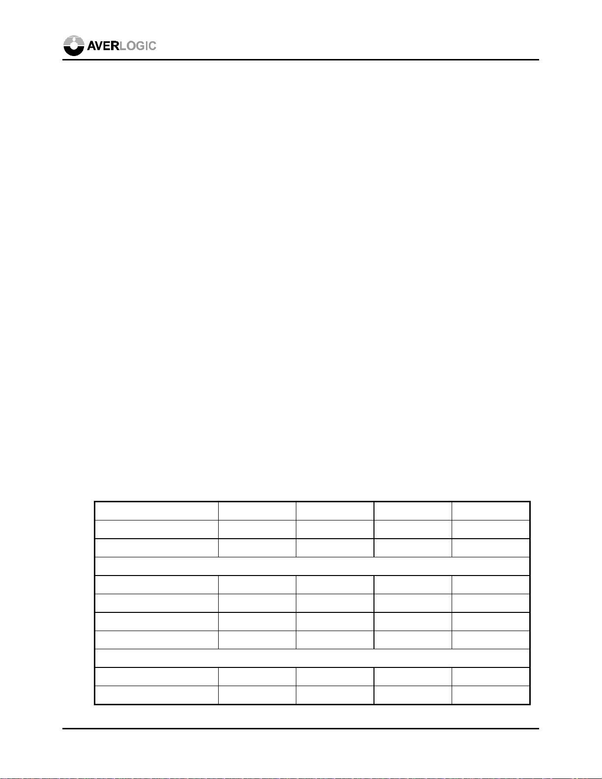
The resolution of the AL250/251 applications depends on the input video source, e.g., the digital
video decoder. The typical resolution of the video decoder that the AL250/251 supports without
software, and the VCLK frequency provided by the decoder to the AL250/251 is as follows:
Square Pixel CCIR 601
NTSC PAL NTSC PAL
Pixel Total 780 x 525 944 x 625 858 x 525 864 x 625
Pixel Active 640 x 480 768 x 576 720 x 480 720 x 576
VCLKx2 (MHz) 24.545454 29.5 27 27
VCLK (MHz) 12.272727 14.75 13.5 13.5
The AL250/251 can process up to 768 active pixels per line and 1024 lines per frame.
6.3 Video Timing
The AL250/251 registers 20h~29h and 2Bh~2Eh are used to control the video timing. All increments
are either by 8 pixels per line or by 4 lines per frame. All values (times 8 or 4) are relative to the input
July 28, 1999 9

AL250
video source H-sync or V-sync. These registers need to be programmed if the input video resolution
is different from the default resolution supported.
The H-sync Start and End (registers 22h and 23h) define the output horizontal sync period relative to
the input H-sync leading edge.
The Horizontal Blank Start and End (registers 2Bh and 2Ch) define the output H-sync blanking
period.
The Horizontal Capture Start and End (registers 20h and 21h) define the active pixels in each line
relative to the input video H-sync. These registers can also be used for adjusting the position of the
output picture.
The Horizontal Total High and Low (registers 24h and 29h) define the total number of pixels per line.
The AL250/251 can detect the H-total automatically when the input data is of the typical resolution
mentioned in the Default Resolution section.
The V-sync Start and End (registers 27h and 28h) define the output V-sync period relative to the input
V-sync start.
The Vertical Blank Start and End (registers 2Dh and 2Eh) define the output V-sync blanking period.
The Vertical Capture Start and End (registers 25h and 26h) define the active lines.
The total number of lines per frame (Vertical Total) is detected by the AL250/251 automatically.
To take advantage of the auto detection of the AL250/251, set the bit 3 of the Control register #08h
(Softtime) as 0. If a user-defined input format is used, then disable the hardware default by setting this
bit as 1, and write all of the parameters to the corresponding registers to define the format. The
sample code the AL250EVB provides disables the hardware settings.
The following typical parameters (as well as hardware default values) are for reference:
Mode Square NTSC Square PAL CCIR NTSC CCIR PAL
H(Horizontal) total 780 944 858 864
V(Vertical) total 525 625 525 625
HDE Start 120 160 72 80
HDE End 736 896 752 760
H-sync Start 776 0 792 808
H-sync End 56 72 856 16
VDE Start 48 60 48 60
VDE End 500 604 500 604
July 28, 1999 10
 Loading...