


Global LCD Panel Exchange Center |
www.panelook.com |
To Matsushita Electric Group |
Date of issue: Jun. 5th, 2006 |
DELIVERY SPECIFICATIONS
Product Description: |
T315XW02 V2 |
Part Number: |
97.31T03.200 |
Matsushita Global Part Number: |
L5EDD8Q00023 |
Matsushita Issue Number: |
L20060185 |
Supplier: |
Customer: |
Approved by: PL Chen 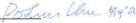
Reviewed by: Hong Jye Hong
Prepared by: Jacky Su 
©Copyright AU Optronics, Inc. |
|
|
January, 2003 All Rights Reserved. |
T315XW02 V2 - Specs. Ver 0.6 |
1/31 |
No Reproduction and Redistribution Allowed |
|
|
One step solution for LCD / PDP / OLED panel application: Datasheet, inventory and accessory! www.panelook.com

Global LCD Panel Exchange Center |
www.panelook.com |
Document Version : 0.6
Date : 2006/07/17

 Product Specifications
31.5” WXGA Color TFT-LCD Module
 Model
Model Name: T315XW02 V2
( ) Preliminary Specifications
(*) Final Specifications
©Copyright AU Optronics, Inc. |
|
|
January, 2003 All Rights Reserved. |
T315XW02 V2 - Specs. ver 0.6 |
2/31 |
No Reproduction and Redistribution Allowed |
|
|
One step solution for LCD / PDP / OLED panel application: Datasheet, inventory and accessory! www.panelook.com

Global LCD Panel Exchange Center |
www.panelook.com |
Contents
No
COVER
CONTENTS
RECORD OF REVISIONS
1 GENERAL DESCRIPTION
2 ABSOLUTE MAXIMUM RATINGS
3 ELECTRICAL SPECIFICATIONS
3-1 ELECTRICAL CHARACTREISTICS
3-2 INTERFACE CONNECTIONS
3-3 SIGNAL TIMING SPECIFICATIONS
3-4 SIGNAL TIMING WAVEFORMS
3-5 COLOR INPUT DATA REFERNECE


3-6 POWER SEQUENCE
4OPTICAL SPECIFICATIONS
5MECHANICAL CHARACTERISTICS
6RELIABLITY 

7 INTERNATIONAL STANDARDS
7-1  SAFETY
7-2 EMC
8PACKING
9PRECAUTIONS
©Copyright AU Optronics, Inc. |
|
|
January, 2003 All Rights Reserved. |
T315XW02 V2 - Specs. ver 0.6 |
3/31 |
No Reproduction and Redistribution Allowed |
|
|
One step solution for LCD / PDP / OLED panel application: Datasheet, inventory and accessory! www.panelook.com

Global LCD Panel Exchange Center |
www.panelook.com |
Record of Revision
Version |
Date |
No |
|
Old Description |
|
|
New Description |
Remark |
||||||
|
|
|
|
|
|
|
|
|
|
|
|
|
|
|
0 |
2006/1/20 |
|
First issue |
|
|
|
|
|
|
|
|
|
|
|
|
|
|
|
|
|
|
|
|
|
|||||
0.1 |
2006/3/31 |
3-1 |
Backlight |
Power |
consumption: |
101 |
Backlight Power consumption: 100 |
Value |
update |
|||||
|
|
|
|
|
|
|
|
|
||||||
|
|
3-2 |
Electrical |
specification- |
|
Electrical specification- |
Value |
update |
||||||
|
|
|
VBLON, On=3V (Min) |
|
VBLON, On=2V (Min) |
|
|
|||||||
|
|
|
|
|
|
|
|
|
||||||
|
|
3-2 |
Electrical |
specification- |
|
Electrical specification- |
Value |
update |
||||||
|
|
|
V_PWM(Max)=3V (Min) |
|
V_PWM(Max)=2V (Min) |
|
|
|||||||
|
|
|
|
|
|
|
|
|
||||||
|
|
3-2 |
Electrical |
specification- |
|
Electrical specification- |
Value |
update |
||||||
|
|
|
External PWM Duty Ratio, |
|
External PWM Duty Ratio, |
|
|
|||||||
|
|
|
D_EPWM: 50(Min), 100(Max) |
|
D_EPWM: 30(Min), 100(Max) |
|
|
|||||||
|
|
|
|
|
|
|
|
|
||||||
|
|
3-2 |
Electrical |
specification- |
|
Electrical specification- |
Value |
update |
||||||
|
|
|
External PWM Frequency, |
|
External PWM Frequency, |
|
|
|||||||
|
|
|
F_EPWM: 120(Min), 240(Max) |
|
F_EPWM: 150(Min), 300(Max) |
|
|
|||||||
|
|
|
|
|
|
|
|
|
||||||
|
|
3.6.2 |
Power Sequence |
for Inverter |
|
Power Sequence for Inverter with |
Figure |
and |
||||||
|
|
|
|
|
|
|
|
|
|
new figure and parameters |
value |
update |
||
|
|
|
|
|
|
|
|
|
||||||
0.2 |
2006/4/07 |
3-1 |
Backlight |
Power |
consumption: |
100 |
Backlight Power consumption: 92 |
Value update |
||||||
|
|
|
|
|
|
|
|
|
|
(Typ.), |
101(Max.) |
|
|
|
|
|
|
|
|
|
|
|
|
|
|
|
|||
|
|
3-2 |
Input |
Current: |
4.1 |
|
Input |
Current(Turn |
On Condition): |
|
|
|||
|
|
|
Input |
Power: |
100 |
|
3.7(Min.), 4.1(Typ.), |
4.5(Max.) |
|
|
||||
|
|
|
|
|
|
|
|
|
|
Input Current (Stable Condition): |
|
|
||
|
|
|
|
|
|
|
|
|
|
3.45(Min.), 3.8(Typ.), 4.15(Max.) |
|
|
||
|
|
|
|
|
|
|
|
|
|
Input Power (Turn On Condition): |
|
|
||
|
|
|
|
|
|
|
|
|
|
100(Typ.), 110(Max.) |
|
|
|
|
|
|
|
|
|
|
|
|
|
|
Input Power (Stable Condition): |
|
|
||
|
|
|
|
|
|
|
|
|
|
92(Typ.), 101(Max.) |
|
|
|
|
|
|
|
|
|
|
|
|
|
||||||
0.3 |
2006/5/11 |
3 |
Inverter Pin |
assignment: |
|
Inverter Pin assignment: |
Value |
update |
||||||
|
|
|
Vdim:0V : Maximum brightness |
|
Vdim:0V/Open : Maximum brightness |
|
|
|||||||
|
|
|
|
|
|
|
|
|
||||||
|
|
3-3 |
Signal |
Timing |
Specification |
|
Unify signal timing spec. to 26” |
update |
||||||
|
|
|
|
|
|
|
|
|
||||||
0.4 |
2006/5/29 |
|
Panel |
Surface |
Temperature |
|
New spec. Definition |
update |
||||||
|
|
|
|
|
|
|
|
|
|
|
|
|||
|
|
|
Reliability |
|
|
|
|
|
Update items |
|
update |
|||
|
|
|
|
|
|
|
|
|
|
|
|
|||
|
|
|
Life time |
|
|
|
|
|
Add Typ. 60000Hrs |
|
update |
|||
|
|
|
|
|
|
|
|
|
|
|
|
|
||
|
|
|
Pallet |
Spec. |
|
|
|
|
update |
items |
|
update |
||
|
|
|
|
|
|
|
||||||||
0.5 |
2006/6/06 |
4 |
Optical Specification |
|
CR and Brightness Min. Value |
update |
||||||||
|
|
|
|
|
|
|
||||||||
|
|
5 |
Mechanical Characteristic |
|
Outline dimension 760+/-0.5 to 760+/-1mm |
update |
||||||||
|
|
|
|
|
|
|
|
|
|
|
|
|
|
|
©Copyright AU Optronics, Inc. |
|
|
January, 2003 All Rights Reserved. |
T315XW02 V2 - Specs. ver 0.6 |
4/31 |
No Reproduction and Redistribution Allowed |
|
|
One step solution for LCD / PDP / OLED panel application: Datasheet, inventory and accessory! www.panelook.com

Global LCD Panel Exchange Center |
www.panelook.com |
0.6 |
2006/7/17 |
ECN |
BIBIRI issue |
O-Ring Design |
update |
|
|
|
|
|
|
|
|
ECN |
BIBIRI issue |
Inverter cover Modification |
update |
|
|
|
|
|
|
|
|
ECN |
Lamps Assembly_Low Voltage |
White to Blue |
update |
|
|
|
Wire Color |
|
|
|
|
|
|
|
|
|
|
|
|
|
|
|
|
|
|
|
|
|
|
|
|
|
|
|
|
|
|
|
|
|
|
|
|
|
|
|
|
|
|
|
|
©Copyright AU Optronics, Inc. |
|
|
January, 2003 All Rights Reserved. |
T315XW02 V2 - Specs. ver 0.6 |
5/31 |
No Reproduction and Redistribution Allowed |
|
|
One step solution for LCD / PDP / OLED panel application: Datasheet, inventory and accessory! www.panelook.com

Global LCD Panel Exchange Center |
www.panelook.com |
1. General Description
This specification applies to the 31.51 inch Color TFT-LCD Module T315XW02 V2. This LCD module has a TFT active matrix type liquid crystal panel 1366x768 pixels, and diagonal size of 31.51 inch. This module supports 1366x768 XGA-WIDE mode (Non-interlace). Each pixel is divided into Red, Green and Blue sub-pixels or dots which are arranged in
 vertical stripes. Gray scale or the brightness of the sub-pixel color is determined with a 8-bit gray scale signal for each dot.


The T315XW02 V2 has been designed to apply the 8-bit 1 channel LVDS interface method. It is intended to support displays where high brightness, wide viewing angle, high color saturation, and high color depth are very important.


All components change of T315XW02 V2 shall be notified in advance.
* General Information
Items |
Specification |
Unit |
Note |
Active Screen Size |
31.51 inches |
|
|
|
|
|
|
Display Area |
697.685 (H) x 392.256(V) |
mm |
|
|
|
|
|
Outline Dimension |
760.0(H) x 450.0(V) x 45(D) |
mm |
With inverter |
|
|
|
|
Driver Element |
a-Si TFT active matrix |
|
|
|
|
|
|
Display Colors |
16.7M |
Colors |
|
|
|
|
|
Number of Pixels |
1366 x 768 |
Pixel |
|
|
|
|
|
Pixel Pitch |
0.51075 |
mm |
|
|
|
|
|
Pixel Arrangement |
RGB vertical stripe |
|
|
|
|
|
|
Display Mode |
Normally Black |
|
|
|
|
|
|
Surface Treatment |
AG, 3H |
|
|
|
|
|
|
©Copyright AU Optronics, Inc. |
|
|
January, 2003 All Rights Reserved. |
T315XW02 V2 - Specs. ver 0.6 |
6/31 |
No Reproduction and Redistribution Allowed |
|
|
One step solution for LCD / PDP / OLED panel application: Datasheet, inventory and accessory! www.panelook.com
Global LCD Panel Exchange Center |
www.panelook.com |
2. Absolute Maximum Ratings
The following are maximum values which, if exceeded, may cause permanent damage to the unit.
Item |
Symbol |
Min |
Max |
Unit |
Conditions |
|
|
|
|
|
|
Logic/LCD Drive Voltage |
Vcc |
-0.3 |
7.0 |
[Volt] |
Note 1 |
|
|
|
|
|
|
Input Voltage of Signal |
Vin |
-0.3 |
3.6 |
[Volt] |
Note 1 |
|
|
|
|
|
|
BLU Input Voltage |
VDDB |
-0.3 |
27 |
[Volt] |
Note 1 |
|
|
|
|
|
|
BLU Brightness Control Voltage |
VBLON |
-0.3 |
7.0 |
[Volt] |
Note 1 |
|
|
|
|
|
|
Operating Temperature |
TOP |
0 |
+50 |
[oC] |
Note 2 |
|
|
|
|
|
|
Operating Humidity |
HOP |
10 |
90 |
[%RH] |
Note 2 |
|
|
|
|
|
|
Storage Temperature |
TST |
-20 |
+60 |
[oC] |
Note 2 |
|
|
|
|
|
|
Storage Humidity |
HST |
10 |
90 |
[%RH] |
Note 2 |
|
|
|
|
|
|
Panel Surface Temperature |
PST |
|
65 |
[oC] |
|
|
|
|
|
|
|
Note 1: Duration:50 msec.
Note 2 : Maximum Wet-Bulb should be 39 and No condensation.
The relative humidity must not exceed 90% non-condensing at temperatures of 40 or less. At temperatures greater than 40 , the wet bulb temperature must not exceed 39 .
©Copyright AU Optronics, Inc. |
|
|
January, 2003 All Rights Reserved. |
T315XW02 V2 - Specs. ver 0.6 |
7/31 |
No Reproduction and Redistribution Allowed |
|
|
One step solution for LCD / PDP / OLED panel application: Datasheet, inventory and accessory! www.panelook.com
Global LCD Panel Exchange Center |
www.panelook.com |
3. Electrical Specification
The T315XW02 V2 requires two power inputs. One is employed to power the LCD electronics and to drive the TFT array and liquid crystal. The second input power for the BLU, is to power inverter..
3-1 Electrical Characteristics |
|
|
|
|
|
|||
|
Parameter |
|
|
|
Values |
|
Unit |
Notes |
|
|
|
|
Min |
Typ |
Max |
|
|
LCD: |
|
|
|
|
|
|
|
|
Power |
Supply |
Input |
Vcc |
4.5 |
5.0 |
5.5 |
Vdc |
1 |
Voltage |
|
|
|
|
|
|
|
|
Power |
Supply |
Input |
Icc |
- |
1.2 |
1.5 |
A |
2 |
Current |
|
|
|
|
|
|
|
|
Power Consumption |
Pc |
- |
6.0 |
7.5 |
Watt |
2 |
||
Inrush Current |
|
IRUSH |
- |
- |
4 |
Apeak |
3 |
|
LVDS |
Differential Input High |
VTH |
|
|
+100 |
mV |
|
|
Interface |
Threshold Voltage |
|
|
|
|
|
4 |
|
|
Differential Input Low |
VTL |
-100 |
|
|
mV |
|
|
|
Threshold Voltage |
|
|
|
|
|
4 |
|
|
Common |
Input |
VCIM |
1.10 |
1.25 |
1.40 |
V |
|
|
Voltage |
|
|
|
|
|
|
|
CMOS |
Input High Threshold |
VIH |
2.4 |
|
3.3 |
Vdc |
|
|
Interface |
Voltage |
|
(High) |
|
|
|
|
|
|
Input Low |
Threshold |
VIL |
0 |
|
0.7 |
Vdc |
|
|
Voltage |
|
(Low) |
|
|
|
|
|
Backlight Power |
|
PDDB |
|
92 |
101 |
Watt |
|
|
Consumption |
|
|
|
|
|
|
|
|
Life Time |
|
|
50,000 |
60,000 |
|
Hours |
|
|
©Copyright AU Optronics, Inc. |
|
|
January, 2003 All Rights Reserved. |
T315XW02 V2 - Specs. ver 0.6 |
8/31 |
No Reproduction and Redistribution Allowed |
|
|
One step solution for LCD / PDP / OLED panel application: Datasheet, inventory and accessory! www.panelook.com
Global LCD Panel Exchange Center |
www.panelook.com |
Note :
1.The ripple voltage should be controlled under 10% of VCC
2.Vcc=5.0V, fv = 60Hz, fCLK=81.5Mhz , 25 , Test Pattern : White Pattern
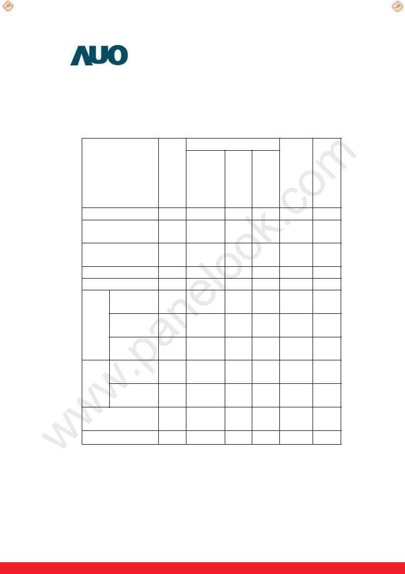
3.Measurement condition :
4. VCIM = 1.2V
VTH
VCIM
VTL
0V
5.The performance of the Lamp in LCM, for example life time or brightness, is extremely influenced by the characteristics of the DC-AC Inverter. So all the parameters of an inverter should be carefully designed so as not to produce too much leakage current from high-voltage output of the inverter. When you design or order the inverter, please make sure unwanted lighting caused by the mismatch of the lamp and the inverter (no lighting, flicker, etc) never occurs. When you confirm it, the LCD Assembly should be operated in the same condition as installed in your instrument.
6.Do not attach a conducting tape to lamp connecting wire. If the lamp wire attach to conducting tape, TFT-LCD Module have a low luminance and the inverter has abnormal action because leakage current occurs between lamp wire and conducting tape.
7.The relative humidity must not exceed 80% non-condensing at temperatures of 40 or less. At temperatures greater than 40 , the wet bulb temperature must not exceed 39 . When operate at low
 temperatures, the brightness of CCFL will drop and the life time of CCFL will be reduced.
©Copyright AU Optronics, Inc. |
|
|
January, 2003 All Rights Reserved. |
T315XW02 V2 - Specs. ver 0.6 |
9/31 |
No Reproduction and Redistribution Allowed |
|
|
One step solution for LCD / PDP / OLED panel application: Datasheet, inventory and accessory! www.panelook.com

Global LCD Panel Exchange Center |
www.panelook.com |
3-2 Interface Connections
-LCD connector (CN3): JAE FI-E30S or equivalent
Pin No |
Symbol |
Description |
note |
|
|
|
|
1 |
Reserved |
Open or High |
Auo internal test pin |
|
|
|
|
2 |
Reserved |
Open or High |
Auo internal test pin |
|
|
|
|
3 |
Reserved |
Open or High |
Auo internal test pin |
|
|
|
|
4 |
GND |
Ground and Signal Return |
|
|
|
|
|
5 |
RIN0- |
LVDS Channel 0 negative |
|
|
|
|
|
6 |
RIN0+ |
LVDS Channel 0 positive |
|
|
|
|
|
7 |
GND |
Ground and Signal Return for LVDS |
|
|
|
|
|
8 |
RIN1- |
LVDS Channel 1 negative |
|
|
|
|
|
9 |
RIN1+ |
LVDS Channel 1 positive |
|
|
|
|
|
10 |
GND |
Ground and Signal Return for LVDS |
|
|
|
|
|
11 |
RIN2- |
LVDS Channel 2 negative |
|
|
|
|
|
12 |
RIN2+ |
LVDS Channel 2 positive |
|
|
|
|
|
13 |
GND |
Ground and Signal Return for LVDS |
|
|
|
|
|
14 |
RCLK- |
LVDS Clock negative |
|
|
|
|
|
15 |
RCLK+ |
LVDS Clock positive |
|
|
|
|
|
16 |
GND |
Ground and Signal Return for LVDS |
|
|
|
|
|
17 |
RIN3- |
LVDS Channel 3 negative |
|
|
|
|
|
18 |
RIN3+ |
LVDS Channel 3 positive |
|
|
|
|
|
19 |
GND |
Ground and Signal Return |
|
|
|
|
|
20 |
Reserved |
Open or High |
AUO internal test pin |
|
|
|
|
21 |
LVDS Option |
Low for JEIDA, High/Open for NS |
|
|
|
|
|
22 |
Rotate |
High: U/D, R/L rotate, L (GND)/Open: Normal |
|
|
|
|
|
23 |
GND |
Ground and Signal Return |
|
|
|
|
|
24 |
GND |
Ground and Signal Return |
|
|
|
|
|
25 |
GND |
Ground and Signal Return |
|
|
|
|
|
26 |
Vcc |
5V, DC, Regulated |
|
|
|
|
|
27 |
Vcc |
5V, DC, Regulated |
|
|
|
|
|
28 |
Vcc |
5V, DC, Regulated |
|
|
|
|
|
29 |
Vcc |
5V, DC, Regulated |
|
|
|
|
|
30 |
Vcc |
5V, DC, Regulated |
|
|
|
|
|
Note:
1.All GND (ground) pins should be connected together and should also be connected to the LCD’s metal frame. All Vcc (power input) pins should be connected together.
©Copyright AU Optronics, Inc. |
|
|
January, 2003 All Rights Reserved. |
T315XW02 V2 - Specs. ver 0.6 |
10/31 |
No Reproduction and Redistribution Allowed |
|
|
One step solution for LCD / PDP / OLED panel application: Datasheet, inventory and accessory! www.panelook.com
 Loading...