


BDTIC www.BDTIC.com/ATMEL
Features
• 80C52 Compatible
• 8051 pin and instruction compatible
• Four 8-bit I/O ports
• Thr ee 16 -bit ti m e r/coun ters
• 256 bytes scratchpad RAM
• High-Speed Architecture
• 40 MHz @ 5V, 30MHz @ 3V
• X2 Speed Improvement capability (6 clocks/ m achine cycle)
– 30 MHz @ 5V, 20 MHz @ 3V (Equivalent to
– 60 MHz @ 5V, 40 MHz @ 3V)
• Dual Data Pointer
• On-chip ROM/EPROM (16K-bytes, 32K-bytes)
• Programmable Clock Out and Up/Down Timer/Counter 2
• Hardware Watchdog Timer (One-time enabled with Reset-Out)
• Asynchronous port reset
• Interrupt Structure with
• 6 Interrupt sources
• 4 level priority interrupt system
• Full duplex Enhanced UART
• Framing error detection
• Automatic address recognition
• Low EMI (inhibit ALE)
• Power Control modes
• Idle mode
• Power-down mode
• Power-off Flag
• Once mode (On-chip Emulation)
• Power supply: 4.5-5.5V, 2.7-5.5V
• Temperature ranges: Commercial (0 to 70
• Packages: PDIL40, PLCC44, VQFP44 1.4, PQFP44 F1, CQPJ4 4 (window), CDIL40
(window)
o
C) and Industrial (-40 to 85oC)
8-bit CMOS
Microcontroller
16/32 Kbytes
ROM/OTP
TS80C54/58X2
TS87C54/58X2
AT80C54/58X2
AT87C54/58X2
1. Description
TS80C54/58X2 is high perf ormance CMOS ROM , OTP an d EPROM ve rsions of the
80C51 CMOS single chip 8-bit microcontroller.
The TS80C54/58X2 retains all features of the Atmel 80C51 with extended
ROM/EPROM capacity (16/32 Kbytes), 256 bytes of internal RAM, a 6-source , 4-level
interrupt system, an on-chip oscilator and three timer/counters.
In addition , the TS 80C54 /58X2 a Ha rdware W atchd og Ti mer, a m ore ver satil e seria l
channel that facilitates multiprocessor communication ( EUART) and a X2 speed
improvement mechanism.
The fully static design of the TS80C54/58X2 allows to reduce system power consumption by bringing the clock frequency down to any value, even DC, without loss of data.
Rev. 4431E–8051–04/06
The TS80C54/58X2 has 2 software-selectable m odes of redu ce d act ivity for further reduc tion i n
power consumption. In the idle mode the CPU is frozen while the timers, the serial port and the
interrupt system are still operating. In the power-down mode the RAM is saved and all other
functions are inoperative.
PDIL40
PLCC44
PQFP44 F1
VQFP44 1.4 ROM (bytes) EPROM (bytes)
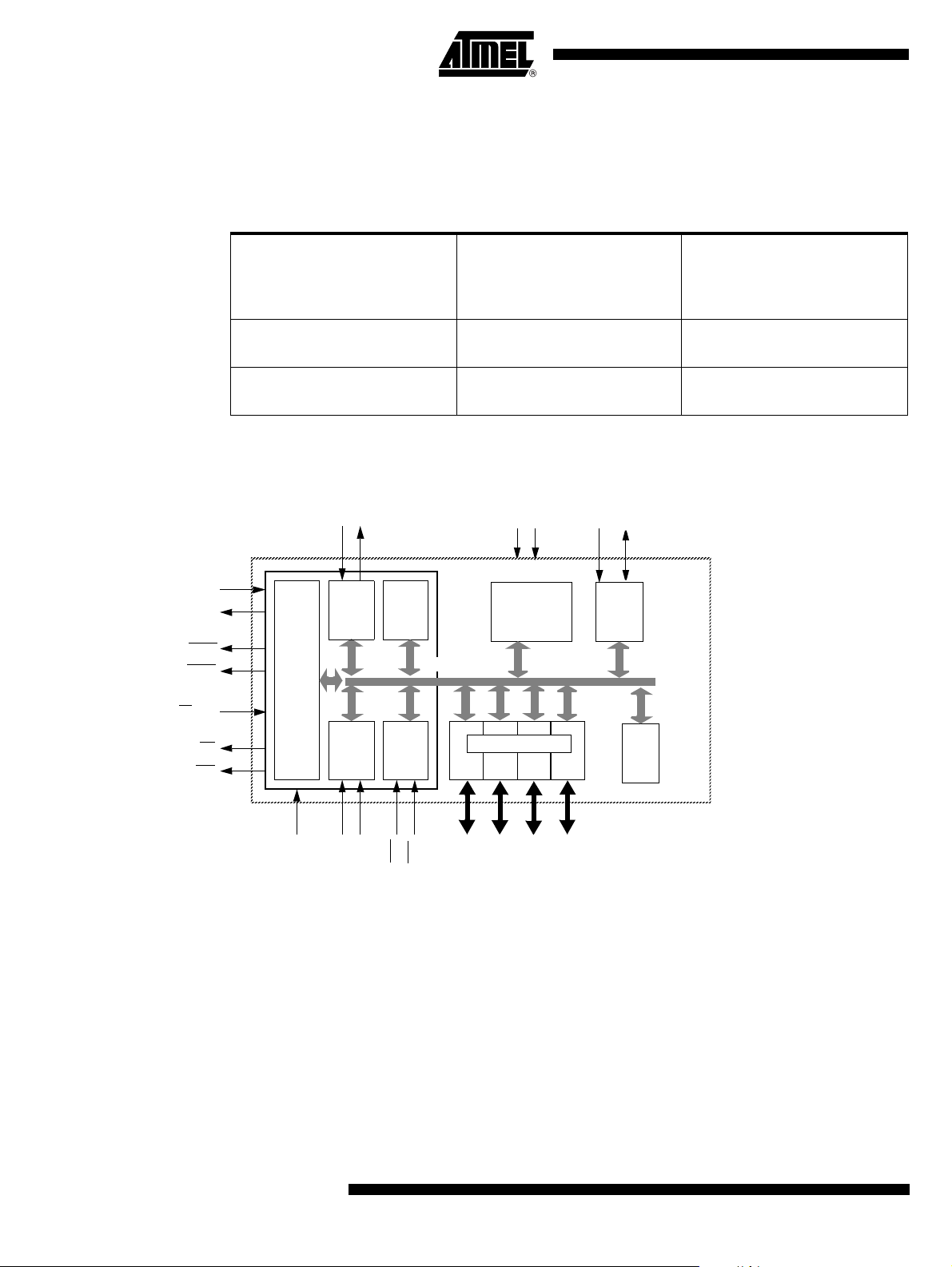
2. Block Diagram
XTAL1
XTAL2
ALE/
PROG
PSEN
EA/VPP
RD
WR
(2)
(2)
TS80C54X2
TS80C58X2
TS87C54X2
TS87C58X2
CPU
RxD
(2)(2)
EUART
Timer 0
Timer 1
TxD
C51
CORE
RAM
256x8
INT
Ctrl
IB-bus
Parallel I/O Ports
Port 0
Port 1
Vss
Vcc
ROM
/EPROM
16/32Kx8
Port 2
16k
32k
0
0
Port 3
T2EX
(1) (1)
Timer2
T2
Watch
Dog
0
0
16k
32k
(2) (2) (2) (2)
P1
P2
T0
T1
RESET
2
AT/TS8xC54/8X2
INT1
INT0
(1): Alternate function of Port 1
(2): Alternate function of Port 3
P0
P3
4431E–8051–04/06

4. SFR Mapp in g
AT/TS8xC54/8X2
The Special Function Registers (SFRs) of the TS80C54/58X2 fall into the following categories:
• C51 core registers: ACC, B, DPH, DPL, PSW, SP, AUXR1
• I/O port regi s ters: P0, P1, P2, P3
• Timer registers: T2CON, T2MOD, TCON, TH0, TH1, TH2, TMOD, TL0, TL1, TL2, RCAP2L,
RCAP2H
• Serial I/O port registers: SADDR, SADEN, SBUF, SCON
• Power and clock control registers: PCON
• HDW Watchdog Timer Reset: WDTRST, WDTPRG
• Inter r u p t syste m regi s te r s: IE , IP, IPH
• Oth ers: AUXR, CKCON
4431E–8051–04/06
3

Table 4-1. All SFRs with their address and their reset value
Bit
Non Bit addressable
address-
able
0/8 1/9 2/A 3/B 4/C 5/D 6/E 7/F
F8h FFh
F0h
E8h EFh
E0h
D8h DFh
D0h PSW
C8h
C0h
B8h
B0h
A8h
A0h
98h
90h
88h
80h
B
0000 0000
ACC
0000 0000
0000 0000
T2CON
0000 0000
IP
XX00 0000
P3
1111 1111
IE
0X00 0000
P2
1111 1111
SCON
0000 0000
P1
1111 1111
TCON
0000 0000
P0
1111 1111
T2MOD
XXXX XX00
SADEN
0000 0000
SADDR
0000 0000
SBUF
XXXX XXXX
TMOD
0000 0000
SP
0000 0111
RCAP2L
0000 0000
AUXR1
XXXX 0XX0
TL0
0000 0000
DPL
0000 0000
RCAP2H
0000 0000
TL1
0000 0000
DPH
0000 0000
TL2
0000 0000
TH0
0000 0000
TH2
0000 0000
TH1
0000 0000
WDTRST
XXXX XXXX
AUXR
XXXX XXX0
IPH
XX00 0000
WDTPRG
XXXX X000
CKCON
XXXX XXX0
PCON
00X1 0000
F7h
E7h
D7h
CFh
C7h
BFh
B7h
AFh
A7h
9Fh
97h
8Fh
87h
0/8 1/9 2/A 3/B 4/C 5/D 6/E 7/F
reserved
4
AT/TS8xC54/8X2
4431E–8051–04/06
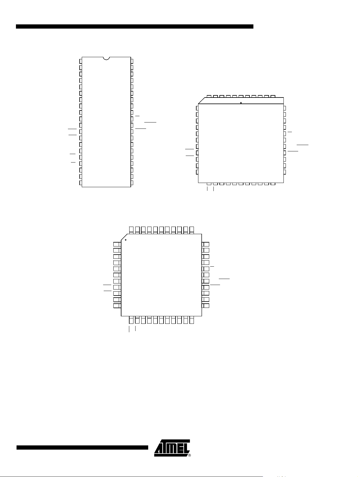
5. Pin Configurat ion
G
AT/TS8xC54/8X2
P1.0 / T2
P1.1 / T2EX
P1.2
P1.3
P1.4
P1.5
P1.6
P1.7
RST
P3.0/RxD
P3.1/TxD
P3.2/INT0
P3.3/INT1
P3.4/T0
P3.5/T1
P3.6/WR
P3.7/RD
XTAL2
XTAL1
VSS
1
2
3
4
5
6
7
8
9
10
11
12
13
14
15
16
17
18
19
20
PDIL/
CDIL40
40
39
38
37
36
35
34
33
32
31
30
29
28
27
26
25
24
23
22
21
VCC
P0.0 / A0
P0.1 / A1
P0.2 / A2
P0.3 / A3
P0.4 / A4
P0.5 / A5
P0.6 / A6
P0.7 / A7
EA/VPP
ALE/PROG
PSEN
P2.7 / A15
P2.6 / A14
P2.5 / A13
P2.4 / A12
P2.3 / A11
P2.2 / A10
P2.1 / A9
P2.0 / A8
P1.4
P1.3
P1.2
P0.1/AD1
P0.2/AD2
P0.3/AD3
39
38
37
36
35
34
33
32
31
30
29
P0.4/AD4
P0.5/AD5
P0.6/AD6
P0.7/AD7
EA/VPP
NIC*
ALE/PRO
PSEN
P2.7/A15
P2.6/A14
P2.5/A13
P1.5
P1.6
P1.7
RST
P3.0/RxD
NIC*
P3.1/TxD
P3.2/INT0
P3.3/INT1
P3.4/T0
P3.5/T1
7
8
9
10
11
12
13
14
15
16
17
P1.4
P1.3
5 4 3 2 1 6
P1.0/T2
P1.1/T2EX
P1.2
PLCC/CQPJ 44
VSS1/NIC*
VCC
P0.0/AD0
44 43 42 41 40
18 19 20 21 22 2 3 24 25 26 27 28
NIC*
VSS
XTAL2
XTAL1
P3.7/RD
P3.6/WR
P1.0/T2
P1.1/T2EX
VSS1/NIC*
VCC
P0.0/AD0
P0.2/AD2
P0.3/AD3
P0.1/AD1
P2.0/A8
P2.1/A9
P2.2/A10
P2.3/A11
P2.4/A12
P3.0/RxD
P3.1/TxD
P3.2/INT0
P3.3/INT1
*NIC: No Internal Connection
P1.5
P1.6
P1.7
RST
NIC*
P3.4/T0
P3.5/T1
43 42 41 40 3944 38 37 36 35 34
1
2
3
4
5
6
7
8
9
10
11
PQFP44 F1
VQFP44 1.4
12 13 14 15 16 17 18 19 20 21 22
VSS
NIC*
XTAL1
P3.6/WR
P3.7/RD
XTAL2
P2.0/A8
P2.1/A9
P0.4/AD4
33
32
P0.5/AD5
31
P0.6/AD6
30
P0.7/AD7
29
EA/VPP
28
NIC*
27
ALE/PROG
26
PSEN
25
P2.7/A15
24
P2.6/A14
23
P2.5/A13
P2.3/A11
P2.2/A10
P2.4/A12
4431E–8051–04/06
5
Table 5-1. Pin Description for 40/44 pin packages
PIN NUMBER
MNEMONIC
V
SS
Vss1 1 39 I Optional Ground: Contact the Sales Office for ground connection.
V
CC
P0.0-P0.7 39-32 43-36 37-30 I/O Port 0: Port 0 i s an ope n-d r ain, bi di rec ti on al I/O p or t. P ort 0 p in s that ha ve 1s wr it ten to
P1.0-P1.7 1-8 2-9 40-44
P2.0-P2.7 21-28 24-31 18-25 I/O Port 2: Port 2 i s an 8-bit bidirectional I/O port with internal pull-ups. Port 2 pins that
P3.0-P3.7 10-17 11,
Reset 9 10 4 I Reset: A high on this pin for two machine cycles while the oscilla tor is running, resets
20 22 16 I Ground: 0V reference
40 44 38 I
1-3
12 40 I/OT2 (P1. 0): Timer/Counter 2 external count input/Clockout
23 41 IT2EX (P1.1): Timer/Counter 2 Reload/Captur e/Direct ion Control
13-19
10 11 5 I RXD (P3.0): Serial input port
11 13 7 O TXD (P3.1): Serial output port
12 14 8 I INT0
13 15 9 I INT1
14 16 10 I T0 (P3. 4): Timer 0 ext ernal inp ut
15 17 11 I T1 (P3. 5): Timer 1 external inp ut
16 18 12 O WR
17 19 13 O RD
5,
7-13
TYPE
Power Supply: This is the power supply voltage for normal, idle and power-down
operation
them floa t and can be used as hig h i mpe da nc e in put s. Por t 0 p ins must be pol ari ze d t o
Vcc or Vss in order to prevent any parasitic current consumption. Port 0 is also the
multip le xe d low-ord er addres s an d data bus durin g ac c es s to ex ternal program and
data memor y. In this ap plic at io n, i t uses st r ong i nt ern al pu ll -up wh en em it t in g 1s. Po rt 0
also i nput s t he co de by te s dur i ng E PRO M pr ogr a mmi ng. Ex ter na l pu ll -up s ar e r eq ui red
during program verification during which P0 outputs the code bytes.
I/O Port 1: Port 1 is an 8-bit bidirectional I/O port with internal pull-ups. Port 1 pins that
have 1s written t o them are pulled high by the internal pull-ups and can be used as
inputs. As inputs, Port 1 pins that are externally pulled low will source current because
of the int e rnal pu ll -up s. Por t 1 also r ec ei ve s the lo w -or der ad dres s byt e duri ng memo ry
programming and verification.
Alter nate func tions for Port 1 include:
have 1s written t o them are pulled high by the internal pull-ups and can be used as
inputs. As inputs, Port 2 pins that are externally pulled low will source current because
of the internal pull-ups. Port 2 emits the high-order address byte during fetches from
external progr am memory and during accesses to external data memor y that use 16 bit addresses (MO VX @DPTR).In this applicat ion, it uses strong internal pull-ups
emitti ng 1 s. Dur ing ac ces se s t o e xter na l data memory that u se 8- bi t ad dr es se s (MOV X
@Ri), port 2 emits the contents of the P2 SFR. Some Port 2 pins receive the high order
address bits during EPROM programming and verification:
P2.0 to P2.5 for A8 to A13
I/O Port 3: Port 3 is an 8-bit bidirectional I/O port with internal pull-ups. Port 3 pins that
have 1s written t o them are pulled high by the internal pull-ups and can be used as
inputs. As inputs, Port 3 pins that are externally pulled low will source current because
of the internal pull-ups. Some Port 3 pin P3.4 receive the high order address bits during
EPROM programming and verification for TS8xC58X2 devices.
Port 3 al so serves t he special features of the 80C51 family, as listed below.
(P3.2): External interrupt 0
(P3.3): External interrupt 1
(P3.6): External data memory write strobe
(P3.7): External data memory read strobe
P3.4 also receives A14 during TS87C58X2 EPROM Programming.
the device. An internal diffused resistor to V
externa l capacit or to V
CC.
Name And FunctionDIL LCC VQFP 1.4
permits a power-on reset using only an
SS
6
AT/TS8xC54/8X2
4431E–8051–04/06
AT/TS8xC54/8X2
Table 5-1. Pin Description for 40/44 pin packages
PIN NUMBER
MNEMONIC
MNEMONIC PIN NUMBER TYPE NAME AND FUNCTION
ALE/PROG 30 33 27 O (I) Address Latch Enable/Program Pulse: Output pulse for latching the low byte of the
PSEN 29 32 26 O Program Store ENable: The read strobe to external program memory. When
EA
/V
PP
XTAL1 19 21 15 I
31 35 29 I External Access Enable/Programming Supply Voltage: EA must be externally held
TYPE
Name And FunctionDIL LCC VQFP 1.4
address during an access to external memory. In normal operation, ALE is emitted at a
const ant rate of 1/6 (1/3 in X2 mode) the oscillator frequency, and can be used for
external timing or clocking. Note that one ALE pu lse is skipped during each access to
external data memory. This pin is also the program pulse input (PROG
programming. ALE can be disabled by setting SFR’s AUXR.0 bit. With this bit set, ALE
will be inactive during internal fetches.
executing code from the external program memory, PSEN
machine cycle, except that two PSEN
external data memory. PSEN
memory.
low to enable the device to fetch code from external program memory locations 0000H
and 3FFFH (54X2) or 7FFFH (5 8X2). If EA is held hi gh, the de vice executes from
internal progr am memory unless the pr ogram cou nter contains an address greater
than 3FFFH (54X2) or 7FFFH (58X2). This pin also receives the 12.75V programming
supply voltage (V
EA
will be internally latched on Reset.
Crystal 1: Input to the inverting oscillator amplifier and i nput to the internal clock
generator circuits.
) during EPROM programming. If security level 1 is progra mmed,
PP
is not activated duri ng fetc he s fro m inter n al prog ram
activations are skipped during each access to
is activated twice each
) during EPROM
XTAL2 18 20 14 O Crystal 2: Output from the inverting oscillator amplifier
4431E–8051–04/06
7
6. TS80C54/58X2 Enhanced Features
In comparison to t he origina l 80 C52, the T S 80C54/ 58X 2 imp lement s s om e new features, which
:
are
• The X2 option.
• The Dual Data Pointer.
• The Watchdog.
• The 4 level interrupt priority system.
• The power-off flag.
• The ONCE mod e.
• The AL E disabling.
• Som e enhanced features are also located in the UART and the timer 2.
6.1 X2 Feature
The TS80C54/58X2 core needs only 6 clock periods per machine cycle. This feature called ”X2”
provides the following advantages:
• Divide frequency crystals by 2 (cheaper crystals) while keeping same CPU power.
• Save power c onsum ption while keeping same CPU power (oscillator power saving).
• Save power c onsum ption by dividing dynam ically operating fre quency by 2 in operating and
idle modes.
• Increas e CPU power by 2 while keeping same crystal frequency.
In order to keep the original C51 compatibility, a divider by 2 is inserted between the XTAL1 signal and the main clock input of the core (phase generator). This divider may be disabled by
software.
6.1.1 Description
The clock for the whole circuit and peripheral is first divided by two before being used by the
CPU core and peripherals. This allows any cyclic ratio to be accepted on XTAL1 input. In X2
mode, as this divider is bypassed, the signals on XTAL1 must have a cyclic ratio between 40 to
60%. Figure 6-2. sho ws the clock generat ion block diag ram. X 2 bit is v al idated on XTAL1÷2 rising edge to av oid gl itc hes when sw itch ing f rom X2 to STD mod e. Fig ure 6- 2. sho ws th e mo de
switching waveforms.
Figure 6-1. Clock Generation Diagram
XTAL1:2
XTAL1
F
XTAL
2
X2
CKCON reg
0
1
F
OSC
state machine: 6 clock cycles.
CPU control
8
AT/TS8xC54/8X2
4431E–8051–04/06
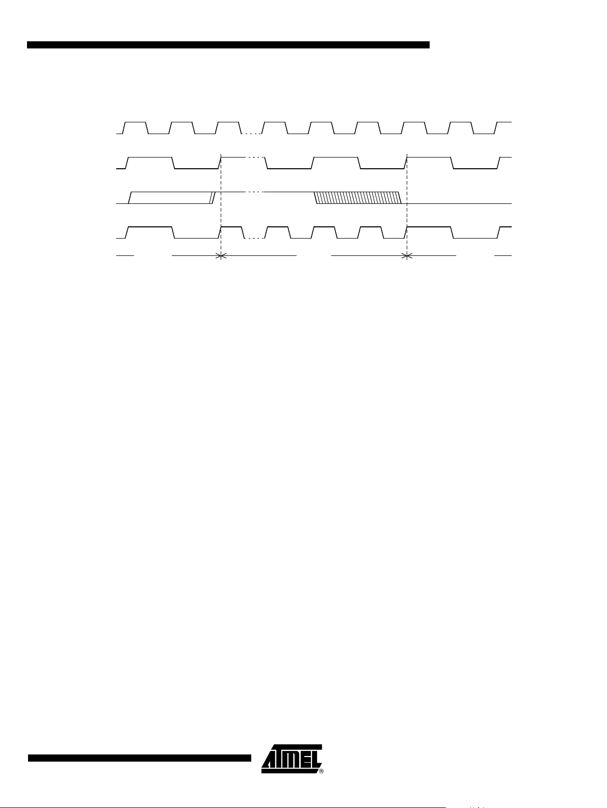
Figure 6-2. Mode Switching Waveforms
XTAL1
XTAL1:2
X2 bit
CPU clock
The X2 bit in the CKCON register (See Table 6-1.) allows to switch from 12 clock cycles per
instruction to 6 clock cycles and vice versa. At reset, the standard speed is activated (STD
mode). Setting this bit activates the X2 feature (X2 mode).
CAUTION
In order to prevent any incorrect operation while operating in X2 mode, user must be awa re that
all peripherals using clock frequency as time reference (UART, timers ) will have their time reference divided by two. Fo r exampl e a free runnin g timer gen erating an i nterrup t every 20 m s will
then generate an interrupt every 10 ms. UART with 4800 baud rate will have 9600 baud rate.
AT/TS8xC54/8X2
X2 ModeSTD Mode STD Mo de
4431E–8051–04/06
9

Table 6-1. CKCON Register
CKCON - Clock Control Register (8Fh)
76543210
-------X2
Bit
Number
7-
6-
5-
4-
3-
2-
1-
0X2
Bit
Mnemonic Description
Reserved
The value read from this bit is indeterminate. Do not set this bit.
Reserved
The value read from this bit is indeterminate. Do not set this bit.
Reserved
The value read from this bit is indeterminate. Do not set this bit.
Reserved
The value read from this bit is indeterminate. Do not set this bit.
Reserved
The value read from this bit is indeterminate. Do not set this bit.
Reserved
The value read from this bit is indeterminate. Do not set this bit.
Reserved
The value read from this bit is indeterminate. Do not set this bit.
CPU and peripheral clock bit
Clear to select 12 clock periods per machine cycle (STD mode, F
Set to sel ect 6 clock pe riods per machine cy cle (X2 mode, F
Reset Value = XXXX XXX0b
Not bit addressable
OSC=FXTAL
OSC=FXTAL
/2).
).
For further details on the X2 feature, please refer to ANM072 available on the web
(http://www.atmel.com)
10
AT/TS8xC54/8X2
4431E–8051–04/06
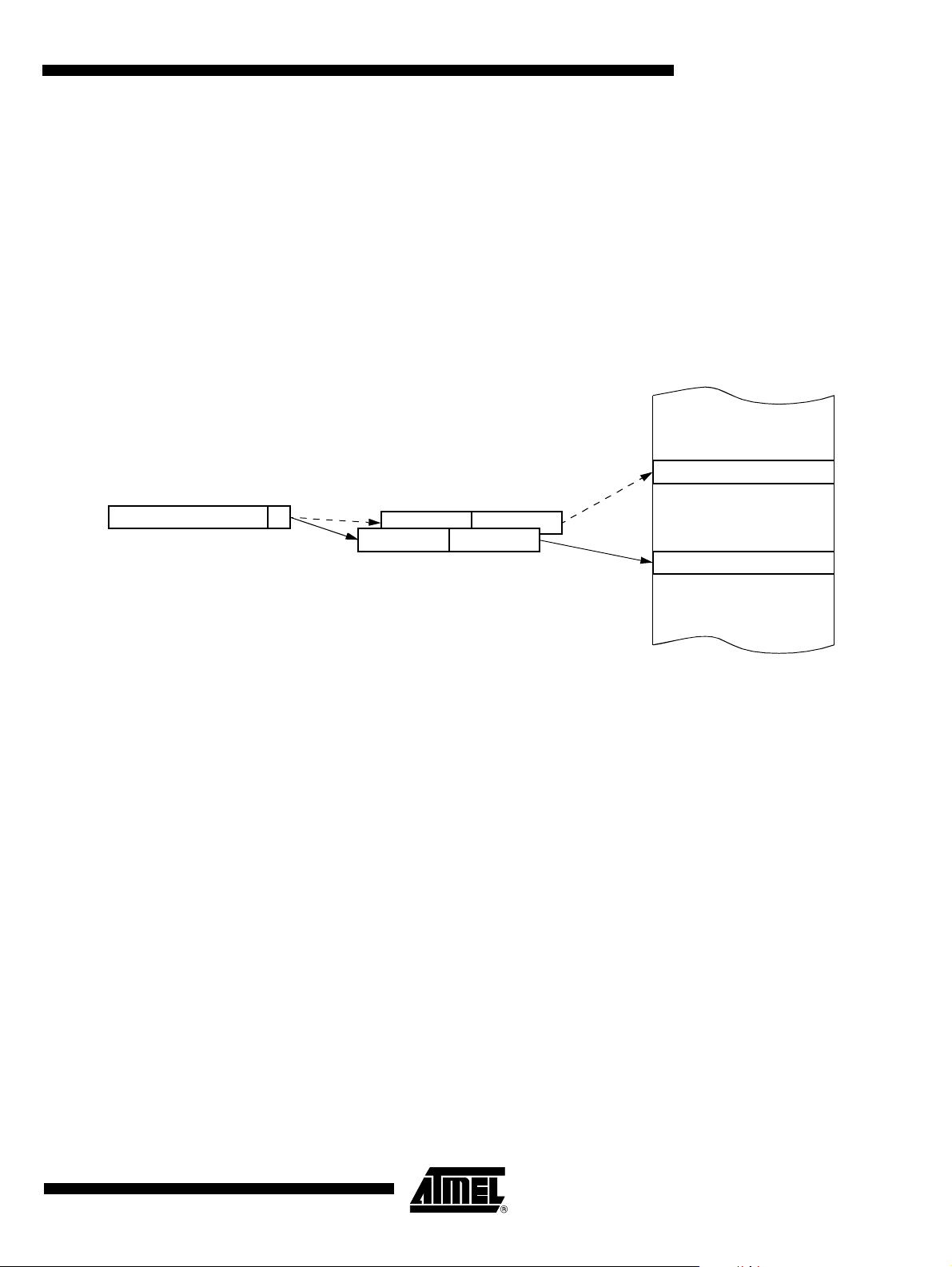
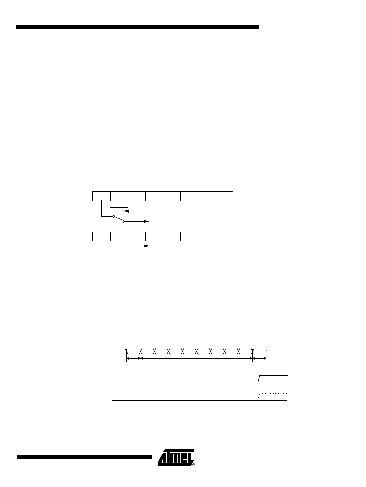
7. Dual Data Pointer Register Ddptr
The additional data pointer c an be used to spee d up code execut ion and reduce code size in a
number of ways.
The dual DPTR structure is a way by which the chip will specify the address of an external data
memory location. There are two 16-bit DP TR registers that add ress the ext ernal mem ory, an d a
single bit called
DPS = AUXR1/bit0 (See Tab le 7-1.) that allows the program code to s witch between them
(Refer to Figure 7-1).
Figure 7-1. Use of Dual Pointer
07
DPS
AUXR1(A2H)
DPH(83H) DPL(82H)
DPTR1
AT/TS8xC54/8X2
External Data Memory
DPTR0
4431E–8051–04/06
11

Table 7-1. AUXR1: Auxiliary R e gister 1
76543210
----GF30-DPS
Bit
Number
7-
6-
5-
4-
3 GF3 This bit is a general purpose user flag
20
1-
0DPS
Bit
Mnemonic Description
Reserved
The value read from this bit is indeterminate. Do not set this bit.
Reserved
The value read from this bit is indeterminate. Do not set this bit.
Reserved
The value read from this bit is indeterminate. Do not set this bit.
Reserved
The value read from this bit is indeterminate. Do not set this bit.
Reserved
Always st uck at 0.
Reserved
The value read from this bit is indeterminate. Do not set this bit.
Data Pointer Selection
Clear to select DPTR0.
Set to selec t DPTR1 .
Reset Value = XXXX 00X0
Not bit addressable
User software should not write 1s to reserved bits. These bits may be used in future 8051 family
products to invoke new feature. In that case, the reset value of the new bit will be 0, and its
active value will be 1. The value read from a reserved bit is indeterminate.
12
AT/TS8xC54/8X2
4431E–8051–04/06

7.1 Application
AT/TS8xC54/8X2
Software can take advantage of the additional data pointers to both increase speed and reduce
code size, for e xample , block o perations (copy, co mpare, se arch ...) are we ll served by using
one data pointer as a ’source’ pointer and the other one as a "destination" pointer.
ASSEMBLY LANGUAG E
; Block move using dual data pointers
; Destroys DPTR0, DPTR1, A and PSW
; note: DPS exits opposite of entry state
; unless an extra INC AUXR1 is added
;
00A2 AUXR1 EQU 0A2H
;
0000 909000 MO V DPTR,#SOURCE ; address of SOURCE
0003 05A2 INC AUXR1 ; switch data pointers
0005 90A000 MOV DPTR,#DEST ; address of DEST
0008 LOOP:
0008 05A2 INC AUXR1 ; switch data pointers
000A E0 MOVX A,@DPTR ; get a byte from SOURCE
000B A3 INC DPTR ; increment SOURCE address
000C 05A2 INC AUXR1 ; switch data pointers
000E F0 MOVX @DP TR,A ; write the byte to DEST
000F A 3 INC DPTR ; increment DEST address
0010 70F6 JNZ LOOP ; check for 0 terminator
0012 05A2 INC AUXR1 ; (optional) restore DPS
INC is a short (2 bytes) and fast (12 clocks) way to manipulate the DPS bit in the AUXR1 SFR.
However, no te that the I NC instruct ion d oes not di rectl y force th e DPS b it to a p articula r state,
but simply toggles it. In simple routines, such as the block move example, only the fact that DPS
is toggled in the pro per s equence mat ters, not i ts act ual val ue. In oth er words , the b lock mo ve
routine works the same whether DPS is '0' or '1' on entry. Observ e that without the last instruction (INC AUXR1), the routine will exit with DPS in the opposite state.
4431E–8051–04/06
13

8. Timer 2
The timer 2 in the TS80C54/58X2 is compatible with the timer 2 in the 80C52.
It is a 16-bit timer/counter: the count is maintained by two eight-bit timer registers, TH2 and TL2,
connected in cascad e. It is cont rolled by T2CON reg ister (See Table 8-1) an d T2M OD regi ster
(See Table 8-2). Timer 2 operation is similar to Timer 0 and Timer 1. C/T2
operation) or external pin T2 (counter operation) as the timer clock input. Setting TR2 allows TL2
to be incremented by the selected input.
Timer 2 has 3 o pe rating mode s: cap ture , au tore load a nd Bau d R ate G ener ator . Thes e m odes
are selected by the combination of RCLK, TCLK and CP/RL2
Atmel Wireless & Microcontrollers 8-bit Microcontroller Hardware description.
Refer to the Atmel Wireless & Microcontrollers 8-bit Microcontroller Hardware description for the
description of Capture and Baud Rate Generator Modes.
TS80C54/58X2 Timer 2 includes the following enhancements:
In
• Aut o-reload mode with up or down counter
• Program m able clock- output
8.1 Auto-Reload Mode
The auto-reload mode configures timer 2 as a 16-bit timer or ev ent counter with automatic
reload. If DCEN bit in T 2M OD i s c leared, timer 2 behaves as in 80C5 2 (ref er to the Atmel Wireless & Microcontrollers 8-bit Microcontroller Hardware description). If DCEN bit is set, timer 2
acts as an Up/down timer/counter as shown in Figure 8-1. In this mode the T2EX pin controls
the direction of count.
selects F
(T2CON), as described in the
/12 (timer
OSC
When T2EX is high , timer 2 counts up. Timer overflow occurs at FFFFh which sets the TF2 flag
and genera tes an interrupt request . The overf low also cau ses the 16 -bit value in RCAP2H an d
RCAP2L registers to be loaded into the timer registers TH2 and TL2.
When T2EX is low, timer 2 counts down. Timer underflow occurs when the count in the timer
registers TH2 an d TL2 eq uals th e value st ored in RCAP2 H and RCAP2L re gisters. The un derflow sets TF2 flag and reloads FFFFh into the timer registers.
The EXF2 bit toggl es when timer 2 overflows or unde rflows acco rding to the th e di rection of t he
count. EXF2 does not generate any interrupt. This bit can be used to provide 17-bit resolution
14
AT/TS8xC54/8X2
4431E–8051–04/06
Figure 8-1. Auto-Reload Mode Up/Down Counter (DCEN = 1)
(:6 in X2 mode )
XTAL1
F
XTAL
F
OSC
:12
T2
0
1
C/T2
T2CONreg
AT/TS8xC54/8X2
TR2
T2CONreg
8.1.1 Programmable Clock-Output
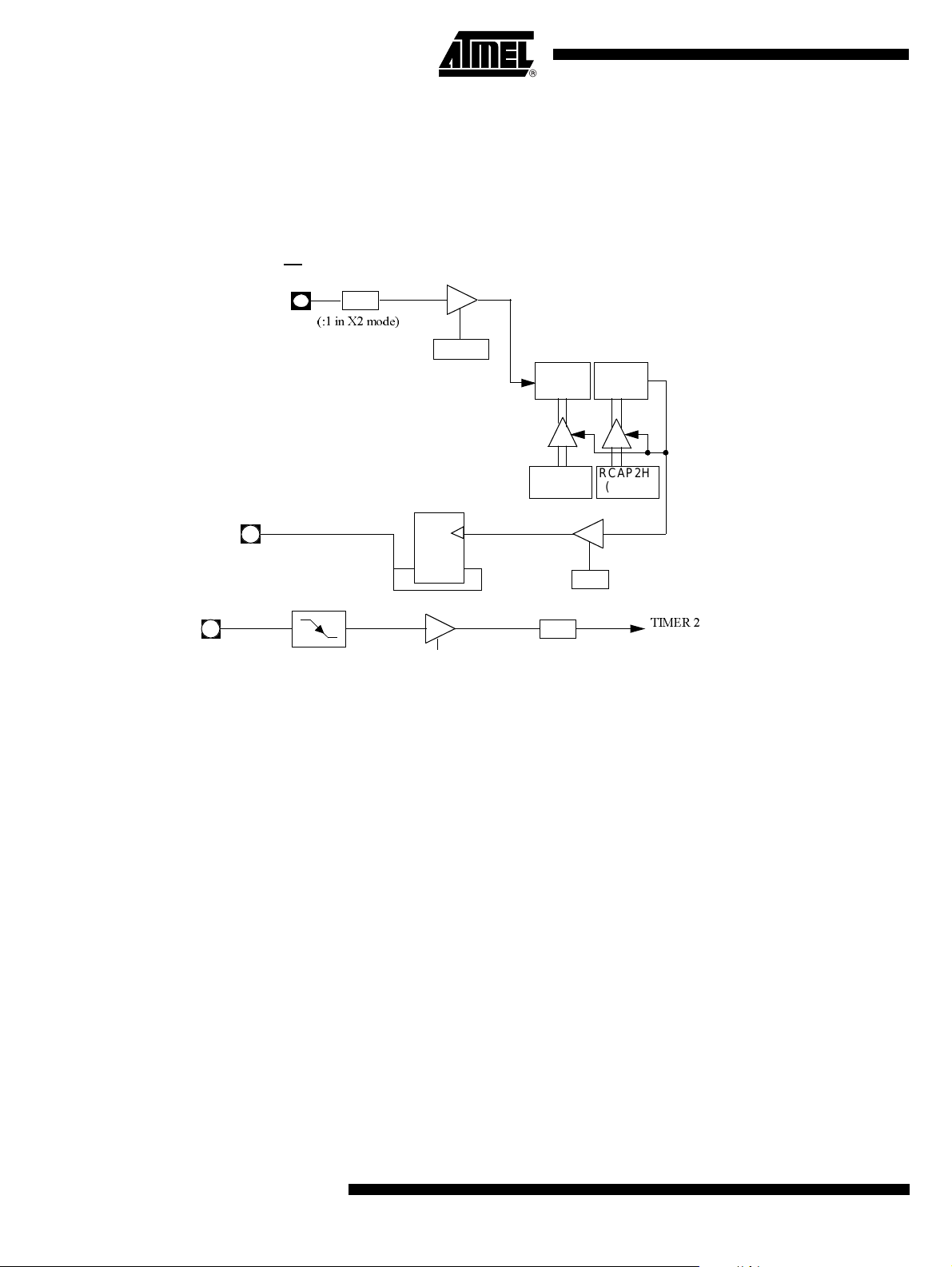
In the clock-out mode, timer 2 operates as a 50%-duty-cycle, programmable clock generator
(See Figure 8-2) . The input clock increments TL2 at frequency F
counts to overflow from a loaded value. At overflow, the contents of RCAP2H and RCA P 2L registers are load ed into TH 2 and TL2. In this mode , timer 2 overf lows do n ot gen erate int errupts.
The formula gives the clock-out frequen cy as a function of the system osci llator frequ ency and
the value in the RCAP2H and RCAP2L registers :
(DOWN COUNTING RELOAD VALUE)
FFh
(8-bit)
TL2
(8-bit)
RCAP2L
(8-bit)
(UP COUNTING RELOAD VALUE)
FFh
(8-bit)
TH2
(8-bit)
RCAP2H
(8-bit)
T2EX:
if DCEN=1, 1=UP
if DCEN=1, 0=DOWN
TOG-
TF2
T2CONreg
OSC
T2CONreg
EXF2
TIMER 2
INTERRUPT
/2. The timer repeatedly
4431E–8051–04/06
F
Cloc k OutF re quen cy
–
---------------------------------------------------------------------------------------- -=
4 65536
osc
RCAP2H–RCA P2L
⁄()×
For a 16 MHz system clock, timer 2 has a programmable frequency range of 61 Hz
(F
OSC
to 4 MHz (F
/4). The generated clock signal is brought out to T2 pin (P1.0).
OSC
16)
/2
Timer 2 is programmed for the clock-out mode as follows:
• Set T2OE bit in T2MOD register.
• Clear C/T2
bit in T2CON register.
• Determine the 16-bit reload value from the formula and enter it in RCAP2H/RCAP2L
registers.
15
• Enter a 16-bit initial value in timer registers TH2/TL2. It can be the same as the reload value
or a different one depending on the application.
• To start the timer, set TR2 run control bit in T2CON register.
It is possible to use timer 2 as a baud rate generator and a clock generator simultaneously. For
this configuration, the baud rates and clock frequencies are not independent since both functions use the values in the RCAP2H and RCAP2L registers.
Figure 8-2. Clock-Out Mode C/T2
XTAL1
T2
T2EX
= 0
:2
(:1 in X2 mode)
TR2
T2CON reg
Toggle
QD
EXEN2
T2CON reg
TL2
(8-bit)
RCAP2L
(8-bit)
T2OE
T2MOD reg
EXF2
T2CON reg
TH2
(8-bit)
RCAP2H
(8-bit)
OVERFLOW
TIMER 2
INTERRUPT
16
AT/TS8xC54/8X2
4431E–8051–04/06

AT/TS8xC54/8X2
Table 8-1. T2CON Register
T2CON - Timer 2 Control Register (C8h)
7 6 5 4 3 2 1 0
TF2 EXF2 RCLK TCLK EXEN2 TR2 C/T2# CP/RL2#
Bit
Number
7TF2
6 EXF2
5 RCLK
4TCLK
3 EXEN2
2TR2
1C/T2#
0CP/RL2#
Bit
Mnemonic Description
Timer 2 overflow Flag
Must be cleared by software.
Set by hardware on timer 2 overflow, if RCLK = 0 and T CLK = 0.
Timer 2 External Flag
Set when a capture or a reload is caused by a negative transition on T2EX pin if EXEN2=1.
When set, causes the CPU to vector to timer 2 interrupt routine when timer 2 interrupt is
enabled.
Must be cleared by software . EXF2 doesn’t cause an interrupt in Up/down counter mode
(DCEN = 1)
Receive Clock bit
Clear to use timer 1 overflow as receive cl ock for serial port in mode 1 or 3.
Set to use timer 2 overflow as receive clock for serial port in mode 1 or 3.
Transmit Clock bit
Clear to use timer 1 overflow as transmit clock for serial por t in mode 1 or 3.
Set to use timer 2 overflow as transm it clock fo r serial port in mode 1 or 3.
Timer 2 External Enable bit
Clear to ignore events on T2EX pin for timer 2 operation.
Set to cause a capture or rel oad when a negative transition on T2EX pin is detected, if timer
2 is not used to clock the serial port.
Timer 2 Run control bit
Clear to tu rn off timer 2.
Set to turn on timer 2.
Timer/Counter 2 select bit
Clear for timer operation (input from internal clock system: F
Set for counter oper ation (input from T2 in put pin, falling edge trigger). Must be 0 for clock
out mode.
Timer 2 Capture/Reload bit
If RCLK=1 or TCLK=1, C P/RL2# is ignored and timer is forced to auto -reload on timer 2
overflow.
Clear to auto-reload on timer 2 overflows or negative transitions on T2EX pin if EXEN2=1.
Set to capture on negative transitions on T2EX pin if EXEN2=1.
OSC
).
4431E–8051–04/06
Reset Value = 0000 0000b
Bit addressable
17

Table 8-2. T2MOD Register
T2MOD - Timer 2 Mode Control Register (C9h)
7 6 5 4 3 2 1 0
- - - - - - T2OE DCEN
Bit
Number
7-
6-
5-
4-
3-
2-
1T2OE
0 DCEN
Bit
Mnemonic Description
Reserved
The value read from this bit is indeterminate. Do not set this bit.
Reserved
The value read from this bit is indeterminate. Do not set this bit.
Reserved
The value read from this bit is indeterminate. Do not set this bit.
Reserved
The value read from this bit is indeterminate. Do not set this bit.
Reserved
The value read from this bit is indeterminate. Do not set this bit.
Reserved
The value read from this bit is indeterminate. Do not set this bit.
Timer 2 Output Enable bit
Clear to program P1.0/T2 as clock in put or I/O port.
Set to program P1.0/T2 as clock output.
Down Counter Enable bit
Clear to disabl e timer 2 as up/down counter .
Set to enable timer 2 as up/down count er.
Reset Value = XXXX XX00b
Not bit addressable
18
AT/TS8xC54/8X2
4431E–8051–04/06
9. TS80C54/58X 2 Serial I/O P ort
The serial I/O port in the TS80C54/58X2 is compatible with the serial I/O port in the 80C52.
It provides b oth synch rono us and asy nchrono us com mun ication m odes. It operate s as an Un iversal Asynchron ous Receiver an d Trans mitter (UART) i n three full-dup lex mode s (Modes 1, 2
and 3). Asynchronous transmission and reception can occur simultaneously and at different
baud rates
Serial I/O port includes the following enhancements:
• Frami ng error detection
• Aut om atic address recognition
9.1 Framing Error Detection
Framing bit error detection is provided for the three asynchronous modes (modes 1, 2 and 3). To
enable the framing bit error detection feature, set SMOD0 bit in PCON register (See Figure 9-1).
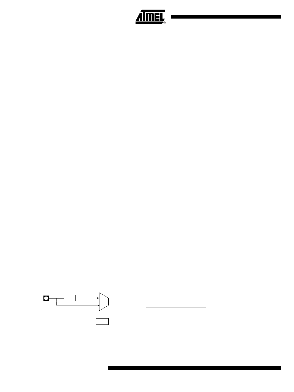
Figure 9-1. Framing Error Block Diagram
RITIRB8TB8RENSM2SM1SM0/FE
AT/TS8xC54/8X2
SCON (98h)
Set FE bit if stop bit is 0 (framing error) (SMOD0 = 1)
SM0 to UART mode control (SMOD = 0)
PCON (87h)
IDLPDGF0GF1POF-SMOD0SMOD1
To UART framing error control
When this feature is enabled, the receiver checks each incoming data frame for a valid stop bit.
An invalid stop bit may result from noise on the serial lines or from simultaneous transmission by
two CPUs. If a valid stop bit is not found, the Framing Error bit (FE) in SCON register (See Table
9-3.) bit is set.
Software may examine FE bit after each reception to check for data errors. Once set, only software or a reset c an cle ar FE bit. Subsequently received frames with valid stop bits cann ot clear
FE bit. When FE feature is enabled, RI rises on stop bit instead of the last data bit (See Figure 9-
2. and Figure 9-3.).
Figure 9-2. UART Timings in Mode 1
RXD
RI
SMOD0=X
Start
bit
Data byte
D7D6D5D4D3D2D1D0
Stop
bit
4431E–8051–04/06
FE
SMOD0=1
19

Figure 9-3. UART Timings in Modes 2 and 3
RXD
RI
SMOD0=0
RI
SMOD0=1
FE
SMOD0=1
9.1.1 Automatic Address Recognition
The automat ic addre ss recog nition f eature is en abled when the multi proce ssor comm unicat ion
feature is enabled (SM2 bit in SCON register is set).
Implemented in h ardware, aut om atic address recognition enhan ce s th e m ultiprocessor c om m unication featur e by al lowing the serial p ort to exam ine the a ddre ss of each i ncomi ng comm and
frame. O nly wh en th e seri al po rt reco gnize s its o wn ad dres s, the receive r se ts RI bi t in S CON
register to generate an interrupt. This ensures that the CPU is not interrupted by command
frames addressed to other devices.
If desired, you may enabl e t he autom ati c addres s rec ognition feature in mode 1. In this configuration, the stop bit takes the place of the ninth data bit. Bit RI is set only when the received
command frame address matches the device’s address and is terminated by a valid stop bit.
To support automatic address recognition, a device is identified by a given address and a broadcast address.
Start
bit
D8D7D6D5D4D3D2D1D0
Data byte Ninth
bit
Stop
bit
9.1.2 Given Address
20
AT/TS8xC54/8X2
NOTE: Th e mu ltiproce ssor co mm unicat ion a nd aut oma tic addr ess re cogn ition fe ature s can not
be enabled in mode 0 (i.e. setting SM2 bit in SCON register in mode 0 has no effect).
Each device has an individual address that is specified in SADDR register; the SADEN register
is a mask byte that contains don’t-care bits (defined by zeros) to form the device’s given
address. The don’t-care bits provide the flexibility to address one or more slaves at a time. The
following example illustrates how a given address is formed.
To address a device by its individual address, the SADEN mask byte must be 1111 1111b.
For example:
SADDR 0101 0110b
SADEN 1111 1100b
Given 0101 01XXb
4431E–8051–04/06

AT/TS8xC54/8X2
The following is an example of how to use given addresses to address different slaves:
Slave A: SADDR 1111 0001b
Slave B: SADDR 1111 0011b
Slave C: SADDR 1111 0010b
The SADEN byte is selected so that each slave may be addressed separately.
For slave A, bit 0 (the LSB) is a don’t-care bit; for slaves B and C, bit 0 is a 1. To communicate
with slave A only, the master must send an address where bit 0 is clear (e.g. 1111 0000b).
For slave A, bit 1 is a 1; for slaves B and C, bit 1 is a don’t care bit. To communicate with slaves
B and C, but not slave A, the master must send an address with bits 0 and 1 both set (e.g. 1111
0011b).
To communicate with slaves A, B and C, the m aster must send an ad dress with bit 0 se t, bit 1
clear, and bit 2 clear (e.g. 1111 0001b).
9.1.3 Broadcast Address
A broadcast address is formed from the logical OR of the SADDR and SADEN registers with
zeros defined as don’t-care bits, e.g.:
Broadcast =SADDR OR SADEN 1111 111Xb
SADEN 1111 1010b
Given 1111 0X0Xb
SADEN 1111 1001b
Given 1111 0XX1b
SADEN 1111 1101b
Given 1111 00X1b
SADDR 01 01 0110b
SADEN 11 11 1100b
The use of don’t-care bits provides flexibility in defining the broadcast addres s, ho wever in most
applications, a broadcast address is FFh. The following is an example of using broadcast
addresses:
Slave A: SADDR 1111 0001b
Slave B: SADDR 1111 0011b
Slave C: SADDR= 1111 0010b
For slaves A and B, bit 2 is a don’t care bi t; for slave C, bit 2 is set. To communica te with all of
the slaves, the master must send an address FFh. To communicate with slaves A and B, but not
slave C, the master can send and address FBh.
9.1.4 Reset Addresses
On reset, t he S ADDR and SA DEN registers are i nitia lized to 00h, i.e. th e given and br oad cast
addresses are XXXX XXXXb (all don’t-care bits). This ensures that the serial port will reply to any
address, and so, that it is backwards compatible with the 80C51 microcontrollers that do not
support automatic address recognition.
SADEN 1111 1010b
Broadcast 1111 1X11b,
SADEN 1111 1001b
Broadcast 1111 1X11B,
SADEN 1111 1101b
Broadcast 1111 1111b
4431E–8051–04/06
21

Table 9-1. SADEN - Slave Address Mask Register (B9h)
7 6 5 4 3 2 1 0
Reset Value = 0000 0000b
Not bit addressable
Table 9-2. SADDR - Slave Address Register (A9h)
7 6 5 4 3 2 1 0
Reset Value = 0000 0000b
Not bit addressable
22
AT/TS8xC54/8X2
4431E–8051–04/06

AT/TS8xC54/8X2
Table 9-3. SCON Register
SCON - Serial Control Register (98h)
7 6 5 4 3 2 1 0
FE/SM0 SM1 SM2 RE N TB8 RB8 TI RI
Bit
Number
7 FE
6 SM1
5 SM2
4 REN
3 TB8
2 RB8
Bit
Mnemonic
SM0
Description
Framing Error bit (SMOD0=1)
Clear to reset the error state, not c leared by a valid stop bit.
Set by hardware when an invalid stop bit is detected.
SMOD0 must be set to enable access to the FE bit
Serial port Mode bit 0
Refer to SM1 for serial port mode selection.
SMOD0 must be cleared to enable access to the SM0 bit
Serial port Mode bit 1
SM0
0 0 0 Shift RegisterF
0 1 1 8-bit UARTVariable
10 2 9-bit UARTF
1 1 3 9-bit UARTVariable
Serial port Mode 2 bit / Multipro ce ssor Comm un ica tio n Enab le bit
Clear to disable multiprocessor communication feature.
Set to enable multiprocess or communication feature in mode 2 and 3, and eventually mode
1. This bit should be cleared in mode 0.
Reception Enable bit
Clear to disable serial reception.
Set to enable seri al rec e pt i on .
Transmitter Bit 8 / Ninth bit to transmit in modes 2 and 3.
Clear to transmit a logic 0 in the 9th bit.
Set to transmit a logic 1 in the 9th bit.
Receiver Bit 8 / Ninth bit received in modes 2 and 3
Cleared by hardware if 9th bit received is a logic 0.
Set by hardware if 9th bit received is a logic 1.
In mode 1, if SM2 = 0, RB8 is the received stop bit. In mode 0 RB8 is not used.
SM1Mode Description Baud Rate
/12 (/6 in X2 mode)
XTAL
/64 or F
XTAL
/32 (/32, /16 in X2 mode)
XTAL
4431E–8051–04/06
Transmit Interrupt flag
1 TI
0 RI
Clear t o acknowl edge interrupt.
Set by hardware at the end of the 8th bit tim e in mode 0 or at the beginning of the stop bit in
the other modes.
Receive Inter rup t flag
Clear t o acknowl edge interrupt.
Set by hardware at the end of the 8th bit time in mode 0, see Figure 9-2. and Figure 9-3. in
the other modes .
Reset Value = 0000 0000b
Bit addressable
23

Table 9-4. PCON Register
Table 9-5. PCON - Power Control Register (87h)
7 6 5 4 3 2 1 0
SMOD1 SMOD0 - POF GF1 GF0 PD IDL
Bit
Number
Mnemonic
7 SMOD1
6 SMOD0
5 -
4 POF
3 GF1
2 GF0
1 PD
0 IDL
Bit
Description
Serial port Mode bit 1
Set to select double baud ra te in mode 1, 2 or 3.
Serial port Mode bit 0
Clear to select SM0 bit in SCON register.
Set to to select FE bit in SCON registe r.
Reserved
The value read from this bit is indeterminate. Do not se t this bit.
Power-Off Flag
Clear to recognize next reset type.
Set by hardware when VCC rises from 0 to its nominal voltage. Can also be set by software.
General purpose Flag
Cleared by user for general purpose usage.
Set by us er for general purpose usage.
General purpose Flag
Cleared by user for general purpose usage.
Set by us er for general purpose usage.
Power-Down mode bit
Cleared by hardware when reset occurs.
Set to ent er pow er-down mo de.
Idle mode bit
Clear by hardware when interrupt or reset occurs.
Set to enter idle mode.
24
Reset Value = 00X1 0000b
Not bit addressable
Power-off flag reset value will be 1 only after a power on (cold reset). A warm reset doesn’t affect
the value of this bit.
AT/TS8xC54/8X2
4431E–8051–04/06

10. Inter r upt S yst em
High priority
The TS80C54/58X2 has a total of 7 interrupt vectors: two external interrupts (INT0 and INT1),
three timer interrupts (timers 0, 1 and 2) and the serial port interrupt. These interrupts are shown
in Figure 10-1.
Figure 10-1. I nt errupt Control System
AT/TS8xC54/8X2
INT0
TF0
INT1
TF1
RI
TF2
EXF2
IPH, IP
IE0
IE1
TI
3
0
3
0
3
0
3
0
3
0
3
0
Global D is ab leIndividual Enable
interrupt
Interrupt
polling
sequence, decreasing from
high to low priority
Low priority
interrupt
4431E–8051–04/06
Each of the interrupt sources can be individually enabled or disabled by setting or clearing a bit
in the Interrupt Enable register (See Table 10-2.). This register also contains a global disable bit,
which must be cleared to disable all interrupts at once.
Each inte rrup t sour ce ca n also be ind ividu ally p rogram me d to o ne out o f fo ur pri ority lev els by
setting or clearing a bit in the Interrupt Priority register (See Table 10-3.) and in the Interrupt Priority High register (See Table 10-4.). shows the bit values and priority levels associated with
each combination.
Table 10-1. Priority Leve l Bi t V alu es
IPH.x IP.x Interrupt Le ve l Prior ity
0 0 0 (Lowest)
011
102
1 1 3 (Highest)
A low-priority interrupt can be interrupted by a high priority i nterrupt, but not by another low-priority interrupt. A high-priority interrupt can’t be interrupted by any other interrupt source.
25

If two interrupt requests of different priority levels are received simultaneously, the request of
higher priority level is serviced. If interrupt requests of the same priority level are received simultaneously, an internal polling sequence determines which request is serviced. Thus within each
priority level there is a second priority structure determined by the polling sequence.
Table 10-2. IE Regist e r
IE - Interrupt Enable Register (A8h)
7 6 5 4 3 2 1 0
EA - ET2 ES ET1 EX1 ET0 EX0
Bit
Number
7 EA
6 -
5 ET2
4 ES
3 ET1
2 EX1
1 ET0
0 EX0
Bit
Mnemonic Description
Enable All interrupt bit
Clear to disable all interrupts.
Set to enable all int err u pts .
If EA=1, each interrupt source is individually enabled or disabled by setting or clearing its
own interrupt enable bit.
Reserved
The value read from this bit is indeterminate. Do not set this bit.
Timer 2 overflow interr upt Enable bit
Clear t o disable timer 2 overflow in terrupt.
Set to enable timer 2 overflow interrupt.
Serial por t Enable bi t
Clear to disable serial port interrupt.
Set to enable seri al po rt int err u pt .
Timer 1 overflow interr upt Enable bit
Clear t o disable timer 1 overflow in terrupt.
Set to enable timer 1 overflow interrupt.
External interrupt 1 Enable bit
Clear to disable external interrupt 1.
Set to enable exte rna l in terr up t 1.
Timer 0 overflow interr upt Enable bit
Clear t o disable timer 0 overflow in terrupt.
Set to enable timer 0 overflow interrupt.
External interrupt 0 Enable bit
Clear to disable external interrupt 0.
Set to enable exte rna l in terr up t 0.
26
Reset Value = 0X00 0000b
Bit addressable
AT/TS8xC54/8X2
4431E–8051–04/06

AT/TS8xC54/8X2
Table 10-3. IP Regist e r
IP - Interrupt Priority Register (B8h)
7 6 5 4 3 2 1 0
- - PT2 PS PT1 PX1 PT0 PX0
Bit
Number
7 -
6 -
5 PT2
4 PS
3 PT1
2 PX1
1 PT0
0 PX0
Bit
Mnemonic Description
Reserved
The value read from this bit is indeterminate. Do not set this bit.
Reserved
The value read from this bit is indeterminate. Do not set this bit.
Timer 2 overflow interrupt Priority bit
Refer to PT2H for priority level.
Serial port Priority bit
Refer to PSH for priority level.
Timer 1 overflow interrupt Priority bit
Refer to PT1H for priority level.
External interrupt 1 Priority bit
Refer to PX1H for priority level.
Timer 0 overflow interrupt Priority bit
Refer to PT0H for priority level.
External interrupt 0 Priority bit
Refer to PX0H for priority level.
Reset Value = XX00 0000b
Bit addressable
4431E–8051–04/06
27

Table 10-4. IPH Register
IPH - Interrupt Priority High Register (B7h)
7 6 5 4 3 2 1 0
- - PT2H PSH PT1H PX1H PT0H PX0H
Bit
Number
7 -
6 -
5 PT2H
4 PSH
3 PT1H
2 PX1H
1 PT0H
0 PX0H
Bit
Mnemonic Description
Reserved
The value read from this bit is indeterminate. Do not set this bit.
Reserved
The value read from this bit is indeterminate. Do not set this bit.
Timer 2 overflow interrupt Priority High bit
PT2H
PT2 Priority Level
00Lowest
01
10
1 1 Highest
Serial port Priority High bit
PSH
PS Priority Level
00Lowest
01
10
1 1 Highest
Timer 1 overflow interrupt Priority High bit
PT1H
PT1 Priority Level
00Lowest
01
10
1 1 Highest
External interrupt 1 Priority High bit
PX1H
PX1 Prior ity Level
00Lowest
01
10
1 1 Highest
Timer 0 overflow interrupt Priority High bit
PT0H
PT0 Priority Level
00Lowest
01
10
1 1 Highest
External interrupt 0 Priority High bit
PX0H
PX0 Prior ity Level
00Lowest
01
10
1 1 Highest
28
Reset Value = XX00 0000b
Not bit addressable
AT/TS8xC54/8X2
4431E–8051–04/06

11. Idle mode
AT/TS8xC54/8X2
An instruction that sets PCON.0 causes that to be the last instruction executed before going into
the Idle mode . In the Idle m ode, the in ternal clock s ignal is gat ed off to the CP U, but not t o the
interrupt, Timer, and Serial Port functions. The CPU status is preserved in its entirely : the Stack
Pointer, Pro gram Co unter, Prog ram St atus W ord, Accum ulator a nd all oth er registers m aintai n
their data during Idle. The port pins hold the logical states they had at the time Idle was activated. ALE and PSEN hold at logic high levels.
There are two wa ys to t erm inat e t he Idle. A ctivation o f an y enable d inter rupt will cause PCON .0
to be cleared by hardware, terminating the Idle mode. T he in terrupt wi ll be s erviced, and following RETI the next instruction to be executed will be the one following the instruction t hat put the
device into idle.
The flag bits GF0 and GF1 c an be used to give an indicat ion if an interrupt occured duri ng normal operation or during an Idle. For exam ple, an instruction that activat es Idle can also set one
or both flag bits. When Idle is terminated by an in terrupt, the interrupt service routine can ex am ine the flag bits.
The other way of terminating the Idle mode is with a hardware reset. Since the clock oscillator is
still running, the hardware reset n eeds to be hel d ac tiv e fo r only t w o m achine cycles (24 oscillator periods) to comple te th e reset.
11.1 Power-Down Mode
To save maximum power, a power-down mode can be invoked by software (Refer to Table 9-4.,
PCON register).
In power-down mode, the oscillator is stopped and the instruction that invoked power-down
mode is the last instruction executed. The internal RAM and SFRs retain their value until the
power-down mod e is termin ated. V
reset or an external interrupt can cause an exit from power-down. To properly terminate powerdown, the reset or external interrupt shoul d not be ex ecut ed before V
operating level and must be held active long enough for the oscillator to restart and stabilize.
Only external interr upts INT0
must be enabled and configured as level or edge sensitive interrupt input.
Holding the pin low restarts the oscillator but bringing the pin high completes the exit as detailed
in Figu re 11-1 . Wh en bo th int errup ts are enabl ed, the oscillat or re start s as s oon a s on e of t he
two inputs is held low and power down exit will be completed wh en the first input will be
released. In this case the higher priority interrupt service routine is executed.
Once the interrupt is s erviced, t he next instruction to b e exec uted after RETI will be the one following the instruction that put TS80C54/58X2 into power-down mode.
can be lowered to sav e further power. Either a hardwa re
CC
is restored to its normal
CC
and INT1 are useful to exit from power-down. For that, interrupt
4431E–8051–04/06
29

INT0
INT1
XTAL1
Figure 11 -1. Power-Down Exit Waveform
Power-down phase Oscillator restart phase Active phaseActive phase
Exit from pow er-d own by res et rede fine s all the SFRs, e xit from po wer- down by ext ernal interrupt does no affect the SFRs.
Exit from power-down by either reset or external interrupt does not affect the internal RAM
content.
NOTE: If idle mode is activated with power-down mode (IDL and PD bits set), the exit sequence
is unchanged, when execution is vectored to interrupt, PD and IDL bits are cleared and idle
mode is not entered.
Table 11-1. The state of ports during idle and power-down modes
Program
Mode
Idle Internal 1 1 Port Data* Port Data Port Data Port Data
Idle External 1 1 Floating Port Data Address Port Data
Power Down Internal 0 0 Port Data* Port Data Port Data Port Data
Power Down External 0 0 Floating Po rt Data Po rt Data Port Data
* Port 0 can force a "zero" level. A "one" Level will leave port floating.
Memory ALE PSEN PORT0 PORT1 PORT2 PORT3
30
AT/TS8xC54/8X2
4431E–8051–04/06

12. Hard w are Watchd o g Timer
The WD T is inte nded as a reco ver y met hod in si tua tion s wh ere th e C PU ma y b e subj ec ted t o
software upset. The WDT consists of a 14-bit counter and the WatchDog Timer ReSeT
(WDTRST) SFR. T he WD T is by defa ult dis abled from exitin g reset. To e nable t he WD T, us er
must write 01EH and 0E1H in sequence to the WDTRST, SFR location 0A6H. When WDT is
enabled, it will increment every machine cycle while the oscillator is running and there is no way
to disable the WDT except throu gh reset (ei ther hardware res et or WD T overflow rese t). When
WDT overflows, it will drive an output RESET HIGH pulse at the RST-pin.
12.1 Using the WDT
To enable the WDT, user must wri te 01 EH and 0E1H in sequen ce to the WDTRS T, SFR l ocation 0A6H. When W DT is enabled, the us er needs to service it by writing to 01EH and 0E 1H to
WDTRST to avoid WDT ov erflow. The 14-bi t coun ter overflows whe n it reac hes 16383 (3FFFH)
and this will reset the device. When WDT is enabled, it will increment every machine cycle while
the oscillator is runni ng. Th is means the user must reset the WDT at least every 16383 machine
cycle. To reset the WDT the user must write 01EH and 0E1H to WDTRST. WDTRST is a write
only register. The WDT counter cannot be read or written. When WDT overflows, it will generate
an output RESET pul se at th e RS T-pi n. The RE SET pulse durat ion i s 96 x T
. To make the best use of the WD T, it should be servi ced in those sect ions of code that
1/F
OSC
will periodically be executed within the time required to prevent a WDT reset.
To have a more powerful WDT, a 2
ranking from 16 ms to 2s @ F
description, Table 12-2. (SFR0A7h).
AT/TS8xC54/8X2
, where T
OSC
7
counter has be en add ed t o extend the Time-o ut c apability,
= 12MHz. To manage this feature, ref er to WDTPRG reg ister
OSC
OSC
=
Table 12-1. WDTRST Register
WDTRST Address (0A6h)
7 6 5 4 3 2 1
Reset value X X X X X X X
Write only, this SFR is used to reset/enable the WDT by writing 01EH then 0E1H in sequence.
4431E–8051–04/06
31

Table 12-2. WDTPRG Register
WDTPRG Address (0A7h)
7 6 5 4 3 2 1 0
T4 T3 T2 T1 T0 S2 S1 S0
Bit
Number
7 T4
6 T3
5 T2
4 T1
3 T0
2 S2 WDT Time-out select bit 2
1 S1 WDT Time-out select bit 1
0 S0 WDT Time-out select bit 0
Bit
Mnemonic
Reset value XXXX X000
12.1.1 WDT during Power Down and Idle
In Power Down mode the oscillator stops, which means the WDT also stops. While in Power
Down mode the user does not need to service the WDT. There are 2 methods of exiting Power
Down mode: by a hardware reset or via a level activated external interrupt which is enabled prior
to entering Power Dow n mode. Wh en Powe r Down is exited wi th hardware reset , servicing the
WDT should occur as it normally should whenever the TS80C54/58X2 is reset. Exiting Power
Down with an interrupt is significantly different. The interrupt is held low long enough for the
oscillator to stabilize. When the interrupt is brought high, the interrupt is serviced. To prevent the
WDT from resetting the device while the interrupt pin is held low, the WDT is not started until the
interrupt is pulled high. It is suggested that the WDT be reset during the interrupt service routine.
Description
Reserved
Do not try to set or clear this bit.
S2S1 S0 Selected Time-out
000 (2
001 (2
010 (2
011 (2
100 (2
101 (2
110 (2
111 (2
14
- 1) machin e cycles, 16 .3 ms @ 12 MHz
15
- 1) machin e cycles, 32 .7 ms @ 12 MHz
16
- 1) machin e cycles, 65 .5 ms @ 12 MHz
17
- 1) machin e cycles, 131 ms @ 12 MHz
18
- 1) machin e cycles, 262 ms @ 12 MHz
19
- 1) machin e cycles, 542 ms @ 12 MHz
20
- 1) machin e cycles, 1. 05 s @ 12 MHz
21
- 1) machin e cycles, 2. 09 s @ 12 MHz
32
To ensure that the WDT does not overflow within a few states of exiting of powerdown, it is best
to reset the WDT just before entering powerdown.
In the Idle mode, the oscillator continues to run. To prevent the WDT from resetting the
TS80C54/58X2 while in Idle mode, the user should always set up a timer that will periodically
exit Idle, service the WDT, and re-enter Idle mode.
AT/TS8xC54/8X2
4431E–8051–04/06

13. ONCETM Mode (ON Chip Emulation)
The ONCE mode facilitates testing and debugging of systems using TS80C54/58X2 without
remov ing th e c ircui t from t he b oar d. Th e ON CE m ode is in vok ed by dri ving certa in pi ns of the
TS80C54/58X2; the following sequence must be exercised:
AT/TS8xC54/8X2
• Pull ALE low while the device is i n re se t (R ST hi gh) a n d PSEN
• Ho ld ALE low as RST is deactivated.
While the TS80 C54/58 X2 is in ON CE mo de, an emulat or or test CPU c an be use d to drive the
circuit T able 13-1 shows the status of the port pins during ONCE mode.
Normal operation is restored when normal reset is applied.
Table 13-1. External Pin Status during ONCE Mode
ALE PSEN Port 0 Port 1 Port 2 Port 3 XTAL1/2
Weak pull-up Weak pull-up Float Weak pull-up Weak pull-up Weak pull-up Active
is high.
4431E–8051–04/06
33

14. Pow er -O ff Flag
The power-off flag allows the user to distinguish between a “cold start” reset and a “warm start”
reset.
A cold start reset is the one induced by V
switch-on. A warm start reset occurs whil e VCC is still
CC
applied to the device and could be generated for example by an exit from power-down.
The power-off flag (POF) is located in PCON register (See Table 14-1.). POF is set by hardware
when V
rises from 0 to its no minal vol tage . The POF can be set or cl eared by sof tw are al low-
CC
ing the user to determine the type of reset.
The POF value is only relevant with a Vcc range from 4.5V to 5.5V. For lower Vcc value, reading
POF bit will return indeterminate value.
Table 14-1. PCON Register
PCON - Power Control Register (87h)
7 6 5 4 3 2 1 0
SMOD1 SMOD0 - POF GF1 GF0 PD IDL
Bit
Number
7 SMOD1
6 SMOD0
5 -
4 POF
3 GF1
2 GF0
1 PD
0 IDL
Bit
Mnemonic Description
Serial port Mode bit 1
Set to select double baud rate in mode 1, 2 or 3.
Serial port Mode bit 0
Clear to select SM0 bit in SCON register.
Set to to select FE bit in SCON register.
Reserved
The value read from this bit is indeterminate. Do not set this bit.
Power-Off Flag
Clear to recognize next reset type.
Set by hardware when V
General purpose Flag
Cleared by user for general purpose usage.
Set by user for general purpose usage.
General purpose Flag
Cleared by user for general purpose usage.
Set by user for general purpose usage.
Power-Down mode bit
Cleared by hardware when reset occurs.
Set to enter power-down mode.
Idle mode bit
Clear by hardware when interrupt or reset occurs.
Set to enter idle mode.
rises from 0 to its nominal vol tage. Can also be set by software.
CC
34
Reset Value = 00X1 0000b
Not bit addressable
AT/TS8xC54/8X2
4431E–8051–04/06

15. Reduced EMI Mode
The ALE signal is used to demultiplex address and data buses on port 0 when us ed with external program or data memory. Nevertheless, during internal code execution, ALE signal is still
generated. In order to reduce EMI, ALE signal can be disabled by setting AO bit.
The AO bit is located in AUXR register at bit location 0. As soon as AO is set, ALE is no longer
output but remains active during MOVX and MOVC instructions and external fetches. During
ALE disabling, ALE pin is weakly pulled high.
Table 15-1. AUXR Register
7 6 5 4 3 2 1 0
- - - - - - RESERVED AO
AT/TS8xC54/8X2
AUXR - Auxiliary Register (8Eh)
Bit
Number
7-
6-
5-
4-
3-
2-
1-
0AO
Bit
Mnemonic Description
Reserved
The value read from this bit is indeterminate. Do not set this bit.
Reserved
The value read from this bit is indeterminate. Do not set this bit.
Reserved
The value read from this bit is indeterminate. Do not set this bit.
Reserved
The value read from this bit is indeterminate. Do not set this bit.
Reserved
The value read from this bit is indeterminate. Do not set this bit.
Reserved
The value read from this bit is indeterminate. Do not set this bit.
Reserved
The value read from this bit is indeterminate. Do not set this bit.
ALE Output bit
Clear to restore ALE operation during inte rnal fetches.
Set to disable ALE operation during internal fetche s.
Reset Value = XXXX XXX0b
Not bit addressable
4431E–8051–04/06
35

16. TS80C 5 4/5 8X 2 ROM
16.1 ROM Structure
The TS80C54/58X2 ROM memory is in three different arrays:
• the code array :16/32 Kbytes.
• the encry ption array:64 bytes.
• the signature array :4 bytes.
16.2 ROM Lock System
The program Loc k system , when progra mmed, pro tects the on- chip progra m against softwa re
piracy.
16.2.1 Encryption Array
Within the ROM array are 64 bytes of encryption array that are initially unprogrammed (all FF’s).
Every time a byte is addressed during program verify, 6 address lines are used to select a byte
of the encryption array. This byte is then exclusive-NOR’ed (XNOR) with the code byte, creating
an encr ypte d veri fy byt e. Th e al gorith m, with the enc rypt ion a rray i n the unpr ogram me d sta te,
will return the code in its original, unmodified form.
When using the encryption array, one import ant factor needs t o be considered. If a byte has the
value FFh, verifying the byte will produce the encryption byte value. If a large block (>64 bytes)
of code is left unprogrammed, a verification routine will display the content of the encryption
array. For this reason all the unused code bytes should be programmed with random values.
This will en s u re pr o gr am protect io n.
16.2.2 Program Lock Bits
The lock bits when programmed according to Table 16-1. will provide different level of protection
for the on-chip code and data.
Table 16-1. Program Lock bits
Security
level
U: unprogrammed
P: programmed
16.2.3 Signature bytes
The TS80C54/58X2 c ontains 4 f ac tory prog rammed s ig natu res by tes. To rea d the se by tes, perform the process described in section 8.3.
16.2.4 Verify Algorithm
Refer to 17.3.4
Program Lock Bits
LB1 LB2 LB3
1 U U U
2 P U U
Protection Description
No prog ram lock features enabled. Code verify will still be encrypted by
the encryption array if programmed . MOVC instruction exe cuted from
external program memory returns non en crypted data.
MOVC instructio n executed from exte rnal progr am memory are disable d
from fetching code bytes from internal memory, EA
latche d on rese t .
is sampled and
36
AT/TS8xC54/8X2
4431E–8051–04/06

17. TS87C 5 4/5 8X 2 EPRO M
17.1 EPROM Structure
The TS87C54/58X2 EPROM is divided in two different arrays:
• the code array :16/32 Kbytes.
• the encry ption array:64 bytes.
• In addition a third non programmable array is implemented:
• the signature array : 4 bytes.
17.2 EPROM Lock System
The program Loc k system , when progra mmed, pro tects the on- chip progra m against softwa re
piracy.
17.2.1 Encryption Array
Within the EPROM array are 64 bytes of encryption array that are initially unprogrammed (all
FF’s). Every time a byte is addressed during program verify, 6 address lines are used to select a
byte of the encryption array. This byte is then exclusive-NOR’ed (XNOR) with the code byte, creating an encrypted verify byte. The algorithm, with the encryption array in the unprogrammed
state, will return the code in its original, unmodified form.
AT/TS8xC54/8X2
When using the encryption array, one import ant factor needs t o be considered. If a byte has the
value FFh, verifying the byte will produce the encryption byte value. If a large block (>64 bytes)
of code is left unprogrammed, a verification routine will display the content of the encryption
array. For this reason all the unused code bytes should be programmed with random values.
This will en s u re pr o gr am protect io n.
17.2.2 Program Lock Bits
The three lock bits, when programmed according to Table 17-1., will provide different level of
protection for the on-chip code and data.
Table 17-1. Program Lock bits
Security
Program Loc k Bits
level LB1 LB2 LB3
1UUU
2PUU
3 U P U Same as 2, also verify is disabled.
4 U U P Same as 3, also external execution is disabled.
No program lock features enabled. Code verify will still be encrypted by
the encryption array if programmed. MOVC instruction executed from
external program memory returns non encrypted data.
MOVC instruction executed from external program memory are
disabl ed f rom fe tc hi ng co de by t es fr o m int e rnal m emo ry, EA
and latc hed on reset, and fu rther programming of the EPROM is
disabled.
Protection Description
is sampled
4431E–8051–04/06
U: unprogrammed,
P: programmed
WARNING: Security level 2 and 3 should only be program med after EPROM and Core
verification.
37
17.2.3 Signature bytes
The TS87C54/58X2 c ontains 4 f ac tory prog rammed s ig natu res by tes. To rea d the se by tes, perform the process described in section 8.3.
17.3 EPROM Programming
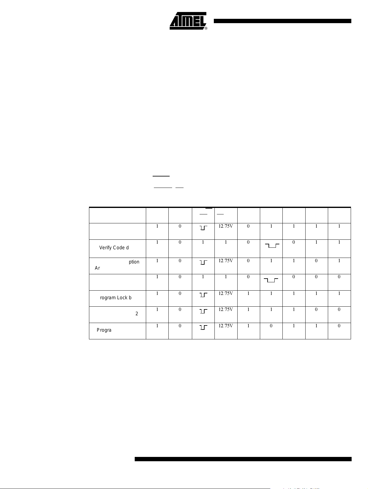
17.3.1 Set-up modes
In order to program and verify the EP ROM or t o read the signature bytes, the TS87 C54/5 8X2 is
placed in specific set-up modes (See Figure 17-1.).
Control and program signals must be held at the levels indicated in Table 17-2.
17.3.2 Definition of terms
Address Lines:P1.0-P1.7, P2.0-P2.5, P3.4 respectively for A0-A14 (P2.5 (A13) for
TS87C54X2, P3.4 (A14) for TS87C58X2).
Data Li nes:P0.0-P0.7 for D0-D7
Control Signals:RST, PSEN
Program Signals : ALE/PROG
, P2.6 , P2.7, P3.3, P3 .6, P3 . 7 .
, EA/VPP.
Table 17-2. EPROM Set-Up Modes
Mode RST PSEN
Program Code data
Verify Code data
Program Encryption
Array Address 0-3 Fh
Read Signature Bytes
Program Lock bit 1
Program Lock bit 2
Program Lock bit 3
10 12.75V01111
10110 011
1 0 12.75V 0 1 1 0 1
1 0 1 1 0 0 0 0
1 0 12.75V 1 1 1 1 1
1 0 12.75V 1 1 1 0 0
1 0 12.75V 1 0 1 1 0
ALE/PR
OG EA/VPP P2.6 P2.7 P3.3 P3.6 P3.7
38
AT/TS8xC54/8X2
4431E–8051–04/06

Figure 17-1. Set-Up Modes Configuration
EA
PROGRAM
SIGNALS*
/VPP
ALE/PROG
VCC
AT/TS8xC54/8X2
+5V
CONTROL
SIGNALS*
4 to 6 MHz
* See Table 31. for proper value on these inputs
17.3.3 Programming Algorithm
The Improved Q uick Pulse algorithm is based on the Qui ck Pulse algo rithm and de creases th e
number of pulses applied during byte programming from 25 to 1.
To program the TS80C54/58X2 the following sequen ce must be exercised:
• Step 1: Activate the combination of control signals.
• Step 2: Input the valid address on the address lines.
• Step 3: Input the appropriate data on the data lines.
• Step 4: Raise EA
• Step 5: Pulse ALE/PROG
• Step 6: Lower EA
Repeat s tep 2 throu gh 6 c han ging the a ddres s and da ta for th e ent ire ar ray o r unt il the end of
the object file is reached (See Figure 17-2.).
RST
PSEN
P2.6
P2.7
P3.3
P3.6
P3.7
XTAL1
P0.0-P0.7
P1.0-P1.7
P2.0-P2.5,
VSS
GND
D0-D7
A0-A7
A8-A14
/VPP from VCC to VPP (typical 12.75V).
once.
/VPP from VPP to VCC
17.3.4 Verify algorithm
4431E–8051–04/06
Code array verify must be done after each byte or block of by tes is programm ed. In either case,
a complete verify of the programmed array will ensure reliable programming of the
TS87C54/58X2.
P 2.7 is used to enable data output.
To verify the TS87C54/58X2 code the following sequence must be exercised:
• Step 1: Activate the combination of program and control signals.
• Step 2: Input the valid address on the address lines.
• Step 3: Read data on the data lines.
Repeat step 2 through 3 changing the address for the entire array verification (See Figure 17-2.)
39

The enc ryption a rray cann ot be di rectl y verif ied. Veri fica tion of t he en crypti on array is do ne by
observing that the code array is well encrypted.
Figure 17-2. P rogram m ing and Verification Signal’s Wavef orm
Progr amming Cycle
A0-A12
D0-D7
ALE/PROG
EA/VPP
Control
signals
12.75V
5V
0V
Data In
100μs
17.4 EPROM Erasure (Windowed Packages Only)
Erasing the EPR OM erases the c ode array, the encry ption array and t he lock bits returning th e
parts to full functionality.
Erasure leaves all the EPROM cells in a 1’s state (FF).
17.4.1 Erasure Characteristics
The recommended erasure procedure is exposure to ultraviolet light (at 2537 Å) to an integrated
dose at least 15 W-s ec/cm
ing for 30 minutes , at a distance of about 25 mm, should be sufficient. An exposu re of 1 hour is
recommended with most of standard erasers.
2
. Exposing the E P ROM to an ultraviolet l amp of 12,000 μW/cm2 rat-
Read/Verify Cycle
Data Out
Erasure of the EPR OM begins to occur wh en the chip i s exposed to light w ith wavelen gth
shorter than approximately 4,000 Å. Since sunli ght and fluoresce nt lighting have wavel engt hs in
this range, exposure to these light sources over an extended time (about 1 week in sunlight, or 3
years in room-leve l fluores cent lightin g) could c ause inad vertent eras ure. If an applicat ion subjects the device to this type of exposure, it is suggested that an opaque label be placed over the
window.
18. Signature Bytes
The TS87C54/58X2 has four signature bytes in location 30h, 31h, 60h and 61h. To read these
bytes follow the p rocedure f or E PR OM ve rify but ac tivate the c ontrol l ines p ro vided in T able 31.
for Read Signature Byte s. Table 18-1. shows the content of the signature by te for the
TS80C54/58X2.
40
AT/TS8xC54/8X2
4431E–8051–04/06

Table 18-1. Signature Bytes Content
Location Contents Comment
30h 58h
31h 57h Family Code: C51 X2
60h 37h Product name: TS80C58X2
60h B7h Product name: TS87C58X2
60h 3Bh Product name: TS80C54X2
60h BBh Product name: TS87C54X2
61h FFh Product revision number
AT/TS8xC54/8X2
Manuf acturer Code: Atmel Wireless &
Microcontrollers
4431E–8051–04/06
41

19. Electrical Characteristics
19.1 Absolute Maximum Rating s
(1)
Ambiant Temperature Under Bias:
C = commercial0°C to 70°C
I = industrial -40°C to 85°C
Storage Temperature-65°C to + 150°C
Voltage on V
Voltage on V
Voltage on Any Pin to V
Power Dissipation1 W
to VSS-0.5 V to + 7 V
CC
to VSS-0.5 V to + 13 V
PP
SS
(2)
1. Stresses at or above those listed under “ Absolute Maximum Ratings” may cause permanent damage to the device. This is a stress rating only and functional operation of
the device at these or any other conditions above those indicated in the operational
sections of this specification is not implied. Exposure to absolute maximum rating conditions may affect device reliability.
2. This value is based on the maximum allowable die temp erature and the thermal resistance of the package.
19.2 Power consumption measurement
Since the introduction of the first C51 devices, every manufacturer made operating Icc measurements under reset, which made sense for the designs were the CPU was running under reset. In
Atmel new devices , the CPU is no more a ctive durin g rese t, so the pow er con sumpt ion is very
low but is not really representative of what will happen in the customer system. That’s why, while
keeping measurements under Reset, Atmel presents a new way to measure the operating Icc:
-0.5 V to VCC + 0.5 V
Using an internal test ROM, the following code is executed:
Label: SJMP Label (80 FE)
Ports 1, 2 , 3 ar e disc onne cted , Port 0 is t ied to FFh , EA = Vcc, R ST = Vss, XTA L2 is not co n-
nected and XTAL1 is driven by the clock.
This is much more representative of the real operating Icc.
19.3 DC Parameters for Standard Voltage
TA = 0°C to +7 0°C; VSS = 0 V; VCC = 5 V ± 10%; F = 0 to 40 MHz.
A = -40°C to +85°C; V
T
Table 19-1. DC Parameters in Standard Voltage
Symbol Parameter Min Typ Max Unit Test Conditions
V
V
V
V
Input Low Voltage -0.5 0.2 VCC - 0.1 V
IL
Input High Voltage except XTAL1, RST 0.2 VCC + 0.9 VCC + 0.5 V
IH
Input High Voltage, XTAL1, RST 0.7 V
IH1
Output Low Voltage, ports 1, 2, 3
OL
(6)
= 0 V; VCC = 5 V ± 10%; F = 0 to 40 MHz.
SS
CC
VCC + 0.5 V
0.3
0.45
1.0
V
V
V
= 100 μA
I
OL
IOL = 1.6 mA
IOL = 3.5 mA
(4)
(4)
(4)
42
AT/TS8xC54/8X2
4431E–8051–04/06

AT/TS8xC54/8X2
Symbol Parameter Min Typ Max Unit Test Conditions
CC <
(4)
(4)
(4)
(4)
(4)
(4)
CC
5.5 V
(1)
(8)
(2)
V
OL1
V
OL2
V
OH
V
OH1
V
OH2
R
RST
I
IL
I
LI
I
TL
C
IO
I
PD
I
CC
under
RESET
I
CC
operating
I
CC
idle
Output Low Voltage, port 0
(6)
Output Low Voltage, ALE, PSEN
V
- 0.3
CC
Output High Voltage, ports 1, 2, 3
Output High Voltage, port 0
- 0.7
V
CC
- 1.5
V
CC
- 0.3
V
CC
V
- 0.7
CC
- 1.5
V
CC
VCC - 0.3
Output High Voltage,ALE, PSEN
- 0.7
V
CC
- 1.5
V
CC
RST Pulldown Resistor 50 90
0.3
0.45
1.0
0.3
0.45
1.0
(5)
200 kΩ
V
V
V
V
V
V
V
V
V
V
V
V
V
V
V
= 200 μA
I
OL
IOL = 3.2 mA
IOL = 7.0 mA
= 100 μA
I
OL
IOL = 1.6 mA
IOL = 3.5 mA
= -10 μA
I
OH
= -30 μA
I
OH
= -60 μA
I
OH
= 5 V ± 10%
V
CC
I
= -200 μA
OH
= -3.2 mA
I
OH
I
= -7.0 mA
OH
= 5 V ± 10%
V
CC
= -100 μA
I
OH
= -1.6 mA
I
OH
= -3.5 mA
I
OH
= 5 V ± 10%
V
CC
Logical 0 Input Current ports 1, 2 and 3 -50 μA Vin = 0.45 V
Input Leakage C urrent ±10 μA 0.45 V < Vin < V
Logical 1 to 0 Transition Current, ports 1, 2, 3 -650 μA Vin = 2.0 V
Capacitanc e of I/O Buffer 10 pF
Power Down Current 20
(5)
50 μA2.0 V < V
Fc = 1 MHz
T
A = 25°C
1 + 0.4 Freq
Power Supply Current Maximum values, X1
(7)
mode:
(MHz)
@12MHz 5.8
@16MHz 7.4
mA
V
CC
= 5.5 V
3 + 0.6 Freq
Power Supply Current Maximum values, X1
(7)
mode:
(MHz)
@12MHz 10.2
@16MHz 12.6
mA V
= 5.5 V
CC
0.25+0 .3 Fr e q
Power Supply Current Maximum values, X1
(7)
mode:
(MHz)
@12MHz 3.9
mA
V
CC
= 5.5 V
@16MHz 5.1
(3)
4431E–8051–04/06
43

19.4 DC Parameters for Low Voltage
TA = 0°C to +7 0°C; VSS = 0 V; VCC = 2.7 V to 5.5 V ± 10%; F = 0 to 30 MHz.
A = -40°C to +85°C; V
T
Table 19-2. DC Parameters for Low Voltage
Symbol Parameter Min Typ Max Unit Test Conditions
V
V
V
IH1
V
V
OL1
V
OH
V
OH1
I
I
I
TL
R
RST
CIO Capacitance of I/O Buffer 10 pF
Input Low Voltage -0.5 0.2 VCC - 0.1 V
IL
Input High Voltage except XTAL1, RST 0.2 VCC + 0.9 VCC + 0.5 V
IH
Input High Voltage, XTAL1, RST 0.7 V
Output Low Voltage, ports 1, 2, 3
OL
Output Low Voltage, port 0, ALE, PSEN
(6)
(6)
Output High Voltage, ports 1, 2, 3 0.9 V
Output High Voltage, port 0, ALE, PSEN 0.9 V
Logica l 0 Input Current ports 1, 2 and 3 -50 μAVin = 0.45 V
IL
Input Le ak ag e C urr e n t ±10 μA 0.45 V < Vin < V
LI
Logica l 1 to 0 Transition Current, ports 1, 2, 3 -650 μAVin = 2.0 V
RST Pulldown Resistor 50 90
= 0 V; VCC = 2.7 V to 5.5 V ± 10%; F = 0 to 30 MHz.
SS
CC
VCC + 0.5 V
0.45 V IOL = 0.8 mA
0.45 V IOL = 1.6 mA
CC
CC
(5)
200 kΩ
VIOH = -10 μA
VIOH = -40 μA
Fc = 1 MHz
T
A = 25°C
(4)
(4)
CC
I
PD
I
CC
under
RESET
Power Down Current
Power Supply Current Maximum values, X1
(7)
mode:
20
10
(5)
50
30
1 + 0.2 Freq
(MHz)
@12MHz 3.4
@16MHz 4.2
VCC = 2.0 V to 5.5 V
μA
VCC = 2.0 V to 3.3 V
= 3.3 V
V
mA
CC
(5)
1 + 0.3 Freq
I
CC
operating
Power Supply Current Maximum values, X1
(7)
mode:
(MHz)
@12MHz 4.6
@16MHz 5.8
mA
V
CC
= 3.3 V
0.15 Freq (MHz)
I
CC
idle
Power Supply Current Maximum values, X1
(7)
mode:
+ 0.2
@12MHz 2
mA V
= 3.3 V
CC
@16MHz 2.6
1. I
2. Idle I
3. Power Down I
under reset is measured with all output pins disconnected; XTAL1 driven with T
CC
19-5.), V
V
= VCC - 0.5V; XTAL2 N.C.; EA = RST = Port 0 = VCC. ICC would be slightly higher if a crystal oscillator used..
IH
V
= V
IH
= VSS + 0.5 V,
IL
is measured with all output pins disconnected; XTAL1 driven with T
CC
- 0.5 V; XTAL2 N.C; Port 0 = VCC; EA = RST = VSS (see Figure 19-3.).
CC
is measured with all output pins disconnected; EA = VSS, PORT 0 = VCC; XTAL2 NC.; RS T = VSS
CC
CLCH
, T
, T
CLCH
= 5 ns, VIL = VSS + 0.5 V,
CHCL
= 5 ns (see Figure
CHCL
(see Figure 19-4.).
4. Capacitance loading on Ports 0 and 2 may cause spurious noise pulses to be superimposed on the V
s of ALE
OL
and Ports 1 and 3. The noise is due to external bus capacitance discharging into the Port 0 and Port 2 pins when
these pins make 1 to 0 transitions during bus operation. In the worst cases (capacitive loading 100pF), the noise
pulse on the ALE line may exceed 0.45V with maxi V
peak 0.6V. A Schmitt Trigger use is not necessary.
OL
(3)
(3)
(1)
(8)
(2)
44
AT/TS8xC54/8X2
4431E–8051–04/06

AT/TS8xC54/8X2
5. Typicals are based on a limited number of samples and are not guaranteed. The values listed are at room temperature and 5V.
6. Under steady state (non-transient) conditions, I
Maximum I
Maximum I
per port pin: 10 mA
OL
per 8-bit port:
OL
Port 0: 26 mA
Ports 1, 2 and 3: 15 mA
Maximu m total I
If I
exceeds the test condition, VOL may exceed the related specification. Pins are not guaranteed to sink current
OL
for all output pins: 71 mA
OL
greater than the listed test conditions.
7. For other values, please contact your sales office.
8. Operating I
19-5.), V
V
= VCC - 0.5V; XTAL2 N.C.; EA = Port 0 = VCC; RST = VSS. The internal ROM runs the code 80 FE (label: SJMP
IH
label). I
is measured with all output pins disconnected; XTAL1 driven with T
CC
= VSS + 0.5 V,
IL
would be slightly higher if a crystal oscillator is used. Measurements are made with OTP products when
CC
possible, which is the worst case.
Figure 19-1. ICC Test Condition, under reset
must be externally limited as follows:
OL
CLCH
, T
= 5 ns (see Figure
CHCL
(NC)
CLOCK
SIGNAL
Figure 19-2. Operating I
Reset = Vss after a high pulse
during at least 24 clock cycles
V
CC
RST
XTAL2
XTAL1
V
SS
Test Condition
CC
RST
V
CC
I
CC
V
CC
V
CC
P0
EA
All other pins are disconnected.
V
CC
I
CC
V
CC
V
CC
P0
EA
4431E–8051–04/06
(NC)
CLOCK
SIGNAL
XTAL2
XTAL1
V
SS
All other pins are disconnected.
45

Figure 19-3. ICC Test Condition, Idle Mode
I
CC
V
CC
Reset = Vss after a high pulse
during at least 24 clock cycles
RST
P0
EA
V
CC
V
CC
Figure 19-4. I
Reset = Vss after a high pulse
during at least 24 clock cycles
CC
(NC)
CLOCK
SIGNAL
Test Condition, Power-Down Mode
(NC)
RST
XTAL2
XTAL2
XTAL1
V
SS
V
CC
EA
I
P0
CC
V
CC
V
XTAL1
V
SS
Figure 19-5. Cl oc k Signal Waveform for I
All other pins are disconnected.
CC
All other pins are disconnected.
Tests in Active and Idle Modes
CC
46
VCC-0.5V
AT/TS8xC54/8X2
0.45V
T
CHCL
T
CLCH
= T
CHCL
T
CLCH
= 5ns.
0.7V
CC
0.2VCC-0.1
4431E–8051–04/06

19.5 A C Parameters
19.5.1 Explanation of the AC Symbols
Each timing sy mbo l has 5 cha racters. Th e first cha racter i s always a “T ” (stand s for time). The
other characters, depending on their positions, stand for the name of a signal or the logical status of that signal. The following is a list of all the characters and what they stand for.
AT/TS8xC54/8X2
Example:T
T
LLPL
T
A = 0 to +70°C (commercial temperature range); V
A = -40°C to +85°C (industrial temperature range); V
T
= Time for Address Valid to ALE Low.
AVLL
= Time for ALE Low to PSEN Low.
= 0 V; VCC = 5 V ± 10%; -M and -V ranges.
SS
= 0 V; VCC = 5 V ± 10%; -M and -V
SS
ranges.
A = 0 to +70°C (commercial temperature range); V
T
A = -40°C to +85°C (industrial temperature range); V
T
= 0 V; 2.7 V < V
SS
= 0 V; 2.7 V < V
SS
5.5 V; -L range.
CC <
5.5 V; -L range.
CC <
Table 19-3. gives the maximum applicable load capacitance for Port 0, Port 1, 2 and 3, and ALE
and PSEN
signals. Timings will be guaranteed if these capacitanc es are respected. Higher
capacitance values can be used, but timings will then be degraded.
Table 19-3. Load Capacitance versus speed range, in pF
-M -V -L
Port 0 100 50 100
Port 1, 2, 3 80 50 80
ALE / PSEN 100 30 100
Table 19-5., Table 19-8. and Table 19-11. give the description of each AC symbols.
Table 19-6., Table 19-9. and Table 19-12. give for each range the AC parameter.
4431E–8051–04/06
Table 19-7., Ta ble 19-10. and Tab le 19-13. give the frequ ency derating form ula of the AC
paramet er. To cal culate e ach AC sy mb ols, ta ke th e x va lue co rresp ondi ng to t he spee d g rade
you need ( -M, -V o r -L) and re plac e this val ue in the form ula. Valu es of the frequ ency m ust b e
limited to the corresponding speed grade:
Table 19-4. Max frequency for derating formula regarding the speed grade
-M X1 mode -M X2 mode -V X1 mode -V X2 mode -L X1 mode -L X2 mode
Freq (MHz) 40 20 40 30 30 20
T (ns) 25 50 25 33.3 33.3 50
Example:
in X2 mode for a -V part at 20 MHz (T = 1/20E6 = 50 ns):
T
LLIV
x= 22 (Table 19-7.)
T= 50ns
T
= 2T - x = 2 x 50 - 22 = 78ns
LLIV
47
19.5.2 External Prog ram Memo ry Char acteri stics
Table 19-5. Symbol Description
Symbol Parameter
T Oscillat or clock pe riod
T
LHLL
T
AVLL
T
LLAX
T
LLIV
T
LLPL
T
PLPH
T
PLIV
T
PXIX
T
PXIZ
T
PXAV
T
AVIV
T
PLAZ
ALE pulse width
Address Valid to ALE
Addr es s Hold After ALE
ALE to Valid In struc tion In
ALE to PSEN
PSEN Pulse Width
PSEN to Valid Instruction In
Input Instru c tio n Hold After PSEN
Input Instruc tion Float After PSEN
PSEN to Address Valid
Address to Valid Instru c tio n In
PSEN Low to Address Float
Table 19-6. AC Parameters for Fix Clock
Speed
-M
40 MHz
-V
X2 mode
30 MHz
60 MHz equiv.
standard mode 40
-V
MHz
Symbol Min Max Min Max Min Max Min Max Min Max
T2533255033 ns
T
T
T
T
T
T
T
T
T
T
T
LHLL
AVLL
LLAX
LLIV
LLPL
PLPH
PLIV
PXIX
PXIZ
AVIV
PLAZ
40 25 42 35 52 ns
10 4 12 5 13 ns
10 4 12 5 13 ns
70 45 78 65 98 ns
15 9 171018 ns
55 35 60 50 75 ns
35 25 50 30 55 ns
00000 ns
18 12 20 10 18 ns
85 53 95 80 122 ns
10 10 10 10 10 ns
-L
X2 mode
20 MHz
40 MHz equiv.
-L
standard mo d e
30 MHz Units
48
AT/TS8xC54/8X2
4431E–8051–04/06

AT/TS8xC54/8X2
Table 19-7. AC Parameters for a Variable Clock: derating formula
Symbol Type
T
T
T
T
T
T
T
T
T
T
T
LHLL
AVLL
LLAX
LLIV
LLPL
PLPH
PLIV
PXIX
PXIZ
AVIV
PLAZ
Min 2 T - x T - x 10 8 15 ns
Min T - x 0.5 T - x 15 13 20 ns
Min T - x 0.5 T - x 15 13 20 ns
Max 4 T - x 2 T - x 30 22 35 ns
Min T - x 0.5 T - x 10 8 15 ns
Min 3 T - x 1.5 T - x 20 15 25 ns
Max 3 T - x 1.5 T - x 40 25 45 ns
Minxx000 ns
Max T - x 0.5 T - x 7 5 15 ns
Max 5 T - x 2.5 T - x 40 30 45 ns
Max x x 10 10 10 ns
19.5.3 External Prog ram Memo ry Read Cycle
Figure 19-6. E x ternal Program M emory Read Cycle
T
ALE
PSEN
PORT 0
LHLL
T
LLAX
T
AVLL
Standard
Clock X2 Clock -M -V -L Units
12 T
CLCL
T
LLIV
T
LLPL
T
PLPH
T
PXAV
T
PLIV
TPLAZ
T
PXIX
T
PXIZ
A0-A7A0-A7 INSTR ININSTR IN INSTR IN
4431E–8051–04/06
PORT 2
ADDRESS
OR SFR-P2
T
AVIV
ADDRESS A8-A15ADDRESS A8-A15
49

19.5.4 External Data Memory Characteri stics
Table 19-8. Symbol Description
Symbol Parameter
T
T
WLWH
T
T
T
T
T
T
T
T
QVWX
T
QVWH
T
WHQX
T
T
RLRH
RLDV
RHDX
RHDZ
LLDV
AVDV
LLWL
AVWL
RLAZ
WHLH
RD Pulse Width
WR Pulse Width
RD to Valid Data In
Data Hold After RD
Data Float After RD
ALE to Valid Data In
Address to Valid Data In
ALE to WR or RD
Address to WR or RD
Data Valid to WR Transition
Data set-up to WR High
Data Hold After WR
RD Low to Address Float
RD or WR High to ALE high
Table 19-9. AC Parameters for a Fix Clock
Speed -M
40 MHz
-V
X2 mode
30 MHz
60 MHz equiv.
standard mode 40
-V
MHz
Symbol Min Max Min Max Min Max Min Max Min Max
T
T
T
T
T
T
T
T
T
T
T
T
T
T
RLRH
WLWH
RLDV
RHDX
RHDZ
LLDV
AVDV
LLWL
AVWL
QVWX
QVWH
WHQX
RLAZ
WHLH
130 85 135 125 175 ns
130 85 135 125 175 ns
100 60 102 95 137 ns
00000 ns
30 18 35 25 42 ns
160 98 165 155 222 ns
165 100 175 160 235 ns
50100307055954510570130 ns
75 47 80 70 103 ns
10 7 15 5 13 ns
160 107 165 155 213 ns
15 9 171018 ns
00000ns
104072715355451353 ns
-L
X2 mode
20 MHz
40 MHz equiv.
-L
standard mo d e
30 MHz
Units
50
AT/TS8xC54/8X2
4431E–8051–04/06

AT/TS8xC54/8X2
Table 19-10. AC Parameters for a Variable Clock: derating formula
Symbol Type
T
T
WLWH
T
T
T
T
T
T
T
T
T
QVWX
T
QVWH
T
WHQX
T
T
T
RLRH
RLDV
RHDX
RHDZ
LLDV
AVDV
LLWL
LLWL
AVWL
RLAZ
WHLH
WHLH
Min 6 T - x 3 T - x 20 15 25 ns
Min 6 T - x 3 T - x 20 15 25 ns
Max 5 T - x 2.5 T - x 25 23 30 ns
Minxx000 ns
Max 2 T - x T - x 20 15 25 ns
Max 8 T - x 4T -x 40 35 45 ns
Max 9 T - x 4.5 T - x 60 50 65 ns
Min 3 T - x 1.5 T - x 25 20 30 ns
Max 3 T + x 1.5 T + x 25 20 30 ns
Min 4 T - x 2 T - x 25 20 30 ns
Min T - x 0.5 T - x 15 10 20 ns
Min 7 T - x 3.5 T - x 15 10 20 ns
Min T - x 0.5 T - x 10 8 15 ns
Maxxx000 ns
Min T - x 0.5 T - x 15 10 20 ns
Max T + x 0.5 T + x 15 10 20 ns
Standard
Clock X2 Clock -M -V -L Units
19.5.5 External Data Memory Write Cycle
Figure 19-7. External Data Memory Write Cycle
ALE
PSEN
WR
PORT 0
PORT 2
ADDRESS
OR SFR-P2
T
LLAX
T
LLWL
T
QVWX
T
T
QVWH
WLWH
A0-A7 DATA OUT
T
AVWL
ADDRESS A8-A15 OR SFR P2
T
WHLH
T
WHQX
4431E–8051–04/06
51

19.5.6 External Data Memory Read Cycle
Figure 19-8. External Data Memory Read Cycle
ALE
T
LLDV
T
WHLH
PSEN
RD
PORT 0
PORT 2
ADDRESS
OR SFR-P2
A0-A7 DATA IN
19.5.7 Serial Port Timing - Shift Register Mode
Table 19-11. Symbol Description
Symbol Parameter
T
XLXL
T
QVHX
T
XHQX
T
XHDX
T
XHDV
Table 19-12. AC Parameters for a Fix Clock
-V
X2 mode
Speed
-M
40 MHz
30 MHz
60 MHz equiv.
T
LLWL
T
T
LLAX
T
AVWL
AVDV
-V
standard mode 40
MHz
T
RLRH
T
T
RLDV
RLAZ
ADDRESS A8-A15 OR SFR P2
Serial port clock cycle time
Output data set-up to clock rising edge
Output data hold after clock rising edge
Input data hold after clock rising edge
Clock r is in g ed ge to inpu t da ta val id
-L
X2 mode
20 MHz
40 MHz equiv.
T
RHDX
-L
standard mo d e
30 MHz
T
RHDZ
Units
Symbol Min Max Min Max Min Max Min Max Min Max
300 200 300 300 400 ns
200 117 200 200 283 ns
30 13 30 30 47 ns
00000 ns
117 34 117 117 200 ns
52
T
XLXL
T
QVHX
T
XHQX
T
XHDX
T
XHDV
AT/TS8xC54/8X2
4431E–8051–04/06

AT/TS8xC54/8X2
Table 19-13. AC Parameters for a Variable Clock: derating formula
Symbol Type
T
XLXL
T
QVHX
T
XHQX
T
XHDX
T
XHDV
19.5.8 Shift Register Timing Waveforms
Figure 19-9. Shift Register Timing Waveforms
INSTRUCTION
ALE
CLOCK
OUTPUT DATA
WRITE to SBUF
INPUT DATA
CLEAR RI
0123456 87
T
XLXL
T
QVXH
01234567
T
XHDV
Standard
Clock X2 Clock -M -V -L Units
Min 12 T 6 T ns
Min 10 T - x 5 T - x 50 50 50 ns
Min 2 T - x T - x 20 20 20 ns
Minxx000 ns
Max 10 T - x 5 T- x 133 133 133 ns
T
XHQX
T
XHDX
VALIDVAL ID
VALIDVALID
VAL ID VA LI D VA LID VA LI D
SET TI
SET RI
4431E–8051–04/06
53

19.5.9 EPROM Programming and Verification Characteristics
T
A = 21°C to 27°C; V
verifying
.
= 0V; VCC = 5V ± 10% while programming. VCC = operating range while
SS
Table 19-14. EPROM Programming Parameters
Symbol Parameter Min Max Units
1/T
T
T
T
T
T
T
T
T
T
T
V
I
T
AVGL
GHAX
DVGL
GHDX
EHSH
SHGL
GHSL
GLGH
AVQV
ELQV
EHQZ
PP
PP
CLCL
Programming Supply Voltage 12.5 13 V
Progra mm in g S up p ly Cur r en t 75 mA
Oscillator Frquency 4 6 MHz
Address Setup to PROG Low 48 T
Adress Hold after PROG 48 T
Data Setup to PROG Low 48 T
Data Hold after PROG 48 T
(Enable) Hi g h to V
VPP Setup to PROG Low 10 μs
PP
VPP Hold after PROG 10 μs
PROG Width 90 110 μs
Address to Valid Data 48 T
ENABLE Low to Data Valid 48 T
Data Float after ENAB LE 0 48 T
48 T
CLCL
CLCL
CLCL
CLCL
CLCL
CLCL
CLCL
CLCL
19.5.10 EPROM Programming and Verification Waveforms
Figure 19-10. EPROM Programming and Verification Waveforms
PROGRAMMING
P1.0-P1.7
P2.0-P2.5
P3.4-P3.5*
P
P0
T
DVGL
T
AVGL
ALE/PROG
T
SHGL
T
GLGH
EA/V
PP
V
CC
CONTROL
SIGNALS
(ENABLE)
* 8KB: up to P2.4, 16KB: up to P2.5, 32KB: up to P3.4, 64KB: up to P3.5
T
EHSH
ADDRESS
DATA IN
V
PP
T
GHDX
T
T
GHAX
GHSL
VERIFICATION
ADDRESS
T
AVQV
DATA OUT
V
CC
T
ELQV
T
EHQZ
54
AT/TS8xC54/8X2
4431E–8051–04/06
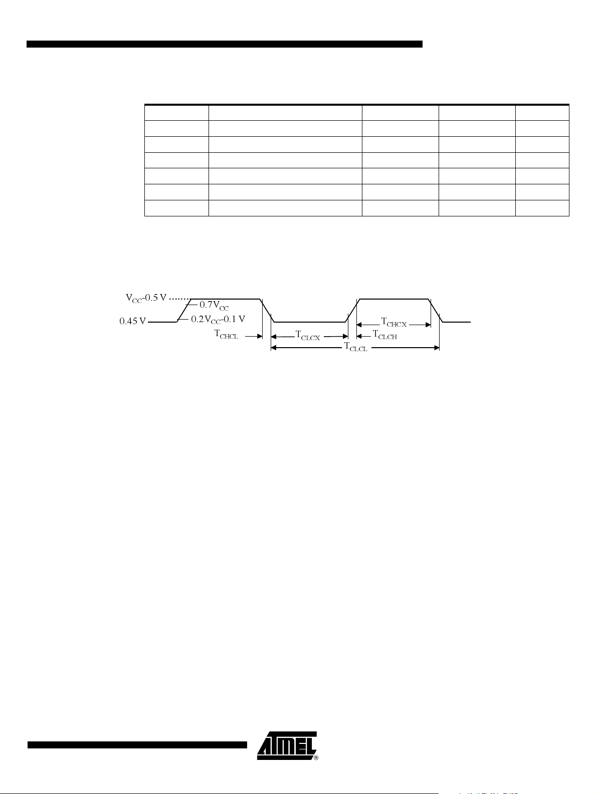
19.5.11 External Clock Drive Characteristics (XTAL1) Table 19-15. AC Parameter s
Symbol Parameter Min Max Units
T
CLCL
T
CHCX
T
CLCX
T
CLCH
T
CHCL
T
CHCX/TCLCX
Oscillat or Per i od 25 ns
High Time 5 ns
Low Time 5 ns
Rise Time 5 ns
Fall Time 5 ns
Cyclic ratio in X2 mode 40 60 %
19.5.12 External Clock Drive Waveforms
Figure 19-11. External Clock Drive Waveforms
AT/TS8xC54/8X2
VCC-0.5 V
V
0.45
0.7V
CC
0.2VCC-0.1 V
T
CHCL
T
CLCX
T
CLCL
T
T
CHCX
CLCH
4431E–8051–04/06
55

19.5.13 AC Testing Input/Output Waveforms
Figure 19-12. AC Testing Input/Ou tpu t Waveforms
V
-0.5 V
CC
INPUT/OUTPUT
0.45 V
0.2V
0.2V
CC
CC
+0.9
-0.1
AC inputs during testing are driven at V
measurement are made at V
19.5.14 Float Waveforms
Figure 19-13. Float Waveforms
For tim ing pu rpos es a por t pi n is no l on ger fl oat ing whe n a 100 mV c ha nge from lo ad v ol tage
occurs and begins to float when a 100 mV c hang e from the loaded V
≥ ± 20mA.
19.5.15 Clock Waveforms
Valid in normal clock mode. In X2 mode XTAL2 signal must be changed to XTAL2 divided by
two.
-0.1 V
V
OH
VOL+0.1 V
FLOAT
V
LOAD
- 0.5 for a logi c “1” and 0.4 5V for a l ogic “0”. Timin g
CC
min for a logic “1” and VIL max for a logic “0”.
IH
V
+0.1 V
LOAD
V
-0.1 V
LOAD
OH/VOL
level occurs. IOL/I
OH
56
AT/TS8xC54/8X2
4431E–8051–04/06

Figure 19-14. Clock Waveforms
)
AT/TS8xC54/8X2
INTERNAL
CLOCK
XTAL2
ALE
EXTERNAL PROG RA M MEMORY FETCH
PSEN
P0
P2 (EXT)
READ CYCLE
RD
P0
P2
WRITE CYCLE
WR
P0
STATE4 STATE5 STATE6
P1P2 P1P2
DATA
SAMPLED
FLOAT FLOAT
PCL OUT
INDICATES ADDRESS
DPL OR Rt
DPL OR Rt OUT
P1P2
INDICA TES DPH OR P2 SFR TO PCH
TRANSITION
STATE1 STATE2 STATE3 STATE4
P1P2 P1P2 P1P2
THESE SIGNALS ARE NOT ACTIVATED DURING THE
EXECUTION OF A MOVX INSTRUCTION
DATA
SAMPLED
PCL O UT
SAMPLED
FLOAT
FLOAT
STATE5
P1P2 P1P2
DATA
PCL OUT (EVEN IF PROGRAM
MEMORY IS INTERNAL)
PCL OUT
PCL OUT (IF PROGRAM
MEMORY IS EXTERNAL)
P2
PORT OPERATION
P0 PINS SAMPLED
MOV DEST P0
MOV DEST PORT (P1, P2, P3)
(INCLUDES INT0, INT1, TO, T1)
SERIAL PORT SHIFT CLOCK
TXD (MODE 0)
This diagram indicates when signals are clocked internally. The time it takes the signals to propagate to th e pins, howev er, ranges from 2 5 to 12 5 ns. T his propa gati on dela y is de penden t on
variables such as temperature and pin loading. Propagation also varies from output to output
and component. Typically though (T
approximately 50 ns. The other signa ls are typically 85 ns . Propagation del ays are incorporat ed
in the AC specifications.
DATA OUT
INDICATES DPH OR P2 SFR TO PCH
TRANSITION
OLD DATA
P1, P2, P3 PINS SAMPLED
RXD SAMPLED RXD SAMPLED
NEW DATA
P1, P2, P3 PINS SAMPLED
=25°C fully loaded) RD and WR propagation delays are
A
PCL OUT (IF PROGRAM
MEMORY IS EX TE RNAL
P0 PINS SAMPLED
4431E–8051–04/06
57

20. Ordering Information
Table 20-1. P os sible Orde ring Entries
Part Number Supply Voltage Temperature Range Package Packing
TS80C54X2xxx-MCA -5 to +/-10% Commercial PDIL40 Stick
TS80C54X2xxx-MCB -5 to +/-10% Commercial PLCC44 Stick
TS80C54X2xxx-MCC -5 to +/-10% Commercial PQFP44 Tray
TS80C54X2xxx-MCE -5 to +/-10% Commercial VQFP44 Tray
TS80C54X2xxx-VCA -5 to +/-10% Commercial PDIL40 Stick
TS80C54X2xxx-VCB -5 to +/-10% Commercial PLCC44 Stick
TS80C54X2xxx-VCC -5 to +/-10% Commercial PQFP44 Tray
TS80C54X2xxx-VCE -5 to +/-10% Commercial VQFP44 Tray
TS80C54X2xxx-LCA -5 to +/-10% Commercial PDIL40 Stick
TS80C54X2xxx-LCB -5 to +/-10% Commercial PLCC44 Stick
TS80C54X2xxx-LCC -5 to +/-10% Commercial PQFP44 Tray
TS80C54X2xxx-LCE -5 to +/-10% Commercial VQFP44 Tray
TS80C5 4X2xxx-MIA -5 to +/- 10% Industrial PDIL40 Stick
TS80C54X2xxx-MIB -5 to +/-10% Industrial PLCC44 Stick
TS80C54X2xxx-MIC -5 to +/-10% Industrial PQFP44 Tray
TS80C5 4X2xxx-MIE -5 to +/- 10% Industrial VQFP44 Tray
TS80C54X2xxx-VIA -5 to +/-10% Industrial PDIL40 Stick
TS80C54X2xxx-VIB -5 to +/-10% Industrial PLCC44 Stick
TS80C5 4X2xxx-VIC -5 to +/-10% Industrial PQFP44 Tray
TS80C54X2xxx-VIE -5 to +/-10% Industrial VQFP44 Tray
TS80C54X2xxx-LIA -5 to +/-10% Industrial PDIL40 Stick
TS80C54X2xxx-LIB -5 to +/-10% Industrial PLCC44 Stick
TS80C5 4X2xxx-LIC -5 to +/- 10% Industrial PQFP44 Tray
TS80C5 4X2xxx-LIE -5 to +/-10% Industrial VQFP44 Tray
AT80C54X 2zzz-3CSUM -5 to +/-10% Industrial & G reen PDIL40 Stick
AT80C54X2zzz-SLSUM -5 to +/-10% Industrial & Green PLCC44 Stick
AT80C54X2zzz-RLTUM -5 to +/-10% Industrial & Green VQFP44 Tray
AT80C54X2 zzz-3CSUL -5 to +/-10% Industrial & Green PDIL40 Stick
AT80C54X2zzz-SLSUL -5 to +/-10% Industrial & Green PLCC44 Stick
AT80C54X2zzz-RLTUL -5 to +/-10% Industrial & G reen VQFP44 Tray
AT80C54X2zzz-3CSUV -5 to +/-10% Industrial & Green PDIL40 Stick
AT80C54X2 zzz-SLSUV -5 to +/-10% Industrial & Green PLCC44 Stic k
AT80C54X2zzz-RLTUV -5 to +/-10% Industrial & Green VQFP44 Tray
TS87C54X2-MCA 5V ±10% Commercial PDIL40 Stick
TS87C54X2-MCB 5V ±10% Commercial PLCC44 Stick
58
AT/TS8xC54/8X2
4431E–8051–04/06

AT/TS8xC54/8X2
Part Numb er Supply Voltage Temperatu re Range Package Packing
TS87C5 4X2-MCC 5V ±10% Commerc ial PQFP44 Tray
TS87C54X2-MCE 5V ±10% Commerc ial VQFP44 Tray
TS87C54X2-VCA 5V ±10% Commercial PDIL40 Stick
TS87C5 4X2-VCB 5V ±10% Commercial PLCC44 Stick
TS87C54X2-VCC 5V ±10% Commercial PQFP44 Tray
TS87C54X2-VCE 5V ±10% Commercial VQFP44 Tray
TS87C5 4X2-LC A 2.7 t o 5. 5V C o mm ercial PDIL 40 Stick
TS87C5 4X2-LC B 2. 7 to 5.5V Comm e r ci al PL CC 4 4 Stick
TS87C 54 X 2-LCC 2.7 to 5.5V Co mm ercial PQFP 44 Tr ay
TS87C5 4X2-LC E 2. 7 to 5. 5V C o mm ercial VQFP 44 Tr ay
TS87C54X2-MIA 5V ±10% Industrial PDIL40 Stick
TS87C54X2-MIB 5V ±10% Industrial PLCC44 Stick
TS87C54X2-MIC 5V ±10% Industrial PQFP44 Tray
TS87C54X2-MIE 5V ±10% Industrial VQFP44 Tray
TS87C5 4X2-VIA 5V ±10% Industrial PDIL40 Stick
TS87C54X2-VIB 5V ±10% Industrial PLCC44 Stick
TS87C54X2-VIC 5V ±10% Industrial PQFP44 Tray
TS87C5 4X2-VIE 5V ±10% Industrial VQFP4 4 Tray
TS87C 54 X2-LIA 2.7 to 5.5V Indu s trial PDIL 40 Stick
TS87C 54 X2-LIB 2.7 to 5.5V Indu s trial PL CC 4 4 Stick
TS87C 54 X2-LIC 2.7 to 5.5V Indus trial PQFP 44 Tr ay
TS87C 54 X2-LIE 2.7 to 5.5V Indu s trial VQFP 44 Tr ay
AT87C54X2-3CSUM 5V ±10% Industri al & Green PDIL40 Stick
AT87C54X2-SLSUM 5V ±10% Industrial & Green PLCC44 Stick
AT87C54X2-RLTUM 5V ±10% Industrial & Green VQFP44 Tray
AT87C54X2-3CSUL 2.7 to 5.5V Industrial & Green PDIL40 Stick
AT87C54X2-S L SU L 2.7 to 5.5V Ind u str ial & Green PLCC44 Stick
AT87C54X2-R LTUL 2.7 to 5.5V Ind ustrial & Green VQ F P44 Tray
AT87C54X2-3CSUV 5V ±10% Industrial & Green PDIL40 Stick
AT87C54X2-SLSUV 5V ±10% Industrial & Green PLCC44 Stick
AT87C54X2-RLTUV 5V ±10% Industri al & Green VQFP44 Tray
4431E–8051–04/06
59

Part Numb er Supply Voltage Temperatu re Range Package Packing
TS80C58X2xxx-MCA -5 to +/-10% Commercial PDIL40 Stick
TS80C58X2xxx-MCB -5 to +/-10% Commercial PLCC44 Stick
TS80C58X2xxx-MCC -5 to +/-10% Commercial PQFP44 Tray
TS80C58X2xxx-MCE -5 to +/-10% Commercial VQFP44 Tray
TS80C58X2xxx-VCA -5 to +/-10% Commercial PDIL40 Stick
TS80C58X2xxx-VCB -5 to +/-10% Commercial PLCC44 Stick
TS80C58X2xxx-VCC -5 to +/-10% Commercial PQFP44 Tray
TS80C58X2xxx-VCE -5 to +/-10% Commercial VQFP44 Tray
TS80C58X2xxx-LCA -5 to +/-10% Commercial PDIL40 Stick
TS80C58X2xxx-LCB -5 to +/-10% Commercial PLCC44 Stick
TS80C58X2xxx-LCC -5 to +/-10% Commercial PQFP44 Tray
TS80C58X2xxx-LCE -5 to +/-10% Commercial VQFP44 Tray
TS80C58X2xxx-MIA -5 to +/-10% Industrial PDIL40 Stick
TS80C58X2xxx-MIB -5 to +/-10% Industrial PLCC44 Stick
TS80C58X2xxx-MIC -5 to +/-10% Industrial PQFP44 Tray
TS80C58X2xxx-MIE -5 to +/-10% Industrial VQFP44 Tray
TS80C58X2xxx-VIA -5 to +/-10% Industrial PDIL40 Stick
TS80C58X2xxx-VIB -5 to +/-10% Industrial PLCC44 Stick
TS80C58X2xxx-VIC -5 to +/-10% Industrial PQFP44 Tray
TS80C58X2xxx-VIE -5 to +/-10% Industrial VQFP44 Tray
TS80C58X2xxx-LIA -5 to +/-10% Industrial PDIL40 Stick
TS80C58X2xxx-LIB -5 to +/-10% Industrial PLCC44 Stick
TS80C58X2xxx-LIC -5 to +/-10% Industrial PQFP44 Tray
TS80C58X2xxx-LIE -5 to +/-10% Industrial VQFP44 Tray
AT80C58X2zzz-3CSUM -5 to +/-10% Industrial & Green PDIL40 Stick
AT80C58X2zzz-SLS UM -5 to +/-10% Industrial & Green PLCC44 Stick
AT80C58X2zzz-RLTUM -5 to +/-10% Industrial & Gre en VQFP44 Tray
AT80C58X2zzz-3CSUL -5 to +/-10% Industrial & Green PDIL40 Stick
AT80C58X2zzz-SLSUL -5 to +/-10% Industrial & Green PLCC44 Stick
AT80C58X2zzz-RLTUL -5 to +/-10% Industrial & Green VQFP44 Tray
AT80C58X2zzz-3CSUV -5 to +/-10% Industrial & Green PDIL40 Stick
AT80C58X2zzz-SLSUV -5 to +/-10% Industrial & Green PLCC44 Stick
AT80C58X2zzz-RLTUV -5 to +/-10% Industrial & Green VQFP44 Tray
TS87C58X2-MCA 5V ±10% Commerc ial PDIL40 Stick
TS87C5 8X2-MCB 5V ±10% Commercial PLCC44 Stick
TS87C5 8X2-MCC 5V ±10% Commerc ial PQFP44 Tray
60
AT/TS8xC54/8X2
4431E–8051–04/06

AT/TS8xC54/8X2
Part Numb er Supply Voltage Temperatu re Range Package Packing
TS87C58X2-MCE 5V ±10% Commerc ial VQFP44 Tray
TS87C58X2-VCA 5V ±10% Commercial PDIL40 Stick
TS87C5 8X2-VCB 5V ±10% Commercial PLCC44 Stick
TS87C58X2-VCC 5V ±10% Commercial PQFP44 Tray
TS87C58X2-VCE 5V ±10% Commercial VQFP44 Tray
TS87C5 8X2-LC A 2.7 t o 5. 5V C o mm ercial PDIL 40 Stick
TS87C5 8X2-LC B 2. 7 to 5.5V Comm e r ci al PL CC 4 4 Stick
TS87C 58 X 2-LCC 2.7 to 5.5V Co mm ercial PQFP 44 Tr ay
TS87C5 8X2-LC E 2. 7 to 5. 5V C o mm ercial VQFP 44 Tr ay
TS87C58X2-MIA 5V ±10% Industrial PDIL40 Stick
TS87C58X2-MIB 5V ±10% Industrial PLCC44 Stick
TS87C58X2-MIC 5V ±10% Industrial PQFP44 Tray
TS87C58X2-MIE 5V ±10% Industrial VQFP44 Tray
TS87C5 8X2-VIA 5V ±10% Industrial PDIL40 Stick
TS87C58X2-VIB 5V ±10% Industrial PLCC44 Stick
TS87C58X2-VIC 5V ±10% Industrial PQFP44 Tray
TS87C5 8X2-VIE 5V ±10% Industrial VQFP4 4 Tray
TS87C 58 X2-LIA 2.7 to 5.5V Indu s trial PDIL 40 Stick
TS87C 58 X2-LIB 2.7 to 5.5V Indu s trial PL CC 4 4 Stick
TS87C 58 X2-LIC 2.7 to 5.5V Indus trial PQFP 44 Tr ay
TS87C 58 X2-LIE 2.7 to 5.5V Indu s trial VQFP 44 Tr ay
AT87C58X2-3CSUM 5V ±10% Industri al & Green PDIL40 Stick
AT87C58X2-SLSUM 5V ±10% Industrial & Green PLCC44 Stick
AT87C58X2-RLTUM 5V ±10% Industrial & Green VQFP44 Tray
AT87C58X2-3CSUL 2.7 to 5.5V Industrial & Green PDIL40 Stick
AT87C58X2-S L SU L 2.7 to 5.5V Ind u str ial & Green PLC C 4 4 Stic k
AT87C58X2-R LTUL 2.7 to 5.5V Ind ustrial & Green VQ F P44 Tray
AT87C58X2-3CSUV 5V ±10% Industrial & Green PDIL40 Stick
AT87C58X2-SLSUV 5V ±10% Industrial & Green PLCC44 Stick
AT87C58X2-RLTUV 5V ±10% Industri al & Green VQFP44 Tray
21. Datasheet Revision History
21.1 Changes from Rev. C 01/01 to Rev. D 11/05
1. Added green product Ordering Information.
21.2 Changes from Rev. D 11/05 to Rev. E 04/06
1. Changed value of AUXR register.
4431E–8051–04/06
61
 Loading...