

查询TK5552 供应商
Read/Write Transponder
Description
The TK5552 is a complete programmable R/W
transponder which implements all important functions
for identification systems. It allows the contactless
reading (uplink) and writing (downlink) of data which are
transmitted bidirectionally between a read/ write
basestation and the transponder. It is a plastic-cube device
which accomodates the IDIC *) T ransponder IC and also
the antenna realized as an LC-circuit. No additional
external power supply is necessary for the transponder
because it receives power from the RF field generated by
Features
D Contactless read/write data transmission
TK5552
the base station. Data are transmitted by modulating the
amplitude of the RF field (uplink mode). The TK5552 can
be used to adjust and modify the ID-code or any other
stored data, e.g. rolling code systems. The on-chip
1056-Bit EEPROM (32 blocks, 33 bits per block) can be
read (uplink) and written (downlink) blockwise from the
base station. The blocks can be protected against
overwriting. One block is reserved for setting the
operation modes of the IC.
D Write protection by lock bits
D 992-bit EEPROM user programmable in 31 blocks
32 bits
D Inductive coupled power supply at 125 kHz
D Basic component: R/W IDIC
D Built-in coil and capacitor for circuit antenna
D Starts with cyclical data read out
D Typical < 50 ms to write and verify a block
D Modulation defeat (for EAS)
D Direct access to each block
D Configurable POR delay
Transponder IC
RF field
Power
Data
D Malprogramming protection
D Configurable options:
Bitrate [bit/s]: RF/16 and RF/32
Modulation: Manchester
POR delay: 1 ms / 65 ms
Max. block: 0, 1, 1 to 2, 1 to 3,
1 to 4, .... 1 to 31
Application
D Industrial asset management
D Process control and automation
D Installation and medical equipment
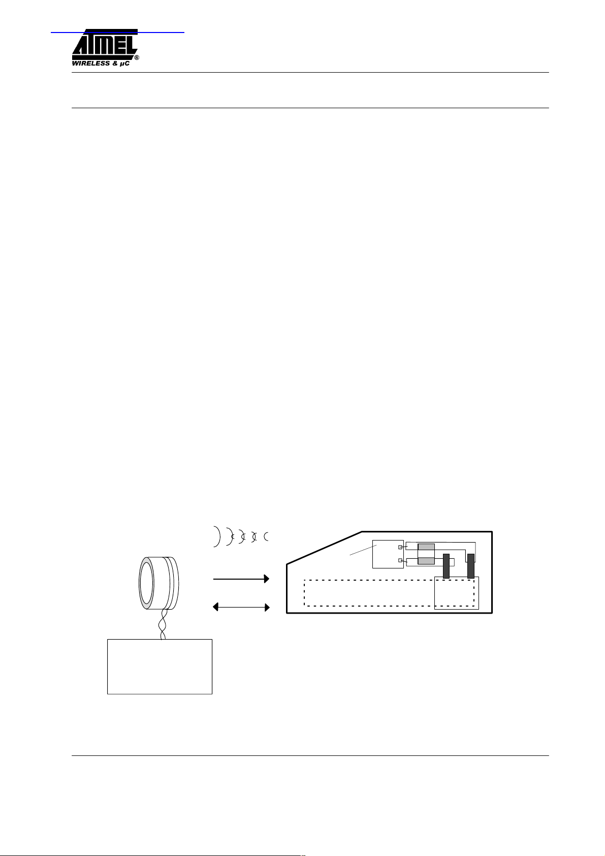
T ransponder TK5552
Transponder IC + coil + C in plastic cube
C
Transponder IC
Coil
Base station
*)
IDIC stands for IDentification Integrated Circuit and is a trademark of Atmel Wireless & Microcontrollers.
Rev. A5, 04-Oct-00 1 (20)
**)
**) for short distance U2270 B read/ write IC with MARC4 (see figure 12)
Figure 1. Transponder and base station
Preliminary Information
TK5552
Ordering Information
Extended Type Number Package Remarks
TK5552A–PP Plastic cube All kind of modulation; RF/16 and RF/32 *)
Default programmed: Manchester Modulation, RF/16,
MAXBLK = 1 to 31
*) see data sheet Transponder IC in the appendix
General
The transponder is the mobile part of the closed coupled
identification system (see figure 1), whereas the
read/ write base station is basing on the U2270B or other
solutions, and the read/ write transponder is basing on the
IDIC Transponder IC.
The transponder is a plastic-cube device consisting of
following parts:
D The transponder antenna, realized as tuned LC-circuit
D Read/ write IDIC (Transponder IC) with EEPROM
The Transponder Antenna
The antenna consists of a coil and a capacitor for tuning
the circuit to the nominal carrier frequency of 125 kHz.
The coil has a ferrite core for improving the distance of
read (uplink) and write (downlink) operations.
The Read/ Write IDIC
The read/ write IDIC Transponder IC is part of the transponder TK5552. The data are transmitted bidirectionally
between the base station and the transponder. The transponder receives power via a single coil from the RF signal
generated by the base station. The single coil is connected
to the chip and also serves as the IC’s bidirectional communication interface.
Data are transmitted by modulating the amplitude of the
RF signal. Reading (uplink) occurs by damping the coil
by an internal load. Writing (downlink) occurs by
interrupting the RF field in a specific way. The TK5552
transponder operates at a nominal frequency of 125 kHz.
There are different bit rates and encoding schemes.
The on-chip 1056-bit EEPROM (32 block, 33 bits each)
can be read (uplink) and written (downlink) blockwise
from the base station. The blocks can be protected against
overwriting by using lock bits. One block is reserved for
setting the operation modes of the IC.
See Transponder IC data sheet in the appendix for more
detailed information of IDIC .
2 (20)
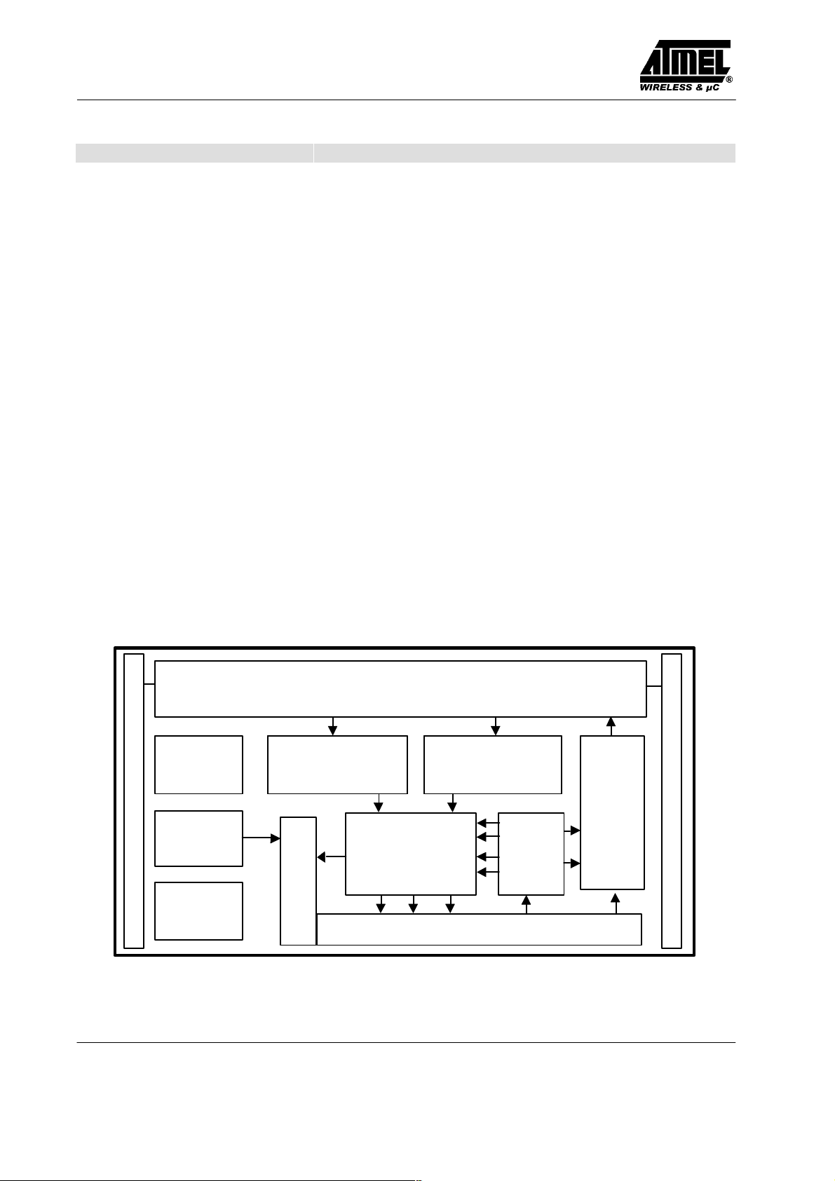
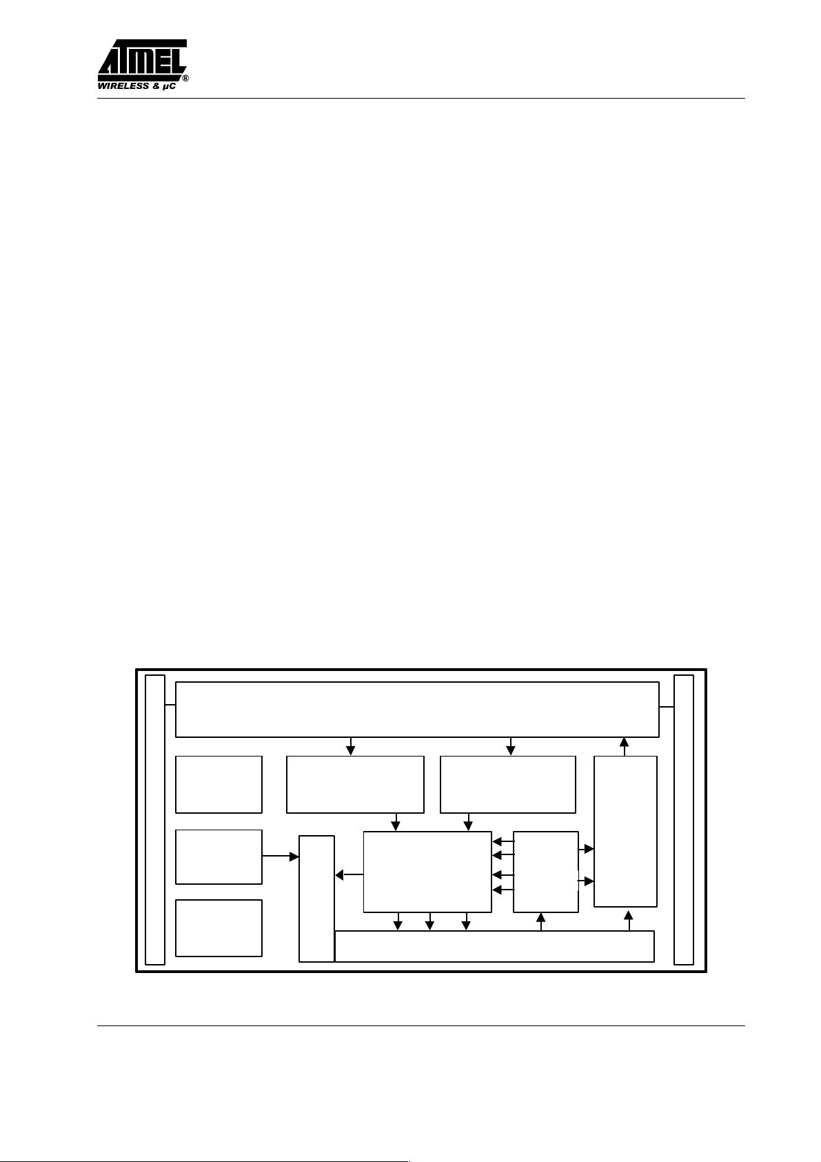
POR Bit decoderBit rate generator
Charge
Clock-A
pump
Start-up
delay
Analog front end
(rectifier, regulator, clock extractor, ESD protection)
Mode
Controller
Input register
Figure 2. Block diagram Transponder IC
EEPROM memory
register
Modulator
Rev. A5, 04-Oct-00
Clock-B
Preliminary Information

TK5552
Absolute Maximum Ratings
Parameters Symbol Value Unit
Operating temperature range T
Storage temperature range T
Maximum assembly temperature, t < 5 min. T
Magnetic field strength at 125 kHz H
amb
stg
ass
pp
Operating Characteristics Transponder
T
=
amb
25°C, f = 125 kHz Rf/32 and Manchester if not otherwise noted
Parameters Test Conditions Symbol Min. Typ. Max. Unit
Inductance L 4 mH
Resonance frequency LC circuit, HPP = 12 A/m f
Magnetic field strength (H)
Parameters Test Conditions Symbol Min. Typ. Max. Unit
Max. field strength where
tag does not modulate
Minimum field strength
Uplink/ downlink mode H
Programming mode H
Data retention EEPROM t
Programming cycles
EEPROM
Maximum field strength H
No influence to other tags
in the field
r
H
pp not
pp 25
pp 25
retention
pp max
119 125 131 kHz
100,000
–25 to +75 °C
–40 to +125 °C
170 °C
1000 A/m
4 A/m
12 A/m
18 A/m
10 Years
600 A/m
Rev. A5, 04-Oct-00 3 (20)
Preliminary Information
TK5552
4
3
2
1
0
–1
–2
–3
TK of resonance frequency ( % )
–4
–30–20 –100 1020304050607080
Temperature ( °C )
V2V1
V1 * V2
m +
V1 ) V2
Figure 3. Typical TK-range of resonance frequency
0.7
0.6
0.5
0.4
m ( 1 )
0.3
0.2
0.1
0.0
0 25 50 75 100 125
Quality factor (Q)
Hpp ( A/m)
Figure 4. Degree of modulation measurement
Degree of modulation (m)
Resonant frequency
127
126
125
124
123
122
121
120
35
30
25
20
Q ( 1 )
fres (kHz)
15
10
5
0
4 (20)
Figure 5. Typical behaviour of resonant frequency, degree of modulation and quality factor versus field strength
(by Rf/ 32, Manchester )
Rev. A5, 04-Oct-00
Preliminary Information
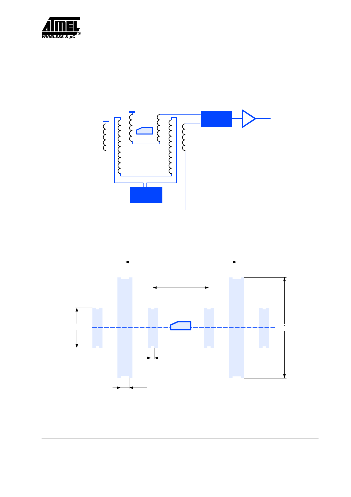
Measurement Assembly
All parameters are measured in a Helmholtz-arrangement, which generates a homogenous magnetic field (see
figure 6 and 7). A function generator drives the field
SENSING COILS ( IN PHASE )
TK5552
REFERENCE COIL
( IN PHASE )
FIELD GENERATING
COILS ( IN PHASE )
FUNCTION
GENERATOR
TK5552
generating coils, so the magnetic field can be varied in
frequency and field strength.
SUBTRACTOR
REFERENCE COIL ( IN PHASE )
AMPLIFIER
1:10
OUTPUT
VOLTAGE
24mm
REFERENCE COIL
Figure 6. Testing application
SENSING COIL
5mm
FIELD GENERATING COIL
TK5552
2mm
30mm
15mm
60mm
REFERENCE COIL
SENSING COIL
FIELD GENERATING COIL
Figure 7. Testing geometry
Rev. A5, 04-Oct-00 5 (20)
Preliminary Information

TK5552
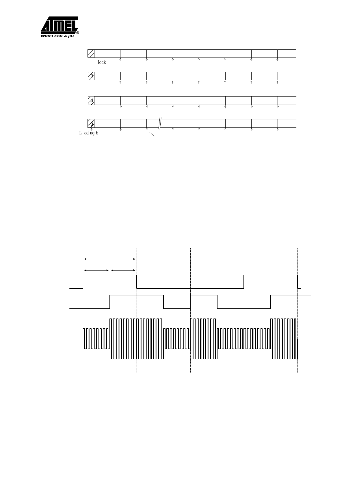
Downlink Operation
The write sequence (downlink mode) of the TK5552 is
shown below. Writing data into the transponder occurs by
interrupting the RF field with short gaps. After the start
gap the standard OP-code (11) is followed by the lockbit.
The next 32 bits contain the actual data. The last 5 bits
denote the destination block address. If the correct
number of bits have been received, the actual data is
programmed into the specified memory block.
RF field
Uplink mode Downlink mode
Standard OP–code
Start gap
Lock
bit
32 bit
01
Figure 8. Downlink protocol
Address bits (e.g. block 16)
01
0
0
> 64 clocks1 0
6 (20)
Figure 9. Explanation of the programming cycle
Rev. A5, 04-Oct-00
Preliminary Information

Downlink Data Decoding
The time elapsing between two detected gaps is used to
encode the information. As soon as a gap is detected, a
counter starts counting the number of field clock cycles
until the next gap will be detected. Depending on how
many field clocks elapse, the data is regarded as ’0’ or ’1’.
The required number of field clocks is shown in figure 10.
TK5552
A valid ’0’ is assumed if the number of counted clock
periods is between 16 and 32, for a valid ’1’ it is 48 or 64
respectively. If the data transmission was correct, programming is started and in case of success the written
block is cycling his data back to the base station until
POR.
Field clock cycles
Downlink data decoder
1 16324864
Fail 0 Fail 1 Downlink done
Figure 10. Downlink data decoding scheme
Behavior of the Real Device
The TK5552 detects a gap if the voltage across the coils
decreases below a threshold value of an internal MOS
transistor. Until then, the clock pulses are counted. The
number given for a valid ’0’ or ’1’ (see figure 10) refers
to the actual clock pulses counted by the device. However, there are always more clock pulses being counted
than were applied by the base station. The reason for this
is the fact that an RF field cannot be switched off immediately. The coil voltage decreases exponentially. So
although the RF field coming from the base station is
switched off, it takes some time until the voltage across
the coils reaches the threshold value of an internal MOS
transistor and the device detects the gap.
t
Coil
voltage
t
1
gap
t
0
01
1
12445
Referring to the following diagram (figure 11), this
means that the device uses the times t
0 internal
and t1
internal
The exact times for t0 and t1 are dependent on the application (e.g., field strength, etc.)
Typical time frames are:
t0 = 70 to 150 ms
t1 = 300 to 400 ms
t
= 180 to 400 ms
gap
Antennas with a high Q-factor require longer times for
t
and shorter time values for t0 and t1.
gap
t
Coil
t
1
gap
t
0
voltage
1 0
1
.
t
0 internal
12446
Gap detect
Ideal behavior
RF level reduces to zero immediately
Figure 11. Ideal and real behavior signals
Gap detect
t
1 internal
Real behavior
RF level decreases exponentially
Operating Distance
The maximum distance between the base station and the
TK5552 depends mainly on the base station, the coil
geometries and the modulation options chosen (see
U2270B Antenna Design Hints and the U2270B data
sheet). When using the Atmel Wireless & Microcontrollers U2270B demo board, the typical distances in the
range of 0 to 5 cm can be achieved. Maximum distance
Rev. A5, 04-Oct-00 7 (20)
values which are generally valid can not be given in this
data sheet. The exact measuring of the maximum distance
should be carried out with the TK5552 being integrated
into the specific application.
For longer distance used in industrial applications, please
use specific solutions like two or more reader coils.
Preliminary Information

TK5552
Application
V
31
470 kW
47 nF
1.5 nF
Power
Transponder IC
Transponder
22 mF
4.7 kW
1N4148
1.35 mH
TK5552
680 pF
1.2 nF
R
Data
V
V
Batt
DV
S
Input
COIL2
COIL1
DGND GND
EXTVS
U2270B
Standby
Read/write
circuit
f
Output
res
RF
MS
CFE
OE
Gain
+
100 nF
1
Ǹ
2p LC
110 kW
+
BP00
BP01
BP02
BP03
BP10
125 kHz
5 V
V
DD
M44C260
osc OUT
Micro-
controller
V
SS
osc IN
32 kHz
12456
Figure 12. Complete transponder system with the read/write base station IC U2270B
(only Manchester code, short distance)
8 (20)
Rev. A5, 04-Oct-00
Preliminary Information

Package Information
Dimensions in mm
TK5552
Rev. A5, 04-Oct-00 9 (20)
Preliminary Information

TK5552
Appendix: Transponder IC Read/Write Identification IC with 1 kbit Memory
Functional Description
The Transponder IC is a two-terminal, contactless
R/W-IDentification IC (IDIC
the 125 kHz (± 25 kHz) range. The IC uses the external
RF signal to generate its own power supply and internal
clock reference.
The IC contains a total of 1056 bits of EEPROM memory
grouped into 32 individually addressable data blocks.
Each block is made up of 32 bits of data plus an associated
lock bit for block write protection. Blocks 1 to 31 are
provided for user related data and block 0 for system
configuration.
)* for tag applications in
Features
D Low power, low voltage operation
D ESD protection: > 8 kV (HBM)
D Optimized for flipchip die attach processes
D Contactless power supply
D Contactless read/write data transmission
D Radio Frequency (RF): 100 kHz to 150 kHz
D 1056 bits of EEPROM memory
D 992 bits (31 x 32 bits) of user memory
Data is transmitted from the IC (uplink) using reflective
load (backscatter) modulation. This is achieved by
damping the external RF field by switching a resistive
load between the two terminals Clock–A/Clock–B as
shown in figure 14 (downlink). The IC receives and
decodes amplitude modulated data from the base station.
As soon as the tag including the Transponder IC is
exposed to an RF field and the field is strong enough to
derive enough energy to operate, the tag will respond by
continuously transmitting stored data (uplink mode). The
base station can at any time switch the tag into downlink
mode to write new user or configuration data. Generally,
the tag will automatically return to the default uplink
mode when the downlink transfer is complete, interrupted
or an error condition occurs.
D Auto-verify after EEPROM programming
D Block write protection for each block
D Configurable options include:
– Modulation type: PSK | Manchester
– Bit rate [bit/s]: RF/16 | RF/32
– Number of readable blocks
– Modulation defeat
D Defined start of data transmission
Power
Power
Base station
Base station
Figure Appendix 1. Transponder system example using Transponder IC
* IDICstands for IDentification Integrated Circuit and is a trademark of Atmel Wireless & Microcontrollers
10 (20)
Data
downlink
Data
uplink
– POR start-up delay: ≈ 1 ms | ≈ 65 ms
Transponder
Transponder
Memory
Memory
Controller
Coil interface
Analog frontend
Controller
Transponder IC
Rev. A5, 04-Oct-00
Preliminary Information
Functional Modules
TK5552
Analog Front End (AFE)
The analog front end (AFE) includes all circuits which are
directly connected to the coil. It generates the IC’s power
supply and handles the bidirectional data communication
with the basestation. It consists of the following blocks:
D Rectifier to generate a DC supply voltage from the AC
coil voltage.
D ESD protection
D Clock extractor
D Switchable load between Clock-A/ Clock-B for data
transmission from the IC to the reader electronics
(uplink mode).
D Field gap detector for data transmission from the base
station to the IC (downlink mode).
Controller
The control logic is responsible for the following:
D Initializing and refresh configuration register from
EEPROM block 0.
D Controlling read and write memory accesses.
D Handling data transmission and opcode decoding.
D Error detection and error handling.
Clock Extraction
The clock extraction circuit generates the internal clock
source out of the external RF signal.
Data Rate Generator
The data rate in uplink mode can be selected to operate
at either RF/16 (nominally 7.81 kHz, default) or RF/32
(nominally 3.91 kHz).
Bit Decoder
This function block decodes the field gaps and verifies the
validity of the incoming data stream.
Charge Pump
This circuit generates the high voltage required for programming the EEPROM.
Power-On Reset (POR)
This circuit delays the IC’s functionality until an acceptable voltage threshold has been reached.
Mode Register
This register holds the configuration data bits stored in
EEPROM block 0. It is refreshed at the start of every
block read operation.
Modulator
The modulator encodes the serial data stream shifted out
of the selected EEPROM data block and controls the
damping circuit in the AFE. The Transponder IC frontend
supports PSK and Manchester encoding.
Analog front end
(rectifier, regulator, clock extractor, ESD protection)
POR Bit decoderBit rate generator
Charge
Clock-A
pump
Controller
Mode
register
Modulator
Clock-B
Start-up
delay
Rev. A5, 04-Oct-00 11 (20)
Input register
Figure Appendix 2. Functional block diagram
EEPROM memory
Preliminary Information

TK5552
Operating the Transponder IC
Damping on
Damping off
Loading block 0 (114 FC [ 1 ms),
start-up delay inactive
Power-on reset
Figure Appendix 3. Voltage at Clock-A/ Clock-B after power on
General
The basic functions of the Transponder IC are to supply
the IC from the RF field, read data out of the EEPROM
and shift them to the modulator, receive data and program
these data bits into the EEPROM. An error detecting circuit prevents the EEPROM from being written with
wrong data.
Power Supply
The IC is supplied via a tuned LC circuit which is connected to the Clock-A/Clock-B pads. The incoming RF
induces a current in the coil. The on-chip rectifier generates the DC supply voltage. Overvoltage protection
prevents the IC from damage due to high field strengths.
Depending on the coil, the open-circuit voltage across the
LC circuit can reach more than 100 V.
Initialization
The occurrence of a RF field triggers a power–on reset
pulse, ensuring a defined start-up. The Power-On-Reset
circuit (POR) remains active until an adequate voltage
threshold has been reached. This in turn triggers the default start-up delay sequence. During this period of 114
field clock cycles (FC) the Transponder IC is initialized
with the configuration data stored in EEPROM block 0.
This is followed by an additional delay time which is defined by the ”Start-up Delay” bit.
Read data with selected
modulation and bitrate
Any field gap occuring during initialization will restart
the complete sequence.
T
= (114 + 8,192*delay bit)/125 kHz ≈ 65 ms
INIT
After this initialization time the Transponder IC enters
uplink mode and modulation starts automatically using
the parameters defined in the configuration block.
Uplink Operation
All transmissions from the IC to the base station utilizes
amplitude modulation (ASK) of the RF carrier. This takes
place by switching a resistive load between the coil pads
(Clock-A and Clock-B) which in turn modulates the RF
field generated by the base station (reflective backscatter
modulation).
MaxBlock
Data from the memory is serially transmitted, starting
with block 1, bit 1, up to the last block (MAXBLK), bit
32. The last block which will be transmitted is defined by
the mode parameter field MAXBLK is stored in EEPROM block 0. When the MAXBLK address has been
reached, data transmission restarts with block 1.
The user defines the cyclic datastream by setting the
MAXBLK between 0 and 31 (representing each of the 32
data blocks). If set to 1, only block 1 is transmitted. If set
to 31, blocks 1 to 31 will be sequentially transmitted. If
set to 0, only the contents of the configuration block (normally not accessible) will be transmitted (see figure 4).
If the ”Start-up Delay” bit is set the Transponder IC remains inactive until 8192 RF clock cycles have occured.
If this option is deactivated, no delay is observed after the
configuration period of 114 RF clock cycles (≈ 1 ms).
12 (20)
Preliminary Information
On the other hand it is also possible to access a single data
block selectively, independant of the MAXBLK value,
with the direct access command (Opcode ‘11’). The thus
addressed data block is transmitted repeatedly.
Rev. A5, 04-Oct-00
TK5552
0
MAXBLK = 0
MAXBLK = 1
MAXBLK = 2
Loading block 0
Loading block 0
Loading block 0
Loading block 0
(not transmitted)
Block 0 Block 0 Block 0 Block 0 Block 0
0
Block 1 Block 1 Block 1 Block 1 Block 1
0
Block 1 Block 2 Block 1 Block 2 Block 1
Block 1 Block 2 Block 30 Block 31MAXBLK = 31
0
Refreshing configuration register
Figure Appendix 4. Datastream pattern depending on MAXBLK
Data Encoding
Everytime when entering uplink mode, the data stream is
preceeded by a single start bit (always ‘0’). Then the data
stream continues with block 1, bit 1, and continues
through MAXBLK, bit 32. This data stream pattern
cycles continuously.
The modulator is configurable for
Block 0
Block 1
Block 2
Block 1
Block 0
Block 1
Block 1
Block 2
....
....
....
....
16546
D MANCHESTER
Manchester encoded data represent a logical ‘1’ with a
rising edge and a logical ‘0’ with a falling edge.
D PSK using sub-carrier frequency RF/2
The PSK modulator changes phase with each change of
data. The first phase shift represents a data change from
‘0’ ––> ‘1’.
Datastream
Manchester
encoded
RF-field
Data rate =
16 Field Clocks (FC)
21
1001
8 FC8 FC
9
Figure Appendix 5. Example of Manchester encoding with data rate RF/16
16818 18 9 16
16 1 8916
16552
Rev. A5, 04-Oct-00 13 (20)
Preliminary Information

TK5552
Data rate =
16 Field Clocks (FC)
Datastream
Inverted
modulator
signal
subcarrier RF/2
21891618 1618 161 8
RF-field
1001
8 FC8 FC
Figure Appendix 6. Example of PSK encoding with data rate RF/16
Downlink Operation
Data is transmitted from the base station by amplitude
modulation of the field (m = 1) using a series of so called
gaps. With the exception of the initial synchronisation
gap (start gap), all field gaps have the same duration, the
logical data being encoded in the length of the unmodulated phases (see figure A 7)
A valid data stream is always preceeded by a start gap
which is approximately twice as long as a normal field
gap. Detection of this first gap causes the Transponder IC
to switch immediately into the downlink mode where it
can receive and decode the following data stream. This
stream consists of two opcode bits, followed by (0 or 33)
data bits (including the lock bit) and finally (0, 3 or 5) address bits. In downlink mode the transponder damping is
permanently enabled. This loads the resonant transponder
coil circuit so that it comes quickly to rest when field gaps
occur – thus allowing fast gap detection.
Read mode Receive mode
RF
Damping ON
Damping OFF
Figure Appendix 7. Entering the downlink mode
Field gap + data ’0‘
Field gap + data ’1‘
Start gap + data ’0‘
16559
A start gap will be accepted at any time after start–up initialization has been finished (RF field ON plus ≈ 1 ms,
startup delay inactive) and the IC is not in downlink operation.
Downlink Data Coding
The duration of a field gap is typically between 80 and
250 µs. After the start gap the data bits are transmitted by
the base station whereby each bit is separated by a field
gap. The bit decoder interprets 16 to 32 internal field
clocks as a logical ‘0’ and 48 to 64 internal field clocks
as a logical ‘1’ (see figure A 8). Therefore the time between two gaps is typically 24 field clocks for a ‘0’ and
56 field clocks for a ‘1’.
Whenever the bit decoder detects more than 64 field
clocks, the Transponder IC will abort the downlink mode.
The incoming data stream is checked continuously and
should an error be detected the corresponding error handling is initiated.
The control logic initiates an EEPROM programming
cycle if the correct number of bits had been received (see
figure A 9).
14 (20)
Rev. A5, 04-Oct-00
Preliminary Information

TK5552
Uplink mode
start gap detected ?
YES
Downlink mode
count field clocks FC
FC count > 64 ?
NO
gap detected ?
YES
16 <= FC <= 32 ?
NO
48 <= FC <= 64 ?
NO
YES
Data stream check
NO
YES
’0’ into shift register
YES
’1’ into shift register
Data stream check
OPCODE ’11’ ?
NO
OPCODE ’10 ’ ?
YES
bitcount = 38 ? bitcount = 40 ?
NO
enter error handler
–> ”Frame error”
YES
NO
Execute command
’00’ or ’01’
YES YES
Programming
NO
bitcount = 7 ?
NO
YES
NO
enter error handler
–> ”Bit Error”
Uplink mode
Figure Appendix 8. Operation of bit decoder – data stream
decoder
Opcode definitions
The first two bits of the data stream are decoded by the
controller as the opcode bits (see figure A 10):
‘11’: Opcode for a 5-bit address data stream
D To initiate a standard block write cycle the 2 opcode
bits are followed by the lock bit, the 32 data bits and
the 5-bit block address (40 bits total).
D The direct access command consists of the opcode
‘11’ followed by the 5-bit block address and is a read–
only command (7 bits total).
enter uplink mode
–>block 1...MAXBLK
Direct access mode
enter uplink mode
–> selected block
Figure Appendix 9. Data stream checking
‘10’: Opcode for a 3-bit address data stream
D e5550 receive mode compatible
To initiate a block write cycle, the opcode ‘10’ is followed by the lock bit, the 32 data bits and the 3-bit
block address (38 bits total).
‘01’: reserved for production test commands.
‘00’: Opcode for an internal reset command.
Rev. A5, 04-Oct-00 15 (20)
Preliminary Information

TK5552
Standard block write
Short block write
Direct access command
Reset command
OP
11
OP
10
L 321
OP
11
40
Addr
OP
00
Figure Appendix 10. Transponder IC opcode format definition
Data bitsL 321
Data bits
Addr20
4
Addr
0
enter error handler
–> ”Verification error”
PROGRAMMING
turn off transponder
damping
addressed block
locked ?
NO
generate high
programming voltage
erase block
NO
erase successful ?
YES
program ’1’s
NO
programming ’1’s
successful ?
YES
enter uplink mode
–> read selected block
YES
Programming
If the bit decoder and controller detect a valid data stream,
the Transponder IC will start an erase and programming
cycle if a data write command was decoded (see figure
A 11).
During the erase and programming cycle downlink damping is turned off. The programming cycle includes a data
verification read to check the integrity of the data. After
EEPROM programming and verification has been finished successfully, the Transponder IC enters uplink
mode transmitting the block just programmed.
The typical programming time is ≈ 18 ms.
Error Handling
Several error conditions are detected by the Transponder
IC to ensure that only valid information is programmed
into the EEPROM.
Errors During EEPROM Programming
There are two error types which will lead to different actions.
D Verification error
If one of the data verification cycles fails, the
Transponder IC will inhibit modulation and not return
to the uplink mode. This ”modulation defeat” state is
terminated by re-entering the downlink mode with a
start gap.
D Block write protection
enter
”Modulation Defeat”
Figure Appendix 11. Programming cycle flow chart
16 (20)
Preliminary Information
16551
If the lock bit of the addressed block is set, programming is disabled. In this case, the programming cycle
is not initiated and the Transponder IC reverts to
uplink mode, transmitting the currently addressed
(and unmodified) block continuously.
Rev. A5, 04-Oct-00

TK5552
Errors During Data Transmission
The following errors are detected by the decoder:
D Bit error
Wrong number of field clocks between two gaps (i.e.
not a valid ‘0’ or ‘1’ pulse stream).
D Frame error
The number of data bits received is incorrect:
– valid bit count for 3-bit address write is 38 bits
– valid bit count for 5-bit address write is 40 bits or
– 7 bits for a direct access command.
If any of these conditions is detected, the Transponder IC
enters uplink mode starting with block 1.
EEPROM Memory Organisation
The memory array of the Transponder IC consists of
1,056 bits of EEPROM, arranged in 32 individually addressable blocks of 33 bits each, consisting of one lock bit
and 32 data bits. All 33 bits, including the lock bit, are
programmed simultaneously.
The programming voltage is generated on-chip.
Lock bit
Each block has an associated write lock bit with which the
entire block can be protected. By default all lock bits L
are reset (‘0’).
Note: Once set, the lock bit – and the content of the asso-
ciated block – cannot be altered.
1320
L
L
L
L
L
L
Not transmitted
Configuration data block
User data bits
User data bits
User data bits
User data bits
User data bits
33 bits total (incl. one lock bit)
Figure Appendix 12. Memory map
Block 0
Block 1
Block 2
Block 29
Block 30
Block 31
16549
Configuration Data Block
This data block contains 9 configuration bits.
The remaining bits of block 0 are reserved for future en-
hancements and should be set to ‘0’.
D Start-up Delay bit (SD, default: NO delay)
When set, an additional delay time of 64 ms is added
after any internal reset.
D Data Rate bit (DR, default: RF/16)
Selects data rate of RF/16 or RF/32.
D Modulation Select bit (MS, default is PSK)
Selects type of data encoding which is either
MANCHESTER or PSK.
D Modulation Defeat bit (MD, default is OFF)
When set (to ‘1’) the modulation output is deactivated, hence no data will be transmitted. The
”modulation defeat” state does not impact the transponder damping function.
Memory Map
The configuration data of the Transponder IC is stored in
block 0 of the EEPROM.
The remaining thirty-one data blocks (1 .. 31) each consist
of one lock bit and 32 user data bits.
Rev. A5, 04-Oct-00 17 (20)
D MAXBLK address bits (MAXBLK, default is 31)
This 5-bit block address is used to define the upper
limit of cyclic block reads.
Note: The configuration is changed by re-programming
block 0 as long as the corresponding lock bit is not set.
The default settings can be lost due to the die cut.
Preliminary Information

TK5552
Transponder IC Configuration Block 0
L 1 2 3 456789 10 11 12 13 14 15 16 17 18 19 20 21 22 23 24 25 26 27 28 29 30 31 32
0 0 0 0 0 0 0 0 0 0 0 0 0 0 0 0 0 0 0 0 0 0 0
reserved, to be ’0‘
Lockbit
Data rate DR
Start-up delay SD
0 = Unlocked 0 = PSK
1 = Locked 1 = MANCHESTER
NO delay =
Delay of 8,192 field clocks =0101
= RF/16
= RF/32
MAXBLOCK
00000 = Block 0
00001 = Block 1
00010 = Block 1...2
00011 = Block 1...3
MD
11111 = Block 1...31
Modul. select MS
Modulation Defeat
0 = Normal function
1 = Modulation off
reserved
Figure Appendix 13. Transponder IC configuration block 0 bit mapping
1.5k
Clock-A
Clock-B
Figure Appendix 14. Simplified damping circuit
1.5k
~ 2 V
~ 2 V
Mod
16580
18 (20)
Rev. A5, 04-Oct-00
Preliminary Information

TK5552
Absolute Maximum Ratings
Parameters Symbol Value Unit
Maximum DC current into Clock-A/Clock-B Icoil 10 mA
Maximum AC current into Clock-A/Clock-B,
f = 125 kHz
Power dissipation (dice)
Electrostatic discharge voltage according to MIL-Stan-
dard 883D method 3015 (HBM)
Operation ambient temperature range Tamb –25 to +75 °C
Storage temperature range
Maximum assembly temperature for less than 5 min
Notes: 1) Free–air condition, time of application: 1s
2) Data retention reduced
3) Assembly temperature of 150°C for less than 5 minutes does not affect the data retention
Stresses above those listed under ”Absolute Maximum Ratings” may cause permanent damage to the device.
1)
2)
3)
Icoil PP 20 mA
Ptot 100 mW
Vmax 8000 V
Tstg –40 to +125 °C
Tsld +150 °C
Operating Charateristics
T
= 25°C; fRF = 125 kHz reference terminal is VSS
amb
Parameters Test Conditions / Pins Symbol Min. Typ. Max. Unit
RF frequency range fRF 100 125 150 kHz
Supply current Uplink & downlink mode –
full temperature range
Programming – full tem-
perature range
Clamp voltage 10 mA current into Clock-
A/B
Programming time Per block tP 18 ms
Startup time 2) t startup 1 65 ms
Data retention 1) t retention 10 Years
Programming cycles 1) ncycles 100,000
Clock-A/B voltage Uplink & downlink mode VclockPP 6 V
Clock-A/B voltage Programming, RF field w/o
damping
Damping resistor Each at Clock-A and
Clock-B
IDD 5 7.5 µA
IDD 14 28 µA
Vclamp 7 11 V
VclockPP 12 V
RD 1.5 kΩ
Note: 1) Since EEPROM performance is influenced by assembly and packaging, Atmel Wireless & Microcontrollers
confirms the parameters for DOW (= tested dice on wafer) and ICs assembled in standard package.
2) Depends on start-up delay bit in configuration register
Rev. A5, 04-Oct-00 19 (20)
Preliminary Information

TK5552
Ozone Depleting Substances Policy Statement
It is the policy of Atmel Germany GmbH to
1. Meet all present and future national and international statutory requirements.
2. Regularly and continuously improve the performance of our products, processes, distribution and operating systems
with respect to their impact on the health and safety of our employees and the public, as well as their impact on
the environment.
It is particular concern to control or eliminate releases of those substances into the atmosphere which are known as
ozone depleting substances (ODSs).
The Montreal Protocol (1987) and its London Amendments (1990) intend to severely restrict the use of ODSs and forbid
their use within the next ten years. Various national and international initiatives are pressing for an earlier ban on these
substances.
Atmel Germany GmbH has been able to use its policy of continuous improvements to eliminate the use of ODSs listed
in the following documents.
1. Annex A, B and list of transitional substances of the Montreal Protocol and the London Amendments respectively
2. Class I and II ozone depleting substances in the Clean Air Act Amendments of 1990 by the Environmental
Protection Agency (EPA) in the USA
3. Council Decision 88/540/EEC and 91/690/EEC Annex A, B and C (transitional substances) respectively.
Atmel Germany GmbH can certify that our semiconductors are not manufactured with ozone depleting substances
and do not contain such substances.
6.
We reserve the right to make changes to improve technical design and may do so without further notice.
Parameters can vary in different applications. All operating parameters must be validated for each customer
application by the customer. Should the buyer use Atmel Wireless & Microcontrollers products for any unintended
or unauthorized application, the buyer shall indemnify Atmel Wireless & Microcontrollers against all claims,
costs, damages, and expenses, arising out of, directly or indirectly, any claim of personal damage, injury or death
associated with such unintended or unauthorized use.
20 (20)
Data sheets can also be retrieved from the Internet: http://www.atmel–wm.com
Atmel Germany GmbH, P.O.B. 3535, D-74025 Heilbronn, Germany
Telephone: 49 (0)7131 67 2594, Fax number: 49 (0)7131 67 2423
Rev. A5, 04-Oct-00
Preliminary Information
 Loading...