

Page 1

Features
• 80C51 Core Architecture
• 256 Bytes of On-chip RAM
• 1K Bytes of On-chip XRAM
• 32K Bytes of On-chip Flash Memory
– Data Retention: 10 Years at 85°C
Erase/Write Cycle: 100K
• Boot Code Section with Independent Lock Bits
• 2K Bytes of On-chip Flash for Bootloader
• In-System Programming by On-Chip Boot Program (CAN, UART) and IAP Capability
• 2K Bytes of On-chip EEPROM
Erase/Write Cycle: 100K
• 14-sources 4-level Interrupts
• Three 16-bit Timers/Coun ter s
• Full Duplex UART Compatible 80C51
• Maximum Crystal Frequency 40 MHz, in X2 Mode, 20 MHz (CPU Core, 20 MHz)
• Five Ports: 32 + 2 Digital I/O Lines
• Five-channel 16-bit PCA with:
– PWM (8-bit)
– High-speed Output
– Timer and Edge Capture
• Double Data Pointer
• 21-bit Watchdog Timer (7 Programmable Bits)
• A 10-bit Resolution Analog to Digital Converter (ADC) with 8 Multiplexed Inputs
• Full CAN Controller:
– Fully Compliant with CAN Rev2.0A and 2.0B
– Optimized Structure for Communication Management (Via SFR)
– 15 Independent Message Objects:
Each Message Object Programmable on Transmission or Reception
Individual Tag and Mask Filters up to 29-bit Identifier/Channel
8-byte Cyclic Data Register (FIFO)/Message Object
16-bit Status and Control Register/Message Object
16-bit Time-Stamping Registe r/Message Object
CAN Specification 2.0 Part A or 2.0 Part B Programmable for Each Message
Object
Access to Message Object Control and Da ta Registers Via SFR
Programmable Reception Buffer Length Up To 15 Message Objects
Priority Management of Reception of Hits on Several Message Objects at the
Same Time (Basic CAN Feature)
Priority Management for Transmission
Message Object Overrun Interrupt
– Supports:
Time Triggered Communication
Autobaud and Listening Mode
Programmable Automatic Reply Mode
– 1-Mbit/s Maximum Transfer Rate at 8 MHz
– Readable Error Counters
– Programmable Link to On-chip Timer for Time Stamping and Network
Synchronization
– Independent Baud Rate Prescaler
– Data, Remote, Error and Overload Frame Handling
• On-chip Emulation Logic (Enhanced Hook System)
• Power Saving Modes:
–Idle Mode
– Power-down Mode
(1)
Crystal Frequency in X2 Mode
Enhanced 8-bit
Microcontroller
with CAN
Controller and
Flash Memory
T89C51CC01
AT89C51CC01
1. At BRP = 1 sam pling point will be fixed.
Rev. 4129L–CAN–08/05
1
Page 2
A/T89C51CC01
• Power Supply: 3V to 5.5V
• Temperature Range: Industrial (-40° to +85°C)
• Packages: VQFP44, PLCC44, CA-BGA64
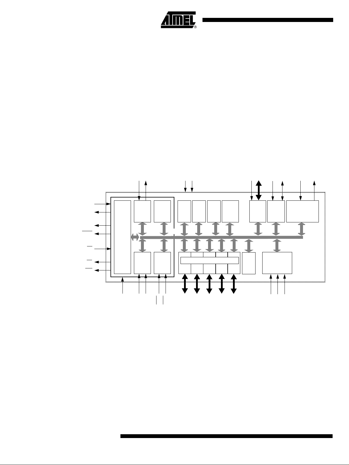
Description The T89C51CC01 is the first member of the CANary
dedicated to CAN network applications.
In X2 mode a maximum external clock rate of 20 MHz reaches a 300 ns cycle time.
Besides the full CAN co ntroller T89C51CC 01 provides 32K Byte s of Flash memory
including In-System-Programming (ISP), 2K Bytes Boot Flash Memory, 2K Bytes
EEPROM and 1.2-Kbyte RAM.
Special attention is paid to the reduction of the electro-magnetic emission of
T89C51CC01.
Block Diagram
Vss
IB-bus
Flash
32kx
8
Vcc
Boot
loader
2kx8
EE
PROM
2kx8
XRAM
1kx8
XTAL1
XTAL2
ALE
PSEN
CPU
RxD
UART
TxD
C51
CORE
RAM
256x8
TM
family of 8-bit microcontrollers
TxDC
ECI
PCA
PCA
T2EX
Timer 2
RxDC
T2
CAN
CONTROLLER
EA
RD
WR
Notes: 1. 8 analog Inputs/8 Digital I/O
2. 2-Bit I/O Port
Timer 0
Timer 1
T0
RESET
T1
INT
Ctrl
INT0
Parallel I/O Ports and Ext. Bus
Port 0P0Port 1
INT1
Port 2
P1(1)
P2
Port 3
P3
Port 4
P4(2)
Watch
Dog
10 bit
ADC
VAREF
VAVCC
VAGND
2
4129L–CAN–08/05
Page 3
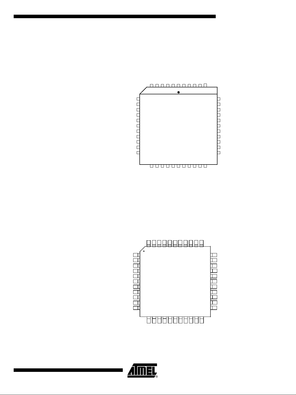
Pin Configuration
P1.4/AN4/CEX1
P1.5/AN5/CEX2
P1.6/AN6/CEX3
P1.7/AN7/CEX4
EA
P3.0/RxD
P3.1/TxD
P3.2/INT0
P3.3/INT1
P3.4/T0
P3.5/T1
7
8
9
10
11
12
13
14
15
16
17
P1.3/AN3/CEX0
P1.2/AN2/ECI
P1.1/AN1/T2EX
P1.0/AN 0/T2
65432
PLCC44
VAREF
VAGND
RESET
1
4443424140
A/T89C51CC01
VSS
VCC
XTAL1
XTAL2
39
ALE
38
PSEN
37
P0.7/AD7
36
P0.6/AD6
35
P0.5/AD5
34
P0.4/AD4
33
P0.3/AD3
32
P0.2/AD2
31
P0.1/AD1
30
P0.0/AD0
29
P2.0/A8
P1.4/AN4/CEX1
P1.5/AN5/CEX2
P1.6/AN6/CEX3
P1.7/AN7/CEX4
EA
P3.0/RxD
P3.1/TxD
P3.2/INT0
P3.3/INT1
P3.4/T0
P3.5/T1
1819202122232425262728
P3.7/RD
1
2
3
4
5
6
7
8
9
10
11
P1.3/AN3/CEX0
P3.6/WR
P1.2/AN2/ECI
43 42 41 40 3944
P4.1/RxDC
P4.0/ TxDC
P1.1/AN1/T2EX
P1.0/AN 0/T2
VAREF
VQFP44
P2.7/A15
P2.6/A14
P2.5/A13
VAGND
RESET
VSS
38 37 36 35 34
12 13 17161514 201918 21 22
P2.4/A12
P2.1/A9
P2.3/A11
P2.2/A10
VCC
XTAL1
XTAL2
33
ALE
32
PSEN
31
P0.7/AD7
30
P0.6/AD6
29
P0.5/AD5
28
P0.4 /AD4
27
P0.3 /AD3
26
P0.2 /AD2
25
P0.1 /AD1
24
P0.0 /AD0
23
P2.0/A8
4129L–CAN–08/05
P3.7/RD
P3.6/WR
P2.7/A15
P2.6/A14
P2.5/A13
P4.0/TxDC
P4.1/RxDC
P2.4/A12
P2.1/A9
P2.3/A11
P2.2/A10
3
Page 4

A/T89C51CC01
CA-BGA64 To p View
21 345678
A
B
C
D
E
F
G
H
EA
P3.0
P3.2
P3.4
P3.6
P1.2/AN2P1.4/AN4 P1.0/AN0
P1.3/AN3P1.5/AN5
P1.6/AN6
NC
P3.1
P3.3 NC
P3.5
P1.1/AN1
NC
NC NC RESET
NC
P4.0
P2.7P3.7
VAGND
VAREF VDD
NCP1.7/AN7
NC
NC
P4.1
P2.6
VSS
VDD
NC
NC
NC
P2.4
P2.5 P2.3 P2.1 P2.0
VSS XTAL1
NC P0.6
NC P0.2 P0.4
NC P0.1 P0.3
P2.2 NC P0.0
NC ALE
PSENNC
XTAL2
P0.7
P0.5
4
4129L–CAN–08/05
Page 5

Table 1. Pin Description
Pin Name Type Description
VSS GND Circuit ground
VCC Supply Voltage
VAREF Reference Voltage for ADC (input)
VAGND Reference Ground for ADC (internally connected to VSS)
P0.0:7 I/O Port 0:
Is an 8-bit open drain bi-directional I/O port. Port 0 pins that have 1’s written to them float, and in this state can be used as
high-impedance inputs. Port 0 is also the multiplexed low-order address and data bus during accesses to external Program
and Data Memory. In this application it uses strong internal pull-ups when emitting 1’s.
Port 0 also outputs the code Bytes during program validation. External pull-ups are required during program verification.
A/T89C51CC01
P1.0:7 I/O Port 1:
Is an 8-bit bi-directional I/O port with internal pull-ups. Port 1 pins can be used for digital input/output or as analog inputs for
the Analog Digital Converter (ADC). Port 1 pins that have 1’s written to them are pulled high by the internal pull-up transistors
and can be used as inputs in this state. As inputs, Port 1 pins that are being pulled low externally will be the source of current
(I
, see section "Electrical Characteristic") because of the internal pull-ups. Port 1 pins are assigned to be used as analog
IL
inputs via the ADCCF register (in this case the internal pull-ups are disconnected).
As a secondary digital function, port 1 contains the Timer 2 external trigger and clock input; the PCA external clock input and
the PCA module I/O.
P1.0/AN0/T2
Analog input channel 0,
External clock input for Timer/counter2.
P1.1/AN1/T2EX
Analog input channel 1,
Trigger input for Timer/counter2.
P1.2/AN2/ECI
Analog input channel 2,
PCA external clock input.
P1.3/AN3/CEX0
Analog input channel 3,
PCA module 0 Entry of input/PWM output.
P1.4/AN4/CEX1
Analog input channel 4,
PCA module 1 Entry of input/PWM output.
P1.5/AN5/CEX2
Analog input channel 5,
PCA module 2 Entry of input/PWM output.
P1.6/AN6/CEX3
Analog input channel 6,
PCA module 3 Entry of input/PWM output.
P1.7/AN7/CEX4
Analog input channel 7,
PCA module 4 Entry ot input/PWM output.
Port 1 receives the low-order address byte during EPROM programming and program verification.
It can drive CMOS inputs without external pull-ups.
P2.0:7 I/O Port 2:
4129L–CAN–08/05
Is an 8-bit bi-directional I/O port with internal pull-ups. Port 2 pins that have 1’s written to them are pulled high by the internal
pull-ups and can be used as inputs in this state. As inputs, Port 2 pins that are being pulled low externally will be a source of
current (I
during accesses to the external Program Memory and during accesses to external Data Memory that uses 16-bit addresses
(MOVX @DPTR). In this application, it uses strong internal pull-ups when emitting 1’s. During accesses to external Data
Memory that use 8 bit addresses (MOVX @Ri), Port 2 transmits the contents of the P2 special function register.
It also receives high-order addresses and control signals during program validation.
It can drive CMOS inputs without external pull-ups.
, see section "Electrical Characteristic") because of the internal pull-ups. Port 2 emits the high-order address byte
IL
5
Page 6

A/T89C51CC01
Table 1. Pin Description (Continued)
Pin Name Type Description
P3.0:7 I/O Port 3:
Is an 8-bit bi-directional I/O port with internal pull-ups. Port 3 pins that have 1’s written to them are pulled high by the internal
pull-up transistors and can be used as inputs in this state. As inputs, Port 3 pins that are being pulled low externally will be a
source of current (I
The output latch corresponding to a secondary function must be programmed to one for that function to operate (except for
TxD and WR
P3.0/RxD:
Receiver data input (asynchronous) or data input/output (synchronous) of the serial interface
P3.1/TxD:
Transmitter data output (asynchronous) or clock output (synchronous) of the serial interface
P3.2/INT0
External interrupt 0 input/timer 0 gate control input
P3.3/INT1
External interrupt 1 input/timer 1 gate control input
P3.4/T0:
Timer 0 counter input
P3.5/T1:
Timer 1 counter input
P3.6/WR
External Data Memory write strobe; latches the data byte from port 0 into the external data memory
P3.7/RD
External Data Memory read strobe; Enables the external data memory.
It can drive CMOS inputs without external pull-ups.
). The secondary functions are assigned to the pins of port 3 as follows:
:
:
:
:
, see section "Electrical Characteristic") because of the internal pull-ups.
IL
P4.0:1 I/O Port 4:
Is an 2-bit bi-directional I/O port with internal pull-ups. Port 4 pins that have 1’s written to them are pulled high by the internal
pull-ups and can be used as inputs in this state. As inputs, Port 4 pins that are being pulled low externally will be a source of
current (IIL, on the datasheet) because of the internal pull-up transistor.
The output latch corresponding to a secondary function RxDC must be programmed to one for that function to operate. The
secondary functions are assigned to the two pins of port 4 as follows:
P4.0/TxDC:
Transmitter output of CAN controller
P4.1/RxDC:
Receiver input of CAN controller.
It can drive CMOS inputs without external pull-ups.
6
4129L–CAN–08/05
Page 7

Table 1. Pin Description (Continued)
Pin Name Type Description
Reset:
RESET I/O
ALE O
PSEN O
EA I
XTAL1 I
A high level on this pin during two machine cycles while the oscillator is running resets the device. An internal pull-down
resistor to VSS permits power-on reset using only an external capacitor to VCC.
ALE:
An Address Latch Enable output for latching the low byte of the address during accesses to the external memory. The ALE is
activated every 1/6 oscillator periods (1/3 in X2 mode) except during an external data memory access. When instructions are
executed from an internal Flash (EA
PSEN
:
The Program Store Enable output is a control signal that enables the external program memory of the bus during external
fetch operations. It is activated twice each machine cycle during fetches from the external program memory. However, when
executing from of the external program memory two activations of PSEN are skipped during each access to the external Data
memory. The PSEN is not activated for internal fetches.
:
EA
When External Access is held at the high level, instructions are fetched from the internal Flash when the program counter is
less then 8000H. When held at the low level,T89C51CC01 fetches all instructions from the external program memory
XTAL1:
Input of the inverting oscillator amplifier and input of the internal clock generator circuits.
To drive the device from an external clock source, XTAL1 should be driven, while XTAL2 is left unconnected. To operate
above a frequency of 16 MHz, a duty cycle of 50% should be maintained.
A/T89C51CC01
= 1), ALE generation can be disabled by the software.
.
XTAL2 O
XTAL2:
Output from the inverting oscillator amplifier.
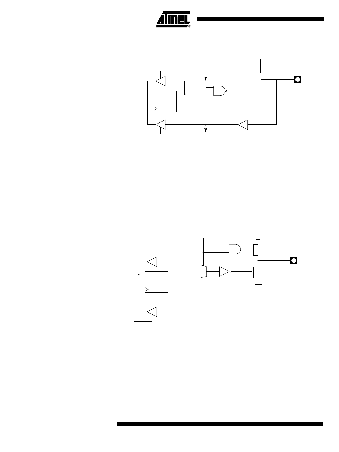
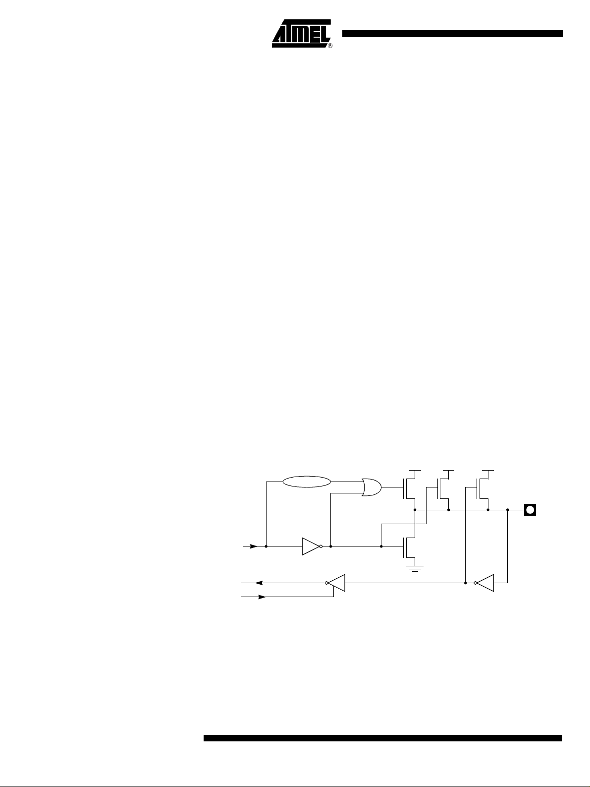
I/O Configurations Each Port SFR operates via type-D latches, as illustrated in Figure 1 for Ports 3 and 4. A
CPU "write to latch" signal initiate s tran sfer of int ernal bus data int o the type -D latch. A
CPU "read latch" signal transfers the latched Q outpu t onto the i nterna l bu s. S im ilar ly, a
"read pin" signal transfers the logical level of the Port pin. Some Port data instructions
activate the "read la tch " signal while others ac tiva te the "r ead pi n" signa l. L atch in structions are referred to as Read-Modify-Write instructions. Each I/O line may be
independently programmed as input or output.
Port 1, Port 3 and Port 4 Figure 1 shows the structur e of Ports 1 and 3, whic h have inter nal pul l-ups. A n externa l
source can pull the pin l ow. Ea ch P ort pi n can be c onfigu red e ither for gene ral-pu rpose
I/O or for its alternate input output function.
To use a pin for general-purpose output, set or clear the corresponding bit in the Px register (x = 1,3 or 4). To use a pi n for gener al-pur pose input, s et the bi t in the Px r egister .
This turns off the output FET drive.
To configure a pin for its al ter nat e fun ction, set the bit in the Px register . W hen the l atch
is set, the "alternate out put functi on" si gnal co ntrols the output lev el (see Fi gure 1) . The
operation of Ports 1, 3 an d 4 is discussed fur the r in the "quasi-Bidirectional Port Operation" section.
4129L–CAN–08/05
7
Page 8
A/T89C51CC01
Figure 1. Port 1, Port 3 and Port 4 Structure
x
x
x
)
VCC
READ
LATCH
ALTERNATE
OUTPUT
FUNCTION
INTERNAL
PULL-UP (1)
P1.
P3.
INTERNAL
BUS
WRITE
TO
LATCH
READ
PIN
D
CL
P3.X
P4.X
LATCH
QP1.X
ALTERNATE
INPUT
FUNCTION
P4.
Note: The internal pull-up can be disabled on P1 when analog function is selected.
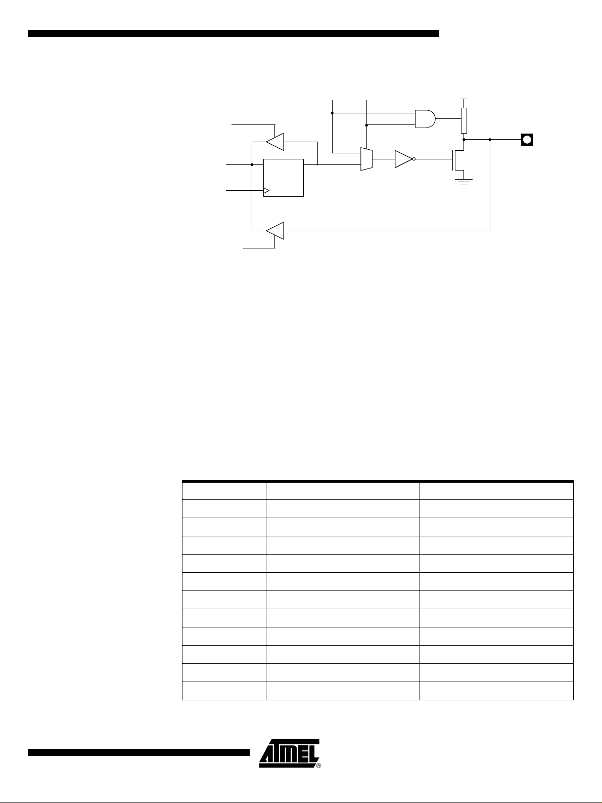
Port 0 and Port 2 Ports 0 and 2 are used for general-purpose I/O or as the external address/data bus. Port
0, shown in Figure 3, differs from the other Ports in not having internal pull-ups. Figure 3
shows the structure of Port 2. An external source can pull a Port 2 pin low.
To use a pin for general-purpose output, set or clear the corresponding bit in the Px register (x = 0 or 2). To use a pin for gen eral -purpos e input , set the bit in the Px r egister to
turn off the output driver FET.
Figure 2. Port 0 Structure
ADDRESS LOW/
DATA
READ
LATCH
INTERNAL
BUS
WRITE
TO
LATCH
READ
PIN
D
P0.X
LATCH
Q
Notes: 1. Port 0 is precluded from use as general-purpose I/O Ports when used as
address/data bus drivers.
2. Port 0 internal strong pull-up s as si st th e log ic -one outp ut for m em ory bus cyc les onl y.
Except for these bus cycles, the pull-up FET is off, Port 0 outputs are open-drain.
CONTROL
1
0
VDD
(2)
P0.x (1
8
4129L–CAN–08/05
Page 9
A/T89C51CC01
Figure 3. Port 2 Structure
READ
LATCH
INTERNAL
BUS
WRITE
TO
LATCH
READ
PIN
D
P2.X
LATCH
ADDRESS HIGH/
Q
CONTROL
1
0
Notes: 1. Port 2 is precluded from use as gen era l-pu r po se I/O Ports when as address /data bus
drivers.
2. Port 2 internal strong pull-ups FET (P1 in FiGURE) assist the logic-one output for
memory bus cycle.
VDD
INTERNAL
PULL-UP (2)
P2.x (1)
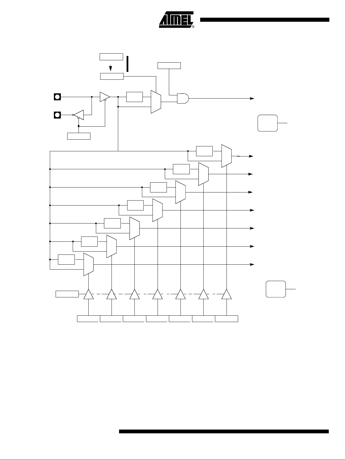
Read-Modify-Write Instructions
When Port 0 and Port 2 are used for an external memory cycle, an internal control signal
switches the output-driver input from the latch output to the internal address/data line.
Some instructions rea d the l atch data rath er th an the pin da ta. T he latch based inst ructions read the data , m odi fy th e d ata and th en r ewrite th e l atc h. Thes e ar e ca ll ed "Re adModify-Write" instructions. Below is a complete list of these special instructions (see
Table ). When the destination operand is a Port or a Port bit, these instructions read the
latch rather than the pin:
Table 2. Re ad-Modify-Write Instruction s
Instruction Description Example
ANL logical AND ANL P1, A
ORL logical OR ORL P2, A
XRL logical EX-OR XRL P3, A
JBC jump if bit = 1 and clear bit J BC P1. 1, LABEL
CPL complement bit CPL P3.0
INC increment INC P2
DEC decrement DEC P2
4129L–CAN–08/05
DJNZ decrement and jump if not zero DJNZ P3, LABEL
MOV Px.y, C move carry bit to bit y of Port x MOV P1.5, C
CLR Px.y clear bit y of Port x CLR P2.4
SET Px.y set bit y of Port x SET P3.3
9
Page 10
A/T89C51CC01
It is not obvious the last three instructions in this list are Read-Modify-Write instructions.
x
x
x
x
These instructions read the port (all 8 bits), modify the specifically addressed bit and
write the new byte back t o the lat ch. Thes e Read- Modif y-Write i nstruc tions a re dire cted
to the latch rather than the pin in order to avoid possible misinterpretation of voltage
(and therefore, logi c) leve ls at th e pin. Fo r exam ple, a P ort bit us ed to dr ive the ba se of
an external bipolar t ransis tor can not rise abov e the tra nsistor’s b ase-emi tter junctio n
voltage (a value lower than VIL). With a logic one written to the bit, attempts by the CPU
to read the Port at the pi n are misinte rpreted as lo gic zero. A rea d of the latch rath er
than the pins returns the correct logic-one value.
Quasi-Bidirectional Port Operation
Port 1, Port 2, Port 3 an d Port 4 have fix ed internal pul l-ups and are ref erred to as
"quasi-bidirection al " Por ts . Wh en c onf igu re d as an inp u t, th e pin impedance appears as
logic one and sources current in response to an external logic zero condition. Port 0 is a
"true bidirectional" pin. The pins float when configured as input. Resets write logic one to
all Port latches. If logi cal zero i s subseque ntly writte n to a Port latch , it can be retur ned
to input conditions by a logical one written to the latch.
Note: Port latch values change near the end of Read-Modify-Write instruction cycles. Output
buffers (and therefore the pin state) update early in the instruction after Read-ModifyWrite instruction cycle.
Logical zero-to-one transitions in Port 1, Port 2, Port 3 and Port 4 use an additional pullup (p1) to aid this logic transition (see Figure 4.). This increases switch speed. This
extra pull-up sources 100 times normal internal circuit current during 2 oscillator clock
periods. The internal pull-ups are field-effect transistors rather than linear resistors. Pullups consist of three p-channel FET (pFET) devices. A pFET is on when the gate senses
logical zero and off when the gate senses logical one. pFET #1 is turned on for two
oscillator periods immediately after a zero-to-one tr ansition in the Port latch. A logical
one at the Port pin turns on pFE T #3 (a we ak pul l-up ) th rough the i nv ert er. T his i nver ter
and pFET pair form a latch to drive logical one. pFET #2 is a very weak pull-up switched
on whenever the associated nF ET is switched off. This is tradi tional CMOS switch convention. Current strengths are 1/10 that of pFET #3.
Figure 4. Internal Pull-Up Configurations
2 Osc. PERIODS
VCCVCCVCC
10
p1(1)
OUTPUT DATA
INPUT DATA
READ PIN
Note: Port 2 p1 assists the logic-one output for memory bus cycles.
p2
n
p3
P1.
P2.
P3.
P4.
4129L–CAN–08/05
Page 11

A/T89C51CC01
SFR Mapping The Special Function Registers (SFRs) of the T89C51CC01 fall into the following
categories:
Table 3. C51 Core SFRs
MnemonicAddName 76543210
ACCE0hAccumulator ––––––––
B F0hB Register ––––––––
PSW D0h Program Status Word CY AC F0 RS1 RS0 OV F1 P
SP81hStack Pointer ––––––––
Data Pointer Low
DPL 82h
DPH 83h
byte
LSB of DPTR
Data Pointer High
byte
MSB of DPTR
––––––––
––––––––
Table 4. I/O Port SFRs
MnemonicAddName 76543210
P080hPort 0 ––––––––
P190hPort 1 ––––––––
P2A0hPort 2 ––––––––
P3B0hPort 3 ––––––––
P4C0hPort 4 (x2) ––––––––
Table 5. Timers SFRs
MnemonicAddName 76543210
TH0 8Ch
TL0 8Ah
TH1 8Dh
TL1 8Bh
TH2 CDh
Timer/Counter 0 High
byte
Timer/Counter 0 Low
byte
Timer/Counter 1 High
byte
Timer/Counter 1 Low
byte
Timer/Counter 2 High
byte
––––––––
––––––––
––––––––
––––––––
––––––––
TL2 CCh
TCON 88h
TMOD 89h
4129L–CAN–08/05
Timer/Counter 2 Low
byte
Timer/Counter 0 and
1 control
Timer/Counter 0 and
1 Modes
––––––––
TF1 TR1 TF0 TR0 IE1 IT1 IE0 IT0
GATE1 C/T1# M11 M01 GATE0 C/T0# M10 M00
11
Page 12

A/T89C51CC01
Table 5. Timers SFRs (Continued)
MnemonicAddName 76543210
T2CON C8h
T2MOD C9h
RCAP2H CBh
RCAP2L CAh
WDTRST A6h
WDTPRG A7h
Timer/Counter 2
control
Timer/Counter 2
Mode
Timer/Counter 2
Reload/Capture High
byte
Timer/Counter 2
Reload/Capture Low
byte
Watchdog Timer
Reset
Watchdog Timer
Program
TF2 EXF2 RCLK TCLK EXEN2 TR2 C/T2# CP/RL2#
––––––T2OEDCEN
––––––––
––––––––
––––––––
–––––S2S1S0
Table 6. Serial I/O Port SFRs
MnemonicAddName 76543210
SCON 98h Serial Control FE/SM0 SM1 SM2 REN TB8 RB8 TI RI
SBUF99hSerial Data Buffer––––––––
SADEN B9h Slave Addres s Mask – – – – – – – –
SADDRA9hSlave Address ––––––––
Table 7. P CA SF Rs
Mnemonic
CCON D8h PCA Timer/Counter Control CF CR – CCF4 CCF3 CCF2 CCF1 CCF0
CMOD D9h PCA Timer/Counter Mode CIDL WDTE – – – CPS1 CPS0 ECF
CL E9h PCA Timer/Counter Low byte ––––––––
CH F9h PCA Timer/Counter High byte ––––––––
CCAPM0
CCAPM1
CCAPM2
CCAPM3
CCAPM4
CCAP0H
CCAP1H
CCAP2H
CCAP3H
CCAP4H
AddName 76543210
DAh
PCA Timer/Counter Mode 0
DBh
PCA Timer/Counter Mode 1
DCh
PCA Timer/Counter Mode 2
DDh
PCA Timer/Counter Mode 3
DEh
PCA Timer/Counter Mode 4
FAh
PCA Compare Capture Module 0 H
FBh
PCA Compare Capture Module 1 H
FCh
PCA Compare Capture Module 2 H
FDh
PCA Compare Capture Module 3 H
FEh
PCA Compare Capture Module 4 H
CCAP0H7
CCAP1H7
CCAP2H7
CCAP3H7
CCAP4H7
–
ECOM0
ECOM1
ECOM2
ECOM3
ECOM4
CCAP0H6
CCAP1H6
CCAP2H6
CCAP3H6
CCAP4H6
CAPP0
CAPP1
CAPP2
CAPP3
CAPP4
CCAP0H5
CCAP1H5
CCAP2H5
CCAP3H5
CCAP4H5
CAPN0
CAPN1
CAPN2
CAPN3
CAPN4
CCAP0H4
CCAP1H4
CCAP2H4
CCAP3H4
CCAP4H4
MAT0
MAT1
MAT2
MAT3
MAT4
CCAP0H3
CCAP1H3
CCAP2H3
CCAP3H3
CCAP4H3
TOG0
TOG1
TOG2
TOG3
TOG4
CCAP0H2
CCAP1H2
CCAP2H2
CCAP3H2
CCAP4H2
PWM0
PWM1
PWM2
PWM3
PWM4
CCAP0H1
CCAP1H1
CCAP2H1
CCAP3H1
CCAP4H1
ECCF0
ECCF1
ECCF2
ECCF3
ECCF4
CCAP0H0
CCAP1H0
CCAP2H0
CCAP3H0
CCAP4H0
12
4129L–CAN–08/05
Page 13

Table 7. P CA SFRs (Cont inu ed)
Mnemonic
AddName 76543210
A/T89C51CC01
CCAP0L
CCAP1L
CCAP2L
CCAP3L
CCAP4L
EAh
PCA Compare Capture Module 0 L
EBh
PCA Compare Capture Module 1 L
ECh
PCA Compare Capture Module 2 L
EDh
PCA Compare Capture Module 3 L
EEh
PCA Compare Capture Module 4 L
CCAP0L7
CCAP1L7
CCAP2L7
CCAP3L7
CCAP4L7
CCAP0L6
CCAP1L6
CCAP2L6
CCAP3L6
CCAP4L6
CCAP0L5
CCAP1L5
CCAP2L5
CCAP3L5
CCAP4L5
CCAP0L4
CCAP1L4
CCAP2L4
CCAP3L4
CCAP4L4
CCAP0L3
CCAP1L3
CCAP2L3
CCAP3L3
CCAP4L3
CCAP0L2
CCAP1L2
CCAP2L2
CCAP3L2
CCAP4L2
CCAP0L1
CCAP1L1
CCAP2L1
CCAP3L1
CCAP4L1
CCAP0L0
CCAP1L0
CCAP2L0
CCAP3L0
CCAP4L0
Table 8. Interrupt SFRs
MnemonicAddName 76543210
IEN0 A8h
IEN1 E8h
IPL0 B8h
IPH0 B7h
IPL1 F8h
IPH1 F7h
Interrupt Enable
Control 0
Interrupt Enable
Control 1
Interrupt Priorit y
Control Low 0
Interrupt Priorit y
Control High 0
Interrupt Priorit y
Control Low 1
Interrupt Priorit y
Control High1
EA EC ET2 ES ET1 EX1 ET0 EX0
– – – – – ETIM EADC ECAN
– PPC PT2 PS PT1 PX1 PT0 PX0
– PPCH PT2H PSH PT1H PX1H PT0H PX0H
– – – – – POVRL PADCL PCANL
–––––POVRHPADCHPCANH
Table 9. ADC SFRs
MnemonicAddName 76543210
ADCON F3h ADC Control – PSIDLE ADEN ADEOC ADSST SCH2 SCH1 SCH0
ADCF F6h ADC Configuration CH7 CH6 CH5 CH4 CH3 CH2 CH1 CH0
ADCLK F2h ADC Clock – – – PRS4 PRS3 PRS 2 PRS1 PRS0
ADDH F5h ADC Data High byte ADAT9 ADAT8 ADAT7 A DAT6 ADAT5 ADAT4 A DAT3 ADAT2
ADDL F4h ADC Data Low byte – – – – – – ADAT1 ADAT0
Table 10. CAN SFRs
MnemonicAddName 76543210
CANGCON ABh
CANGSTA AAh
CANGIT 9Bh
CANBT1 B4h CAN Bit Timing 1 – BRP5 BRP4 BRP3 BRP2 BRP1 BRP0 –
CANBT2 B5h CAN Bit Timing 2 – SJW1 SJW0 – PRS2 PRS1 PRS0 –
CAN General
Control
CAN General
Status
CAN General
Interrupt
ABRQ OVRQ TTC SYNCTTC
– OVFG – TBSY RBSY ENFG BOFF ERRP
CANIT – OVRTIM OVRBUF SERG CERG FERG AERG
AUT–
BAUD
TEST ENA GRES
CANBT3 B6h CAN Bit Timing 3 – PHS22 PHS21 PHS20 PHS12 PHS11 PHS10 SMP
4129L–CAN–08/05
13
Page 14

A/T89C51CC01
Table 10. CAN SFRs (Continued)
MnemonicAddName 76543210
CANEN1 CEh
CANEN2 CFh
CANGIE C1h
CANIE1 C2h
CANIE2 C3h
CANSIT1 BA h
CANSIT2 BB h
CANTCON A1h
CANTIMH ADh CAN Timer high
CAN Enable
Channel byte 1
CAN Enable
Channel byte 2
CAN General
Interrupt Enable
CAN Interrupt
Enable Channel
byte 1
CAN Interrupt
Enable Channel
byte 2
CAN Status
Interrupt Channel
byte1
CAN Status
Interrupt Channel
byte2
CAN Timer
Control
– ENCH14 ENCH13 ENCH12 ENCH11 ENCH10 ENCH9 ENCH8
ENCH7 ENCH6 ENCH5 ENCH4 ENCH3 ENCH2 ENCH1 ENCH0
– – ENRX ENTX ENERCH ENBUF ENERG –
– IECH14 IECH13 IECH12 IECH11 IECH10 IECH9 IECH8
IECH7 IECH6 IECH5 IECH4 IECH3 IECH2 IECH1 IECH0
– SIT14 SIT13 SIT12 SIT11 SIT10 S IT 9 SIT8
SIT7 SIT6 SIT5 SIT4 SIT3 SIT2 SIT1 SIT0
TPRESC 7 TPRESC 6 TPRESC 5 TPRESC 4 TPRESC 3 TPRESC 2 TPRESC 1 TPRESC 0
CANTIM 15CANTIM 14CANTIM 13CANTIM 12CANTIM 11CANTIM 10CANTIM 9CANTIM
8
CANTIML ACh CAN Timer low CANTIM 7 CANTIM 6 CANTIM 5 CANTIM 4 CANTIM 3 CANTIM 2 CANTIM 1 CANTIM 0
CANSTMH AFh
CANSTML AEh
CANTTCH A5h
CANTTCL A4h
CANTEC 9Ch
CANREC 9Dh
CANPAGE B1h CAN Page CHNB3 CHNB2 CHNB1 CHNB0 AINC INDX2 INDX1 INDX0
CANSTCH B2h
CANCONH B3h
CANMSG A3h
CAN Timer Stamp
high
CAN Timer Stamp
low
CAN Timer TTC
high
CAN Timer TTC
low
CAN Transmit
Error Counter
CAN Receive
Error Counter
CAN Status
Channel
CAN Control
Channel
CAN Message
Data
TIMSTMP 15TIMSTMP 14TIMSTMP 13TIMSTMP 12TIMSTMP 11TIMSTMP 10TIMSTMP 9TIMSTMP
TIMSTMP7TIMSTMP 6TIMSTMP 5TIMSTMP 4TIMSTMP 3TIMSTMP 2TIMSTMP 1TIMSTMP
TIMTTC 15 TIMTTC 14 TIMTTC 13 TIMTTC 12 TIMTTC 11 TIMTTC 1 0 TIM TTC 9 TIMTTC 8
TIMTTC
7
TEC7 TEC6 TEC5 TEC4 TEC3 TEC2 TEC1 TEC0
REC7 REC6 REC5 REC4 REC3 REC2 REC1 REC0
DLCW TXOK RXOK BERR SERR CERR FERR AERR
CONCH1 CONCH0 RPLV IDE DLC3 DLC2 DLC1 DLC0
MSG7 MSG6 MSG5 MSG4 MSG3 MSG2 MSG1 MSG0
TIMTTC
6
TIMTTC5TIMTTC
4
TIMTTC
3
TIMTTC
2
TIMTTC1TIMTTC
8
0
0
14
4129L–CAN–08/05
Page 15

A/T89C51CC01
Table 10. CAN SFRs (Continued)
MnemonicAddName 76543210
CANIDT1 BCh
CANIDT2 BDh
CANIDT3 BEh
CANIDT4 BFh
CANIDM1 C4h
CANIDM2 C5h
CAN Identifier T ag
byte 1(Part A)
CAN Identifier T ag
byte 1(PartB)
CAN Identifier T ag
byte 2 (PartA)
CAN Identifier T ag
byte 2 (PartB)
CAN Identifier T ag
byte 3(PartA)
CAN Identifier T ag
byte 3(PartB)
CAN Identifier T ag
byte 4(PartA)
CAN Identifier T ag
byte 4(PartB)
CAN Identifier
Mask byte
1(PartA)
CAN Identifier
Mask byte
1(PartB)
CAN Identifier
Mask byte
2(PartA)
CAN Identifier
Mask byte
2(PartB)
IDT10 IDT9 IDT8 IDT7 IDT6 IDT5 IDT4 IDT3
IDT28 IDT27 IDT26 IDT25 IDT24 IDT23 IDT22 IDT21
IDT2
IDT20
–
IDT12
–
IDT4
IDMSK10
IDMSK28
IDMSK2
IDMSK20
IDT1
IDT19
–
IDT11
–
IDT3
IDMSK9
IDMSK27
IDMSK1
IDMSK19
IDT0
IDT18
–
IDT10
–
IDT2
IDMSK8
IDMSK26
IDMSK0
IDMSK18–IDMSK17–IDMSK16–IDMSK15–IDMSK14–IDMSK13
–
IDT17
–
IDT9
–
IDT1
IDMSK7
IDMSK25
–
IDT16
–
IDT8
–
IDT0
IDMSK6
IDMSK24
–
IDT15
–
IDT7
RTRTAG
–
IDMSK5
IDMSK23
–
IDT14
–
IDT6
–
RB1TAG
IDMSK4
IDMSK22
IDT13
RB0TAG
IDMSK3
IDMSK21
–
–
IDT5
–
CAN Identifier
CANIDM3 C6h
CANIDM4 C7h
Mask byte
3(PartA)
CAN Identifier
Mask byte
3(PartB)
CAN Identifier
Mask byte
4(PartA)
CAN Identifier
Mask byte
4(PartB)
–
IDMSK12–IDMSK11–IDMSK10–IDMSK9–IDMSK8–IDMSK7
–
IDMSK4
–
IDMSK3–IDMSK2
–
IDMSK1–IDMSK0
RTRMSK
–
–
IDMSK6–IDMSK5
–IDEMSK
–
Table 11. Other SFRs
MnemonicAddName 76543210
PCON 87h Power Control SMOD1 SMOD0 – POF GF1 GF0 PD IDL
AUXR 8Eh Auxiliary Register 0 – – M0 – XRS1 XRS2 EXTRAM A0
AUXR1 A2h Auxiliary Register 1 – – ENBOOT – GF3 0 – DPS
CKCON 8Fh Clock Control CANX2 W DX 2 P C AX 2 SIX2 T2X2 T1X2 T0X2 X2
4129L–CAN–08/05
15
Page 16

A/T89C51CC01
Table 11. Other SFRs
MnemonicAddName 76543210
FCON D1h Flash Control FPL3 FPL2 FPL1 FPL0 FPS FMOD1 FMOD0 FBUSY
EECON D2h EEPROM Contol EEPL3 EEPL2 EEPL1 EEPL0 – – EEE EEBUSY
Table 12. SFR Mapping
(1)
0/8
1/9 2/A 3/B 4/C 5/D 6/E 7/F
F8h
F0h
E8h
E0h
D8h
D0h
C8h
C0h
B8h
B0h
A8h
IPL1
xxxx x000
B
0000 0000
IEN1
xxxx x000
ACC
0000 0000
CCON
00x0 0000
PSW
0000 0000
T2CON
0000 0000
P4
xxxx xx11
IPL0
x000 0000
P3
1111 1111
IEN0
0000 0000
CH
0000 0000
CL
0000 0000
CMOD
00xx x000
FCON
0000 0000
T2MOD
xxxx xx00
CANGIE
11000000
SADEN
0000 0000
CANPAGE
0000 0000
SADDR
0000 0000
CCAP0H
0000 0000
ADCLK
xxx0 0000
CCAP0L
0000 0000
CCAPM0
x000 0000
EECON
xxxx xx00
RCAP2L
0000 0000
CANIE1
x000 0000
CANSIT1
x000 0000
CANSTCH
xxxx xxxx
CANGSTA
1010 0000
CCAP1H
0000 0000
ADCON
x000 0000
CCAP1L
0000 0000
CCAPM1
x000 0000
RCAP2H
0000 0000
CANIE2
0000 0000
CANSIT2
0000 0000
CANCONCH
xxxx xxxx
CANGCON
0000 0000
CCAP2H
0000 0000
ADDL
0000 0000
CCAP2L
0000 0000
CCAPM2
x000 0000
TL2
0000 0000
CANIDM1
xxxx xxxx
CANIDT1
xxxx xxxx
CANBT1
xxxx xxxx
CANTIML
0000 0000
CCAP3H
0000 0000
ADDH
0000 0000
CCAP3L
0000 0000
CCAPM3
x000 0000
TH2
0000 0000
CANIDM2
xxxx xxxx
CANIDT2
xxxx xxxx
CANBT2
xxxx xxxx
CANTIMH
0000 0000
CCAP4H
0000 0000
ADCF
0000 0000
CCAP4L
0000 0000
CCAPM4
x000 0000
CANEN1
x000 0000
CANIDM3
xxxx xxxx
CANIDT3
xxxx xxxx
CANBT3
xxxx xxxx
CANSTMPL
xxxx xxxx
IPH1
xxxx x000
CANEN2
0000 0000
CANIDM4
xxxx xxxx
CANIDT4
xxxx xxxx
IPH0
x000 0000
CANSTMPH
xxxx xxxx
FFh
F7h
EFh
E7h
DFh
D7h
CFh
C7h
BFh
B7h
AFh
A0h
98h
90h
88h
80h
P2
1111 1111
SCON
0000 0000
P1
1111 1111
TCON
0000 0000
P0
1111 1111
(1)
0/8
CANTCON
0000 0000
SBUF
0000 0000
TMOD
0000 0000
SP
0000 0111
1/9 2/A 3/B 4/C 5/D 6/E 7/F
Reserved
Note: 1. These registers are bit–addressable.
Sixteen addresses in the SFR space are both byte
whose address ends in 0 and 8. The bit addresses, in this area, are 0x80 through to 0xFF.
16
AUXR1
xxxx 00x0
TL0
0000 0000
DPL
0000 0000
CANMSG
xxxx xxxx
CANGIT
0x00 0000
TL1
0000 0000
DPH
0000 0000
CANTTCL
0000 0000
CANTEC
0000 0000
TH0
0000 0000
–addressable and bit–addressable. The bit–addressable SFR’s are those
CANTTCH
0000 0000
CANREC
0000 0000
TH1
0000 0000
WDTRST
1111 1111
AUXR
x00x 1100
WDTPRG
xxxx x000
CKCON
0000 0000
PCON
00x1 0000
4129L–CAN–08/05
A7h
9Fh
97h
8Fh
87h
Page 17

A/T89C51CC01
Clock The T89C51CC01 core needs only 6 clock periods per machine cycl e. This feature,
called ”X2”, provides the following advantages:
• Divides frequency crystals by 2 (cheaper crystals) while keeping the same CPU
power.
• Saves power consumption while keeping the same CPU power (oscillator power
saving).
• Saves power consumption by dividing dynamic operating frequency by 2 in
operating and idle modes.
• Increases CPU power by 2 while keeping the same crystal frequency.
In order to keep the ori ginal C51 com patibil ity, a divider -by-2 is in serted betwe en the
XTAL1 signal and the main clock input of the core (phase generator). This divider may
be disabled by the software.
An extra feature is available to start after Reset in the X2 mode. This feature can be
enabled by a bit X2B in the Hardware Sec urity Byte. Thi s bit is described in the section
"In-System-Programming".
Description T he X2 bit in the CK CON regis ter (see Tabl e 13) allo ws switching from 12 cloc k cycles
per instruction to 6 clock cycles and vice versa. At reset, the standard speed is activated
(STD mode).
Setting this bit activates the X2 feature (X2 mode) for the CPU Clock only (see Figure
5.).
The Timers 0, 1 and 2, Uart, PCA, W atchdog or CAN switch in X 2 mode onl y if the co rresponding bit is cleared in the CKCON register.
The clock for the whole circuit and peripheral is first divided by two before being used by
the CPU core and peripherals. This allows any cyclic ratio to be accepted on the XTAL1
input. In X2 mode, as thi s divid er is bypas s ed, t he s ig nal s o n XTA L1 m us t hav e a cy clic
ratio between 40 to 60%. Figure 5. shows the clock generation block diagram. The X2
bit is validated on the XTAL1÷2 rising edge to avoid glitches when switching from the X2
to the STD mode. Figure 6 shows the mode switching waveforms.
4129L–CAN–08/05
17
Page 18
A/T89C51CC01
Figure 5. Clock CPU Generation Diagram
X
X
X2B
Hardware byte
On RESET
PCON.0
IDL
X2
CKCON.0
TAL1
÷ 2
0
1
CPU Core
Clock
TAL2
CPU
CLOCK
PD
PCON.1
÷ 2
÷ 2
÷ 2
÷ 2
÷ 2
÷ 2
1
0
÷ 2
1
0
1
0
1
0
1
0
1
0
CPU Core Clock Symbol
1
0
FT0 Clock
FT1 Clock
FT2 Clock
FUart Clock
FPca Cloc k
FWd Clock
FCan Clock
and ADC
18
X2
CKCON.0
CANX2
CKCON.7
WDX2
CKCON.6
PCAX2
CKCON.5
SIX2
CKCON.4
T2X2
CKCON.3
T1X2
CKCON.2
PERIPH
CLOCK
Peripheral Clock Symbol
T0X2
CKCON.1
4129L–CAN–08/05
Page 19
A/T89C51CC01
Figure 6. Mode Switching Waveforms
XTAL1
XTAL1/2
X2 bit
CPU clock
X2 ModeSTD Mode STD Mode
Note: In order to prevent any incorrect operation while operating in the X2 mode, users must be aware that all peripherals using the
clock frequency as a time reference (UART, timers...) will have their time reference divided by two. For example a free running
timer generating an interrupt every 20 ms will then generate an interrupt every 10 ms. A UART with a 4800 baud rate will have
a 9600 baud rate.
4129L–CAN–08/05
19
Page 20

A/T89C51CC01
Register Table 13. CKCON Register
CKCON (S:8Fh)
Clock Control Register
76543210
CANX2 WDX2 PCAX2 SIX2 T2X2 T1X2 T0X2 X2
Bit
Number
7CANX2
6WDX2
5PCAX2
4SIX2
3T2X2
2T1X2
1T0X2
Bit
Mnemonic Description
CAN clock
Clear to select 6 clock periods per peripheral clock cycle.
Set to select 12 clock periods per peripheral clock cycle.
Watchdog clock
Clear to select 6 clock periods per peripheral clock cycle.
Set to select 12 clock periods per peripheral clock cycle.
Programmable Counter Arra y cl oc k
Clear to select 6 clock periods per peripheral clock cycle.
Set to select 12 clock periods per peripheral clock cycle.
Enhanced UART clock (MODE 0 and 2)
Clear to select 6 clock periods per peripheral clock cycle.
Set to select 12 clock periods per peripheral clock cycle.
Timer 2 clock
Clear to select 6 clock periods per peripheral clock cycle.
Set to select 12 clock periods per peripheral clock cycle.
Timer 1 clock
Clear to select 6 clock periods per peripheral clock cycle.
Set to select 12 clock periods per peripheral clock cycle.
Timer 0 clock
Clear to select 6 clock periods per peripheral clock cycle.
Set to select 12 clock periods per peripheral clock cycle.
(1)
(1)
(1)
(1)
(1)
(1)
(1)
20
CPU clock
0X2
Clear to select 12 clock periods per machine cycle (STD mode) for CPU and all
the peripherals.
Set to select 6 clock periods per machine cycle (X2 mode) and to enable the
individual peripherals "X2"bits.
Note: 1. This control bit is vali dated when the CPU clock bit X2 is set; when X2 is low, this bit
has no effect.
Reset Value = 0000 0000b
4129L–CAN–08/05
Page 21
A/T89C51CC01
0
Power Management Two power reduction modes are implemented in the T89C51CC01: the Idle mode and
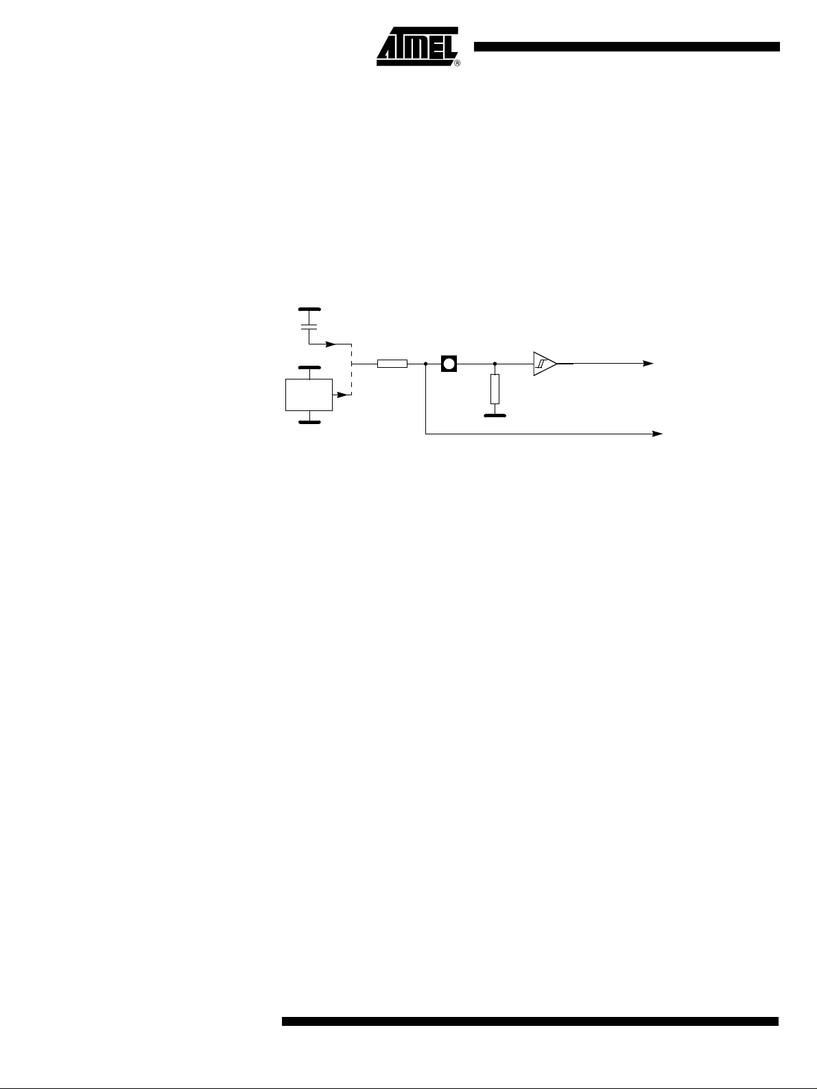
the Power-do wn mode . These modes ar e detai led in th e follo wing se ction s. In ad dition
to these power redu cti on mo des , t he cl oc ks o f th e c ore and peripherals can be dy nam ically divided by 2 using the X2 Mode detailed in Section “Clock”.
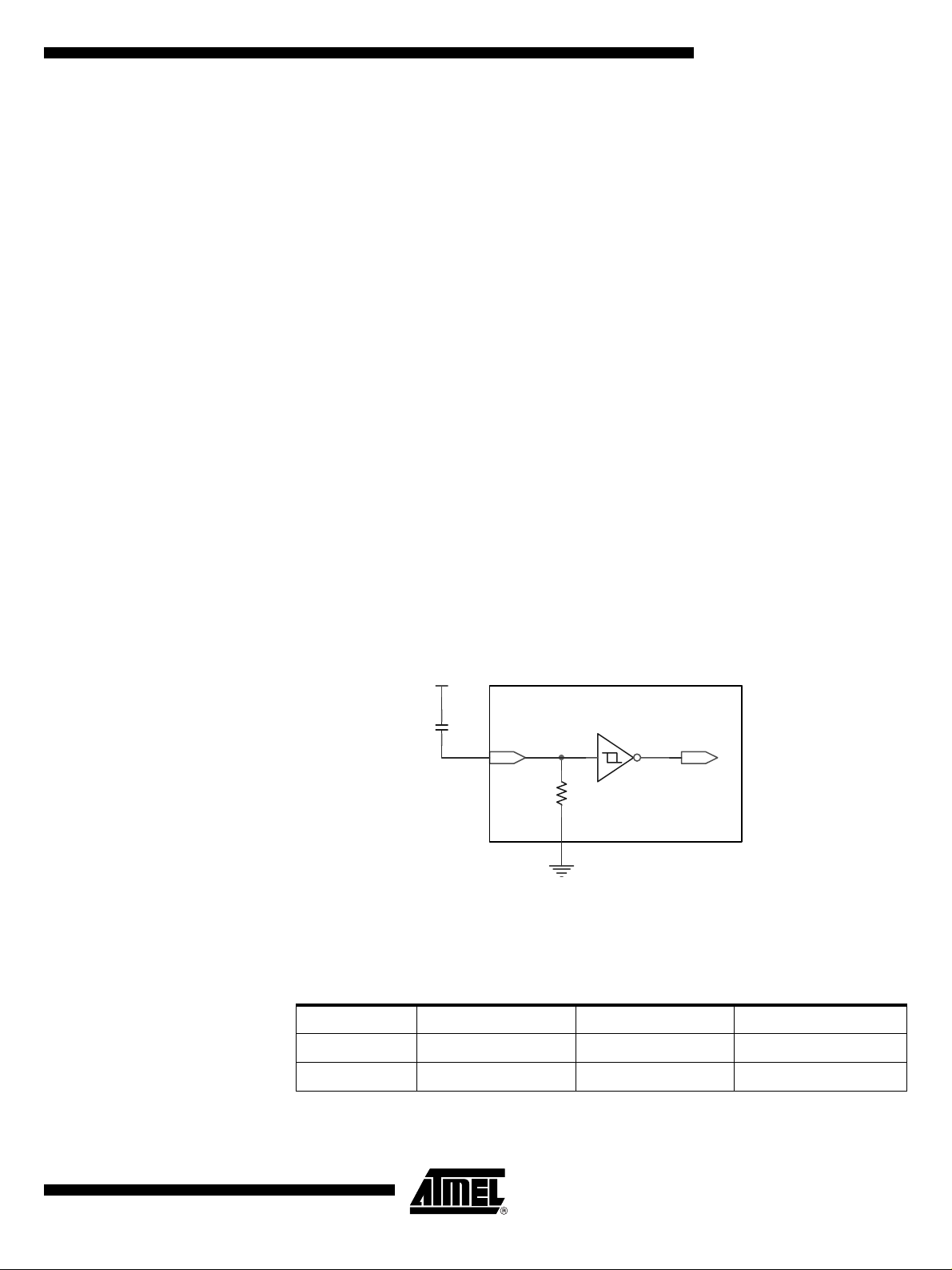
Reset Pin In order to st art-up (col d rese t) or to restart (war m rese t) p roperl y the micr ocont roller , a
high level has to be applied on the RST pin. A bad level leads to a wrong initialisation of
the internal registers like S F Rs, P C, etc . and to unp re dicta ble behavior of the microcontroller. A warm reset ca n be applied either dir ectly o n the RST pin or indire ctly by an
internal reset source such as a watchdog, PCA, timer, etc.
At Power-up (Cold Reset) Two conditions are required before enabling a CPU start-up:
• VDD must reach the specified VDD range,
• The level on xtal1 input must be outside the specification (VIH, VIL).
If one of these two conditions are not met, the microcontroller d oes not start cor rectly
and can execute an instruct ion fetch fro m anywhe re in the progr am spac e. An active
level applied on the RST pin must be mainta ined unti l both of th e above c onditi ons are
met. A reset is active wh en the lev el VIH1 is reached an d when the pu lse width c overs
the period of time where VDD and the oscillator are not stabilized. Two parameters have
to be taken into account to determine the reset pulse width:
• VDD rise time (vddrst),
• Oscillator startup time (oscrst).
To determine the capacitor the highest value of these two parameters has to be chosen.
The reset circuitry is shown in Figure 7.
Figure 7. Reset Circuitry
VDD
Crst
RST pin
Rrst
Reset input circuitry
Internal reset
Table 14 and Table 15 give some typical examples for three values of VDD rise times,
two values of oscillator start-up time and two pull-down resistor values.
Table 14. Minimum Reset Capacitor for a 15k Pull-down Resistor
oscrst/vddrst 1ms 10ms 100ms
5ms 2.7µF 4.7µF 47µF
4129L–CAN–08/05
20ms 10µF 15µF 47µF
Note: These values assume VDD starts from 0v to the nominal value. If the time between two
on/off sequences is too fast, the power-supply de coupling capacitors may not be fully
discharged, leading to a bad reset sequence.
21
Page 22
A/T89C51CC01
Warm Reset To achieve a valid reset, the reset signal must be maintained for at least 2 machine
cycles (24 oscillator clock periods) while the oscillator is running. The number of clock
periods is mode independent (X2 or X1).
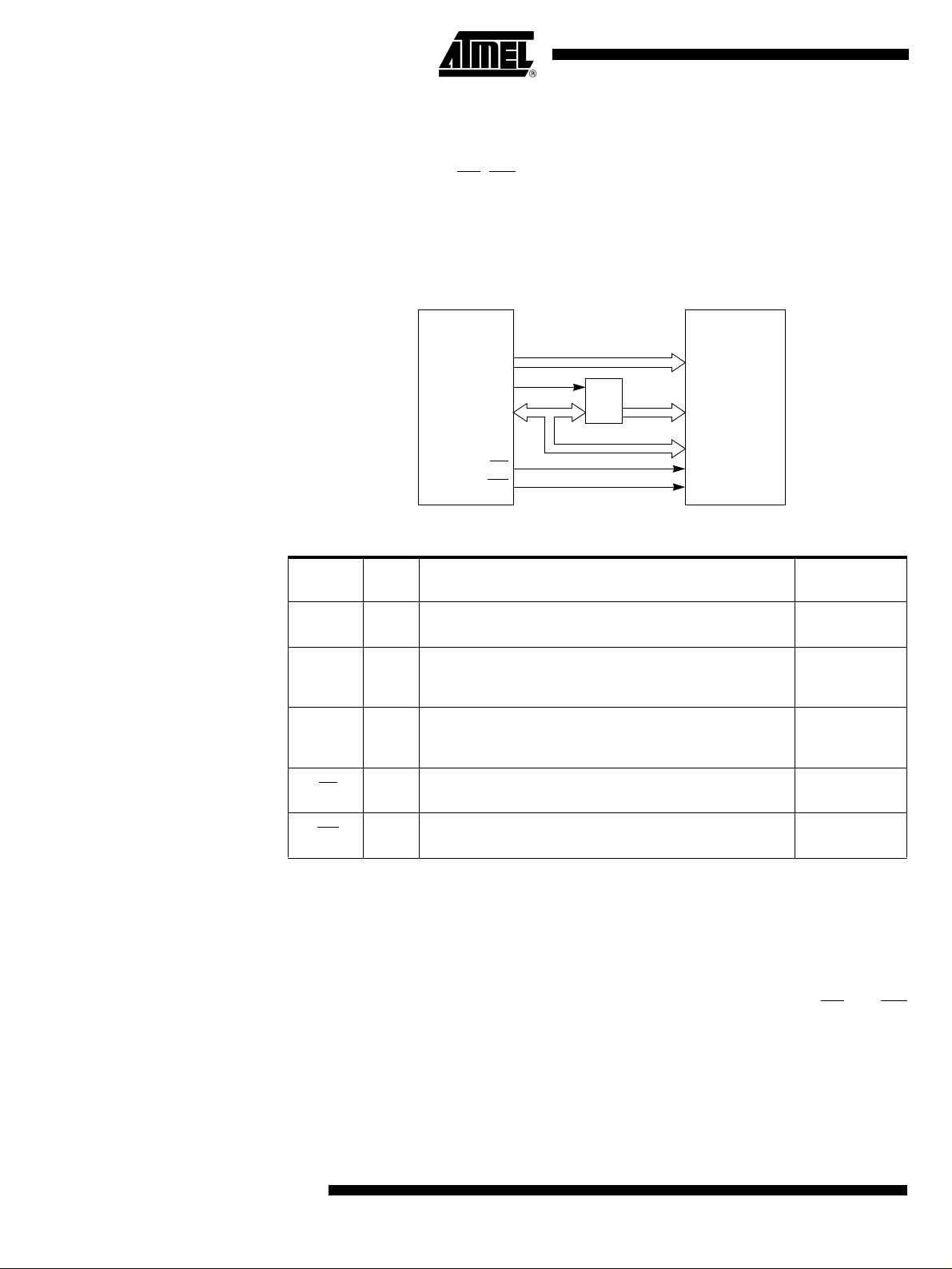
Watchdog Reset As detailed in Section “PCA Watchdog Timer”, page 127, the WDT generates a 96-clock
period pulse on the RST p in. In ord er to prop erly p ropa gate this pu lse to th e re st of the
application in case of external capacitor or power-supply supervisor circuit, a 1KΩ resistor must be added as shown Figure 8.
Figure 8. Reset Circuitry for WDT reset out usage
VDD
+
Reset Recommendation to Prevent Flash Corruption
VDD
VSS
1K
RST
RST
VSS
RST
R
An example of bad initialization situation may occur in an instance where the bit
ENBOOT in AUXR1 registe r is initiali zed from the har dware bit BLJB upon reset. Sinc e
this bit allows mapping of the bootloader in the code area, a reset failure can be critical.
To CPU core
and peripherals
To other
on-board
circuitry
If one wants the ENBOOT cleared in order to unmap the boot from the code area (yet
due to a bad reset) the b it ENBOOT in SFRs may be set. If the value of Progra m
Counter is accidently in th e range of t he boot memory addresses the n a flash a ccess
(write or erase) may corrupt the Flash on-chip memory.
It is recommended to use an external reset circuitry featuring power supply monitoring to
prevent system malfunction during periods of insufficient power supply voltage (power
supply failure, power supply switched off).
Idle Mode Idle mode is a power reduction mode that reduces the power consumption. In this mode,
program execution halts. Idle mode freezes the cl ock to the CPU at known sta tes while
the peripherals continue to be clocked. The CPU status before entering Idle mode is
preserved, i.e., the program counter and program status word register retain their data
for the duration of Idle mode. The contents of the SFRs and RAM are also retained. The
status of the Port pins during Idle mode is detailed in Table 14.
Entering Idle Mode To enter Idle mode, you must set the IDL bit in PCON regi ster (see Table 15 ). The
T89C51CC01 enters Idle mode upon execution of the instruction that sets IDL bit. The
instruction that sets IDL bit is the last instruction executed.
Note: If IDL bit and PD bit are set simultaneously, the T89C51CC01 enters Power-down mode.
Then it does not go in Idle mode when exiting Power-down mode.
Exiting Idle Mode There are two ways to exit Idle mode:
1. Generate an enabled interrupt.
– Hardware clears IDL bit in PCON register which restores the clock to the
CPU. Execution resumes with the interrupt service routine. Upon completion
22
4129L–CAN–08/05
Page 23

A/T89C51CC01
of the interrupt service routine, program execution resumes with the
instruction immediately following the instruction that activated Idle mode.
The general-purpose flags (GF1 and GF0 in PCON register) may be used to
indicate whether an interrupt occurred during normal operation or during Idle
mode. When Idle mode is exited by an interrupt, the interrupt service routine
may examine GF1 and GF0.
2. Generate a reset.
– A logic high on the RST pin clears IDL bit in PCON register directly and
asynchronously. This restores the clock to the CPU. Program execution
momentarily resumes with the instruction immediately following the
instruction that activated the Idle mode and may continue for a number of
clock cycles before the internal reset algorithm takes control. Reset
initializes the T89C51CC01 and vectors the CPU to address C:0000h.
Note: 1. During the time that execution resumes, the internal RAM cannot be accessed; how-
ever, it is possible for the Port pins to be accessed. To avoid unexpected outputs at
the Port pins, the instruction immediately following the instruction that activated Idle
mode should not write to a Port pin or to the external RAM.
2. If Idle mode is invoked by ADC Idle, the ADC conversion completion will exit Idle.
Power-down Mode The Power-down mode places the T89C51CC01 in a very low power state. Power-down
mode stops the oscillator and freezes all clocks at known states. The CPU status prior to
entering Power-down mode is preserved, i.e., the program cou nter, program status
word register retain their data for the duration of Power-down mode. In addition, the
SFRs and RAM content s a re pres erv ed. T h e s tatu s of the Po rt pins dur in g P ower -do w n
mode is detailed in Table 14.
Entering Power-down Mode To enter Power-d own mode , set PD bi t in PCO N regist er. The T 89C51CC0 1 enter s the
Power-down mo de upon ex ecution of t he inst ruction th at sets PD bi t. The inst ruction
that sets PD bit is the last instruction executed.
Exiting Power-down Mode If VDD was reduced during the Power-down mode, do not exit Power-down mode until
VDD is restored to the normal operating level.
There are two ways to exit the Power-down mode:
1. Generate an enabled external interrupt.
– The T89C51CC01 provides capability to exit from Power-down using INT0#,
INT1#.
Hardware clears PD bit in PCON register which starts the oscillator and
restores the clocks to the CPU and peripherals. Using INTx# input,
execution resumes when the input is released (see Figure 9) while using
KINx input, execution resumes after counting 1024 clock ensuring the
oscillator is restarted properly (see Figure 8). Execution resumes with the
interrupt service routine. Upon completion of the interrupt service routine,
program execution resumes with the instruction immediately following the
instruction that activated Power-down mode.
4129L–CAN–08/05
Note: 1. The external interrupt used to exit Power-down mode must be configured as level
sensitive (INT0# and INT1#) and must be assigned the highest priority. In addition,
the duration of the interrupt must be long enough to allow the oscillator to stabilize.
The execution will only resume when the interrupt is deasserted.
2. Exit from power-down by external interrupt does not affect the SFRs nor the internal
RAM content.
23
Page 24

A/T89C51CC01
Figure 9. Power-down Exit Waveform Using INT1:0#
INT1:0#
OSC
Power-down phase Oscillator restart phase Active phaseActive phase
2. Generate a reset.
– A logic high on the RST pin clears PD bit in PCON register directly and
asynchronously. This starts the oscillator and restores the clock to the CPU
and peripherals. Program execution momentarily resumes with the
instruction immediately following the instruction that activated Power-down
mode and may continue for a number of clock cycles before the internal
reset algorithm takes control. Reset initializes the T89C51CC01 and vectors
the CPU to address 0000h.
Notes: 1. D ur i ng the t im e th at ex e cuti o n re su me s, th e i nt er na l R AM ca n no t be ac ce ss ed ; ho w -
ever, it is possible for the Port pins to be accessed. To avoid unexpected outputs at
the Port pins, the instruction immediately following the instruction that activated the
Power-down mode should not write to a Port pin or to the external RAM.
2. Exit from power-down by res et r ede fine s all the SFRs, but does not affect the inte rna l
RAM content.
24
4129L–CAN–08/05
Page 25

Registers Table 15. PCON Register
PCON (S:87h) – Power configuration Register
76543210
SMOD1 SMOD0 - POF GF1 GF0 PD IDL
A/T89C51CC01
Bit
Number
7SMOD1
6SMOD0
5-
4POF
3GF1
2GF0
1PD
Bit
Mnemonic Description
Serial port Mode bit 1
Set to select double baud rate in mode 1, 2 or 3
Serial port Mode bit 0
Clear to select SM0 bit in SCON register.
Set to select FE bit in SCON register.
Reserved
The value read from this bit is indeterminate. Do not set this bit.
Power-Off Flag
Clear to recognize next reset type.
Set by hardware when V
software.
General-purpose flag 1
One use is to indicate whether an interrupt occurred during normal operation or
during Idle mode.
General-purpose flag 0
One use is to indicate whether an interrupt occurred during normal operation or
during Idle mode.
Power-down Mode bit
Cleared by hardware when an interrupt or reset occurs.
Set to activate the Power-down mode.
If IDL and PD are both set, PD takes precedence.
rises from 0 to its nominal voltage. Can also be set by
cc
Idle Mode bit
0IDL
Cleared by hardware when an interrupt or reset occurs.
Set to activate the Idle mode.
If IDL and PD are both set, PD takes precedence.
Reset Value = 00X1 0000b
4129L–CAN–08/05
25
Page 26

A/T89C51CC01
Data Memory The T89C51CC01 provides data memory access in two different spaces:
1. The internal space mapped in three separate segments:
• the lower 128 Bytes RAM segment.
• the upper 128 Bytes RAM segment.
• the expanded 1024 Bytes RAM segment (XRAM).
2. The external space.
A fourth internal segment is available but dedicated to Special Function Registers,
SFRs, (addresses 80h to FFh) accessible by direct addressing mode.
Figure 11 shows the internal and external data memory spaces organization.
Figure 10. Internal Memory - RAM
FFh
128 Bytes
Internal RAM
indirect addressing
80h
7Fh
128 Bytes
Internal RAM
direct or indirect
00h
addressing
Upper
Lower
FFh
direct addressing
80h
Special
Function
Registers
Figure 11 . Internal and External Data Memory Organization XRAM-XRAM
FFFFh
64K Bytes
External XRAM
FFh or 3FFh
256 up to 1024 Bytes
Internal XRAM
EXTRAM = 0
EXTRAM = 1
26
00h
Internal
0000h
External
4129L–CAN–08/05
Page 27

A/T89C51CC01
Internal Space
Lower 128 Bytes RAM The lower 128 Bytes of RAM (see Figure 11) are acce ssible from address 00h to 7Fh
using direct or indirect address ing modes. T he lowest 32 Bytes are grouped in to 4
banks of 8 registers ( R0 to R7) . Tw o bits RS0 and R S1 in P SW regi st er (see Figur e 18)
select which bank is in use according to Table 16. This allows more efficient use of code
space, since register instructions are shorter than instructions that use direct addressing, and can be used for context switching in interrupt service routines.
Table 16. Register Bank Selection
RS1 RS0 Description
0 0 Register bank 0 from 00h to 07h
0 1 Register bank 0 from 08h to 0Fh
1 0 Register bank 0 from 10h to 17h
1 1 Register bank 0 from 18h to 1Fh
The next 16 Bytes above the register banks form a block of bit-addressable memory
space. The C51 instruction set includes a wide selection of single-bit instructions, and
the 128 bits in this area can be directly addressed by these instructions. The bit
addresses in this area are 00h to 7Fh.
Figure 12. Lower 128 Bytes Internal RAM Organization
7Fh
30h
20h
18h
10h
08h
00h
2Fh
Bit-Addressable Space
(Bit Addresses 0-7Fh)
1Fh
17h
4 Banks of
8 Registers
0Fh
R0-R7
07h
Upper 128 Bytes RAM The upper 128 Bytes of RAM are accessible from address 80h to FFh using only indirect
addressing mode.
Expanded RAM The on-chip 1024 B y tes o f e xp and ed RAM ( XRAM ) ar e acc es sibl e f ro m add re ss 0000h
to 03FFh using indirect addressing mode through MOVX instructions. In this address
range, the bit EXTRAM in AUXR register is used to select the XRAM (default) or the
XRAM. As shown in Figure 11 when EXTRAM = 0, the XRAM is selected and when
EXTRAM = 1, the XRAM is selected.
The size of XRAM can be configured by XRS1-0 bit in AUXR register (default size is
1024 Bytes).
Note: Lower 128 Bytes RAM, Upper 128 Bytes RAM, and expanded RAM are made of volatile
memory cells. This means that the RAM content is indeterminate after power-up and
must then be initialized properly.
4129L–CAN–08/05
27
Page 28
A/T89C51CC01
External Space
Memory Interfac e The external memory interface comprises the external bus (port 0 and port 2) as well as
the bus control signals (RD
Figure 13 shows the structure of the external address bus. P0 carries address A7:0
while P2 carries address A15:8. Data D7:0 is multiplexed with A7:0 on P0. Table 17
describes the external memory interface signals.
Figure 13. External Data Memory Interface Structure
, WR, and ALE).
T89C51CC01
AD7:0
A15:8
Latch
P2
ALE
P0
WR
Table 17. External Data Memory Interface Signals
Signal
Name Type Description
A15:8 O
AD7:0 I/O
ALE O
RD
Address Lines
Upper address lines for the external bus.
Address/Data Lines
Multiplexed lower address lines and data for the external
memory.
Address Latch Enable
ALE signals indicates that valid address information are available
on lines AD7:0.
Read
O
Read signal output to external data memory.
A7:0
RAM
PERIPHERAL
A15:8
A7:0
D7:0
OERD
WR
Alternative
Function
P2.7:0
P0.7:0
-
P3.7
WR
Write
O
Write signal output to external memory.
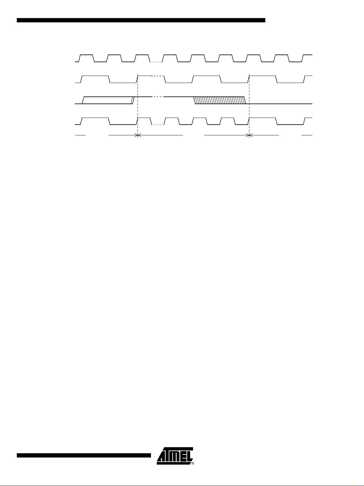
External Bus Cycles This section describes the bus cycles the T89C51CC01 executes to read (see
Figure 14), and write data (see Figure 15) in the external data memory.
External memory cycle takes 6 CPU clock periods. This is equivalent to 12 oscillator
clock period in standard mode or 6 oscillator clock periods in X2 mode. For further information on X2 mode.
Slow peripherals can be acc essed b y stretc hing th e read and write cycles . This is done
using the M0 bit in AUXR reg ister. S etting t his bi t changes the widt h of the RD
signals from 3 to 15 CPU clock periods.
For simplicity, the accompanying figures depict the bus cycle waveforms in idealized
form and do not provide precise timing information. For bus cycle timing parameters
refer to the Section “AC Characteristics”.
28
P3.6
and WR
4129L–CAN–08/05
Page 29
Figure 14. External Data Read Waveforms
CPU Clock
ALE
1
RD
A/T89C51CC01
P0
P2
Notes: 1. RD signal may be stretched using M0 bit in AUXR register.
2. When executing MOVX @Ri instr uction, P2 outputs SFR content.
P2
DPL or Ri D7:0
DPH or P22
Figure 15. External Data Write Waveforms
CPU Clock
ALE
WR1
P0
P2
P2
DPL or Ri D7:0
DPH or P22
4129L–CAN–08/05
Notes: 1. WR signal may be stretched using M0 bit in AUXR register.
2. When executing MOVX @Ri instr uction, P2 outputs SFR content.
29
Page 30
A/T89C51CC01
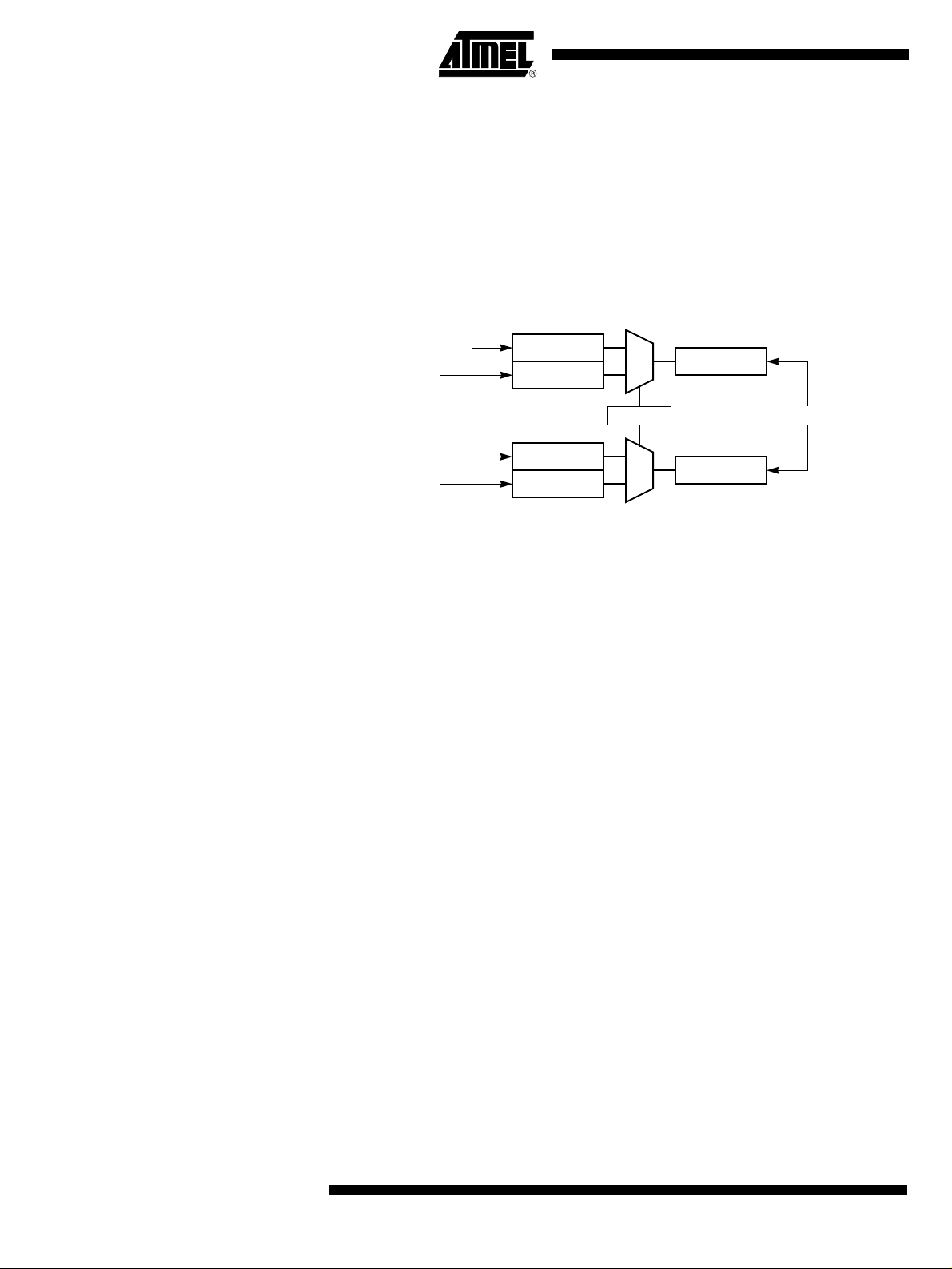
Dual Data Pointer
Description The T89C51CC01 implements a second data pointer for speedi ng up code execution
and reducing code size in case of intensive usage of external memory accesses.
DPTR 0 and DPTR 1 ar e seen b y the CPU as DPTR an d are acc essed using th e SFR
addresses 83h and 84h that are the DPH and DPL addresses. The DPS bit in AUXR1
register (see Figure 20) is used to select whether DPTR is the data pointer 0 or the data
pointer 1 (see Figure 16).
Figure 16. Dual Data Pointer Implementation
DPL0
DPL1
DPTR0
DPTR1
DPH0
DPH1
0
1
DPS
0
1
DPL
AUXR1.0
DPH
DPTR
Application Software can take advantage of the additional data pointers to both increase speed and
reduce code size, for example, block operations (copy, compare…) are well served by
using one data pointer as a “source” pointer and the other one as a “destination” pointer.
Hereafter is an example of block move implementation using the two pointers and coded
in assembler. The latest C compiler takes als o advantag e of this feature b y providin g
enhanced algorithm libraries.
The INC instruction is a short (2 Bytes) and fast (6 machine cycle) way to manipulate the
DPS bit in the AUXR 1 reg ister. H owever , note that th e INC i nstruc tion do es no t direc tly
force the DPS bit to a particular state, but simply toggles it. In simple routines, such as
the block move exa mple, o nly the f act that DP S is tog gled i n the pr oper s equenc e matters, not its actual value. In other words, the block move routine works the same whether
DPS is '0' or '1' on entry.
30
; ASCII block move using dual data pointers
; Modifies DPTR0, DPTR1, A and PSW
; Ends when encountering NULL character
; Note: DPS exits opposite to the entry state unless an extra INC AUXR1 is
added
AUXR1EQU0A2h
move:movDPTR,#SOURCE ; address of SOURCE
incAUXR1 ; switch data pointers
movDPTR,#DEST ; address of DEST
mv_loop:incAUXR1; switch data pointers
movxA,@DPTR; get a byte from SOURCE
incDPTR; increment SOURCE address
incAUXR1; switch data pointers
movx@DPTR,A; write the byte to DEST
incDPTR; increment DEST address
jnzmv_loop; check for NULL terminator
end_move:
4129L–CAN–08/05
Page 31

Registers Table 18. PSW Register
PSW (S:D0h)
Program Status Word Register
76543210
CY AC F0 RS1 RS0 OV F1 P
A/T89C51CC01
Bit
Number
7CY
6AC
5F0User Definable Flag 0.
4-3 RS1:0
2OV
1F1User Definable Flag 1
0P
Bit
Mnemonic Description
Carry Flag
Carry out from bit 1 of ALU operands.
Auxiliary Carry Flag
Carry out from bit 1 of addition operands.
Register Bank Select Bits
Refer to Table 16 for bits description.
Overflow Flag
Overflow set by arithmetic operations.
Parity Bit
Set when ACC contains an odd number of 1’s.
Cleared when ACC contains an even number of 1’s.
Reset Value = 0000 0000b
Table 19. AUXR Register
AUXR (S:8Eh)
Auxiliary Register
4129L–CAN–08/05
76543210
- - M0 - XRS1 XRS0 EXTRAM A0
Bit
Number
7-6 -
5M0
4-
3-2 XRS1-0
Bit
Mnemonic Description
Reserved
The value read from these bits are indeterminate. Do not set this bit.
Stretch MOVX control:
the RD/ and the WR/ pulse length is increased according to the value of M0.
M0
Pulse length in clock period
0 6
1 30
Reserved
The value read from this bit is indeterminate. Do not set this bit.
XRAM size:
Accessible size of the XRAM
XRS
1:0 XRAM size
0 0 256 Bytes
0 1 512 Bytes
1 0 768 Bytes
1 1 1024 Bytes (default)
31
Page 32

A/T89C51CC01
Bit
Number
1EXTRAM
0A0
Bit
Mnemonic Description
Internal/External RAM (00h - FFh)
access using MOVX @ Ri/@ DPTR
0 - Internal XRAM access using MOVX @ Ri/@ DPTR.
1 - External data memory access.
Disable/Enable ALE)
0 - ALE is emitted at a constant rate of 1/6 the oscillator frequency (or 1/3 if X2
mode is used)
1 - ALE is active only during a MOVX or MOVC instruction.
Reset Value = X00X 1100b
Not bit addressable
Table 20. AUXR1 Register
AUXR1 (S:A2h)
Auxiliary Control Register 1
76543210
- - ENBOOT - GF3 0 - DPS
Bit
Number
7-6 -
5ENBOOT
4-
3GF3General-purpose Flag 3
20
1-Reserved for Data Pointer Extension.
0DPS
Bit
Mnemonic Description
Reserved
The value read from these bits is indeterminate. Do not set these bits.
Enable Boot Flash
(1)
Set this bit for map the boot Flash between F800h -FFFFh
Clear this bit for disable boot Flash.
Reserved
The value read from this bit is indeterminate. Do not set this bit.
Always Zero
This bit is stuck to logic 0 to allow INC AUXR1 instruction without affecting GF3
flag.
Data Pointer Select Bit
Set to select second dual data pointer: DPTR1.
Clear to select first dual data pointer: DPTR0.
Reset Value = XXXX 00X0b
Note: 1. ENBOOT is initialized with the invert BLJB at reset. See In-System Programming
section.
32
4129L–CAN–08/05
Page 33

A/T89C51CC01
EEPROM Data Memory
Write Dat a i n the Column Latches
The 2-Kbyte on-chip EEPROM memory block is located at addresses 0000h to 07FFh of
the XRAM/XRAM memory space and is selected by setting control bits in the EECON
register. A read in the EEPROM memory is done with a MOVX instruction.
A physical write i n the E EPRO M memo ry is d one in two step s: write data in the co lumn
latches and transfer of all data latches into an EEPROM memory row (programming).
The number of data written on the page may vary from 1 up to 128 Bytes (the page
size). When programm ing, onl y the dat a writte n in the col umn latc h is pro grammed an d
a ninth bit is used to obtain this feature. This provides the capability to program the
whole memory by Bytes, by page or by a number of Bytes in a page. Indeed, each ninth
bit is set when the writing th e corresponding b yte in a row and all these n inth bits are
reset after the writing of the complete EEPROM row.
Data is written by byte to the column latches as for an external RAM memory. Out of the
11 address bits of t he d ata poi nter, the 4 MSBs are used fo r pag e s ele ct ion ( row ) and 7
are used for byte selection. Between tw o EEPROM programming sessions, all the
addresses in the column lat ches mus t stay on the sa me p age, mea ning tha t the 4 MSB
must no be changed.
The following procedure is used to write to the column latches:
• Save and disab le int erru pt.
• Set bit EEE of EECON register
• Load DPTR with the address to write
• Store A register with the data to be written
• Execute a MOVX @DPTR, A
• If needed loop the three last instructions until the end of a 128 Bytes page
• Restore interrupt.
Note: The last page address used when loading the column latch is the one used to select the
page programming address.
Programming The EEPROM programming consists of the following actions:
• writing one or more Bytes of one page in the column latches. Normally, all Bytes
must belong to the same page; if not, the last page address will be latched and the
others discarded.
• launching programming by writing the control sequence (50h followed by A0h) to the
EECON register.
• EEBUSY flag in EECON is then set by hardware to indicate that programming is in
progress and that the EEPROM segment is not available for reading.
• The end of programming is indicated by a hardware clear of the EEBUSY flag.
Note: The sequence 5xh and Axh must be executed without instructions between then other-
wise the programming is aborted.
Read Data The following procedure is used to read the data stored in the EEPROM memory:
• Save and disab le int er rupt
• Set bit EEE of EECON register
• Load DPTR with the address to read
• Execute a MOVX A, @DPTR
• Restore interrupt
4129L–CAN–08/05
33
Page 34

A/T89C51CC01
Examples ;*F*************************************************************************
;* NAME: api_rd_eeprom_byte
;* DPTR contain address to read.
;* Acc contain the reading value
;* NOTE: before execute this function, be sure the EEPROM is not BUSY
;***************************************************************************
api_rd_eeprom_byte:
; Save and clear EA
MOV EECON, #02h; map EEPROM in XRAM space
MOVX A, @DPTR
MOV EECON, #00h; unmap EEPROM
; Restore EA
ret
;*F*************************************************************************
;* NAME: api_ld_eeprom_cl
;* DPTR contain address to load
;* Acc contain value to load
;* NOTE: in this example we load only 1 byte, but it is possible upto
;* 128 Bytes.
;* before execute this function, be sure the EEPROM is not BUSY
;***************************************************************************
api_ld_eeprom_cl:
; Save and clear EA
MOV EECON, #02h ; map EEPROM in XRAM space
MOVX @DPTR, A
MOVEECON, #00h; unmap EEPROM
; Restore EA
ret
34
;*F*************************************************************************
;* NAME: api_wr_eeprom
;* NOTE: before execute this function, be sure the EEPROM is not BUSY
;***************************************************************************
api_wr_eeprom:
; Save and clear EA
MOV EECON, #050h
MOV EECON, #0A0h
; Restore EA
ret
4129L–CAN–08/05
Page 35

Registers Table 21. EECON Register
EECON (S:0D2h)
EEPROM Control Register
76543210
EEPL3 EEPL2 EEPL1 EEPL0 - - EEE EEBUSY
A/T89C51CC01
Bit Number
7-4 EEPL3-0
3-
2-
1EEE
0EEBUSY
Bit
Mnemonic Description
Programming Launch comma nd bits
Write 5Xh followed by AXh to EEPL to launch the programming.
Reserved
The value read from this bit is indeterminate. Do not set this bit.
Reserved
The value read from this bit is indeterminate. Do not set this bit.
Enable EEPROM Space bit
Set to map the EEPROM space during MOVX instructions (Write in the column
latches)
Clear to map the XRAM space during MOVX.
Programming Busy flag
Set by hardware when programming is in progress.
Cleared by hardware when programming is done.
Can not be set or cleared by software.
Reset Value = XXXX XX00b
Not bit addressable
4129L–CAN–08/05
35
Page 36

A/T89C51CC01
Program/Code Memory
The T89C51CC01 implement 32K Bytes of on -chip program /code memor y. Figure 17
shows the partitioning of internal and external program/code memory spaces depending
on the product.
The Flash memory increa ses EP ROM and ROM func tional ity by in-cir cui t electric al erasure and programming. Thanks to the internal charge pump, the high voltage needed for
programming or erasing Flash cells is generated on-chip using the standard VDD voltage. Thus, the Flash Memory can be programmed using only one voltage and allows InSystem-Programming commonly known as ISP. Hardware programming mode is also
available using specific programming tool.
Figure 17. Program/Code Memory Organization
FFFFh
32K Bytes
external
memory
8000h
7FFFh
7FFFh
32K Bytes
internal
Flash
EA = 1
0000h
Notes: 1. If the program executes exclus ively from on-chip code memory (not from external
memory), beware of executing code from the upper byte of on-chip memory (7FFFh)
and thereby disrupt I/O Ports 0 and 2 due to external prefetch. Fetching code constant from this location does not affect Ports 0 and 2.
2. Default factory programmed parts come with maximum hardware protection. Execution from external memory is not possible unless the Hardware Security Byte is
reprogrammed. See Table 27.
0000h
32K Bytes
external
memory
EA = 0
36
4129L–CAN–08/05
Page 37

A/T89C51CC01
17.22 External Code Memory Access
Memory Interfac e The external memory interface comprises the external bus (port 0 and port 2) as well as
the bus control signals (PSEN#, and ALE).
Figure 18 shows the structure of the external address bus. P0 carries address A7:0
while P2 carries address A15:8. Data D7:0 is multiplexed with A7:0 on P0. Table 18
describes the external memory interface signals.
Figure 18. External Code Memory Interface Structure
T89C51CC01
AD7:0
A15:8
Latch
A7:0
P2
ALE
P0
Table 23. External Code Memory Interface Signals
Signal
Name Type Description
A15:8 O
AD7:0 I/O
ALE O
PSEN# O
Address Lines
Upper address lines for the external bus.
Address/Data Lines
Multiplexed lower address lines and data for the external memory.
Address Latch Enable
ALE signals indicates that valid address information are available on lines
AD7:0.
Program Store Enable Output
This signal is active low during external code fetch or external code read
(MOVC instruction).
Flash
EPROM
A15:8
A7:0
D7:0
OEPSEN#
Alternate
Function
P2.7:0
P0.7:0
-
-
External Bus Cycles This section describes the bus cycles the T89C51CC01 executes to fetch code (see
Figure 19) in the external program/code memory.
External memory cycle takes 6 CPU clock periods. This is equivalent to 12 oscillator
clock period in standard mode or 6 oscillator clock periods in X2 mode. For further information on X2 mode see section “Clock “.
For simplicity, the accompanying figure depicts the bus cycle waveforms in idealized
form and do not provide precise timing information.
For bus cycling parameters refer to the ‘AC-DC parameters’ section.
37
4129L–CAN–08/05
Page 38

A/T89C51CC01
Figure 19. External Code Fetch Waveforms
CPU Clock
ALE
PSEN#
D7:0
P0
P2
Flash Memory Architecture
T89C51CC01 features two on-chip Flash memories:
•Flash memory FM0:
•Flash memory FM1:
The FM0 can be pr og ram by both parallel progra mmi ng and S eria l In - Syst em- Pro gr amming (ISP) whereas FM1 suppor ts only par al lel pro gr am min g by prog ra mme rs. T he ISP
mode is detailed in the "In-System-Programming" section.
All Read/Write access operations on Flash Memory by user application are managed by
a set of API described in the "In-System-Programming" section.
Figure 20. Flash Memory Architecture
Hardware Security (1 byte)
Extra Row (128 Bytes)
Column Latches (128 Bytes)
PCL
PCHPCH
PCLD7:0 D7:0
PCH
containing 32K Bytes of program memory (user space) organized into 128 byte
pages,
2K Bytes for boot loader and Application Programming Interfaces (API).
2K Bytes
Flash mem ory
boot space
FM1
FFFFh
F800h
38
7FFFh
0000h
32K Bytes
Flash mem ory
user space
FM0
FM1 mapped between F800h and
FFFFh when bit ENBOOT is set in
AUXR1 register
4129L–CAN–08/05
Page 39

A/T89C51CC01
FM0 Memory Architecture The Flash memory is made up of 4 blocks (see Figure 20):
• The memory array (user space) 32K Bytes
• The Extra Row
• The Hardware security bits
• The column latch registers
User Space This space is composed of a 32K Bytes Flash memory organized in 256 pages of 128
Bytes. It contains the user’s application code.
Extra Row (XRow) This row is a part of FM0 and has a size of 128 Bytes . The ex tra r ow may c on tai n info r-
mation for boot loader usage.
Hardware Security Byte The Hardware security Byte space is a part of FM0 and has a size of 1 byte.
The 4 MSB can be read/written by software, the 4 LSB can only be read by software and
written by hardware in parallel mode.
Column Latches The column latches, also part of FM0, have a size of full page (128 Bytes).
The column latches are the entrance buffers of the three previous memory locations
(user array, XROW and Hardware security byte).
Cross Flash Memory Access
Description
The FM0 memory can be program only f rom FM 1. Prog ra mmi ng FM0 fr om FM0 or from
external memory is impossible.
The FM1 memory can be program only by parallel programming.
The Table 24 show all software Flash access allowed.
Table 24. Cross Flash Memory Access
(user Flash)
(boot Flash)
Code executing from
FM0
FM1
External
memory
EA = 0
Action
Read ok -
Load column latch ok -
Write - Read ok ok
Load column latch ok -
Write ok Read - -
Load column latch - -
Write - -
FM0
(user Flash)
FM1
(boot Flash)
4129L–CAN–08/05
39
Page 40

A/T89C51CC01
Overview of FM0 Operations
The CPU interfaces to the Flash memor y through the FCON register and AUX R1
register.
These registers are used to:
• Map the memory spaces in the adressable space
• Launch the programming of the memory spaces
• Get the status of the Flash memory (busy/not busy)
Mapping of the Memory Space By default, the user space is accessed by MOVC instruction for read only. The column
latches space is made accessible by setting the FPS bit in FCON register. Writing is
possible from 0000h to 7FFFh, address bits 6 to 0 are used to select an address within a
page while bits 14 to 7 are used to select the programming address of the page.
Setting FPS bit takes precedence on the EXTRAM bit in AUXR register.
The other memory spaces (user, extra row, hardware security) are made accessible in
the code segment by programming bits FMOD0 and FMOD1 in FCON register in accordance with Table 25. A MOVC instruction is then used for reading these spaces.
Table 25. FM0 Blocks Select Bits
FMOD1 FMOD0 FM0 Adressab le space
0 0 User (0000h-7FFFh)
0 1 Extra Row(FF80h-FFFFh)
1 0 Hardware Security Byte (0000h)
11Reserved
Launching Programming FPL3:0 bits in FCO N regist er are us ed to s ecure th e launc h of pr ogrammi ng. A s pecific
sequence must be written in these bits to unlock the write protection and to launch the
programming. This sequence is 5xh followed by Axh. Table 26 summarizes the memory
spaces to program according to FMOD1:0 bits.
40
4129L–CAN–08/05
Page 41

Table 26. Programming Spaces
Write to FCON
5 X 0 0 No action
A/T89C51CC01
OperationFPL3:0 FPS FMOD1 FMOD0
User
Extra Row
Hardware
Security
Byte
Reserved
Notes: 1. The sequence 5xh and Axh must be executing without instructions between them
2. Interrupts that may occur during programming time must be disabled to avoid any
AX00
5 X 0 1 No action
AX01
5 X 1 0 No action
A X 1 0 Write the fuse bits space
5 X 1 1 No action
A X 1 1 No action
otherwise the programming is aborted.
spurious exit of the programming mode.
Write the column latches in user
space
Write the column latches in extra row
space
Status of the Flash Memory The bit FBUSY in FCON register is used to indicate the status of programming.
FBUSY is set when programming is in progress.
Selecting FM1 The bit ENBOOT in AUXR1 register is used to map FM1 from F800h to FFFFh.
Loading the Column Latches Any number of data from 1 Byte to 12 8 By tes can be loa ded in the colu mn l atc hes . This
provides the capability to program the whole memory by byte, by page or by any number
of Bytes in a page.
When progra mmin g is laun ched, a n aut omati c erase of the loc atio ns load ed in th e col umn latches is first performed, then programming is effectively done. Thus no page or
block erase is needed and only the loaded data are programmed in the corresponding
page.
4129L–CAN–08/05
The following procedure is used to load the column latches and is summarized in
Figure 21:
• Save then disable interrupt and map the column latch space by setting FPS bit.
• Load the DPTR with the address to load.
• Load Accumulator register with the data to load.
• Execute the MOVX @DPTR, A instruction.
• If needed loop the three last instructions until the page is completely loaded.
• Unmap the column latch and Restore Interrupt
41
Page 42

A/T89C51CC01
Figure 21. Column Latches Loading Procedure
Column Latches
Loading
Save and Disable IT
EA = 0
Column Latches Mapping
FCON = 08h (FPS=1)
Data Load
DPTR = Ad dress
ACC = Data
Exec: MOVX @DPTR, A
Last Byte
to load?
Data memory Mapping
FCON = 00h (FPS = 0)
Restore IT
Note: The last page address used when loading the column latch is the one used to select the
page programming address.
Programming the Flash Spaces
User The following procedure is used to program the User space and is summarized in
Figure 22:
• Load up to one page of data in the column latches from address 0000h to 7FFFh.
• Save then disable the interrupts.
• Launch the programming by writing the data sequence 50h followed by A0h in
FCON register (only from FM1).
The end of the programming indicated by the FBUSY flag cleared.
• Restore the interrupts.
Extra Row The following procedure is used to pr ogra m the Extra Row space a nd is summ arized i n
Figure 22:
• Load data in the column latches from address FF80h to FFFFh.
• Save then disable the interrupts.
• Launch the programming by writing the data sequence 52h followed by A2h in
FCON register. This step of the procedure must be executed from FM1. The end of
the programming indicated by the FBUSY flag cleared.
The end of the programming indicated by the FBUSY flag cleared.
• Restore the interrupts.
42
4129L–CAN–08/05
Page 43
Figure 22. Flash and Extra Row Programming Procedure
Flash Spaces
Programming
Column Latches Loading
see Figure 21
Save and Disable IT
EA = 0
Launch Programming
FCON = 5xh
FCON = Axh
FBusy
Cleared?
A/T89C51CC01
Hardware Security Byte
Clear Mode
FCON = 00h
End Programming
Restore IT
The following procedure is used to program the Hardware Sec urity Byte space
and is summarized in Figure 23:
• Set FPS and map Hardware byte (FCON = 0x0C)
• Save and disab le the interru pts.
• Load DPTR at address 0000h.
• Load Accumulator register with the data to load.
• Execute the MOVX @DPTR, A instruction.
• Launch the programming by writing the data sequence 54h followed by A4h in
FCON register. This step of the procedure must be executed from FM1. The end of
the programming indicated by the FBUSY flag cleared.
The end of the programming indicated by the FBusy flag cleared.
• Restore the interrupts.
4129L–CAN–08/05
43
Page 44

A/T89C51CC01
Figure 23. Hardware Programming Procedure
Flash Spaces
Programming
Save and Disable IT
EA = 0
FCON = 0Ch
Save and Disable IT
EA = 0
Launch Programming
FCON = 54h
FCON = A4h
Data Load
DPTR = 00h
ACC = Data
Exec: MOVX @DPTR, A
End Loading
Restore IT
FBusy
Cleared?
Clear Mode
FCON = 00h
End Programming
RestoreIT
Reading the Flash Spaces
User The following procedure is used to read the User space:
• Read one byte in Accumulator by executing MOVC A,@A+DPTR where A+DPTR is
the address of the code byte to read.
Note: FCON is supposed to be reset when not needed.
Extra Row The following procedure is used to read the Extra Row space and is summarized in
Figure 24:
• Map the Extra Row space by writing 02h in FCON register.
• Read one byte in Accumulator by executing MOVC A,@A+DPTR with A = 0 and
DPTR = FF80h to FFFFh.
• Clear FCON to unmap the Extra Row.
Hardware Security Byte
44
The following procedure is used to read the Hardware Security space and is
summarized in Figure 24:
• Map the Hardware Security space by writing 04h in FCON register.
• Read the byte in Accumulator by executing MOVC A,@A+DPTR with A = 0 and
DPTR = 0000h.
• Clear FCON to unmap the Hardware Security Byte.
4129L–CAN–08/05
Page 45
Figure 24. Reading Procedure
A/T89C51CC01
Flash Spaces Reading
Flash Protection from Parallel
Programming
Flash Spaces Mapping
FCON = 0000aa0b
Data Read
DPTR = Address
ACC = 0
Exec: MOVC A, @A+DPTR
Clear Mode
FCON = 00h
(1)
Note: 1. aa = 10 for the Hardware Security Byte.
The three lock bits in Hardware Security Byte (see "In-System-Programming" section)
are programmed according to Table 27 provide different level of protection for the onchip code and data located in FM0 and FM1.
The only way to write these bits are the parallel mode. They are set by default to level 4
Table 27. Program Lock bit
Program Lock Bits
Security
Level
1 UUU
2PUU
3UPU
4UUP
LB0 LB1 LB2
Protection Description
No program lock features enabled. MOVC instruction executed from
external program memory returns non coded data.
MOVC instructions executed from external program memory are barred
to return code bytes from internal memory, EA
on reset, and further parallel programming of the Flash is disabled.
Same as 2, also verify through parallel programming interface is
disabled.
Same as 3, also external execution is disabled if code roll over beyond
7FFFh
Program Lock bits
U: unprogrammed
P: programmed
WARNING: Security level 2 and 3 should only be programmed after Flash and Core
verification.
Preventing Flash Corruption See the “Power Management” section.
is sampled and latched
4129L–CAN–08/05
45
Page 46

A/T89C51CC01
Registers FCON RegisterFCON (S:D1h)
Flash Control Register
76543210
FPL3 FPL2 FPL1 FPL0 FPS FMOD1 FMOD0 FBUSY
Bit
Number
7-4 FPL3:0
3FPS
2-1 FMOD1:0
0FBUSY
Bit
Mnemonic Description
Programming Launch Command Bits
Write 5Xh followed by AXh to launch the programming according to FMOD1:0
(see Table 26)
Flash Map Program Space
Set to map the column latch space in the data memory space.
Clear to re-map the data memory space.
Flash Mode
See Table 25 or Table26.
Flash Busy
Set by hardware when programming is in progress.
Clear by hardware when programming is done.
Can not be changed by software.
Reset Value = 0000 0000b
46
4129L–CAN–08/05
Page 47

A/T89C51CC01
4129L–CAN–08/05
47
Page 48

A/T89C51CC01
Operation Cross Memory Access
Table 28. Cross Memory Access
Space addressable in read and write are:
•RAM
• ERAM (Expanded RAM access by movx)
• XRAM (eXternal RAM)
• EEPROM DATA
• FM0 (user flash)
• Hardware byte
•XROW
•Boot Flash
• Flash Column latch
The table below provide the different kind of memory which can be accessed from different code location.
Action RAM
boot FLASH
FM0
External
memory
EA = 0
or Code Roll
Over
Read OK OK OK OK Write - OK
Read - OK OK OK Write - OK (idle) OK
Read - - OK - -
Write - - OK
Note: 1. RWW: Read While Write
XRAM
ERAM Boot FLASH FM0 E² Data
(1)
OK
(1)
(1)
(1)
Hardware
Byte XROW
(1)
OK
-OK
--
OK
(1)
48
4129L–CAN–08/05
Page 49

Sharing Instructions Table 29. Instr uct ions shared
A/T89C51CC01
XRAM
Action RAM
Read MOV MOVX MOVX MOVC MOVC MOVC MOVC
Write MOV MOVX MOVX - by cl by cl by cl
ERAM
EEPROM
DATA
Boot
FLASH FM0
Hardware
Byte XROW
Note: by cl: using Column Latch
Table 30. Read MOVX A, @DPTR
EEE bit in
EECON
Register
00XXOK
01XXOK
10XX OK
11XXOK
FPS in
FCON Register ENBOOT EA
XRAM
ERAM
EEPROM
DATA
Table 31. Write MOVX @DPTR,A
EEE bit in
EECON
Register
FPS bit in
FCON Register ENBOOT EA
XRAM
ERAM
EEPROM
Data
Flash
Column
Latch
Flash
Column
Latch
00XXOK
01X
10XX OK
11X
1OK
0OK
1OK
0OK
4129L–CAN–08/05
49
Page 50

A/T89C51CC01
T able 32. Read MOVC A, @DPTR
Code Execution
From FM0
From FM1
(ENBOOT =1
FCON Register
ENBOOT DPTR FM1 FM0 XROW
0 0000h to 7FFFh OK
00X
01X X
10X X X OK
11X
0
00
1
01X
1
0 000h to 7FFFh OK
1
1
0X NA
1X OK
0X NA
1
0NA
0000h to 7FFFh OK
F800h to FFFFh Do not use this configuration
0000 to 007Fh
(1)
See
0000h to 7FFFh OK
F800h to FFFFh Do not use this configuration
0000h to 7FFF OK
F800h to FFFFh OK
0000h to 007h
(2)
See
OK
OK
Hardware
Byte
External
CodeFMOD1 FMOD0 FPS
External code:
EA=0 or Code
Roll Over
10X
11X
X0X X X OK
1
0NA
1
0NA
X
OK
000h to 7FFFh
OK
1. For DPTR higher than 007Fh only lowest 7 bits are decoded, thus the behavior is the same as for addresses from 0000h to
007Fh
2. For DPTR higher than 007Fh only lowest 7 bits are decoded, thus the behavior is the same as for addresses from 0000h to
007Fh
50
4129L–CAN–08/05
Page 51

A/T89C51CC01
h
In-System Programming (ISP)
Flash Programming and Erasure
With the implementation of the User Space (FM0) and the Boot Space (FM1) in Flash
technology the T89C51CC01 allows the system engineer the development of applications with a very high l evel of flex ibility . Th is fle xibili ty is based on the p ossibi lity t o alter
the customer program at any stages of a product’s life:
• Before mounting the chip on the PCB, FM0 Flash can be programmed with the
application code. FM1 is always pre programmed by Atmel with a bootloader (chip
can be ordered with CAN bootloader or UART bootloader).
• Once the chip is mounted on the PCB, it can be programmed by serial mode via the
CAN bus or UART.
Note: 1. The user can also program his own bootloader in FM1.
This In-System-Programming (ISP) allows code modification over the total lifetime of the
product.
Besides the default Boot loader Atmel provide to the customer also all the needed Application-Programming-Interfaces (API) which are needed for the ISP. The API are located
also in the Boot memory.
This allow the customer to have a full use of the 32-Kbyte user memory.
There are three methods of programming the Flash memory:
• The Atmel bootloader located in FM1 is activated by the application. Low level API
routines (located in FM1)will be used to program FM0. The interface used for serial
downloading to FM0 is the UART or the CAN. API can be called also by the user’s
bootloader located in FM0 at [SBV]00h.
• A further method exists in activating the Atmel boot loader by hardware activation.
See Section “Hardware Security Byte”.
• The FM0 can be programmed also by the parallel mode using a programmer.
(1)
Figure 25. Flash Memory Mapping
7FFFh
Custom
Boot Loader
[SBV]00h
32K Bytes
Flash memory
FM0
0000h
F800h
FFFFh
2K Bytes IAP
bootloader
FM1
FM1 mapped between F800h and FFFF
when API called
4129L–CAN–08/05
51
Page 52

A/T89C51CC01
Boot Process
Software Boot Proc ess
Example
Many algorithms can be used for the software boot process. Below are descriptions of
the different flags and Bytes.
Boot Loader Jump Bit (BLJB):
- This bit indicate s if on RESET the us er wants to jum p to this applic ation at addr ess
@0000h on FM0 or execute the boot loader at address @F800h on FM1.
- BLJB = 0 (i.e. boo tloader FM 1 execut ed after a res et) is t he d efault Atm el fac tory pr o-
gramming.
- To read or modify this bit, the APIs are used.
Boot Vector Address (SBV):
- This byte contains the MSB of the user boot loader address in FM0.
- The default value of SBV is FFh (no user boot loader in FM0).
- To read or modify this byte, the APIs are used.
Extra Byte (EB) and Boot Status Byte (BSB):
- These Bytes are reserved for customer use.
- To read or modify these Bytes, the APIs are used.
Hardware Boot Process At the falling edge of RESET, the bit ENBOOT in AUXR1 register is initialized with the
value of Boot Loader Jump Bit (BLJB).
Further at the fa lling edge of RE SET i f the follow ing c ondition s ( called Hardwa re cond i-
tion) are detected. The FCON register is initialized with the value 00h and the PC is
initialized with F800h (FM1 lower byte = Bootloader entry point).
Hardware Conditions:
• PSEN low
(1)
• EA high,
• ALE high (or not connec ted ).
The Hardware condi tion forces the bootl oader to b e exec uted, w hatev er B LJB v alue is.
Then BLBJ will be checked.
If no hardware cond iti on is d etec te d, t he F C ON r egiste r is i ni tia li ze d wi th the v alu e F0 h.
Then BLJB value will be checked.
Conditions are:
• If bit BLJB = 1:
User application in FM0 will be started at @0000h (standard reset).
• If bit BLJB = 0:
Boot loader will be started at @F800h in FM1.
Note: 1. As PSEN is an output port in normal operating mode (running user applications or
bootloader applications) after reset it is recommended to release PSEN after the falling edge of Reset is signaled.
The hardware conditions are sampled at reset signal Falling Edge, thus they can be
released at any time when reset input is low.
2. To ensure correct microcontroller startup, the PSEN pin should not be tied to ground
during power-on.
52
4129L–CAN–08/05
Page 53

Figure 26. Hardware Boot Process Algorithm
t,
A/T89C51CC01
Hardware
ENBOOT = 0
PC = 0000h
No
RESET
Hardware
condition?
No
BLJB = = 0
?
Yes
ENBOOT = 1
PC = F800h
bit ENBOOT in AUXR1 register
is initialized with BLJB inverted.
(Example, if BLJB=0, ENBOOT is set (=1) during rese
thus the bootloader is executed after the reset)
ENBOOT = 1
PC = F800h
FCON = 00h
Yes
FCON = F0h
Application
in FM0
Boot Loader
in FM1
Software
Application Programming Interface
Several Application Program Interface (API) calls are available for use by an application
program to permit selective erasing and programming of Flash pages. All calls are made
by functions.
All of these APIs are desc ribed in detail in the following documents on the Atmel web
site.
• Datasheet Bootloader CAN T89C51CC01
• Datasheet Bootloader UART T89C51CC01
XROW Bytes Table 33. XROW Mapping
Description Default Value A dd ress
Copy of the Manufacturer Code 58h 30h
Copy of the Device ID#1: Family code D7h 31h
Copy of the Device ID#2: Memories size and type F7h 60h
Copy of the Device ID#3: Name and Revision FFh 61h
4129L–CAN–08/05
53
Page 54

A/T89C51CC01
Hardware Security Byte Table 34. Hardware Security Byte
76543210
X2B BLJB - - - LB2 LB1 LB0
Bit
Number
7X2B
6BLJB
5-3 -
2-0 LB2:0 Lock Bits
Bit
Mnemonic Description
X2 Bit
Set this bit to start in standard mode.
Clear this bit to start in X2 mode.
Boot Loader JumpBit
- 1: To start the user’s application on next RESET (@0000h) located in FM0,
- 0: To start the boot loader(@F800h) located in FM1.
Reserved
The value read from these bits are indeterminate.
Default value after erasing chip: FFh
Notes: 1. Only the 4 MSB bits can be accessed by software.
2. The 4 LSB bits can only be accessed by parallel mode.
54
4129L–CAN–08/05
Page 55

A/T89C51CC01
Serial I/O Port The T89C51CC01 I/O serial port is compatible with the I/O serial port in the 80C52.
It provides both synchronous and asynchronous communication modes. It operates as a
Universal Asynchronous Receiver and Transmitter (UART) in three full-dup lex modes
(Modes 1, 2 and 3). Asynchronous transmission and reception can occur simultaneously
and at different baud rates
Serial I/O port includes the following enhancements:
• Framing error detection
• Automatic address recognition
Figure 27. Serial I/O Port Block Diagram
IB Bus
TXD
RXD
SBUF
Transmitter
Write SBUF
Mode 0 Transmit
RI
TI
SBUF
Receiver
Receive
Shift register
Read SBUF
Load SBUF
Serial Port
Interrupt Request
Framing Error Detection Framing bit error detection is provided for the three asynchronous modes. To enable the
framing bit error detection feature, set SMOD0 bit in PCON register.
Figure 28. Framing Error Block Diagram
RITIRB8TB8RENSM2SM1SM0/FE
Set FE bit if stop bit is 0 (framing error)
4129L–CAN–08/05
SM0 to UART mode control
IDLPDGF0GF1POF-SMOD0SMOD1
To UART framing error control
When this feature is enabled, the receiver checks each incoming data frame for a valid
stop bit. An invalid stop bit may result from noise on the serial lines or from simultaneous
transmission by two CPUs. If a valid stop bit is not found, the Framing Error bit (FE) in
SCON register bit is set.
The software may examine the FE bit after ea ch reception to ch eck for data errors.
Once set, only softwa r e o r a r es et clea rs t he FE b it. Subsequently received fr am es with
valid stop bits cannot clear the FE bit. When the FE feature is enabled, RI rises on the
stop bit instead of the last data bit (See Figure 29. and Figure 30.).
55
Page 56

A/T89C51CC01
Figure 29. UART Timing in Mode 1
Automatic Address Recognition
RXD
RI
SMOD0=X
FE
SMOD0=1
Start
bit
Data byte
D7D6D5D4D3D2D1D0
Stop
bit
Figure 30. UART Timing in Modes 2 and 3
RXD
RI
SMOD0=0
RI
SMOD0=1
FE
SMOD0=1
Start
bit
Data byte Ninth
D8D7D6D5D4D3D2D1D0
Stop
bit
bit
The automatic addr es s rec ogn iti on feat ur e i s en abl ed when the multiprocess or c om munication feature is enabled (SM2 bit in SCON register is set).
Implemented in the hardware, automatic address recognition enhances the multiprocessor communication feature by allowing the serial port to examine the address of each
incoming command frame. Only when the serial port recognizes its own address will the
receiver set the RI bit in the SCON register to generate an interrupt. This ensures that
the CPU is not interrupted by command frames addressed to other devices.
56
If necessary, you ca n enable the automatic ad dress rec ognition feature in mode 1. In
this configuration, the stop bit takes the place of the ninth data bit. Bit RI is set only when
the received command frame address matches the device’s address and is terminated
by a valid stop bit.
To support automatic a ddr ess re co gni tio n, a dev ic e i s identified by a given add re ss an d
a broadcast address.
Note: The multiprocessor communication and automatic address recognition features cannot
be enabled in mode 0 (i.e. setting SM2 bit in SCON register in mode 0 has no effect).
4129L–CAN–08/05
Page 57

A/T89C51CC01
Given Address Each device has an individual address that is specified in the SADD R register; the
SADEN register is a mask byte that contains don’t-care bits (defined by zeros) to form
the device’s given address. T he don’t-care bits provide the flexibility to address one or
more slaves at a time. The following example illustrates how a given address is formed.
To address a device by its individual address, the SADEN mask byte must be 1111
1111b.
For example:
SADDR0101 0110b
1111 1100b
SADEN
Given0101 01XXb
Here is an example of how to use given addresses to address different slaves:
Slave A:SADDR1111 0001b
Slave B:SADDR1111 0011b
1111 1010b
SADEN
Given1111 0X0Xb
SADEN
1111 1001b
Given1111 0XX1b
Slave C:SADDR1111 0011b
1111 1101b
SADEN
Given1111 00X1b
The SADEN byte is selected so that each slave may be addressed separately.
For slave A, bit 0 (the LSB) is a don’t-care bit; for slaves B and C, bit 0 is a 1. To communicate with sl ave A onl y, the ma ster mus t send an ad dres s where bi t 0 is clea r (e.g.
1111 0000b).
For slave A, bit 1 is a 0; for slaves B and C, bit 1 is a don’t care bit. To communicate with
slaves A and B, but not slave C, the master must send an address with bits 0 and 1 both
set (e.g. 1111 0011b).
To communicate with slaves A, B and C, the master must send an address with bit 0 set,
bit 1 clear, and bit 2 clear (e.g. 1111 0001b).
Broadcast Address A broadcast address is formed from the logical OR of the SADDR and SADEN registers
with zeros defined as don’t-care bits, e.g.:
SADDR 0101 0110b
SADEN 1111 1100b
SADDR OR SADEN1111 111Xb
The use of don’t-care bits provides flexibility in defining the broadcast address, however
in most applications, a broadcast address is FFh. The following is an example of using
broadcast addresses:
Slave A:SADDR1111 0001b
1111 1010b
SADEN
Given1111 1X11b,
4129L–CAN–08/05
Slave B:SADDR1111 0011b
SADEN
1111 1001b
Given1111 1X11B,
Slave C:SADDR=1111 0010b
1111 1101b
SADEN
Given1111 1111b
57
Page 58

A/T89C51CC01
For slaves A and B, bit 2 is a don’t care bit; for slave C, bit 2 is set. To communicate with
all of the slaves, the ma ster must se nd an add ress F Fh. To c ommun icate with sl aves A
and B, but not slave C, the master can send and address FBh.
Registers Table 35. SCON Register
SCON (S:98h)
Serial Control Register
76543210
FE/SM0 SM1 SM2 REN TB8 RB8 TI RI
Bit
Number
7
6SM1
5SM2
4REN
3TB8
2RB8
Bit
Mnemonic Description
FE
SM0
Framing Error bit (S MOD0=1)
Clear to reset the error state, not cleared by a valid stop bit.
Set by hardware when an invalid stop bit is detected.
Serial port Mode bit 0 (SMOD0=0)
Refer to SM1 for serial port mode selection.
Serial port Mode bit 1
SM1 Mode Baud Rate
SM0
0 0 Shift Register F
0 1 8-bit UART Variable
1 0 9-bit UART F
1 1 9-bit UART Variable
Serial port Mode 2 bit/Multiprocessor Communication Enable bit
Clear to disable multiprocessor communication feature.
Set to enable multiprocessor communication feature in mode 2 and 3.
Reception Enable bit
Clear to disable serial reception.
Set to enable serial reception.
Transmitter Bit 8/Ninth bit to transmit in modes 2 and 3
Clear to transmit a logic 0 in the 9th bit.
Set to transmit a logic 1 in the 9th bit.
Receiver Bit 8/Ninth bit received in modes 2 and 3
Cleared by hardware if 9th bit received is a logic 0.
Set by hardware if 9th bit received is a logic 1.
XTAL
XTAL
/12 (or F
/64 or F
/6 in mode X2)
XTAL
/32
XTAL
58
Transmit Interrupt flag
1TI
0RI
Clear to acknowledge interrupt.
Set by hardware at the end of the 8th bit time in mode 0 or at the beginning of the
stop bit in the other modes.
Receive Interrupt flag
Clear to acknowledge interrupt.
Set by hardware at the end of the 8th bit time in mode 0, see Figure 29. and
Figure 30. in the other modes.
Reset Value = 0000 0000b
Bit addressable
4129L–CAN–08/05
Page 59

A/T89C51CC01
Table 36. SA DEN Regist er
SADEN (S:B9h)
Slave Address Mask Register
76543210
––––––––
Bit
Number
7-0 Mask Data for Slave Individual Address
Bit
Mnemonic Description
Reset Value = 0000 0000b
Not bit addressable
Table 37. SADDR Register
SADDR (S:A9h)
Slave Address Register
76543210
––––––––
Bit
Number
7-0 Slave Individual Address
Bit
Mnemonic Description
Reset Value = 0000 0000b
Not bit addressable
Table 38. SBUF Register
4129L–CAN–08/05
SBUF (S:99h)
Serial Data Buffer
76543210
––––––––
Bit
Number
7-0 Data sent/received by Serial I/O Port
Bit
Mnemonic Description
Reset Value = 0000 0000b
Not bit addressable
59
Page 60

A/T89C51CC01
Table 39. PCON Register
PCON (S:87h)
Power Control Register
76543210
SMOD1 SMOD0 – POF GF1 GF0 PD IDL
Bit
Number
7SMOD1
6SMOD0
5-
4POF
3GF1
2GF0
1PD
0IDL
Bit
Mnemonic Description
Serial port Mode bit 1
Set to select double baud rate in mode 1, 2 or 3.
Serial port Mode bit 0
Clear to select SM0 bit in SCON register.
Set to select FE bit in SCON register.
Reserved
The value read from this bit is indeterminate. Do not set this bit.
Power-Off Flag
Clear to recognize next reset type.
Set by hardware when VCC rises from 0 to its nominal voltage. Can also be set
by software.
General-purpose Flag
Cleared by user for general-purpose usage.
Set by user for general-purpose usage.
General-purpose Flag
Cleared by user for general-purpose usage.
Set by user for general-purpose usage.
Power-Down mode bit
Cleared by hardware when reset occurs.
Set to enter power-down mode.
Idle mode bit
Clear by hardware when interrupt or reset occurs.
Set to enter idle mode.
60
Reset Value = 00X1 0000b
Not bit addressable
4129L–CAN–08/05
Page 61

A/T89C51CC01
Timers/Counters The T89C51CC01 implemen ts two general-purpose, 16-bit Timers/Counters. Such are
identified as Timer 0 and Timer 1, and can be independentl y configu red to opera te in a
variety of modes as a Timer or an event Counter. When operating as a Timer, the
Timer/Counter runs for a programmed length of time, then issues an interrupt request.
When operating as a Counter, the Tim er/Counter counts n egative transit ions on an
external pin. After a preset number of counts, the Counter issues an interrupt request.
The various o perating modes o f each Ti mer/Count er are de scribed in the fo llowing
sections.
Timer/Counter Operations
A basic operation is Timer registers THx and TLx (x = 0, 1) connected in cascade to
form a 16-bit Timer. Setting the run control bit (TRx) in TCON register (see Figure 40)
turns the Timer on by allowing the selected input to increment TLx. When TLx overflows
it increments THx; when T Hx overflows it sets the T imer overflow f lag (TFx) in T CON
register. Setting the TRx does not clear the THx and TLx Timer registers. Timer registers can be accessed to obtain the cur rent co unt or to enter pr eset value s. They ca n be
read at any time but TRx bit must be cleared to preset their values, otherwise the behavior of the Timer/Counter is unpredictable.
The C/Tx# control bit selects Timer operation or Counter operation by selecting the
divided-down peripheral clock or external pin T x as the source for the counted signal.
TRx bit must be cleared when changing the mode of operation, otherwise the behavior
of the Timer/Counter is unpredictable.
For Timer op erat ion (C/Tx # = 0 ), t he T ime r reg ist er co unts the divid ed-d own peri phera l
clock. The Timer register is incremented once every peripheral cycle (6 peripheral clock
periods). The Tim er clo ck rate i s F
PER
/6, i.e. F
/12 in standard mode or F
OSC
OSC
/6 in X2
mode.
For Counter operation (C/Tx # = 1), the T im er reg ister cou nts the neg ati ve tran si ti ons on
the Tx external input pin. The ex ternal input is sampled every peripheral cycles. When
the sample is high in one cycle and low in the next one, the Counter is incremented.
Since it takes 2 cycles (12 peripheral clock periods) to recognize a negative transition,
the maximum count rate is F
/12, i.e. F
PER
/24 in standard mode or F
OSC
/12 in X2
OSC
mode. There are no restrictions on the duty cycle of the external input signal, but to
ensure that a given level is sampled at least once before it changes, it should be held for
at least one full peripheral cycle.
Timer 0 Timer 0 functions as either a Timer or event Counter in four modes of operation.
Figure 31 to Figure 34 show the logical configuration of each mode.
Timer 0 is controlled by th e four l ower bits of TMOD re gister (s ee Figur e 41) and bits 0,
1, 4 and 5 of TCON register (see Figure 40). TMOD register selects the method of Timer
gating (GATE0), Timer or Counter operation (T/C0#) and mode of operation (M10 and
M00). TCON register provides Timer 0 control functions: overflow flag (TF0), run control
bit (TR0), interrupt flag (IE0) and interrupt type control bit (IT0).
For normal Timer ope ratio n (GAT E0 = 0) , se tting TR 0 allows TL 0 to be increme nted by
the selected input. Setting GATE0 and TR0 allows external pin INT0# to control Timer
operation.
Timer 0 overflow (count rolls over from all 1s to all 0s) sets TF0 flag generating an interrupt request.
It is important to stop Timer/Counter before changing mode.
61
4129L–CAN–08/05
Page 62
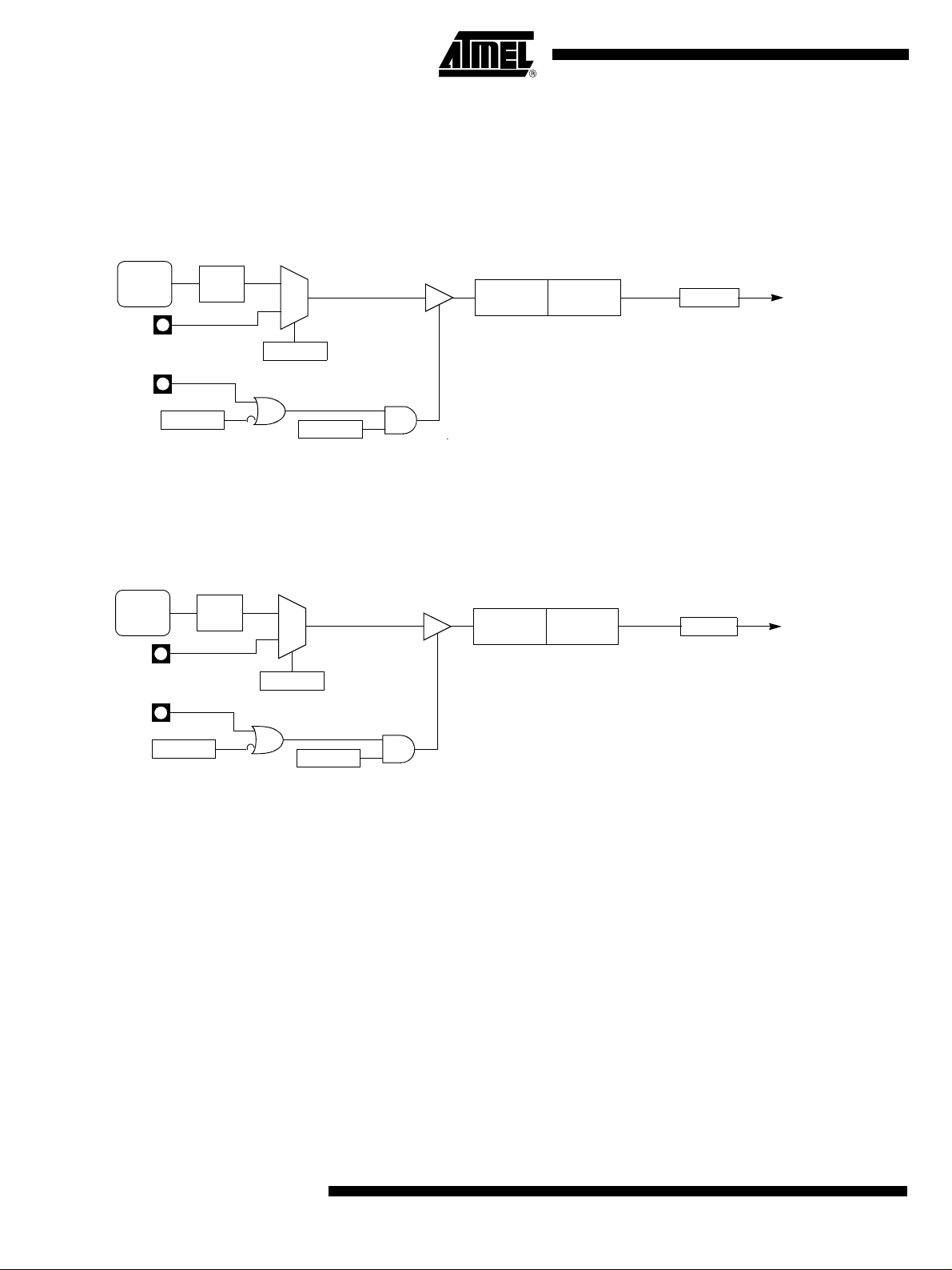
A/T89C51CC01
Mode 0 (13-bit Timer) Mode 0 configures Ti mer 0 as an 13-bit Tim er which is s et up as an 8-bit Ti mer (TH0
t
t
See the “Clock” section
register) with a modulo 32 prescaler implemented with the lower five bits of TL0 register
(see Figure 31). The upper three bits of TL0 register are indeterminate and should be
ignored. Prescaler overflow increments TH0 register.
Figure 31. Timer/Counter x (x = 0 or 1) in Mode 0
See the “Clock” section
FTx
CLOCK
÷ 6
0
1
THx
(8 bits)
TLx
(5 bits)
Overflow
TFx
TCON reg
Timer x
Interrup
Reques
Tx
C/Tx#
TMOD reg
INTx#
GATEx
TMOD reg
TRx
TCON reg
Mode 1 (16-bit Timer) Mode 1 configures Timer 0 as a 16-bit Timer with TH0 and TL0 registers connected in
cascade (see Figure 32). The selected input increments TL0 register.
Figure 32. Timer/Counter x (x = 0 or 1) in Mode 1
FTx
CLOCK
Tx
INTx#
÷ 6
0
1
C/Tx#
TMOD reg
THx
(8 bits)
TLx
(8 bits)
Overflow
TFx
TCON reg
Timer x
Interrupt
Request
62
GATEx
TMOD reg
TRx
TCON reg
4129L–CAN–08/05
Page 63

A/T89C51CC01
t
t
t
t
t
t
Mode 2 (8-bit Timer with AutoReload)
Mode 2 configures Timer 0 as an 8-b it Timer (TL0 register) tha t automatically reloads
from TH0 register (see Figure 33). TL0 overflow sets TF0 flag in TCON register and
reloads TL0 with the contents of TH0, which is preset by software. When the interrupt
request is servic ed, ha rdware clears TF0. The reload l eaves TH0 unch anged. The nex t
reload value may be changed at any time by writing it to TH0 register.
Figure 33. Timer/Counter x (x = 0 or 1) in Mode 2
See the “Clock” section
FTx
CLOCK
÷ 6
0
1
TLx
(8 bits)
Overflow
TFx
TCON reg
Timer x
Interrup
Reques
Tx
C/Tx#
TMOD reg
INTx#
GATEx
TMOD reg
TRx
TCON reg
THx
(8 bits)
Mode 3 (Two 8-bit Timers) Mode 3 configures Timer 0 such that registers T L0 and TH0 operate as separate 8-bit
Timers (see Figure 34). This mode is provided for applications requiring an additional 8bit Timer or Counter. TL0 uses the Timer 0 control bits C/T0# and GATE0 in TMOD register, and TR 0 and TF0 in TCON register in the normal manner. TH0 is locked into a
Timer function (counting F
/6) and takes over use of the Timer 1 in terrupt (TF1) and
PER
run control (TR1) bits. Thus , operation of Tim er 1 is restricted when Timer 0 is in mod e
3.
Figure 34. Timer/Counter 0 in Mode 3: Two 8-bit Counters
FTx
CLOCK
÷ 6
T0
INT0#
GATE0
TMOD.3
FTx
CLOCK
÷ 6
See the “Clock” section
0
1
C/T0#
TMOD.2
TR0
TCON.4
TR1
TCON.6
TL0
(8 bits)
TH0
(8 bits)
Overflow
Overflow
TF0
TCON.5
TF1
TCON.7
Timer 0
Interrup
Reques
Timer 1
Interrup
Reques
4129L–CAN–08/05
63
Page 64

A/T89C51CC01
Timer 1 Timer 1 is identical to Timer 0 excepted for Mode 3 which is a hold-count mode. The fol-
lowing comments help to understand the differences:
• Timer 1 functions as either a Timer or event Counter in three modes of operation.
Figure 31 to Figure 33 show the logical configuration for modes 0, 1, and 2. Timer
1’s mode 3 is a hold-count mode.
• Timer 1 is controlled by the four high-order bits of TMOD register (see Figure 41)
and bits 2, 3, 6 and 7 of TCON register (see Figure 40). TMOD register selects the
method of Timer gating (GATE1), Timer or Counter operation (C/T1#) and mode of
operation (M11 and M01). TCON register provides Timer 1 control functions:
overflow flag (TF1), run control bit (TR1), interrupt flag (IE1) and interrupt type
control bit (IT1).
• Timer 1 can serve as the Baud Rate Generator for the Serial Port. Mode 2 is best
suited for this purpose.
• For normal Timer operation (GATE1 = 0), setting TR1 allows TL1 to be incremented
by the selected input. Setting GATE1 and TR1 allows external pin INT1# to control
Timer operation.
• Timer 1 overflow (count rolls over from all 1s to all 0s) sets the TF1 flag generating
an interrupt request.
• When Timer 0 is in mode 3, it uses Timer 1’s overflow flag (TF1) and run control bit
(TR1). For this situation, use Timer 1 only for applications that do not require an
interrupt (such as a Baud Rate Generator for the Serial Port) and switch Timer 1 in
and out of mode 3 to turn it off and on.
• It is important to stop Timer/Counter before changing mode.
Mode 0 (13-bit Timer) Mode 0 configures Timer 1 as a 13-bit Timer, which is set up as an 8-bit Timer (TH1 reg-
ister) with a modulo-32 prescaler implemented with the lower 5 bits of the TL1 register
(see Figure 31) . The up per 3 bits of TL1 re gister are igno red. Pre scal er overf low inc rements TH1 register.
Mode 1 (16-bit Timer) Mode 1 configures Timer 1 as a 16-bit Timer with TH1 and TL1 registers connected in
cascade (see Figure 32). The selected input increments TL1 register.
Mode 2 (8-bit Timer with AutoReload)
Mode 3 (Halt) Placing Timer 1 in mode 3 causes it to halt and ho ld its coun t. This can be used to halt
Mode 2 configures Timer 1 as an 8-bit Timer (TL1 register) with automatic reload from
TH1 register on ove rflow ( see Figu re 33 ). TL1 o verflo w sets T F1 flag in TCO N regis ter
and reloads TL1 with the contents of TH1, which is preset by software. The reload
leaves TH1 unchanged.
Timer 1 when TR1 run control bit is not available i.e. when Timer 0 is in mode 3.
Interrupt Each Timer handles one interrupt source that is the timer overflow flag TF0 or TF1. This
flag is set every time an overfl ow oc c urs. Fla gs are cl eared when v ec toring to the Timer
interrupt routine. Interrupts are enabled by setting
interrupts are globally enabled by setting EA bit in IEN0 register.
ETx bit in IEN0 register. This assumes
64
4129L–CAN–08/05
Page 65

Figure 35. Timer Interrupt System
A/T89C51CC01
TF0
TCON.5
TF1
TCON.7
ET0
IEN0.1
ET1
IEN0.3
Timer 0
Interrupt Request
Timer 1
Interrupt Request
4129L–CAN–08/05
65
Page 66

A/T89C51CC01
Registers Table 40. TCON Register
TCON (S:88h)
Timer/Counter Control Register
76543210
TF1 TR1 TF0 TR0 IE1 IT1 IE0 IT0
Bit
Number
7TF1
6TR1
5TF0
4TR0
3IE1
2IT1
1IE0
Bit
Mnemonic Description
Timer 1 Overflow Flag
Cleared by hardware when processor vectors to interrupt routine.
Set by hardware on Timer/Counter overflow, when Timer 1 register overflows.
Timer 1 Run Control Bit
Clear to turn off Timer/Counter 1.
Set to turn on Timer/Counter 1.
Timer 0 Overflow Flag
Cleared by hardware when processor vectors to interrupt routine.
Set by hardware on Timer/Counter overflow, when Timer 0 register overflows.
Timer 0 Run Control Bit
Clear to turn off Timer/Counter 0.
Set to turn on Timer/Counter 0.
Interrupt 1 Edge Flag
Cleared by hardware when interrupt is processed if edge-triggered (see IT1).
Set by hardware when external interrupt is detected on INT1# pin.
Interrupt 1 Type Control Bit
Clear to select low level active (level triggered) for external interrupt 1 (INT1#).
Set to select falling edge active (edge triggered) for external interrupt 1.
Interrupt 0 Edge Flag
Cleared by hardware when interrupt is processed if edge-triggered (see IT0).
Set by hardware when external interrupt is detected on INT0# pin.
66
0IT0
Interrupt 0 Type Control Bit
Clear to select low level active (level triggered) for external interrupt 0 (INT0#).
Set to select falling edge active (edge triggered) for external interrupt 0.
Reset Value = 0000 0000b
4129L–CAN–08/05
Page 67

A/T89C51CC01
Table 41. TMOD Register
TMOD (S:89h)
Timer/Counter Mode Control Register
76543210
GATE1 C/T1# M11 M01 GATE0 C/T0# M10 M00
Bit
Number
7GATE1
6C/T1#
5M11Timer 1 Mode Select Bits
4M01
3GATE0
2C/T0#
1M10
0
Bit
Mnemonic Description
Timer 1 Gating Control Bit
Clear to enable Timer 1 whenever TR1 bit is set.
Set to enable Timer 1 only while INT1# pin is high and TR1 bit is set.
Timer 1 Counter/Timer Select Bit
Clear for Timer operation: Timer 1 counts the divided-down system clock.
Set for Counter operation: Timer 1 counts negative transitions on external pin T1.
M01 Operating mode
M11
0 0 Mode 0: 8-bit Timer/Counter (TH1) with 5-bit prescaler (TL1).
0 1 Mode 1: 16-bit Timer/Counter.
1 0 Mode 2: 8-bit auto-reload Timer/Counter (TL1)
1 1 Mode 3: Timer 1 halted. Retains count
Timer 0 Gating Control Bit
Clear to enable Timer 0 whenever TR0 bit is set.
Set to enable Timer/Counter 0 only while INT0# pin is high and TR0 bit is set.
Timer 0 Counter/Timer Select Bit
Clear for Timer operation: Timer 0 counts the divided-down system clock.
Set for Counter operation: Timer 0 counts negative transitions on external pin T0.
Timer 0 Mode Select Bit
M10
M00 Operating mode
0 0 Mode 0: 8-bit Timer/Counter (TH0) with 5-bit prescaler (TL0).
0 1 Mode 1: 16-bit Timer/Counter.
M00
1 0 Mode 2: 8-bit auto-reload Timer/Counter (TL0)
1 1 Mode 3: TL0 is an 8-bit Timer/Counter
TH0 is an 8-bit Timer using Tim e r 1’s TR0 and TF0 bits.
Notes: 1. Reloaded from TH1 at overflow.
2. Reloaded from TH0 at overflow.
(1)
(2)
4129L–CAN–08/05
Reset Value = 0000 0000b
67
Page 68

A/T89C51CC01
Table 42. TH0 Register
TH0 (S:8Ch)
Timer 0 High Byte Register
76543210
––––––––
Bit
Number
7:0 High Byte of Timer 0.
Bit
Mnemonic Description
Reset Value = 0000 0000b
Table 43. TL0 Register
TL0 (S:8Ah)
Timer 0 Low Byte Register
76543210
––––––––
Bit
Number
7:0 Low Byte of Timer 0.
Bit
Mnemonic Description
Reset Value = 0000 0000b
Table 44. TH1 Register
TH1 (S:8Dh)
Timer 1 High Byte Register
68
76543210
––––––––
Bit
Number
7:0 High Byte of Timer 1.
Bit
Mnemonic Description
Reset Value = 0000 0000b
4129L–CAN–08/05
Page 69

A/T89C51CC01
Table 45. TL1 Register
TL1 (S:8Bh)
Timer 1 Low Byte Register
76543210
––––––––
Bit
Number
7:0 Low Byte of Timer 1.
Bit
Mnemonic Description
Reset Value = 0000 0000b
4129L–CAN–08/05
69
Page 70

A/T89C51CC01
Timer 2 The T89C51CC01 timer 2 is compatible with timer 2 in the 80C52.
see section “Clock”
It is a 16-bit timer/counter: the count is maintained by two eight-bit timer registers, TH2
and TL2 that are cascade- connected. It is controlled by T2CON register (See Table )
and T2MOD register (See Table 48). Timer 2 operation is similar to Timer 0 and Timer
1. C/T2
timer clock. Setting TR2 allows TL2 to be incremented by the selected input.
Timer 2 includes the following enhancements:
• Auto-reload mode (up or down counter)
• Programmable clock-output
Auto-Reload Mode The auto-reload mode configures timer 2 as a 16-bit timer or event counter with auto-
matic reload. This feature is controlled by the DCEN bit in T2MOD register (See
Table 48). Setting the DCEN bit enables timer 2 to count up or down as shown in
Figure 36. In this mode the T2EX pin controls the counting direction.
When T2EX is high, timer 2 counts up. Timer overflow occurs at FFFFh which sets the
TF2 flag and gene rates an inter rupt requ est. The overfl ow a lso cause s th e 16 -bit v alu e
in RCAP2H and RCAP2L registers to be loaded into the timer registers TH2 and TL2.
When T2EX is low, tim er 2 count s do wn. Timer un derfl ow occur s when the c ount in th e
timer registers TH2 and TL2 equals the value stored in RCAP2H and RCAP2L registers.
The underflow sets TF2 flag and reloads FFFFh into the timer registers.
The EXF2 bit toggles wh en t ime r 2 ov erflo w or un der flow, d epending on the direction of
the count. EXF2 does not generate an interrupt. This bit can be used to provide 17-bit
resolution.
selects F
/6 (timer operation) or external pin T2 (counter operation) as
T2 clock
Figure 36. Auto-Reload Mode Up/Down Counter
FT2
CLOCK
T2
:6
0
1
CT/2
T2CON.1
(DOWN COUNTING RELOAD VALUE)
FFh
(8-bit)
TL2
(
8-bit)
RCAP2L
(8-bit)
(UP COUNTING RELOAD VALUE)
FFh
(8-bit)
TH2
(8-bit)
RCAP2H
(8-bit)
TR2
T2CON.2
T2EX:
1=UP
2=DOWN
TOGGLE
TF2
T2CONreg
T2CONreg
EXF2
TIMER 2
INTERRUPT
70
4129L–CAN–08/05
Page 71

A/T89C51CC01
Programmable ClockOutput
In clock-out mode, timer 2 operates as a 50%-duty-cycle, programmable clock generator (See Figure 37). The input clock increments TL2 at frequency F
/2. The timer
OSC
repeatedly counts to overflow from a loaded value. At overflow, the contents of RCAP2H
and RCAP2L regi ster s ar e lo ade d into TH 2 a nd T L2. In th is m ode , t ime r 2 ov er fl ows d o
not generate interrupts. The formula gives the clock-out frequency depending on the
system oscillator frequenc y and the val ue in the RCAP2H and RCAP2L registers:
Clock OutFrequen cy–
For a 16 MHz system clock in x1 mode, timer 2 has a programmable frequency range of
61 Hz (F
OSC
16)
/2
to 4 MHz (F
---------------------------------------------------------------------------------------- -
=
4 65536 RC AP2H– RCAP2L⁄()×
/4). The generated clock signal is b r ough t out t o T 2 pi n
OSC
FT2clock
(P1.0).
Timer 2 is programmed for the clock-out mode as follows:
• Set T2OE bit in T2MOD register.
•Clear C/T2
bit in T2CON register.
• Determine the 16-bit reload value from the formula and enter it in RCAP2H/RCAP2L
registers.
• Enter a 16-bit initial value in timer registers TH2/TL2. It can be the same as the
reload value or different depending on the application.
• To start the timer, set TR2 run control bit in T2CON register.
Figure 37. Clock-Out Mode
CLOCK
T2
T2EX
FT2
It is possible to use timer 2 as a baud rate generator and a c lock generator simultaneously. For this configuration, the baud rates and clock frequencies are not
independent since both functions use the values in the RCAP2H and RCAP2L registers.
TH2
(8-bit)
RCAP2H
(8-bit)
T2OE
T2MOD reg
OVERFLOW
TIMER 2
INTERRUPT
Toggle
Q
Q D
TR2
T2CON.2
EXEN2
T2CON reg
TL2
(8-bit)
RCAP2L
(8-bit)
EXF2
T2CON reg
4129L–CAN–08/05
71
Page 72

A/T89C51CC01
Registers Table 46. T2CON Register
T2CON (S:C8h)
Timer 2 Control Register
76543210
TF2 EXF2 RCLK TCLK EXEN2 TR2 C/T2# CP/RL2#
Bit
Number
7TF2
6EXF2
5 RCLK
4TCLK
3EXEN2
2TR2
Bit
Mnemonic Description
Timer 2 Overflow Flag
TF2 is not set if RCLK=1 or TCLK = 1.
Must be cleared by software.
Set by hardware on timer 2 overflow.
Timer 2 External Flag
Set when a capture or a reload is caused by a negative transition on T2EX pin if
EXEN2=1.
Set to cause the CPU to vector to timer 2 interrupt routine when timer 2 interrupt
is enabled.
Must be cleared by software.
Receive Clock bit
Clear to use timer 1 overflow as receive clock for serial port in mode 1 or 3.
Set to use timer 2 overflow as receive clock for serial port in mode 1 or 3.
Transmit Clock bit
Clear to use timer 1 overflow as transmit clock for serial port in mode 1 or 3.
Set to use timer 2 overflow as transmit clock for serial port in mode 1 or 3.
Timer 2 External Enable bit
Clear to ignore events on T2EX pin for timer 2 operation.
Set to cause a capture or reload when a negative transition on T2EX pin is
detected, if timer 2 is not used to clock the serial port.
Timer 2 Run Control bit
Clear to tur n off timer 2.
Set to turn on ti mer 2.
72
1C/T2#
0 CP/RL2#
Timer/Counter 2 Select bit
Clear for timer operation (input from internal clock system: F
Set for counter operation (input from T2 input pin).
Timer 2 Captur e /Reload bit
If RCLK=1 or TCLK=1, CP/RL2# is ignored and timer is forced to auto-reload on
timer 2 overflow.
Clear to auto-reload on timer 2 overflows or negative transitions on T2EX pin if
EXEN2=1.
Set to capture on negative transitions on T2EX pin if EXEN2=1.
Reset Value = 0000 0000b
Bit addressable
).
OSC
4129L–CAN–08/05
Page 73

A/T89C51CC01
Table 47. T2MOD Register
T2MOD (S:C9h)
Timer 2 Mode Control Register
76543210
------T2OEDCEN
Bit
Number
7-
6-
5-
4-
3-
2-
1T2OE
0 DCEN
Bit
Mnemonic Description
Reserved
The value read from this bit is indeterminate. Do not set this bit.
Reserved
The value read from this bit is indeterminate. Do not set this bit.
Reserved
The value read from this bit is indeterminate. Do not set this bit.
Reserved
The value read from this bit is indeterminate. Do not set this bit.
Reserved
The value read from this bit is indeterminate. Do not set this bit.
Reserved
The value read from this bit is indeterminate. Do not set this bit.
Timer 2 Output Enable bit
Clear to program P1.0/T2 as clock input or I/O port.
Set to program P1.0/T2 as clock output.
Down Counter Enable bit
Clear to disable timer 2 as up/down counter.
Set to enable timer 2 as up/down counter.
Reset Value = XXXX XX00b
Not bit addressable
4129L–CAN–08/05
Table 48. TH2 Register
TH2 (S:CDh)
Timer 2 High Byte Register
76543210
--------
Bit
Number
7-0 High Byte of Timer 2.
Bit
Mnemonic Description
Reset Value = 0000 0000b
Not bit addressable
73
Page 74

A/T89C51CC01
Table 49. TL2 Register
TL2 (S:CCh)
Timer 2 Low Byte Register
76543210
--------
Bit
Number
7-0 Low Byte of Timer 2.
Bit
Mnemonic Description
Reset Value = 0000 0000b
Not bit addressable
Table 50. RCAP2H Register
RCAP2H (S:CBh)
Timer 2 Reload/Capture High Byte Register
76543210
--------
Bit
Number
7-0 High Byte of Timer 2 Reload/Capture.
Bit
Mnemonic Description
Reset Value = 0000 0000b
Not bit addressable
Table 51. RCAP2L Register
74
RCAP2L (S:CA
T
IMER 2 REload/Capture Low Byte Register
76543210
--------
Bit
Number
7-0 Low Byte of Timer 2 Reload/Ca pture.
H)
Bit
Mnemonic Description
Reset Value = 0000 0000b
Not bit addressable
4129L–CAN–08/05
Page 75

A/T89C51CC01
Watchdog Timer T89C51CC01 contains a powerful programmable hardware Watchdog Timer (WDT) that
automatically resets the chip if it software fails to reset the WDT before the selected time
interval has elapsed. It permits large Time-Out ranking from 16ms to 2s @Fosc =
12MHz in X1 mode.
This WDT consists of a 14-bit counter plus a 7-bit programmable counter, a Watchdog
Timer reset regist er (WDTRS T ) a nd a Wa tch dog T imer pr ogram min g (WD T PRG) r egister. When exiting reset, the WDT is -by default- disable.
To enable the WDT, the user has to wr ite the sequenc e 1EH and E1H into WDTR ST
register no instruction in between. When the Watchdog Timer is enabled, it will increment every machine cycle while the oscillator is running and there is no way to disable
the WDT except through reset (either hardware reset or WDT overflow reset). When
WDT overflows, it will generate an output RESET pulse at the RST pin. The RESET
pulse duratio n is 96xT
should be serviced in those sections of code that will periodically be executed within the
time required to prevent a WDT reset
Note: When the Watchdog is enable it is impossible to change its period.
Figure 38. Watchdog Timer
, where T
OSC
OSC
=1/F
. To make the best use of the WDT, it
OSC
Fwd Clock
RESET
WDTPRG
Fwd
CLOCK
WDTRST
Enable
14-bit COUNTER
÷ PS
WR
÷ 6
Decoder
Control
CPU and Peripheral
Clock
7-bit COUNTER
Outputs
4129L–CAN–08/05
-
-
-
-
-
2
0
1
RESET
75
Page 76

A/T89C51CC01
Watchdog Programming The three lower bits (S0, S1, S2) located into WDTPRG register permit to program the
WDT duration.
Table 52. Machine Cycle Count
S2 S1 S0 Machine Cycle Count
000 2
001 2
010 2
011 2
100 2
101 2
110 2
111 2
To compute WD Time-Out, the following formula is applied:
F
FTime Out
-----------------------------------------------------------------
=–
12 2
wd
142Svalue
×()1–()×
14
- 1
15
- 1
16
- 1
17
- 1
18
- 1
19
- 1
20
- 1
21
- 1
Note: Svalue represents the decimal value of (S2 S1 S0)
The following table outlines the time-out val ue for Fosc
= 12 MHz in X1 mode
XTAL
Table 53. Time-Out Computation
S2 S1 S0 Fosc = 12 MHz Fosc = 16 MHz Fosc = 20 MHz
0 0 0 16.38 ms 12.28 ms 9.82 ms
0 0 1 32.77 ms 24.57 ms 19.66 ms
0 1 0 65.54 ms 49.14 ms 39.32 ms
0 1 1 131.07 ms 98.28 ms 78.64 ms
1 0 0 262.14 ms 196.56 ms 157.28 ms
1 0 1 524.29 ms 393.12 ms 314.56 ms
1 1 0 1.05 s 786.24 ms 629.12 ms
1 1 1 2.10 s 1.57 s 1.25 s
76
4129L–CAN–08/05
Page 77

A/T89C51CC01
Watchdog Timer During Power-down Mode and Idle
In Power-down mode the oscill ator stops, whi ch means the W DT also stops . While in
Power-down mode, the user does not need to service the WDT. There are 2 methods of
exiting Power-down mode: by a hardware reset or via a level activated external interrupt
which is enabl ed p rio r to e nter ing Po wer-do wn mode . Wh en Powe r-down is exite d wit h
hardware reset, the Watchdog is disabled. Exiting Power-down with an interrupt is significantly different. The interrupt shall be held low long enough for the oscillator to
stabilize. Wh en t he inter rupt is br ought h igh, the in terrupt is se rvice d. To p reven t the
WDT from resetting the device while the interrupt pin is held low, the WDT is not started
until the interrup t is pulled high. It is suggested that the WDT be reset during the interrupt service for the interrupt used to exit Power-down.
To ensure that the WDT does not overflow within a few states of exiting powerdown, it is
best to reset the WDT just before entering powerdown.
In the Idle mode, the oscillator continues to run. To prevent the WDT from resetting
T89C51CC01 while in Idle mode, the user should always set up a timer that will periodically exit Idle, service the WDT, and re-enter Idle mode.
Register Table 54. WDTPRG Register
WDTPRG (S:A7h)
Watchdog Timer Duration Programming Register
76543210
–––––S2S1S0
Bit
Number
7-
6-
5-
4-
3-
2S2
1S1
0S0
Bit
Mnemonic Description
Reserved
The value read from this bit is indeterminate. Do not set this bit.
Reserved
The value read from this bit is indeterminate. Do not set this bit.
Reserved
The value read from this bit is indeterminate. Do not set this bit.
Reserved
The value read from this bit is indeterminate. Do not set this bit.
Reserved
The value read from this bit is indeterminate. Do not set this bit.
Watchdog Timer Duration selection bit 2
Work in conjunction with bit 1 and bit 0.
Watchdog Timer Duration selection bit 1
Work in conjunction with bit 2 and bit 0.
Watchdog Timer Duration selection bit 0
Work in conjunction with bit 1 and bit 2.
Reset Value = XXXX X000b
4129L–CAN–08/05
77
Page 78

A/T89C51CC01
Table 55. WDTRST Register
WDTRST (S:A6h Write only)
Watchdog Timer Enable Register
76543210
––––––––
Bit
Number
7 - Watchdog Control Value
Bit
Mnemonic Description
Reset Value = 1111 1111b
Note: The WDRST register is used to reset/enable the WDT by writing 1EH then E1H in
sequence without instruction between these two sequences.
78
4129L–CAN–08/05
Page 79

A/T89C51CC01
CAN Controller The CAN Controller provides al l th e fe atu re s re qui red to implement the serial c om mun i-
cation protocol CAN as defined by BOSCH GmbH. The CAN specification as referred to
by ISO/11898 (2.0A and 2.0B) for high speed and ISO/11519-2 for low speed. The CAN
Controller is able to handle al l typ es of fram es (D ata, Remo te, Erro r and Ov erlo ad) and
achieves a bitrate of 1-Mbit/sec. at 8 MHz
Note: 1. At BRP = 1 sampling point will be fixed.
CAN Protocol The CAN proto col is a n interna tional s tand ard define d in the I SO 11898 for high sp eed
and ISO 11519-2 for low speed.
Principles CAN is based on a broadcast communication mechanism. This broadcast communica-
tion is achieved by using a message oriented transmission protocol. These messages
are identified by using a message identifier. Such a message identifier has to be unique
within the whole network and it defines not only the content but also the priority of the
message.
The priority at which a message is transmitted compared to another less urgent message is spe cifie d by the i dent ifier of eac h message. The priorities are laid down during
system design in the form of corresponding binary values and cannot be changed
dynamically. The identifier with the lowest binary number has the highest priority.
Bus access confl icts are r esolved by bit-wis e arbitrati on on the i dentifiers involved by
each node observing the bus level bit for bit. This happens in accordance with the "wired
and" mechanism, b y w hic h t he d omi nan t state overwrites the rece ss i ve sta te. T h e c ompetition for bus all ocation is lost by a ll n odes with r ecessi ve tr ansm ission and domi nant
observation. All the "los ers" a utomati cally become recei vers of the messag e with the
highest priority and do not re-attempt transmission until the bus is available again.
1
Crystal frequency in X2 mode.
Message Formats The CAN proto col supports two me ssage frame formats, the only essential difference
being in the length of the identifier. The CAN standard frame, also known as CAN 2.0 A,
supports a length of 11 b its for the identi fier , and the C AN exte nded frame , als o know n
as CAN 2.0 B, supports a length of 29 bits for the identifier.
Can Standard Frame
Figure 39. CAN Standard Fra mes
Data Frame
Bus Idle Bus Idle
Interframe
Space
SOF
SOF
11-bit identifier
ID10..0
Arbitration
Field
RTR
4-bit DLC
IDE r0 ACK
DLC4..0
Control
Field
0 - 8 bytes
Data
Field
15-bit CRC
CRC
Field
CRC
del.
ACK
Field
ACK
del.
7 bits
End of
Frame
Intermission
3 bits
Interframe
(Indefinite)
Space
Remote Frame
Bus Idle Bus Idle
Interframe
Space
SOF
SOF
11-bit identifier
ID10..0
Arbitration
Field
RTR
A message in the CAN standard frame format begins with the "Start Of Frame (SOF)",
this is followed by the "Arbitration field" which consist of the identifier and the "Remote
Transmission Request (RTR)" bit used to distinguish between the data frame and the
data request frame called remote frame. The following "Control field" contains the "IDentifier Extension (IDE)" bit and the "Da ta Length Code (DLC)" used to indicate the
4-bit DLC
IDE r0 ACK
DLC4..0
Control
Field
15-bit CRC
CRC
Field
CRC
del.
ACK
Field
ACK
del.
7 bits
End of
Frame
Intermission
3 bits
Interframe
(Indefinite)
Space
4129L–CAN–08/05
79
Page 80

A/T89C51CC01
number of followin g data byte s in the "D ata field". In a remote frame, the DLC contains
)
the number of request ed data bytes . The "Data field" that foll ows can hol d up to 8 data
bytes. The fra me integri ty is gua ranteed by the fol lowing "Cy clic Redund ant Check
(CRC)" sum . The "A CKnow ledge ( ACK) field" comp romise s the A CK slot and th e ACK
delimiter. The bit in t he A C K slot i s se nt as a re ce ss iv e bit and is ov erwr itt en a s a dom inant bit by the receivers which have at this time received the data correctly. Correct
messages are acknowledged by the receivers regardless of the result of the acceptance
test. The end of the messa ge is in dicat ed by "End Of Fram e (EOF) ". The "In termi ssion
Frame Space (IFS)" is the minimum number of bits separating consecutive messages. If
there is no following bus access by any node, the bus remains idle.
CAN Extended Frame
Figure 40. CAN Extended Frames
Data Frame
Bus Idle Bus Idle
11-bit base identifier
SOF
SOF
IDT28..18
SRR
18-bit identifier extension
IDE ACK
ID17..0
RTR
r0r1
4-bit DLC
DLC4..0
0 - 8 bytes
15-bit CRC
CRC
del.
ACK
del.
7 bits
Intermission
3 bits
(Indefinite
Interframe
Space
Arbitration
Field
Control
Field
Data
Field
CRC
Field
ACK
Field
End of
Frame
Interframe
Space
Remote Frame
Bus Idle Bus Idle
Interframe
Space
11-bit base identifier
SOF
SOF
IDT28..18
SRR
Format Co-existence As the two form ats have to co-exist on one bus, it is lai d down which message has
18-bit identifier extension
IDE r0
Arbitration
Field
ID17..0
RTR
4-bit DLC
r1 ACK
DLC4..0
Control
Field
15-bit CRC
CRC
Field
CRC
del.
ACK
ACK
Field
del.
7 bits
End of
Frame
Intermission
3 bits
Interframe
(Indefinite)
Space
A message in th e CAN extended frame form at is li kely the same as a message in CA N
standard frame format. The difference is the length of the identifier used. The identifier is
made up of the existing 11-bit identi fier (base id entifier) and an 18-bit extens ion (identifier extension). The d istin ction between CAN stan dard fra me forma t an d CAN e xte nde d
frame format is made by using the IDE bit which is trans mi tted as d omi nan t in cas e o f a
frame in CAN standard frame format, and transmitted as recessive in the other case.
higher priority on the bus in the case of bus access collision with different formats and
the same identifier / base identifier: The message in CAN standard frame format always
has priority over the message in extended format.
There are three different types of CAN modules available:
– 2.0A - Considers 29 bit ID as an error
– 2.0B Passive - Ignores 29 bit ID messages
– 2.0B Active - Handles both 11 and 29 bit ID Messages
Bit Timing To ensure co rrect sampling up to the la st bit, a CAN node needs to re-sync hronize
throughout the entire frame. This is done at the beginning of each message with the falling edge SOF and on each recessive to dominant edge.
Bit Construction One CAN bit time is specified as four non-overlapping time segm ents. Ea ch segment is
constructed from an in teger multiple of the T ime Quan tum. T he Ti me Q u antu m or TQ is
the smallest discrete timing resolution used by a CAN node.
80
4129L–CAN–08/05
Page 81

A/T89C51CC01
Figure 41. CAN Bit Construction
CAN Frame
(producer)
Transmission Point
(producer)
Nominal CAN Bit Time
Time Quantum
(producer)
Segments
(producer)
Segments
(consumer)
SYNC_SEG
propagation
delay
Synchronization Segment The first segment is used to synchronize the various bus nodes.
On transmission, at the start of thi s segment, the curren t bit level is output. If th ere is a
bit state change betwe en th e prev io us bit and t he c ur rent b it, th en t he bu s s tat e ch ange
is expected to occur within this segment by the receiving nodes.
PROP_SEG PHASE_SEG_1 PHASE_SEG_2
SYNC_SEG
PROP_SEG PHASE_SEG_1 PHASE_SEG_2
Sample Point
Propagation Time Segment This segment is used to compensate for signal delays across the network.
This is neces sary to c ompensate for signa l propag ation d elays on the bus l ine and
through the transceivers of the bus nodes.
Phase Segment 1 Phase Segment 1 is used to compensate for edge phase errors.
This segment may be lengthened during resynchronization.
Sample Point The sample point is the point of time at which the bus level is read and interpreted as the
value of the respective bit. Its location is at the end of Phase Segment 1 (between the
two Phase Segments).
Phase Segment 2 This segment is also used to compensate for edge phase errors.
This segment may be shortened during resynchronization, but the length has to be at
least as long as the information processing time and may not be more than the length of
Phase Segment 1.
Information Processing Time It is the time required for the logic to determine the bit level of a sampled bit.
The Information pr ocessin g Time begin s at the sam ple point, is measured i n TQ and is
fixed at 2 TQ for the Atmel CAN. Since Phase Segment 2 also begins at the sample
point and is t he las t segm ent in the bi t time, Phase Segme nt 2 m inimum shall not be
less than the Information processing Time.
Bit Lengthening As a result of resynchronization, Phase Segment 1 may be lengthened or Phase Seg-
ment 2 may be shortened to compensa te for osc illator tolerances. If, for ex ample, the
transmitter oscillator is slower tha n the re ceiver oscillator , the nex t falling e dge use d for
resynchronization may be delayed. So Phase Segment 1 is lengthened in order to
adjust the sample point and the end of the bit time.
4129L–CAN–08/05
81
Page 82
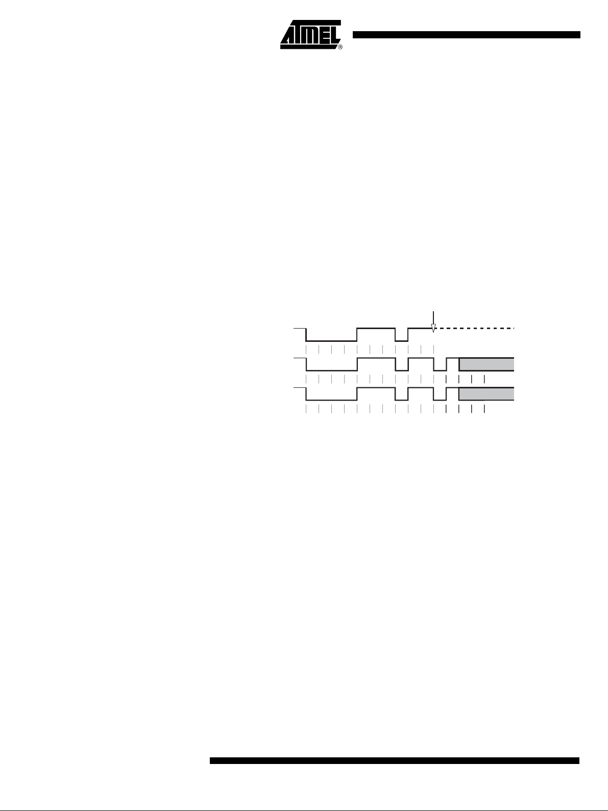
A/T89C51CC01
Bit Shortening If, on the other hand, the transmitter oscillator is faster than the receiver one, the next
-
falling edge use d for resync hroni zation ma y be too earl y. So Phas e Segment 2 in bit N
is shortened in order to adjust the sample point for bit N+1 and the end of the bit time
Synchronization Jump Width The limit to the amount of lengthening or shortening of the Phase Segments is set by the
Resynchronization Jump Width.
This segment may not be longer than Phase Segment 2.
Programming the Sample Point Programming of the sample point allows "tuning" of the characteristics to suit the bus.
Early sampling allo ws more Tim e Quanta in the Phase Se gment 2 so the Synchron ization Jump Width can be programmed to its maximum. This maximum capacity to
shorten or lengthen the bit time decreases the sensitivity to node oscillator tolerances,
so that lower cost oscillators such as ceramic resonators may be used.
Late sampling allows more Time Quanta in the Propagation Time Segment which allows
a poorer bus topology and maximum bus length.
Arbitration Fig ure 42. Bus Arbitration
Arbitration lost
node A
TXCAN
node B
TXCAN
CAN bus
ID10 ID9 ID8 ID7 ID6 ID5 ID4 ID3 ID2 ID1 ID0
SOF
SOF
Node A loses the bus
Node B wins the bus
RTR IDE
- - - - - - - -
The CAN protocol handles bus accesses according to the concept called “Carrier Sense
Multiple Access with Arbitration on Message Priority”.
During transmission, arbitra tion on the CAN bus can be lost to a com peting device with
a higher priority CAN Identifier. This arbitration concept avoids collisions of messages
whose transmission was started by more than one node simultaneously and makes sure
the most important message is sent first without time loss.
The bus access conflic t is res olved du ring the a rbitra tion fi eld mostl y over the iden tifier
value. If a data frame and a remote frame wi th the same ident ifier are initi ated at the
same time, the data frame prevails over the remote frame (c.f. RTR bit).
Errors The CAN protocol signals any errors immediately as they occur. Three error detection
mechanisms are implemented at the message level and two at the bit level:
Error at Message Level • Cyclic Redundancy Check (CRC)
The CRC safeguards the information in the frame by adding redundant check bits at
the transmission end. At the receiver these bits are re-computed and tested against
the received bits. If they do not agree there has been a CRC error.
82
•Frame Check
This mechanism verifies the structure of the transmitted frame by checking the bit
fields against the fixed format and the frame size. Errors detected by frame checks
are designated "format errors".
4129L–CAN–08/05
Page 83

A/T89C51CC01
•ACK Errors
As already mentioned frames received are acknowledged by all receivers through
positive acknowledgement. If no acknowledgement is received by the transmitter of
the message an ACK error is indicated.
Error at Bit Level • Monitoring
The ability of the transmitter to detect errors is based on the monitoring of bus
signals. Each node which transmits also observes the bus level and thus detects
differences between the bit sent and the bit received. This permits reliable detection
of global errors and errors local to the transmitter.
• Bit Stuffing
The coding of the individual bits is tested at bit level. The bit representation used by
CAN is "Non Return to Zero (NRZ)" coding, which guarantees maximum efficiency
in bit coding. The synchronization edges are generated by means of bit stuffing.
Error Signalling If one or more errors are discovered by at least one node using the above mechanisms,
the current transmission is aborted by sending an "error flag". This prevents other nodes
accepting the messa ge and thus ensures the cons istency of data thro ughout the network. After transmission of an erroneou s message that has been aborted, the sender
automatically re-attempts transmission.
CAN Controller Description
The CAN Controller accesses are made through SFR.
Several operations are possible by SFR:
• arithmetic and logic operations, transfers and program control (SFR is accessible by
direct addressing).
• 15 independent message objects are implemented, a pagination system manages
their accesses.
Any message o bj ec t c an be programmed in a r ec ept ion b u ffe r bl oc k ( ev en non -con secutive buffers ). For the r eceptio n of def ined mes sages on e or seve ral rec eiver me ssage
objects can be masked without participating in the buffer feature. An IT is generated
when the buffer is full. The frames foll owing the buffer-full interrupt will not be take n in to
account until at least one of the buffer message objects is re-enabled in reception.
Higher priority of a message object for reception or transmiss ion is given to the lower
message object number.
The programmable 16-b it Time r (CANT IMER ) is used to st amp e ach r eceive d and sent
message in the CANSTMP register. This timer starts counting as soon as the CAN controller is enabled by the ENA bit in the CANGCON register.
The Time Trigger Communication (TTC) protocol is supported by the T89C51CC01.
4129L–CAN–08/05
83
Page 84

A/T89C51CC01
Figure 43. CAN Controller Block Diagram
TxDC
RxDC
Bit
Timing
Logic
Error
Counter
Rec/Tec
Bit
Stuffing /Destuffing
Cyclic
Redundancy Check
Receive Transmit
CAN Controller Mailbox and Registers Organization
Page
Register
The paginat ion al lows m anage ment of the 3 21 re gister s inc luding 300( 15x20) Bytes of
mailbox via 34 SFR’s.
All actions on the message object window SFRs apply to the corresponding message
object registers pointed by the message object number find in the Page message object
register (CANPAGE) as illustrate in Figure 44.
DPR(Mailbox + Registers)
µC-Core Interface
Interface
Bus
Core
Control
Priority
Encoder
84
4129L–CAN–08/05
Page 85

Figure 44. CAN Controller Memory Organization
SFR’s On-chip CAN Controller registers
General Control
General Status
General Interrupt
Bit Timing - 1
Bit Timing - 2
Bit Timing - 3
Enable message object - 1
Enable message object - 2
Enable Interrupt
Enable Interrupt message object - 1
Enable Interrupt message object - 2
Status Interrupt message object - 1
Status Interrupt message object - 2
Timer Control
CANTimer High
CANTimer Low
TimTTC High
TimTTC Low
TEC counter
REC counter
Page message object
(message object number)(Data offset)
message object 0 - Status
message object Status
message object Control and DLC
Message Data
ID Tag - 1
ID Tag - 2
ID Tag - 3
ID Tag - 4
ID Mask - 1
ID Mask - 2
ID Mask - 3
ID Mask - 4
TimStmp High
TimStmp Low
message object 0 - Control and DLC
Ch.0 - Message Data - byte 0
8 Bytes
Ch.0 - ID Tag - 1
Ch.0 - ID Tag - 2
Ch.0 - ID Tag - 3
Ch.0 - ID Tag - 4
Ch.0 - ID Mask- 1
Ch.0 - ID Mask- 2
Ch.0 - ID Mask- 3
Ch.0 - ID Mask - 4
Ch.0 TimStmp High
Ch.0 TimStmp Low
15 message objects
A/T89C51CC01
message object 14 - Status
message object 14 - Control and DLC
Ch.14 - Message Data - byte 0
Ch.14 - ID Tag - 1
Ch.14 - ID Tag - 2
Ch.14 - ID Tag - 3
Ch.14 - ID Tag - 4
Ch.14 - ID Mask - 1
Ch.14 - ID Mask - 2
Ch.14 - ID Mask - 3
Ch.14 - ID Mask - 4
Ch.14 TimStmp High
Ch.14 TimStmp Low
4129L–CAN–08/05
message object Window SFRs
85
Page 86

A/T89C51CC01
Working on Message Objects The Page message object register (CANPAGE) is used to select one of the 15 message
objects. Then, message object Control (CANCONCH) and message object Status
(CANSTCH) are available for this selected message object number in the corresponding
SFRs. A single register (CANMSG) is used for the message. The mailbox pointer is
managed by the Page message object register with an auto-incrementation at the end of
each access. The range of this counter is 8.
Note that the maibox is a pure RAM, ded ic ate d to one mes sa ge ob je ct, wi tho ut over la p.
In most cases, i t is n ot neces sary to transfe r the rec eived me ssage i nto t he stand ard
memory. The message to be transmitted can be built directly in the maibox. Most calculations or tests can be executed in the mailbox area which provide quicker access.
CAN Controller Management
In order to enable the CAN Controller correctly the following registers have to be
initialized:
• General Control (CANGCON),
• Bit Timing (CANBT 1, 2 and 3),
• And for each page of 15 message objects
– m es sage obj ect Control (CANCONCH),
– message object Status (CANSTCH).
During operatio n, the CAN Ena ble mes sage obje ct regis ters 1 and 2 (C ANEN 1 an d 2)
gives a fast overview of the message objects availability.
The CAN messages can be handled by interrupt or polling modes.
A message object can be configured as follows:
• Transmit message object,
• Receive message object,
• Receive buffer message object.
• Disable
This configuration is made in the CONCH field of the CANCONCH register (see
Table 56).
When a message object is configured, the corresponding ENCH bit of CANEN 1 and 2
register is set.
86
Table 56. Configuration for CONCH1:2
CONCH 1 CONCH 2 Type of Message Object
0 0 disable
0 1 Transmitter
1 0 Receiver
1 1 Receiver buffer
When a Tran smitter or Recei ver act ion of a mes sage o bject is complet ed, the c orresponding ENCH bit of the CANEN 1 an d 2 regist er is clea red. In o rder to re -enable th e
message object, it is necessary to re-write the configuration in CANCONCH register.
Non-consecutive message objects can be used for all three types of message objects
(Transmitter, Receiver and Receiver buffer),
4129L–CAN–08/05
Page 87

A/T89C51CC01
Buffer Mode Any messag e obje ct can be u sed to de fine on e buffer , includ ing non -con secutiv e mes-
sage objects, and with no limitation in number of message objects used up to 15.
Each message object of the buffer must be initialized CONCH2 = 1 and CONCH1 = 1;
Figure 45. Buffer mode
message object 14
message object 13
message object 12
message object 11
message object 10
message object 9
message object 8
message object 7
message object 6
message object 5
message object 4
message object 3
message object 2
message object 1
message object 0
Block buffer
buffer 7
buffer 6
buffer 5
buffer 4
buffer 3
buffer 2
buffer 1
buffer 0
The same acceptance filter must be defined for each message objects of the buffer.
When there is no mask on the identifier or the IDE, all messages are accepted.
A received frame will always be stored in the lowest free message object.
When the flag Rxok is set o n one of the buffe r message objects, this m essage object
can then be read by t he a ppl ic ation. This flag must then be cl ear ed by th e software and
the message object re-enabled in buffer reception in order to free the message object.
The OVRBUF flag in the CANGIT register is set when the buffer is full. This flag can
generate an interrupt.
The frames following the buffer-full interrupt will not stored and no status will be overwritten in the CANSTCH registers involved in the buffer until at least one of the buffer
message objects is re-enabled in reception.
This flag must be cleared by the software in order to acknowledge the interrupt.
4129L–CAN–08/05
87
Page 88

A/T89C51CC01
IT CAN Management The different interrupts are:
T
• Transmission interrupt,
• Reception int er ru pt,
• Interrupt on error (bit error, stuff error, crc error, form error, acknowledge error),
• Interrupt when Buffer receive is full,
• Interrupt on overrun of CAN Timer.
Figure 46. CAN Controller Interrupt Structure
CANGIE.5
ENRX
CANGIE.4
ENTX
CANGIE.3
ENERCH
RXOK i
CANSTCH.5
TXOK i
CANSTCH.6
BERR i
CANSTCH.4
SERR i
CANSTCH.3
CERR i
CANSTCH.2
FERR i
CANSTCH.1
AERR i
CANSTCH.0
OVRBUF
CANGIT.4
SERG
CANGIT.3
CERG
CANGIT.2
FERG
CANGIT.1
AERG
CANGIT.0
CANSIT1/2
SIT i
SIT i
CANIE1/2
EICH i
CANGIE.2
ENBUF
CANGIE.1
ENERG
i=0
i=14
CANGIT.7
CANIT
IEN1.0
ECAN
CANI
IEN1.2
ETIM
OVRTIM
CANGIT.5
88
OVRIT
To enable a transmission interrupt:
• Enable General CAN IT in the interrupt system register,
• Enable interrupt by message object, EICHi,
• Enable transmission interrupt, ENTX.
To enable a reception interrupt:
• Enable General CAN IT in the interrupt system register,
• Enable interrupt by message object, EICHi,
4129L–CAN–08/05
Page 89

A/T89C51CC01
• Enable reception interrupt, ENRX.
To enable an interrupt on message object error:
• Enable General CAN IT in the interrupt system register,
• Enable interrupt by message object, EICHi,
• Enable interrupt on error, ENERCH.
To enable an interrupt on general error:
• Enable General CAN IT in the interrupt system register,
• Enable interrupt on error, ENERG.
To enable an interrupt on Buffer-full condition:
• Enable General CAN IT in the interrupt system register,
• Enable interrupt on Buffer full, ENBUF.
To enable an interrupt when Timer overruns:
• Enable Overrun IT in the interrupt system register.
When an interrupt occurs, the corresponding message obj ect bit is set in the SIT
register.
To acknowledge an interrupt, the corr esponding CANSTCH bi ts (RXOK, TXOK,...) or
CANGIT bits (OVRTIM, OVRBUF,...), must be cleared by the software application.
When the CAN node is in transm is si on an d dete ct s a For m Er ror in its fr ame , a bit Er ror
will also be rai se d. Cons eq uen tly , two co nse cu tiv e in ter rupts c an oc cur , b oth du e to the
same error.
When a message object error occu rs and is set in CANSTCH regi ster, no general error
are set in CANGIE register.
4129L–CAN–08/05
89
Page 90

A/T89C51CC01
Bit Timing and Baud Rate
t
FSM’s (Finite State Machine) of the CAN channel need to be synchronous to the time
quantum. So, the input clock for bit timing is the clock used into CAN channel FSM’s.
Field and segment abbrevia tio ns :
• BRP: Baud Rate Prescaler.
• TQ: Time Quantum (output of Baud Rate Prescaler).
• SYNS: SYNchronization Segment is 1 TQ long.
• PRS: PRopagation time Segment is programmable to be 1, 2, ..., 8 TQ long.
• PHS1: PHase Segment 1 is programmable to be 1, 2, ..., 8 TQ long.
• PHS2: PHase Segment 2 is programmable to be superior or equal to the
INFORMATION PROCESSING TIME and inferior or equal to TPHS1.
• INFORMATION PROCESSING TIME is 2 TQ.
• SJW: (Re) Synchronization Jump Width is programmable to be minimum of PHS1
and 4.
The total number of TQ in a bit time has to be programmed at least from 8 to 25.
Figure 47. Sample And Transmission Point
FCAN
CLOCK
Prescaler BR P
System clock Tscl
Time Quantum
Bit Timing
PRS 3-bit length
PHS1 3-bit length
PHS2 3-bit length
SJW 2-bit length
Sample point
Transmission poin
The baud rate selection is made by Tbit calculation:
Tbit = Tsyns + Tprs + Tphs1 + Tphs2
1. Tsyns = Tscl = (BRP[5..0]+ 1)/Fcan = 1TQ.
2. Tprs = (1 to 8) * Tscl = (PRS[2..0]+ 1) * Tscl
3. Tphs1 = (1 to 8) * Tscl = (PHS1[2..0]+ 1) * Tscl
4. Tphs2 = (1 to 8) * Tscl = (PHS2[2..0]+ 1) * Tscl
Tphs2 = Max of (Tphs1 and 2TQ)
5. Tsjw = (1 to 4) * Tscl = (SJW[1..0]+ 1) * Tscl
The total number of Tscl (Time Quanta) in a bit time must be compris ed between 8 to
25.
90
4129L–CAN–08/05
Page 91

Figure 48. General Structure of a Bit Period
1/ Fcan
oscillator
A/T89C51CC01
system clock
data
(1) Phase error ≤ 0
(2) Phase error ≥ 0
(3) Phase error > 0
(4) Phase error < 0
Tscl
Bit Rate Prescaler
one nominal bit
Tsyns (*)
(*) Synchronization Segment: SYNS
Tsyns = 1xTscl (fixed)
example of bit timing determination for CAN baudrate of 500kbit/s:
Fosc = 12 MHz in X1 mode => FCAN = 6 MHz
Verify that the CAN baud rate you want is an integer division of FCAN clock.
FCAN/CAN baudrate = 6 MHz/500 kHz = 12
The time quanta TQ must be comprised between 8 and 25: TQ = 12 and BRP = 0
Define the various timing parameters: Tbit = Tsyns + Tprs + Tphs1 + Tphs2 =
12TQ
Tsyns = 1TQ and Tsjw =1TQ => SJW = 0
If we chose a sample point at 66.6% => Tphs2 = 4TQ => PHS2 = 3
Tbit = 12 = 4 + 1 + Tphs1 + Tprs, let us choose Tprs = 3 Tphs1 = 4
PHS1 = 3 and PRS = 2
Tprs
Tbit calculation:
Tphs1 (1)
Tphs1 + Tsjw (3)
Tbit
Tbit Tsyns Tprs Tphs1 Tphs2++ +=
Tphs2 - Tsjw (4)
Sample Point
Tphs2 (2)
Transmission Point
4129L–CAN–08/05
BRP = 0 so CANBT1 = 00h
SJW = 0 and PRS = 2 so CANBT2 = 04h
PHS2 = 3 and PHS1 = 3 so CANBT3 = 36h
91
Page 92
A/T89C51CC01
Fault Confinement With respect to fault confinement, a unit may be in one of the three following status:
• error active
• error passive
• bus off
An error active unit takes part in bus communication and can send an active error frame
when the CAN macro detects an error.
An error passive unit cannot send an active error frame. It takes part in bus communication, but when an error is detected, a passive error frame is sent. Also, after a
transmission, an error passive unit will wait before initiating further transmission.
A bus off unit is not allowed to have any influence on the bus.
For fault confinement, two error counters (TEC and REC) are implemented.
See CAN Specification for details on Fault confinement.
Figure 49. Line Error Mode
TEC>127
or
REC>127
Error
Passive
Init.
Error
Active
TEC<127
and
REC<127
TEC>255
TEC: Transmit Error Counter
REC: Receive Error Counter
128 occurrences
of
11 consecutive
recessive
bit
Bus
Off
92
4129L–CAN–08/05
Page 93

A/T89C51CC01
Acceptance Filter Upon a reception hit (i.e., a good comparison between the ID+ RTR+RB+IDE received
and an ID+RTR+RB+IDE sp ecified while taking the c omparison mask into acc ount) the
ID+RTR+RB+IDE received are written over the ID TAG Registers.
ID => IDT0-29
RTR => RTRTAG
RB => RB0-1TAG
IDE => IDE in CANCONCH register
Figure 50. Acceptance filter block diagram
RxDC
Rx Shift Register (internal)
ID and RB RTR IDE
13/32
=
Write
13/32
Enable
13/32
ID TAG Registers (Ch i) and CanConch
ID and RB RTR
example:
To accept only ID = 318h in part A.
ID MSK = 111 1111 1111 b
ID TAG = 011 0001 1000 b
IDE
13/32
1
13/32
ID MSK Registers (Ch i)
ID and RB RTR IDE
Hit
(Ch i)
4129L–CAN–08/05
93
Page 94

A/T89C51CC01
Data and Remote Frame Description of the different steps for:
r
• Data Frame
Node A Node B
K
K
V
O
L
O
X
P
X
R
T
R
D
u uu uu
c uc uu
A
T
A
F
R
A
M
E
T
R
0 1 x 0 0
0 0 x 0 1
message object in
transmission
message object disabled
H
C
R
T
N
R
E
0 1 x 0 0
0 0 x 1 0
• Remote Frame, With Automatic Reply,
H
C
R
N
E
K
K
V
O
L
O
X
P
X
R
R
T
u uu uu
u cc uu
message object in reception
message object disabled
H
C
R
T
N
R
E
message object in
transmission
message object in
by CAN controller by CAN controller
reception
message object disabled
1 1 x 0 0
0 1 x 1 0
0 0 x 0 1
c uu
K
K
V
O
L
O
X
P
X
R
T
R
R
E
M
u uu uu
c uu uc
c
u
O
T
E
F
R
A
M
E
E
M
A
R
F
)
e
A
t
a
T
i
A
d
e
D
m
m
i
(
H
C
R
T
N
R
R
E
1 1 1 0 0
0 1 0 0 0
0 0 0 1 0
K
K
V
O
L
O
X
P
X
R
T
u uu uu
u uu cc
c uc cu
message object in reception
message object in transmission
message object disabled
• Remote Frame
K
K
V
O
L
O
X
P
X
R
T
u uu uu
u cc uu
u uu uu
c uc uu
message object in recep tio n
message object disabled
message object in transmission by use
message object disabled
message object in
transmission
message object disabled
message object in
reception by user
H
V
L
C
R
P
T
N
R
R
1 1 x 0 0
0 1 x 1 0
0 0 x 0 1
T
E
u uu uu
c uu uc
u cc uc
K
K
O
O
X
X
R
R
E
M
O
T
E
F
R
A
M
E
E
M
A
R
F
)
d
A
e
T
r
r
A
e
D
f
e
d
(
H
C
R
T
N
R
R
E
1 1 0 0 0
1 0 0 0 1
0 1 x 0 0
0 0 x 1 0
94
i
: modified by user
u
i
: modified by CAN
c
4129L–CAN–08/05
Page 95

A/T89C51CC01
Time Trigger Communication (TTC) and Message Stamping
The T89C51CC01 has a pr ogrammable 16- bit Timer (CAN TIMH and CANTIML) for
message stamp and TTC.
This CAN Timer starts after th e CAN contr oller is enabl ed by th e ENA bit i n the CANGCON register.
Two modes in the timer are implemented:
• Time Trigger Communication:
– Capture of this timer value in the CANTTCH and CANTTCL registers on
Start Of Frame (SOF) or End Of Frame (EOF), depending on the SYNCTTC
bit in the CANGCON register, when the network is configured in TTC by the
TTC bit in the CANGCON register.
Note: In this mode, CAN only sends the frame once, even if an error occurs.
• Message Stamping
– Capture of this timer value in the CANSTMPH and CANSTMPL registers of
the message object which received or sent the frame.
– All messages can be stamps.
– The stamping of a received frame occurs when the RxOk flag is set.
– The stamping of a sent frame occurs when the TxOk flag is set.
The CAN Timer works in a roll-over from FFFFh to 0000h which serves as a time base.
When the timer roll-over from FFFFh to 0000h, an interrupt is g enerated if the ETIM bit
in the interrupt enable register IEN1 is set.
Figure 51. Block Diagram of CAN Timer
Fcan
CLOCK
TXOK i
CANSTCH.4
RXOK i
CANSTCH.5
÷ 6
CANTCON
CANTIMH and CANTIML
CANGCON.1
ENA
CANTTCH and CANTTCLCANSTMPH and CANSTMPL
When 0xFFFF to 0x0000
CANGCON.5
TTC
OVRTIM
CANGIT.5
CANGCON.4
SYNCTTC
SOF on CAN frame
EOF on CAN frame
4129L–CAN–08/05
95
Page 96

A/T89C51CC01
CAN Autobaud and
C
C
Listening Mode
To activate the Autobaud feature, the AUTOBAUD bit in the CANGCON register must
be set. In this mode, the CAN controll er is only listening to the line wi thout ackno wledging the received messages. It cannot send any message. The error flags are updated.
The bit timing can be adjusted until no error occurs (good configuration find).
In this mode, the error counters are frozen.
To go back to the standard mode, the AUTOBAUD bit must be cleared.
Figure 52. Autobaud Mode
TxDC’
TxD
AUTOBAUD
CANGCON.3
RxDC’
Routines Examples 1. Init of CAN macro
// Reset the CAN macro
CANGCON = 01h;
// Disable CAN interrupts
ECAN = 0;
ETIM = 0;
// Init the Mailbox
for num_page =0; num_page <15; num_page++
{
CANPAGE = num_channel << 4;
CANCONCH = 00h
CANSTCH = 00h;
CANIDT1 = 00h;
CANIDT2 = 00h;
CANIDT3 = 00h;
CANIDT4 = 00h;
CANIDM1 = 00h;
CANIDM2 = 00h;
CANIDM3 = 00h;
CANIDM4 = 00h;
for num_data =0; num_data <8; num_data++)
{
CANMSG = 00h;
}
}
// Configure the bit timing
CANBT1 = xxh
CANBT2 = xxh
CANBT3 = xxh
RxD
1
0
96
4129L–CAN–08/05
Page 97

A/T89C51CC01
// Enable the CAN macro
CANGCON = 02h
2. Configure message object 3 in reception to receive only standard (11-bit identifier) message 100h
// Select the message object 3
CANPAGE = 30h
// Enable the interrupt on this message object
CANIE2 = 08h
// Clear the status and control register
CANSTCH = 00h
CANCONCH = 00h
// Init the acceptance filter to accept only message 100h in standard mode
CANIDT1 = 20h
CANIDT2 = 00h
CANIDT3 = 00h
CANIDT4 = 00h
CANIDM1 = FFh
CANIDM2 = FFh
CANIDM3 = FFh
CANIDM4 = FFh
// Enable channel in reception
CANCONCH = 88h // enable reception
Note: To enable the CAN interrupt in reception:
EA = 1
ECAN = 1
CANGIE = 20h
3. Send a message on the message object 12
// Select the message object 12
CANPAGE = C0h
// Enable the interrupt on this message object
CANIE1 = 01h
// Clear the Status register
CANSTCH = 00h;
// load the identifier to send (ex: 555h)
CANIDT1 = AAh;
CANIDT2 = A0h;
// load data to send
CANMSG = 00h
CANMSG = 01h
CANMSG = 02h
CANMSG = 03h
CANMSG = 04h
CANMSG = 05h
CANMSG = 06h
CANMSG = 07h
// configure the control register
CANCONCH = 18h
4129L–CAN–08/05
97
Page 98

A/T89C51CC01
4. Interrupt routine
// Save the current CANPAGE
// Find the first message object which generate an interrupt in CANSIT1 and
CANSIT2
// Select the corresponding message object
// Analyse the CANSTCH register to identify which kind of interrupt is
generated
// Manage the interrupt
// Clear the status register CANSTCH = 00h;
// if it is not a channel interrupt but a general interrupt
// Manage the general interrupt and clear CANGIT register
// restore the old CANPAGE
98
4129L–CAN–08/05
Page 99

CAN SFR’s
Table 57. CAN SFR’s With Reset Values
(1)
0/8
1/9 2/A 3/B 4/C 5/D 6/E 7/F
A/T89C51CC01
F8h
F0h
E8h
E0h
D8h
D0h
C8h
C0h
B8h
B0h
A8h
IPL1
xxxx x000CH0000 0000
B
0000 0000
IEN1
xxxx x000CL0000 0000
ACC
0000 0000
CCON
00x0 0000
PSW
0000 0000
T2CON
0000 0000
P4
xxxx xx11
IPL0
x000 0000
P3
1111 1111
IEN0
0000 0000
CMOD
00xx x000
FCON
0000 0000
T2MOD
xxxx xx00
CANGIE
11000000
SADEN
0000 0000
CANPAGE
0000 0000
SADDR
0000 0000
CCAP0H
0000 0000
ADCLK
xxx0 0000
CCAP0L
0000 0000
CCAPM0
x000 0000
EECON
xxxx xx00
RCAP2L
0000 0000
CANIE1
x000 0000
CANSIT1
x000 0000
CANSTCH
xxxx xxxx
CANGSTA
1010 0000
CCAP1H
0000 0000
ADCON
x000 0000
CCAP1L
0000 0000
CCAPM1
x000 0000
RCAP2H
0000 0000
CANIE2
0000 0000
CANSIT2
0000 0000
CANCONCH
xxxx xxxx
CANGCON
0000 0000
CCAP2H
0000 0000
ADDL
0000 0000
CCAP2L
0000 0000
CCAPM2
x000 0000
TL2
0000 0000
CANIDM1
xxxx xxxx
CANIDT1
xxxx xxxx
CANBT1
xxxx xxxx
CANTIML
0000 0000
CCAP3H
0000 0000
ADDH
0000 0000
CCAP3L
0000 0000
CCAPM3
x000 0000
TH2
0000 0000
CANIDM2
xxxx xxxx
CANIDT2
xxxx xxxx
CANBT2
xxxx xxxx
CANTIMH
0000 0000
CCAP4H
0000 0000
ADCF
0000 0000
CCAP4L
0000 0000
CCAPM4
x000 0000
CANEN1
x000 0000
CANIDM3
xxxx xxxx
CANIDT3
xxxx xxxx
CANBT3
xxxx xxxx
CANSTMPL
xxxx xxxx
IPH1
xxxx x000
CANEN2
0000 0000
CANIDM4
xxxx xxxx
CANIDT4
xxxx xxxx
IPH0
x000 0000
CANSTMPH
xxxx xxxx
FFh
F7h
EFh
E7h
DFh
D7h
CFh
C7h
BFh
B7h
AFh
A0h
98h
90h
88h
80h
P2
1111 1111
SCON
0000 0000
P1
1111 1111
TCON
0000 0000
P0
1111 1111SP0000 0111
(1)
0/8
CANTCON
0000 0000
SBUF
0000 0000
TMOD
0000 0000
1/9 2/A 3/B 4/C 5/D 6/E 7/F
AUXR1
xxxx 00x0
TL0
0000 0000
DPL
0000 0000
CANMSG
xxxx xxxx
CANGIT
0x00 0000
TL1
0000 0000
DPH
0000 0000
CANTTCL
0000 0000
CANTEC
0000 0000
TH0
0000 0000
CANTTCH
0000 0000
CANREC
0000 0000
TH1
0000 0000
WDTRST
1111 1111
AUXR
x00x 1100
WDTPRG
xxxx x000
CKCON
0000 0000
PCON
00x1 0000
A7h
9Fh
97h
8Fh
87h
4129L–CAN–08/05
99
Page 100

A/T89C51CC01
Registers Table 58. CANGCON Register
CANGCON (S:ABh)
CAN General Control Register
7654 3210
ABRQ OVRQ TTC SYNCTTC AUTOBAUD TEST ENA GRES
Bit
Number Bit Mnemonic Description
Abort Request
7ABRQ
6OVRQ
5 TTC
4 SYNCTTC
Not an auto-resetable bit. A reset of the ENCH bit (message object control
and DLC register) is done for each message object. The pending transmission
communications are immediately aborted but the on-going communication will
be terminated normally, setting the appropriate status flags, TXOK or RXOK.
Overload frame request (initiator)
Auto-resetable bit.
Set to send an overload frame after the next received message.
Cleared by the hardware at the beginning of transmission of the overload
frame.
Network in Timer Trigger Communication
set to select node in TTC.
clear to disable TTC features.
Synchronization of TTC
When this bit is set the TTC timer is caught on the last bit of the End Of
Frame.
When this bit is clear the TTC timer is caught on the Start Of Frame.
This bit is only used in the TTC mode.
AUTOBAUD
3 AUTOBAUD
2TEST
1ENA/STB
0GRES
set to active listening mode.
Clear to disable listening mode
Test mode. The test mode is intended for factory testing and not for customer
use.
Enable/Standby CAN Controller
When this bit is set, it enables the CAN controller and its input clock.
When this bit is clear, the on-going communication is terminated normally and
the CAN controller state of the machine is frozen (the ENCH bit of each
message object does not change).
In the standby mode, the transmitter constantly provides a recessive level; the
receiver is not activated and the input clock is stopped in the CAN controller.
During the disable mode, the registers and the mailbox remain accessible.
Note that two clock periods are needed to start the CAN controller state of the
machine.
General Reset (software reset)
Auto-resetable bit. This reset command is ‘ORed’ with the hardware reset in
order to reset the controller. After a reset, the controller is disabled.
Reset Value = 0 000 0000b
100
4129L–CAN–08/05
 Loading...