

UHF ASK/FSK Receiver
Description
The T5760/T5761 is a multi-chip PLL receiver device
supplied in an SO20 package. It has been especially developed for the demands of RF low-cost data transmission
systems with data rates from 1 kBaud to 10 kBaud in
Manchester or Bi-phase code. The receiver is well suited
to operate with the Atmel Wireless & Microcontrollers’
PLL RF transmitter T5750. Its main applications are in
Features
D Fully integrated LC-VCO and PLL loop filter
/
T5761T5760
the areas of telemetering, security technology and keyless-entry systems. It can be used in the frequency
receiving range of f0 = 868 to 870 MHz or f0 = 902 to
928 MHz for ASK or FSK data transmission. All the
statements made below refer to 868.3 MHz and
915.0 MHz applications.
D Programmable digital noise suppresion
D Very high sensitivity with power matched LNA
D 30 dB image rejection
D High system IIP3 (–16 dBm), system 1-dB compres-
sion point (–25 dBm)
D High large-signal capability at GSM band (blocking
–30 dBm @ + 20 MHz, IIP3 = –12 dBm @ + 20 MHz)
D 5 V to 20 V automotive compatible data interface
D Data clock available for Manchester- and Bi-phase-
coded signals
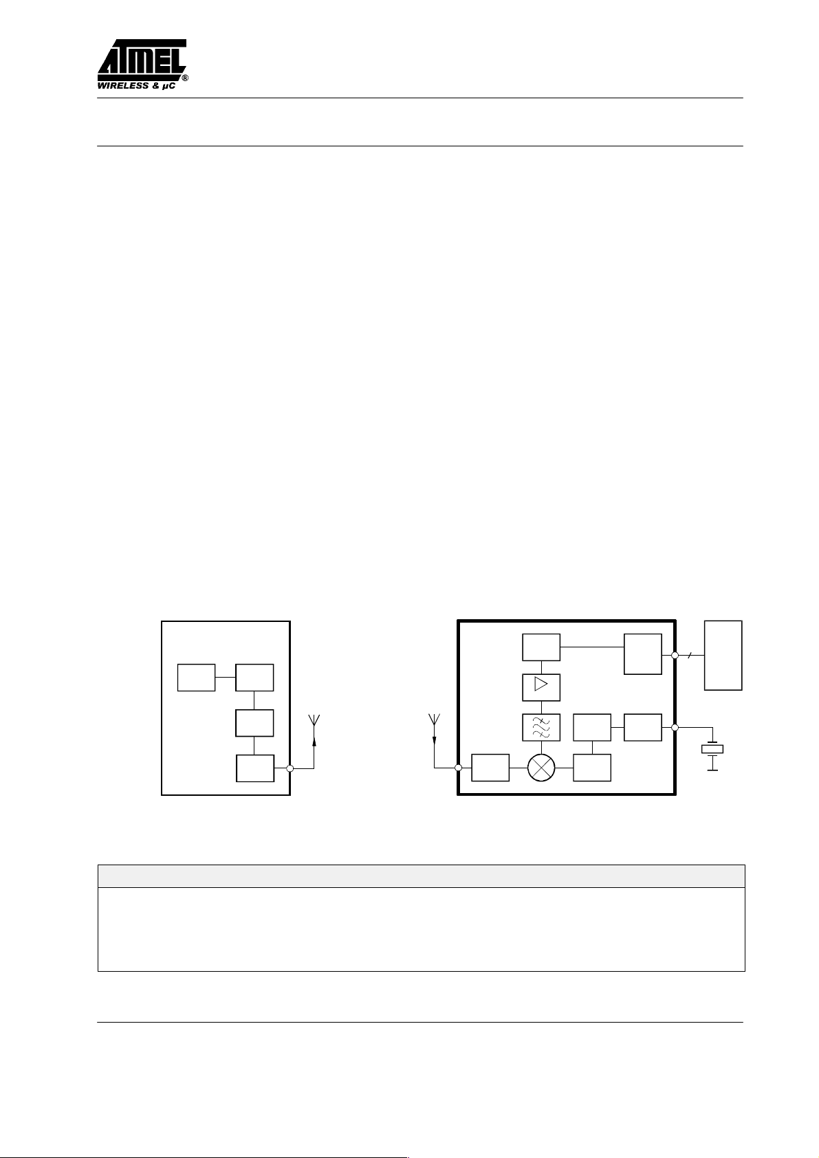
System Block Diagram
UHF ASK/FSK
Remote control transmitter
T5750
XTO
PLL
VCO
Power
amp.
Antenna
D Receiving bandwidth BIF = 600 kHz for low cost
90-ppm crystals
D Low power consumption due to configurable polling
D Temperature range –40°C to 105°C
D ESD protection 2 kV HBM, 200 V MM
D Communication to mC possible via a single
bi-directional data line
D Low-cost solution due to high integration level with
minimum external circuitry requirements
UHF ASK/FSK
Remote control receiver
T5760/
1...5
Antenna
T5761
LNA VCO
Demod.
IF Amp
Control
PLL XTO
mC
Figure 1. System block diagram
Ordering Information
Extended Type Number Package Remarks
T5760-TG SO20 Tube, for 868 MHz ISM band
T5760-TGQ SO20 Taped and reeled, for 868 MHz ISM band
T5761-TG SO20 Tube, for 915 MHz ISM band
T5761-TGQ SO20 Taped and reeled, for 915 MHz ISM band
Rev. A2, 19-Oct-00 1 (32)
Preliminary Information
T5760
T5761/
Pin Description
Pin Symbol Function
1 SENS Sensitivity-control resistor
2 IC_
ACTIVE
3 CDEM Lower cut-off frequency data fil-
4 AVCC Analog power supply
5 TEST 1 Test pin, during operation at GND
6 AGND Analog ground
7 n.c. Not connected, connect to GND
8 LNAREF High-frequency reference node
9 LNA_IN RF input
10 LNAGND DC ground LNA and mixer
11 TEST 2 Do not connect during operating
12 TEST 3 Test pin, during operation at GND
13 n.c. Not connected, connect to GND
14 XTAL Crystal oscillator XTAL connec-
15 DVCC Digital power supply
16 TEST 4 Test pin, during operation at
17 DATA_
CLK
18 DGND Digital ground
19 POLL-
ING/_ON
20 DATA Data output / configuration input
IC condition indicator
Low = sleep mode
High = active mode
ter
LNA and mixer
tion
DVCC
Bit clock of data stream
Selects polling or rceiving mode
Low: receiving mode
High: polling mode
SENS
IC_ACTIVE
CDEM
AVCC
TEST 1
AGND
n.c.
LNAREF
LNA_IN
LNAGND
1
2
3
4
5
T5760/
6
7
10
T5761
8
9
Figure 2. Pinning SO20
20
19
18
17
16
15
14
13
12
11
DATA
POLLING
/_ON
DGND
DATA_CLK
TEST 4
DVCC
XTAL
n.c.
TEST 3
TEST 2
2 (32)
Rev. A2, 19-Oct-00
Preliminary Information
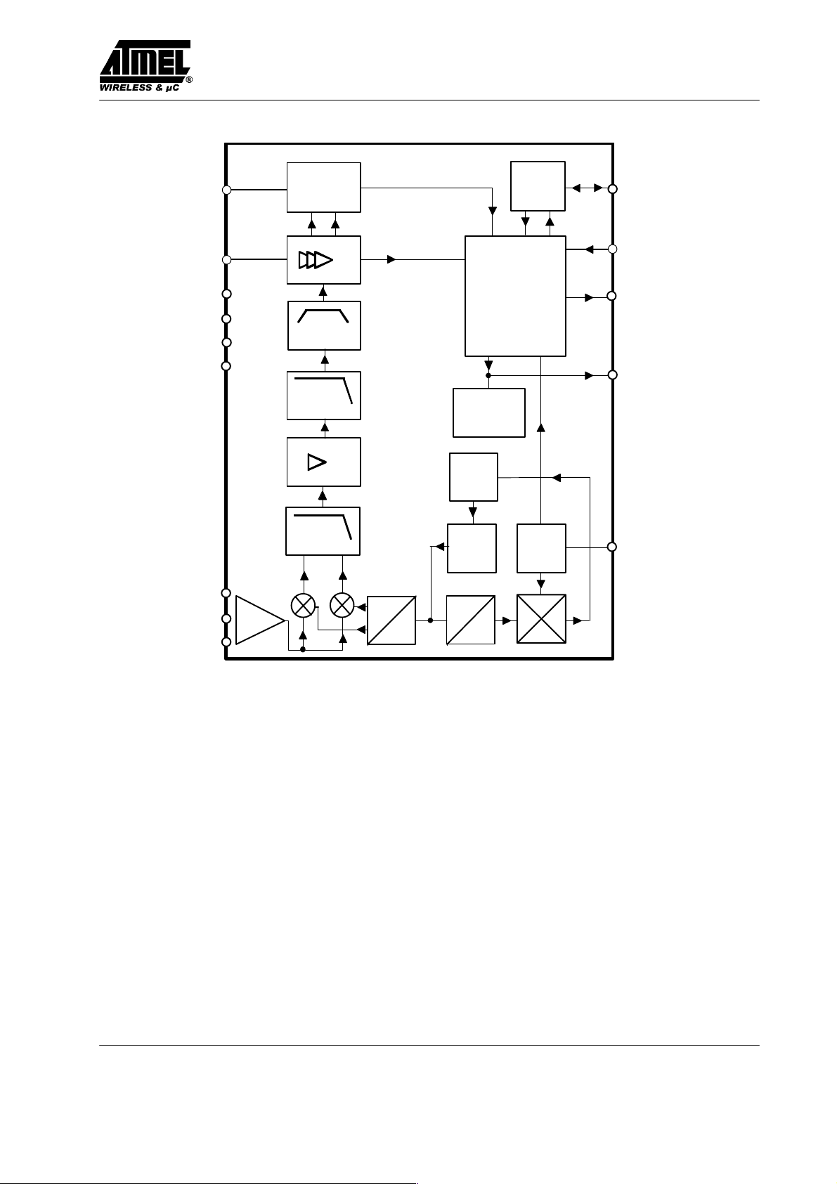
Block Diagram
/
T5761T5760
CDEM
SENS
AVCC
AGND
DGND
DVCC
FSK/ASK–
demodulator
and data filter
Rssi Limiter out
RSSI IF
Amp.
4. Order
f0=950 kHz/
1 MHz
LPF
fg=2.2MHz
IF
Amp.
Poly–LPF
fg=7MHz
Dem_out
Sensitivity–
reduction
Polling circuit
control logic
FE CLK
Standby logic
Loop–
filter
LC–VCO
interface
and
Data –
XTO
DATA
POLLING/_ON
DATA_CLK
IC_ACTIVE
XTAL
LNAREF
LNA_IN
LNA
f
:2
LNAGND
Figure 3. Block diagram
RF Front End
The RF front end of the receiver is a low-IF heterodyne
configuration that converts the input signal into a
950-kHz/ 1-MHz IF signal with an image rejection of typical 30dB. According to figure 3 the front end consists of
an LNA (low noise amplifier), LO (local oscillator), I/Q
mixer, polyphase lowpass filter and an IF amplifier.
The PLL generates the carrier frequency for the mixer via
a full integrated synthesizer with integrated low noise
LC-VCO (voltage controlled oscillator ) and PLL-loopfilter. The XTO ( crystal oscillator ) generates the
reference frequency f
erates two times the mixer drive frequency f
signals for the mixer are generated with a divide by two
circuit ( fLO = f
VCO
and feed into a phase frequency detector and compared
. The integrated LC-VCO gen-
XTO
/2 ). f
is divided by a factor of 256
VCO
VCO
. The I/Q
f
:256
with f
. The output of the phase frequency detector is
XTO
feed into an integrated loopfilter and thereby generates
the control voltage for the VCO. If fLO is determined,
f
can be calculated using the following formula:
XTO
f
= fLO / 128
XTO
The XTO is a one-pin oscillator that operates at the series
resonance of the quartz crystal with high current but low
voltage signal, so that there is only a small voltage at the
crystal oscillator frequency at Pin XTAL. According to
figure 4, the crystal should be connected to GND with a
series capacitor CL. The value of that capacitor is recommended by the crystal supplier. Due to a somewhat
inductive impedance at steady state oscillation and some
PCB parasitics a lower value of CL is normally necessary.
Rev. A2, 19-Oct-00 3 (32)
Preliminary Information
T5760
T5761/
The value of CL should be optimized for the individual
board layout to achieve the exact value of f
XTO
(the best
way is to use a crystal with known load resonance frequency to find the right value for this capacitor) and
hereby of fLO. When designing the system in terms of receiving bandwidth and local oscillator accuracy, the
accuracy of the crystal and the XTO must be considered.
If a crystal with $30 ppm adjustment tolerance at 25_C
, $50ppm over T emperature –40_C to 105_C, $10 ppm
of total aging and a CM ( motional capacitance ) of 7 fF
is used, an additional XTO pulling of $30 ppm has to be
added.
The resulting total LO tolerance of $120ppm agrees with
the receiving bandwidth specification of the
T5760/T5761 if the T5750 has also a total LO tolerance
of $120 ppm.
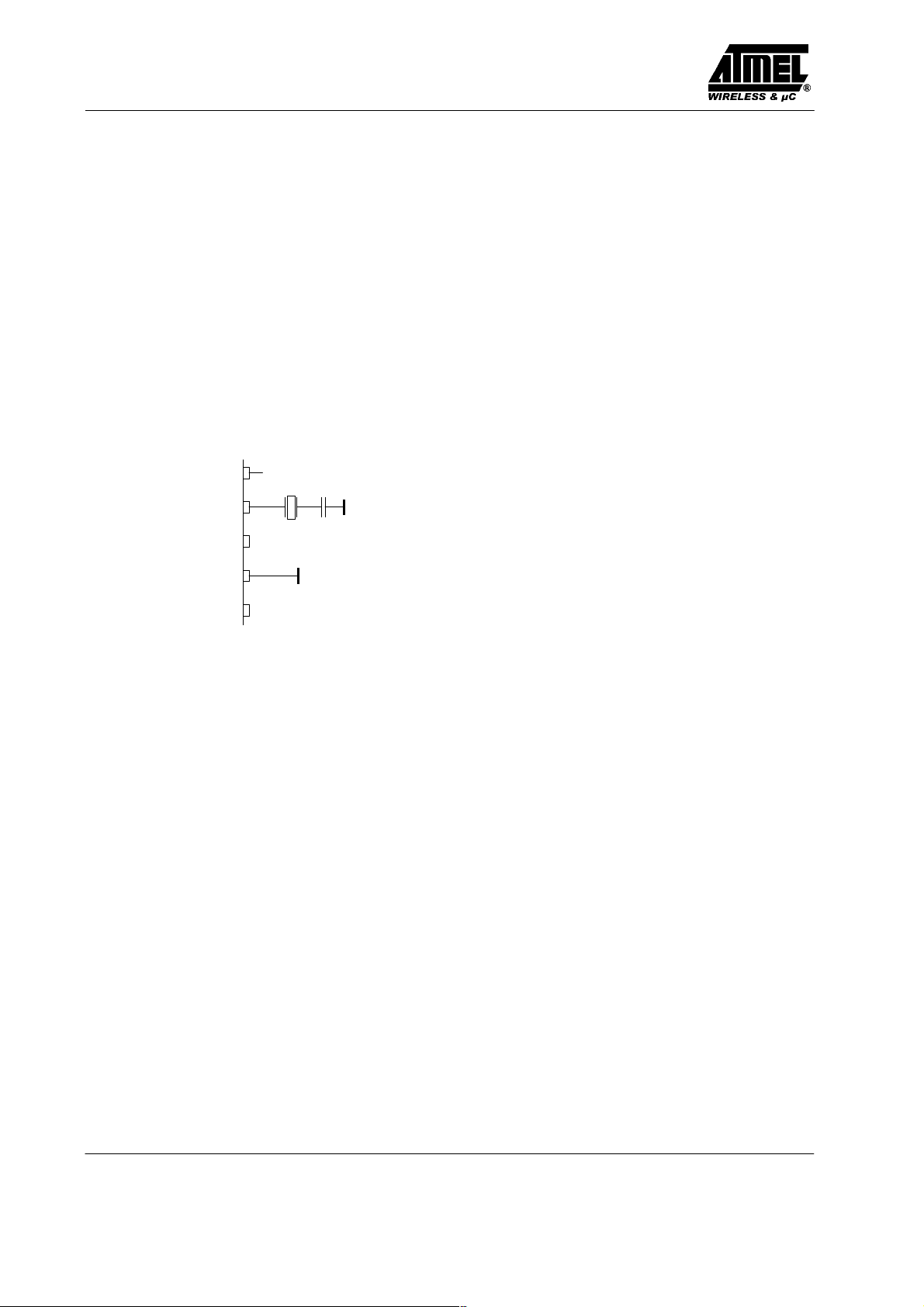
V
n.c.
S
C
L
DVCC
XTAL
TEST 3
TEST 2
Figure 4. XTO peripherals
The nominal frequency fLO is determined by the RF input
frequency fRF and the IF frequency fIF using the following
formula (low side injection):
fLO = fRF – f
IF
To determine fLO , the construction of the IF filter must
be considered at this point. The nominal IF frequency is
fIF = 950 kHz. To achieve a good accuracy of the filter
corner frequencies, the filter is tuned by the crystal frequency f
. This means that there is a fixed relation
XTO
between fIF and fLO.
fIF = fLO / 915
The relation is designed to achieve the nominal IF fre-
quency of fIF = 950 kHz for the 868.3 MHz version. For
the 915 MHz version an IF frequency of fIF = 1.0 MHz
results.
The RF input either from an antenna or from a RF generator must be transformed to the RF input Pin LNA_IN. The
input impedance of that pin is provided in the electrical
parameters. The parasitic board inductances and capacitances influence the input matching. The RF receiver
T5760/T5761 exhibits its highest sensitivity if the LNA
is power matched. This makes the matching to an SAW
filter as well as to 50 W or an antenna more easy.
Figure 33 shows a typical input matching network for f
RF
= 868.3 MHz to 50 W. Figure 34 illustrates an according
input matching for 868.3 MHz to an SAW. The input
matching network shown in Figure 33 is the reference network for the parameters given in the electrical
characteristics.
Analog Signal Processing
IF Filter
The signals coming from the RF front end are filtered by
the fully integrated 4th-order IF filter. The IF center frequency is fIF = 950 kHz for applications where fRF =
868.3 MHz and fIF =1.0 MHz for fRF = 915 MHz. The
nominal bandwidth is 600 kHz.
Limiting RSSI Amplifier
The subsequent RSSI amplifier enhances the output
signal of the IF amplifier before it is fed into the demodulator. The dynamic range of this amplifier is
DR
its linear range, the best S/N ratio is maintained in ASK
mode. If the dynamic range is exceeded by the transmitter
signal, the S/N ratio is defined by the ratio of the maximum RSSI output voltage and the RSSI output voltage
due to a disturber. The dynamic range of the RSSI amplifier is exceeded if the RF input signal is about 60 dB
higher compared to the RF input signal at full sensitivity.
In FSK mode the S/N ratio is not affected by the dynamic
range of the RSSI amplifier, because only the hard limited
signal from a high gain limiting amplifier is used by the
demodulator.
The output voltage of the RSSI amplifier is internally
compared to a threshold voltage V
mined by the value of the external resistor R
connected between Pin SENS and GND or VS. The output
of the comparator is fed into the digital control logic. By
this means it is possible to operate the receiver at a lower
sensitivity.
If R
sensitivity. It is also possible to connect the Pin SENS directly to GND to get the maximum sensitivity.
If R
lower sensitivity. The reduced sensitivity is defined by the
value of R
noise ratio of the LNA input. The reduced sensitivity
depends on the signal strength at the output of the RSSI
amplifier.
Since different RF input networks may exhibit slightly
different values for the LNA gain, the sensitivity values
given in the electrical characteristics refer to a specific
input matching. This matching is illustrated in figure 33
= 60 dB. If the RSSI amplifier is operated within
RSSI
. V
Th_red
is connected to GND, the receiver switches to full
Sens
is connected to VS, the receiver operates at a
Sens
, the maximum sensitivity by the signal-to-
Sens
Th_red
Sens
is deter-
. R
Sens
is
4 (32)
Rev. A2, 19-Oct-00
Preliminary Information

/
T5761T5760
and exhibits the best possible sensitivity and at the same
time power matching at RF_IN.
R
can be connected to VS or GND via a µC. The
Sens
receiver can be switched from full sensitivity to reduced
sensitivity or vice versa at any time. In polling mode, the
receiver will not wake up if the RF input signal does not
exceed the selected sensitivity. If the receiver is already
active, the data stream at Pin DATA will disappear when
the input signal is lower than defined by the reduced
sensitivity. Instead of the data stream, the pattern according to figure 5 is issued at Pin DATA to indicate that the
receiver is still active (see also figure 32).
DATA
t
DATA_min
Figure 5. Steady L state limited DATA output pattern
t
DATA_L_max
FSK/ASK Demodulator and Data Filter
The signal coming from the RSSI amplifier is converted
into the raw data signal by the ASK/FSK demodulator.
The operating mode of the demodulator is set via the bit
ASK/_FSK in the OPMODE register. Logic ‘L’ sets the
demodulator to FSK, applying ‘H’ to ASK mode.
In ASK mode an automatic threshold control circuit
(ATC) is employed to set the detection reference voltage
to a value where a good signal to noise ratio is achieved.
This circuit also implies the effective suppression of any
kind of in-band noise signals or competing transmitters.
If the S/N (ratio to suppress in-band noise signals) exceeds about 10 dB the data signal can be detected
properly, but better values are found for many modulation
schemes of the competing transmitter.
The FSK demodulator is intended to be used for an FSK
deviation of 10 kHz ≤ Df ≤ 100 kHz. In FSK mode the
data signal can be detected if the S/N (ratio to suppress
inband noise signals) exceeds about 2 dB. This value is
valid for all modulation schemes of a disturber signal.
The output signal of the demodulator is filtered by the
data filter before it is fed into the digital signal processing
circuit. The data filter improves the S/N ratio as its passband can be adopted to the characteristics of the data
signal. The data filter consists of a 1st-order highpass and
a 2nd-order lowpass filter
The highpass filter cut-off frequency is defined by an
external capacitor connected to Pin CDEM. The cut-off
frequency of the highpass filter is defined by the following formula:
fcu_DF +
In self-polling mode, the data filter must settle very
rapidly to achieve a low current consumption. Therefore,
CDEM cannot be increased to very high values if selfpolling is used. On the other hand CDEM must be large
enough to meet the data filter requirements according to
the data signal. Recommended values for CDEM are
given in the electrical characteristics.
The cut-off frequency of the lowpass filter is defined by
the selected baud-rate range (BR_Range). The
BR_Range is defined in the OPMODE register (refer to
chapter ‘Configuration of the Receiver’). The BR_Range
must be set in accordance to the used baud-rate.
The T5760/T5761 is designed to operate with data coding
where the DC level of the data signal is 50%. This is valid
for Manchester and Bi-phase coding. If other modulation
schemes are used, the DC level should always remain
within the range of V
The sensitivity may be reduced by up to 2 dB in that
condition.
Each BR_Range is also defined by a minimum and a
maximum edge-to-edge time (t
defined in the electrical characteristics. They should not
be exceeded to maintain full sensitivity of the receiver.
2 p 30 kW CDEM
1
DC_min
= 33% and V
). These limits are
ee_sig
DC_max
= 66%.
Receiving Characteristics
The RF receiver T5760/T5761 can be operated with and
without a SAW front-end filter. In a typical automotive
application, a SAW filter is used to achieve better selectivity and large signal capability. The receiving frequency
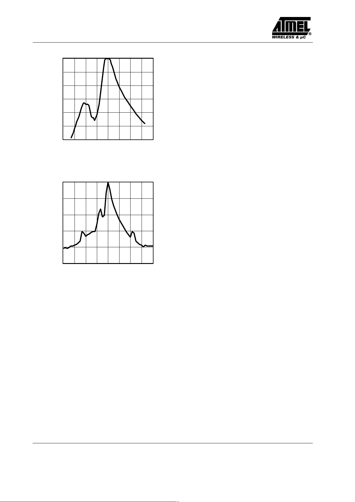
response without a SAW front-end filter is illustrated in
figures 6 and 7. This example relates to ASK mode. FSK
mode exhibit similar behavior. The plots are printed relatively to the maximum sensitivity. If a SAW filter is used,
an insertion loss of about 3 dB must be considered, but the
over all selectivity is much better.
When designing the system in terms of receiving bandwidth, the LO deviation must be considered as it also
determines the IF center frequency. The total LO deviation is calculated to be the sum of the deviation of the
crystal and the XTO deviation of the T5760/T5761. Lowcost crystals are specified to be within ±90 ppm over
tolerance, temperature and aging. The XTO deviation of
the T5760/T5761 is an additional deviation due to the
XTO circuit. This deviation is specified to be ±30 ppm
worst case for a crystal with CM = 7 fF. If a crystal of
±90 ppm is used, the total deviation is ±120 ppm in that
case. Note that the receiving bandwidth and the IF-filter
bandwidth are equivalent in ASK mode but not in FSK
mode.
Rev. A2, 19-Oct-00 5 (32)
Preliminary Information
T5760
T5761/
0
–10
–20
–30
dP ( dB )
–40
–50
–60
–4 –3 –2 –101234
df ( MHz )
Figure 6. Narrow band receiving frequency response
0
–20
–40
dP ( dB )
–60
–80
–100
–12 –9 –6 –3036912
df ( MHz )
Figure 7. Wide band receiving frequency response
Polling Circuit and Control Logic
The receiver is designed to consume less than 1 mA while
being sensitive to signals from a corresponding transmitter. This is achieved via the polling circuit. This circuit
enables the signal path periodically for a short time.
During this time the bit-check logic verifies the presence
of a valid transmitter signal. Only if a valid signal is
detected the receiver remains active and transfers the data
to the connected µC. If there is no valid signal present the
receiver is in sleep mode most of the time resulting in low
current consumption. This condition is called polling
mode. A connected µC is disabled during that time.
All relevant parameters of the polling logic can be configured by the connected µC. This flexibility enables the
user to meet the specifications in terms of current consumption, system response time, data rate etc.
Regarding the number of connection wires to the mC, the
receiver is very flexible. It can be either operated by a
single bi-directional line to save ports to the connected mC
or it can be operated by up to five uni-directional ports.
Basic Clock Cycle of the Digital Circuitry
The complete timing of the digital circuitry and the
analog filtering is derived from one clock. This clock
cycle T
is derived from the crystal oscillator (XTO) in
Clk
combination with a divide by 14 circuit. According to
chapter ‘RF Front End’, the frequency of the crystal oscillator (f
) is defined by the RF input signal (f
XTO
RFin
) which
also defines the operating frequency of the local oscillator
(fLO). The basic clock cycle is T
T
= 2.066 ms for f
Clk
T
= 1.961 ms for f
Clk
T
controls the following application-relevant parame-
Clk
= 915 MHz
RF
= 14/ f
Clk
= 868.3 MHz and
RF
XTO
giving
ters:
D Timing of the polling circuit including bit check
D Timing of the analog and digital signal processing
D Timing of the register programming
D Frequency of the reset marker
D IF filter center frequency (f
IF0
)
Most applications are dominated by two transmission frequencies: f
f
= 868.3 MHz in Europe. In order to ease the
Transmit
usage of all T
= 915 MHz is mainly used in USA,
Transmit
-dependent parameters on this electrical
Clk
characteristics display three conditions for each parameter.
D Application USA
(f
= 7.14063 MHz, T
XTO
= 1.961 µs)
Clk
D Application Europe
(f
= 6.77617 MHz, T
XTO
= 2.066 µs)
Clk
D Other applications
The electrical characteristic is given as a function of
T
.
Clk
The clock cycle of some function blocks depends on the
selected baud-rate range (BR_Range) which is defined in
the OPMODE register. This clock cycle T
XClk
is defined
by the following formulas for further reference:
BR_Range = BR_Range0: T
BR_Range1: T
BR_Range2: T
BR_Range3: T
XClk
XClk
XClk
XClk
= 8 × T
= 4 × T
= 2 × T
= 1 × T
Clk
Clk
Clk
Clk
Polling Mode
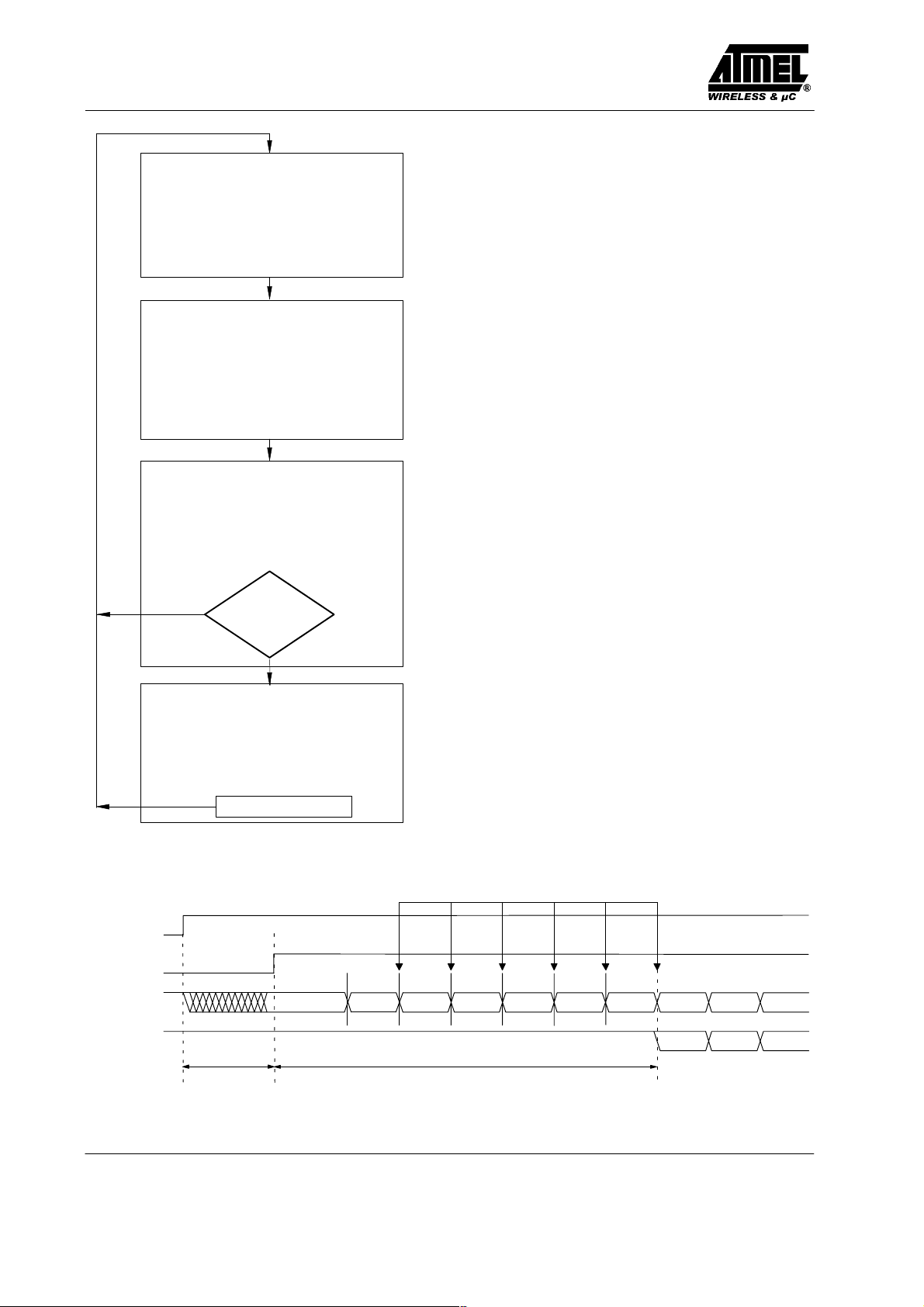
According to figure 11, the receiver stays in polling mode
in a continuous cycle of three different modes. In sleep
mode the signal processing circuitry is disabled for the
time period T
IS = I
. During the start-up period, T
Soff
processing circuits are enabled and settled. In the follow-
while consuming low current of
Sleep
Startup
, all signal
6 (32)
Rev. A2, 19-Oct-00
Preliminary Information

/
T5761T5760
ing bit-check mode, the incoming data stream is analyzed
bit by bit contra a valid transmitter signal. If no valid
signal is present, the receiver is set back to sleep mode after the period T
Bit-check
. This period varies check by
check as it is a statistical process. An average value for
T
Bit-check
T
Startup
is given in the electrical characteristics. During
and T
Bit-check
the current consumption is IS = I
Son
The condition of the receiver is indicated on Pin IC_ACTIVE. The average current consumption in polling mode
is dependent on the duty cycle of the active mode and can
be calculated as:
I
+
I
Spoll
During T
Soff
Sleep
T
Sleep
T
Sleep
and T
) I
(T
Son
) T
Startup
the receiver is not sensitive to
Startup
Startup
) T
) T
Bitcheck
Bitcheck
)
a transmitter signal. To guarantee the reception of a transmitted command the transmitter must start the telegram
with an adequate preburst. The required length of the
preburst depends on the polling parameters T
T
(T
and the number of bits (N
Startup
Start,µC
, T
Bit-check
). Thus, T
and the start-up time of a connected µC
Bit-check
depends on the actual bit rate
Bit-check
) to be tested.
Sleep
The following formula indicates how to calculate the
preburst length.
T
Preburst
w T
Sleep
+ T
Startup
+ T
Bit-check
+ T
Start_mC
Sleep Mode
The length of period T
.
Sleep of the OPMODE register, the extension factor
is defined by the 5-bit word
Sleep
XSleep (according to table 9), and the basic clock cycle
T
. It is calculated to be:
Clk
T
= Sleep X
Sleep
1024 T
Sleep
Clk
In US- and European applications, the maximum value of
T
is about 60 ms if XSleep is set to 1. The time reso-
Sleep
lution is about 2 ms in that case. The sleep time can be
extended to almost half a second by setting XSleep to 8.
XSleep can be set to 8 by bit XSleep
Std
to’1’.
According to table 8, the highest register value of sleep
sets the receiver into a permanent sleep condition. The receiver remains in that condition until another value for
,
Sleep is programmed into the OPMODE register. This
function is desirable where several devices share a single
data line and may also be used for µC polling – via Pin
POLLING/_ON, the receiver can be switched on and off.
Rev. A2, 19-Oct-00 7 (32)
Preliminary Information
T5760
T5761/
Sleep mode:
All circuits for signal processing are
disabled. Only XTO and Polling logic is
enabled.
Output level on Pin IC_ACTIVE => low
= I
I
S
Soff
T
= Sleep × X
Sleep
× 1024 × T
Sleep
Start-up mode:
The signal processing circuits are enabled.
After the start-up time (T
Startup
are in stable condition and ready to receive.
Output level on Pin IC_ACTIVE => high
= I
I
S
Son
T
Startup
Bit-check mode:
The incomming data stream is analyzed. If
the timing indicates a valid transmitter
signal, the receiver is set to receiving mode.
Otherwise it is set to Sleep mode.
Output level on Pin IC_ACTIVE => high
= I
I
S
Son
T
Bit-check
Bit check
NO
OK ?
YES
Receiving mode:
The receiver is turned on permanently and
passes the data stream to the connected mC.
It can be set to Sleep mode through an OFF
command via Pin DATA or POLLING/_ON.
Output level on Pin IC_ACTIVE => high
= I
I
S
Son
OFF command
Clk
) all circuits
Sleep: 5-bit word defined by Sleep0 to
Sleep4 in OPMODE register
X
: Extension factor defined by
Sleep
XSleep
Std
according to table 9
: Basic clock cycle defined by f
T
Clk
and Pin MODE
: Is defined by the selected baud rate
T
Startup
range and T
. The baud-rate range
Clk
is defined by Baud0 and Baud1 in
the OPMODE register.
T
Bit-check:
Depends on the result of the
bit check
If the bit check is ok, T
Bit-check
depends on the number of bits to be
checked (N
Bit-check
) and on the
utilized data rate.
If the bit check fails, the average
time period for that check depends
on the selected baud-rate range and
. The baud-rate range is
on T
Clk
defined by Baud0 and Baud1 in the
OPMODE register.
XTO
( Number of checked Bits: 3 )
IC_ACTIVE
Bit check
Dem_out
Data_out (DATA)
T
Start–up mode
8 (32)
Start–up
Figure 8. Polling mode flow chart
Bit check ok
1/2 Bit
1/2 Bit
T
Bit–check
Bit–check mode
1/2 Bit 1/2 Bit 1/2 Bit 1/2 Bit
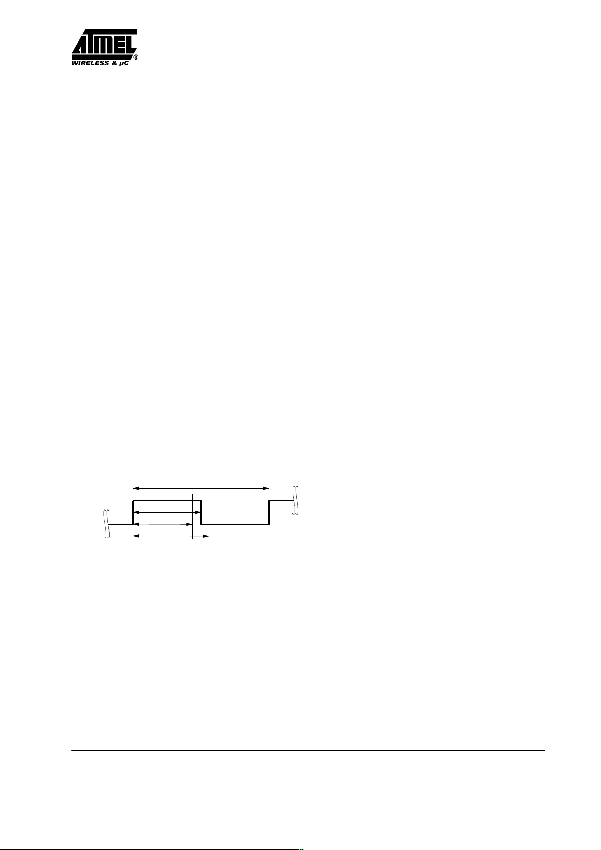
Figure 9. Timing diagram for complete successful bit check
Preliminary Information
Receiving mode
Rev. A2, 19-Oct-00
/
T5761T5760
Bit-Check Mode
In bit-check mode the incoming data stream is examined
to distinguish between a valid signal from a corresponding transmitter and signals due to noise. This is done by
subsequent time frame checks where the distances between 2 signal edges are continuously compared to a
programmable time window. The maximum count of this
edge-to-edge tests before the receiver switches to receiving mode is also programmable.
Configuring the Bit Check
Assuming a modulation scheme that contains 2 edges per
bit, two time frame checks are verifying one bit. This is
valid for Manchester, Bi-phase and most other modulation schemes. The maximum count of bits to be checked
can be set to 0, 3, 6 or 9 bits via the variable N
Bit-check
in
the OPMODE register. This implies 0, 6, 12 and 18 edge
to edge checks respectively. If N
Bit-check
is set to a higher
value, the receiver is less likely to switch to receiving
mode due to noise. In the presence of a valid transmitter
signal, the bit check takes less time if N
Bit-check
is set to
a lower value. In polling mode, the bit-check time is not
dependent on N
Bit-check
. Figure 12 shows an example
where 3 bits are tested successfully and the data signal is
transferred to Pin DATA.
According to figure 13, the time window for the bit check
is defined by two separate time limits. If the edge-to-edge
time tee is in between the lower bit-check limit T
and the upper bit-check limit T
Lim_max
continued. If tee is smaller than T
T
Lim_max
, the bit check will be terminated and the re-
, the check will be
Lim_min
or t
Lim_min
exceeds
ee
ceiver switches to sleep mode.
1/f
Sig
t
Dem_out
Figure 10. Valid time window for bit check
T
Lim_min
T
Lim_max
ee
For best noise immunity it is recommended to use a low
span between T
Lim_min
and T
Lim_max
. This is achieved us-
ing a fixed frequency at a 50% duty cycle for the
transmitter preburst. A ‘11111...’ or a ‘10101...’ sequence
in Manchester or Bi-phase is a good choice concerning
that advice. A good compromise between receiver sensitivity and susceptibility to noise is a time window of
± 25% regarding the expected edge-to-edge time tee. Us-
ing pre-burst patterns that contain various edge-to-edge
time periods, the bit-check limits must be programmed
according to the required span.
The bit-check limits are determined by means of the formula below.
T
Lim_min
T
Lim_max
= Lim_min × T
XClk
= (Lim_max –1) × T
XClk
Lim_min and Lim_max are defined by a 5-bit word each
within the LIMIT register.
Using above formulas, Lim_min and Lim_max can be determined according to the required T
and T
T
Lim_max
(t
DATA_L_min
. The time resolution defining T
XClk
is T
. The minimum edge-to-edge time t
XClk
, t
DATA_H_min
) is defined according to the
Lim_min
, T
Lim_max
Lim_min
and
chapter ‘Receiving Mode’. The lower limit should be set
to Lim_min ≥ 10. The maximum value of the upper limit
is Lim_max = 63.
If the calculated value for Lim_min is < 19, it is recommended to check 6 or 9 bits (N
Bit-check
) to prevent
switching to receiving mode due to noise.
Figures 14, 15 and 16 illustrate the bit check for the bit-
check limits Lim_min = 14 and Lim_max = 24. When
the IC is enabled, the signal processing circuits are enabled during T
. The output of the ASK/ FSK
Startup
demodulator (Dem_out) is undefined during that period.
When the bit check becomes active, the bit-check counter
is clocked with the cycle T
XClk
.
Figure 14 shows how the bit check proceeds if the bitcheck counter value CV_Lim is within the limits defined
by Lim_min and Lim_max at the occurrence of a signal
edge. In figure 15 the bit check fails as the value CV_lim
is lower than the limit Lim_min. The bit check also fails
if CV_Lim reaches Lim_max. This is illustrated in
figure 16.
ee
Rev. A2, 19-Oct-00 9 (32)
Preliminary Information
T5760
T5761/
( Lim_min = 14, Lim_max = 24 )
IC_ACTIVE
Bit check
Dem_out
Bit–check–
counter
( Lim_min = 14, Lim_max = 24 )
IC_ACTIVE
Bit check
Dem_out
Bit–check–
counter
0
T
Start–up
Start–up mode
0
T
Start–up
Start–up mode
3456 245
2
1
7 81 36789111213
T
XClk
Figure 11. Timing diagram during bit check
1/2 Bit
23456 2451 1 3 6789 111210
T
Bit–check
Bit–check mode
Bit check ok
1/2 Bit
10
T
Bit–check
Bit–check mode
Bit check failed ( CV_Lim < Lim_min )
17 18123456
14
15 16
0
T
Sleep mode
Sleep
Bit check ok
1/2 Bit 1/2 Bit
78910111213
14 15
1234
Figure 12. Timing diagram for failed bit check (condition: CV_Lim < Lim_min)
( Lim_min = 14, Lim_max = 24 )
IC_ACTIVE
Bit check
Dem_out
Bit–check–
counter
0
T
Start–up
Start–up mode
23456 245
1 7 36789
1
T
Bit–check
Bit–check mode
Figure 13. Timing diagram for failed bit check (condition: CV_Lim >= Lim_max)
Duration of the Bit Check
If no transmitter signal is present during the bit check, the
output of the ASK/ FSK demodulator delivers random
signals. The bit check is a statistical process and T
Bit-check
varies for each check. Therefore, an average value for
T
Bit-check
T
Bit-check
T
Clk
T
Bit-check
is given in the electrical characteristics.
depends on the selected baud-rate range and on
. A higher baud-rate range causes a lower value for
resulting in a lower current consumption in pol-
ling mode.
In the presence of a valid transmitter signal, T
dependent on the frequency of that signal, f
count of the checked bits, N
Bit-check
. A higher value for
Bit-check
Sig
is
, and the
Bit check failed ( CV_Lim >= Lim_max )
1/2 Bit
11 1210
N
Bit-check
14 15 161718 19 21 22 23 24
13
thereby results in a longer period for T
20
0
T
Sleep
Sleep mode
Bit-check
requiring a higher value for the transmitter pre-burst
T
Preburst
.
Receiving Mode
If the bit check was successful for all bits specified by
N
Bit-check
, the receiver switches to receiving mode. According to figure 9, the internal data signal is switched to
Pin DATA in that case and the data clock is available after
the start bit has been detected (figure 20). A connected µC
can be woken up by the negative edge at Pin DATA or by
the data clock at Pin DATA_CLK. The receiver stays in
that condition until it is switched back to polling mode explicitly.
10 (32)
Rev. A2, 19-Oct-00
Preliminary Information

/
T5761T5760
Digital Signal Processing
The data from the ASK/ FSK demodulator (Dem_out) is
digitally processed in different ways and as a result converted into the output signal data. This processing
depends on the selected baud-rate range (BR_Range).
Figure 14 illustrates how Dem_out is synchronized by the
extended clock cycle T
. This clock is also used for the
XClk
bit-check counter. Data can change its state only after
T
has elapsed. The edge-to-edge time period tee of the
XClk
Data signal as a result is always an integral multiple of
T
.
XClk
The minimum time period between two edges of the data
T
XClk
Clock bit–check
counter
Dem_out
Data_out (DATA)
Figure 14. Synchronization of the demodulator output
t
ee
signal is limited to tee ≥ T
DATA_min
. This implies an efficient suppression of spikes at the DATA output. At the
same time it limits the maximum frequency of edges at
DATA. This eases the interrupt handling of a connected
µC.
The maximum time period for DATA to stay Low is limited to T
DATA_L_max
. This function is employed to ensure
a finite response time in programming or switching off the
receiver via Pin DATA. T
DATA_L_max
is thereby longer
than the maximum time period indicated by the transmitter data stream. Figure 16 gives an example where
Dem_out remains Low after the receiver has switched to
receiving mode.
Dem_out
Data_out (DATA)
IC_ACTIVE
Bit check
Dem_out
Data_out (DATA)
t
DATA_min
Start–up mode
t
DATA_min
t
ee
Figure 15. Debouncing of the demodulator output
Bit–check mode
t
ee
Receiving mode
t
DATA_min
t
DATA_min
t
DATA_L_max
t
ee
Figure 16. Steady L state limited DAT A output pattern after transmission
Rev. A2, 19-Oct-00 11 (32)
Preliminary Information

T5760
T5761/
After the end of a data transmission, the receiver remains
active. Depending of the bit Noise_Disable in the OPMODE register, the output signal at Pin DATA is high or
random noise pulses appear at Pin DATA (see chapter
’Digital Noise Supression’). The edge-to-edge time period tee of the majority of these noise pulses is equal or
slightly higher than T
DATA_min
.
Switching the Receiver Back to Sleep Mode
The receiver can be set back to polling mode via Pin
DATA or via Pin POLLING/_ON.
When using Pin DATA, this pin must be pulled to Low for
the period t1 by the connected µC. Figure 17 illustrates
the timing of the OFF command (see also figure 32). The
IC_ACTIVE
Out1 (µC)
Data_out (DATA)
X
t1 t2 t3
t5
t4
t10
t7
minimum value of t1 depends on BR_Range. The maximum value for t1 is not limited but it is recommended not
to exceed the specified value to prevent erasing the reset
marker. Note also that an internal reset for the OPMODE
and the LIMIT register will be generated if t1 exceeds the
specified values. This item is explained in more detail in
the chapter ‘Configuration of the Receiver ’. Setting the
receiver to sleep mode via DATA is achieved by programming bit 1 to be ‘1’ during the register configuration. Only
one sync pulse (t3) is issued.
The duration of the OFF command is determined by the
sum of t1, t2 and t10. After the OFF command the sleep
time T
elapses. Note that the capacitive load at Pin
Sleep
DATA is limited (see chapter ’Data Interface’).
Serial bi–directional
data line
IC_ACTIVE
POLLING/_ON
Data_out (DATA)
Serial bi–directional
data line
X
Receiving
mode
Bit 1
(”1”)
(Start bit)
OFF–command
Figure 17. Timing diagram of the OFF-command via Pin DATA
t
on2
X
X
Receiving mode
t
on3
Sleep mode Start–up mode Bit–check mode Receiving mode
T
Sleep
Sleep mode
Bit check ok
T
Start–up
Start–up mode
X
X
12 (32)
Figure 18. Timing diagram of the OFF-command via Pin POLLING/_ON
Rev. A2, 19-Oct-00
Preliminary Information

IC_ACTIVE
POLLING/_ON
/
T5761T5760
t
on1
Data_out (DATA)
Serial bi–directional
data line
Sleep mode Receiving mode
Figure 19. Activating the receiving mode via Pin POLLING/_ON
Figure 18 illustrates how to set the receiver back to polling mode via Pin POLLING/_ON. The Pin
POLLING/_ON must be held to low for the time period
t
. After the positive edge on Pin POLLING/_ON and
on2
the delay t
time T
Sleep
, the polling mode is active and the sleep
on3
elapses.
This command is faster than using Pin DATA at the cost
of an additional connection to the µC.
Figure 19 illustrates how to set the receiver to receiving
mode via the Pin POLLING/_ON. The Pin POLLING/_ON must be held to Low. After the delay t
on1
, the
receiver changes from sleep mode to start–up mode regardless the programmed values for T
Sleep
and N
Bit–check
As long as POLLING/_ON is held to Low, the values for
T
Sleep
and N
Bit–check
will be ignored, but not deleted (see
also chapter ’Digital Noise Suppression’).
If the receiver is polled exclusively by a µC, T
Sleep
must
be programmed to 31 (permanent sleep mode). In this
case the receiver remains in sleep mode as long as POLLING/_ON is held to High.
Data Clock
The Pin DATA_CLK makes a data shift clock available
to sample the data stream into a shift register. Using this
data clock, a µC can easily synchronize the data stream.
This clock can only be used for Manchester and Bi-
phase coded signals.
Generation of the data clock:
After a successful bit check, the receiver switches from
polling mode to receiving mode and the data stream is
available at Pin DATA. In receiving mode, the data clock
control logic (Manchester/Bi-phase demodulator) is active and examines the incoming data stream. This is done,
like in the bit check, by subsequent time frame checks
where the distance between two edges is continuously
X
X
Start–up mode
compared to a programmable time window. As illustrated
in figure 20, only two distances between two edges in
Manchester and Bi-phase coded signals are valid (T and
2T).
The limits for T are the same as used for the bit check.
They can be programmed in the LIMIT-register
(Lim_min and Lim_max, see tables 10 and 11).
The limits for 2T are calculated as follows:
Lower limit of 2T:
Lim_min_2T = (Lim_min + Lim_max) – (Lim_max – Lim_min) / 2
Upper limit of 2T:
.
Lim_max_2T= (Lim_min + Lim_max) + (Lim_max – Lim_min) / 2
(If the result for ’Lim_min_2T’ or ’Lim_max_2T’ is not
an integer value, it will be round up)
The data clock is available, after the data clock control
logic has detected the distance 2T (Start bit) and is issued
with the delay t
after the edge on Pin DATA (see fig-
Delay
ure 20).
If the data clock control logic detects a timing or logical
error (Manchester code violation), like illustrated in figures 21 and 22, it stops the output of the data clock. The
receiver remains in receiving mode and starts with the bit
check. If the bit check was successful and the start bit has
been detected, the data clock control logic starts again
with the generation of the data clock (see figure 23).
It is recommended to use the function of the data clock
only in conjunction with the bit check 3, 6 or 9. If the bit
check is set to 0 or the receiver is set to receiving mode
via the Pin POLLING/_ON, the data clock is available if
the data clock control logic has detected the distance 2T
(Start bit).
Note that for Bi-phase-coded signals, the data clock is issued at the end of the bit.
Rev. A2, 19-Oct-00 13 (32)
Preliminary Information

T5760
T5761/
Preburst Data
Dem_out
Data_out (DATA)
DATA_CLK
Dem_out
Data_out (DATA)
Bit check ok
’1’ ’1’’1’’1’’1’ ’0’’1’’1’’0’’1’’0’
Bit–check mode
T2T
Start bit
t
Receiving mode,
data clock control logic active
Delay
t
P_Data_Clk
Figure 20. Timing diagram of the data clock
Data
Timing error
’1’ ’1’’1’’1’’1’ ’0’’1’’1’’0’’1’’0’
(Tee < T
T
ee
Lim_min
OR T
Lim_max
<Tee< T
Lim_min_2T
OR Tee > T
Lim_max_2T
)
DATA_CLK
Dem_out
Data_out (DATA)
DATA_CLK
Receiving mode,
data clock control
logic active
Receiving mode,
bit check active
Figure 21. Data clock disappears because of a timing error
Data
Logical error (Manchester code violation)
’1’ ’1’’1’’0’’1’ ’1’’?’’0’’0’’1’’0’
Receiving mode,
data clock control
logic active
Receiving mode,
bit check aktive
Figure 22. Data clock disappears because of a logical error
14 (32)
Rev. A2, 19-Oct-00
Preliminary Information

Dem_out
Data_out (DATA)
DATA_CLK
/
T5761T5760
Data
Bit check ok
’1’ ’1’’1’’1’’1’ ’0’’1’’1’’0’’1’’0’
Receiving mode,
bit check active
Start bit
Receiving mode,
data clock control
logic active
Figure 23. Output of the data clock after a successful bit check
The delay of the data clock is calculated as follows:
t
= t
Delay
t
is the delay between the internal signals Data_Out
Delay1
and Data_In. For the rising edge, t
Delay1
+ t
Delay2
depends on the
Delay1
capacitive load CL at Pin DATA and the external pull–up
resistor R
tionally on the external voltage V
. For the falling edge, t
pup
Data_Out
Serial bi–directional
data line
Data_In
DAT A_CLK
Figure 24. Timing characteristic of the data clock (rising edge on Pin DATA)
depends addi-
Delay1
(see figures 24, 25 and
X
V
X
= 0,65 * V
V
Ih
V
Il
= 0,35 * V
S
S
32). When the level of Data_In is equal to the level of
Data_Out, the data clock is issued after an additional
delay t
Delay2
.
Note that the capacitive load at Pin DATA is limited. If the
maximum tolerated capacitive load at Pin DATA is exceeded, the data clock disappears (see chapter ’Data
Interface’).
t
t
Delay1
Delay2
t
t
Delay
P_Data_Clk
Data_Out
V
X
VIh = 0,65 * VS
Serial bi–directional
data line
Data_In
DATA_CLK
t
Delay1
t
Delay
t
Delay2
t
VIl = 0,35 * VS
P_Data_Clk
Figure 25. Timing characteristic of the data clock (falling edge of the Pin DATA)
Rev. A2, 19-Oct-00 15 (32)
Preliminary Information

T5760
T5761/
Digital Noise Suppression
After a data transmission, digital noise appears on the data
output (see figure 26). To prevent that digital noise keeps
the connected µC busy, it can be suppressed in two different ways.
1. Automatic noise suppression:
If the bit Noise_Disable (table 9) in the OPMODE register
is set to 1 (default), the receiver changes to bit-check
mode at the end of a valid data stream. The digital noise
Bit check ok
Data_out (DATA)
DATA_CLK
Bit–check
mode
Preburst Data Digital Noise Preburst Data Digital NoiseDigital Noise
Receiving mode,
data clock control
logic active
Receiving mode,
bit check aktive
Figure 26. Output of digital noise at the end of the data stream
is suppressed and the level at Pin DATA is High in that
case. The receiver changes back to receiving mode, if the
bit check was successful.
This way to suppress the noise is recommended if the data
stream is Manchester or Bi-phase coded and is active after
power on.
Figure 28 illustrates the behavior of the data output at the
end of a data stream. Note that if the last period of the data
stream is a high period (rising edge to falling edge), a
pulse occurs on Pin DATA. The length of the pulse
depends on the selected baud-rate range.
Bit check ok
Receiving mode,
data clock control
logic active
Receiving mode,
bit check aktive
Data_out (DATA)
DATA_CLK
Bit–check
mode
Dem_out
Data_out (DATA)
DATA_CLK
Bit check ok Bit check ok
Preburst Data Preburst Data
Receiving mode,
data clock control
logic active
Bit–check
mode
Figure 27. Automatic noise suppression
Timing error
Data stream Digital noise
’1’ ’1’’1’
data clock control
logic active
(tee < T
T
ee
Lim_min
OR T
Lim_max
T
Pulse
< tee < T
Lim_min_2T
Bit–check modeReceiving mode,
Receiving mode,
data clock control
logic active
OR tee > T
Lim_max_2T
Bit–check
mode
)
16 (32)
Figure 28. Occurence of a pulse at the end of the data stream
Rev. A2, 19-Oct-00
Preliminary Information

2. Controlled noise suppression by the µC:
/
T5761T5760
Bit check ok Bit check ok
Serial bi–directional
data line
(DATA_CLK)
POLLING/_ON
Bit–check
mode
If the bit Noise_Disable (see table 9) in the OPMODE register is set to 0, digital noise appears at the end of a valid
data stream. To suppress the noise, the Pin POLLING/_ON must be set to Low. The receiver remains in
receiving mode. Then, the OFF-command causes the
change to the start-up mode. The programmed sleep time
(see table 7) will not be executed because the level at Pin
POLLING/_ON is low, but the bit check is active in that
case. The OFF-command activates the bit check also if
the Pin POLLING/_ON is held to Low. The receiver
changes back to receiving mode if the bit check was successful. T o activate the polling mode at the end of the data
transmission, the Pin POLLING/_ON must be set to High.
This way to suppress the noise is recommended if the data
stream is not Manchester or Bi-phase coded.
Preburst Data Digital Noise Preburst Data Digital Noise
Receiving mode
OFF–command
Figure 29. Controlled noise suppression
Configuration of the Receiver
Start–up
mode
Bit–check
mode
is operated in default mode, there is no need to program
the registers. Table 3 shows the structure of the registers.
According to table 2 bit 1 defines if the receiver is set
back to polling mode via the OFF command (see chapter
’Receiving Mode’) or if it is programmed. Bit 2 represents the register address. It selects the appropriate
register to be programmed. To get a high programming
reliability, Bit15 (Stop bit), at the end of the programming
operation, must be set to 0.
Table 1 Effect of Bit 1 and Bit 2 on programming the registers
Bit 1 Bit 2 Action
1 x The receiver is set back to polling
mode (OFF command)
0 1 The OPMODE register is pro-
grammed
0 0 The LIMIT register is programmed
Receiving mode
Sleep
mode
The T5760/T5761 receiver is configured via two 12-bit
RAM registers called OPMODE and LIMIT. The registers can be programmed by means of the bidirectional
DATA port. If the register contents have changed due to
a voltage drop, this condition is indicated by a certain output pattern called reset marker (RM). The receiver must
be reprogrammed in that case. After a power-on reset
(POR), the registers are set to default mode. If the receiver
Rev. A2, 19-Oct-00 17 (32)
Table 2 Effect of Bit 15 on programming the register
Bit 15 Action
0 The values will be written into the
register (OPMODE or LIMIT)
1 The values will not be written into the
register
Preliminary Information

T5760
É
É
É
É
É
É
É
É
É
É
ÉÉÉ
É
É
É
É
É
É
É
É
É
É
É
É
É
É
É
É
É
É
É
É
É
É
É
ÉÉÉ
É
É
É
É
É
É
É
É
É
É
É
É
T5761/
Table 3 Effect of the configuration words within the registers
Bit 1 Bit 2 Bit 3 Bit 4 Bit 5 Bit 6 Bit 7 Bit 8 Bit 9 Bit 10 Bit 11 Bit 12 Bit 13 Bit 14 Bit 15
OFF–command
1
OPMODE register
BR_Range N
Bit–check
Modu-
lation
Sleep X
Sleep
Noise
Suppres-
sion
0 1 Baud1 Baud0 BitChk1BitChk0ASK/_
Default
ÉÉ
values of
0
É
É
0
É
0
É
1
É
Sleep4 Sleep3 Sleep2 Sleep1 Sleep0 X
FSK
0
É
0
É
0
É
1
É
1
0
ÉÉ
Sleep
Std
0
ÉÉ
Noise_D
isable
1
É
0
É
Bit 3...14
LIMIT register
Lim_min Lim_max
0 0 Lim_
min5
Default
ÉÉ
values of
Bit 3...14
ÉÉ
0
É
É
Lim_
min4
1
É
É
Lim_
min3
0
É
É
Lim_
min2
1
É
É
Lim_
min1
0
É
É
Lim_
min0
1
É
É
Lim_
max5
1
É
É
Lim_
max4
0
É
É
Lim_
max3
1
É
É
Lim_
max2
0
ÉÉ
ÉÉ
Lim_
max1
0
ÉÉ
ÉÉ
Lim_
max0
1
É
É
0
É
É
The following tables illustrate the effect of the individual configuration words. The default configuration is highlighted
for each word.
BR_Range sets the appropriate baud–rate range and simultaneously defines XLim. XLim is used to define the bit–
check limits T
Table 4 Effect of the configuration word BR_Range
BR_Range Baud-Rate Range / Extension Factor for Bit-Check Limits (XLim)
Baud1 Baud0
0
ÉÉÉÉ
ÉÉÉÉ
0 1 BR_Range1 (application USA / Europe: BR_Range1 = 1.8 kBaud to 3.2 kBaud)
1 0 BR_Range2 (application USA / Europe: BR_Range2 = 3.2 kBaud to 5.6 kBaud)
1 1 BR_Range3 (Application USA / Europe: BR_Range3 = 5.6 kBaud to 10 kBaud)
Lim_min
and T
Lim_max
0
ÉÉÉ
ÉÉÉ
as shown in table 10 and table 11.
BR_Range0 (application USA / Europe: BR_Range0 = 1.0 kBaud to 1.8 kBaud) (De-
ЙЙЙЙЙЙЙЙЙЙЙЙЙЙЙЙЙЙЙЙЙ
fault)
ЙЙЙЙЙЙЙЙЙЙЙЙЙЙЙЙЙЙЙЙЙ
XLim = 8 (Default)
XLim = 4
XLim = 2
XLim = 1
Table 5 Effect of the configuration word N
N
Bit-check
BitChk1 BitChk0
0 0 0
0
1 0 6
1 1 9
18 (32)
Bit-check
Number of Bits to be Checked
1
Preliminary Information
3 (Default)
Rev. A2, 19-Oct-00

Table 6 Effect of the configuration bit Modulation
Modulation
Selected Modulation
ASK/_FSK
0
FSK
1 ASK
Table 7 Effect of the configuration word Sleep
Sleep
Sleep4 Sleep3 Sleep2 Sleep1 Sleep0
0 0 0 0 0 0 (Receiver is continuously polling until a valid signal occurs)
0 0 0 0 1 1 (T
0 0 0 1 0 2
0 0 0 1 1 3
.
.
.
0
.
.
.
1 1 1 0 1 29
1 1 1 1 0 30
1 1 1 1 1 31 (Permanent sleep mode)
.
.
.
0
.
.
.
.
.
.
1
.
.
.
.
.
.
1
.
.
.
.
.
.
0
.
.
.
Start Value for Sleep Counter (T
≈ 2.1 ms for XSleep =1 and fRF = 868.3 ms, 1.96 ms for fRF =
Sleep
6 (T
= 12.695 ms for fRF = 868.3 MHz, 11.76 ms for fRF = 915 MHz)
Sleep
= Sleep y Xsleep y 1024 y T
Sleep
915 MHz)
.
.
.
.
.
.
/
T5761T5760
)
Clk
Table 8 Effect of the configuration bit XSleep
XSleep Extension Factor for Sleep Time (T
XSleep
Std
0
1 8
Table 9 Effect of the configuration bit Noise Suppression
Noise Suppression Suppression of the Digital Noise at Pin DAT A
Noise_Disable
0 Noise suppression is inactive
1
= Sleep y Xsleep y 1024 y T
Sleep
Sleep Clk
1 (Default)
Noise suppression is active (default)
Clk
)
Rev. A2, 19-Oct-00 19 (32)
Preliminary Information

T5760
É
É
É
É
É
É
É
É
É
É
É
É
É
É
T5761/
Table 10 Effect of the configuration word Lim_min
Lim_min *) (Lim_min < 10 is not applicable) Lower Limit Value for Bit Check
Lim_min5 Lim_min4 Lim_min3 Lim_min2 Lim_min1 Lim_min0 (T
= Lim_min y XLim y T
Lim_min
0 0 1 0 1 0 10
0 0 1 0 1 1 11
0 0 1 1 0 0 12
.
.
0
ÉÉ
.
.
.
.
1
ÉÉ
.
.
.
.
0
ÉÉ
.
.
.
.
1
ÉÉ
.
.
.
.
0
ÉÉ
.
.
.
.
1
ÉÉ
.
.
(T
= 347 µs for fRF = 868.3 MHz and BR_Range0
Lim_min
ЙЙЙЙЙЙЙЙЙЙЙЙ
T
= 329 µs for fRF = 915 MHz and BR_Range0)
Lim_min
21 (Default)
1 1 1 1 0 1 61
1 1 1 1 1 0 62
1 1 1 1 1 1 63
*) Lim_min is also be used to determine the margins of the data clock control logic (see chapter ’Data Clock’)
Table 11 Effect of the configuration word Lim_max
Lim_max
Lim_max5 Lim_max4 Lim_max3 Lim_max2 Lim_max1 Lim_max0 (T
*) (
Lim_max < 12 is not applicable) Upper Limit V alue for Bit Check
= (Lim_max – 1) y XLim y T
Lim_max
0 0 1 1 0 0 12
0 0 1 1 0 1 13
0 0 1 1 1 0 14
.
.
1
ÉÉ
.
.
.
.
0
ÉÉ
.
.
.
.
1
ÉÉ
.
.
.
.
0
ÉÉ
.
.
.
.
0
ÉÉ
.
.
.
.
1
ÉÉ
.
.
(T
= 677 µs for fRF = 868.3 MHz and BR_Range0,
ЙЙЙЙЙЙЙЙЙЙЙЙ
Lim_max
T
= 642 µs for fRF = 915 MHz and BR_Range0)
Lim_max
41 (Default)
1 1 1 1 0 1 61
1 1 1 1 1 0 62
1 1 1 1 1 1 63
*) Lim_max is also be used to determine the margins of the data clock control logic (see chapter ’Data Clock’)
Clk
)
Clk
)
Conservation of the Register Information
The T5760/T5761 implies an integrated power-on reset
and brown-out detection circuitry to provide a mechanism to preserve the RAM register information.
According to figure 30, a power–on reset (POR) is gener-
ated if the supply voltage VS drops below the threshold
voltage V
. The default parameters are pro-
ThReset
grammed into the configuration registers in that
condition. Once VS exceeds V
after the minimum reset period t
the POR is canceled
ThReset
. A POR is also gener-
Rst
ated when the supply voltage of the receiver is turned on.
To indicate that condition, the receiver displays a reset
marker (RM) at Pin DA TA after a reset. The RM is repre-
20 (32)
Preliminary Information
sented by the fixed frequency fRM at a 50% duty-cycle.
RM can be canceled via a Low pulse t1 at Pin DATA. The
RM implies the following characteristics:
D fRM is lower than the lowest feasible frequency of a
data signal. By this means, RM cannot be misinterpreted by the connected µC.
D If the receiver is set back to polling mode via Pin
DATA, RM cannot be canceled by accident if t1 is applied according to the proposal in the section
’Programming the Configuration Registers’.
By means of that mechanism the receiver cannot lose its
register information without communicating that condition via the reset marker RM.
Rev. A2, 19-Oct-00

V
S
POR
t
Rst
Data_out (DATA)
X
Figure 30. Generation of the power-on reset
Programming the Configuration Register
IC_ACTIVE
t1 t2 t3t4t5
t6
t7
Out1 (
V
ThReset
1 / f
RM
/
T5761T5760
t9
t8
Data_out (DATA)
Serial bi–directional
data line
VS= 4.5 V to 5.5 V
Data_In
Data_out
X
X
Receiving
mode
Bit 1
(”0”)
(Start bit)
Bit 2
(”1”)
(Register–
select)
Programming frame
Figure 31. Timing of the register programming
VX= 5 V to 20 V
T5760/
T5761
R
pup
Input –
Interface
0 ... 20 V0 V / 5 V
DATA
Serial bi–directional data line
I
D
C
L
Bit 14
(”0”)
(Poll8) (Stop bit)
Bit 15
(”0”)
µC
I/O
Out1 µC
T
SleepTStart–up
Start–up
Sleep
mode
mode
Figure 32. Data interface
The configuration registers are programmed serially via the bi-directional data line according to figure 31 and figure
32.
Rev. A2, 19-Oct-00 21 (32)
Preliminary Information

T5760
T5761/
To start programming, the serial data line DATA is pulled
to Low for the time period t1 by the µC. When DATA has
been released, the receiver becomes the master device.
When the programming delay period t2 has elapsed, it
emits 15 subsequent synchronization pulses with the
pulse length t3. After each of these pulses, a programming
window occurs. The delay until the program window
starts is determined by t4, the duration is defined by t5.
Within the programming window, the individual bits are
set. If the µC pulls down Pin DATA for the time period t7
during t5, the according bit is set to ’0’. If no programming pulse t7 is issued, this bit is set to ’1’. All 15 bits are
subsequently programmed this way. The time frame to
program a bit is defined by t6.
Bit 15 is followed by the equivalent time window t9. During this window, the equivalence acknowledge pulse t8
(E_Ack) occurs if the just programmed mode word is
equivalent to the mode word that was already stored in
that register. E_Ack should be used to verify that the
mode word was correctly transferred to the register. The
register must be programmed twice in that case.
Programming of a register is possible both in sleep– and
in active–mode of the receiver.
During programming, the LNA, LO, lowpass filter IFamplifier and the FSK/ASK Manchester demodulator are
disabled.
The programming start pulse t1 initiates the programming of the configuration registers. If bit 1 is set to ’1’, it
represents the OFF–command to set the receiver back to
polling mode at the same time. For the length of the pro-
gramming start pulse t1, the following convention should
be considered:
D t1(min) < t1 < 5632 T
specified value for the relevant BR_Range
Programming respectively OFF-command is initiated if
the receiver is not in reset mode.If the receiver is in reset
mode, programming respectively Off-command is not initiated and the reset marker RM is still present at Pin
DATA.
This period is generally used to switch the receiver to polling mode or to start the programming of a register. In
reset condition, RM is not cancelled by accident.
D t1 > 7936 T
Programming respectively OFF–command is initiated in
any case. The registers OPMODE and LIMIT are set to
the default values. RM is cancelled if present.
This period is used if the connected µC detected RM.If the
receiver operates in default mode, this time period for t1
can generally be used.
Note that the capacitive load at Pin DATA is limited.
Data Interface
The data interface (see figure 32) is designed for automotive requirements. It can be connected via the pull–up
resistor R
The applicable pull-up resistor R
capacity CL at Pin DATA and the selected BR_range (see
table 12). More detailed information about the calculation of the maximum load capacity at Pin DATA is given
in the ’Application Hints T5743N’.
Clk
up to 20V and is short–circuit–protected.
pup
: t1(min) is the minimum
Clk
depends on the load
pup
Table 12 Applicable R
CL ≤ 1nF B0 1.6 kΩ to 47 kΩ
CL ≤ 100pF B0 1.6 kΩ to 470 kΩ
22 (32)
pup
BR_range Applicable R
B1 1.6 kΩ to 22 kΩ
B2 1.6 kΩ to 12 kΩ
B3 1.6 kΩ to 5.6 kΩ
B1 1.6 kΩ to 220 kΩ
B2 1.6 kΩ to 120 kΩ
B3 1.6 kΩ to 56 kΩ
Preliminary Information
pup
Rev. A2, 19-Oct-00

VS
GND
C7
4.7u
10%
C14
C13
10n
10%
33n 5%
1
SENS
2
IC_ACTIVE
3
CDEM
4
AVCC
5
TEST1
6
AGND
7
n.c.
8
LNAREF
9
LNA_IN
10
LNAGND
R2
56k to 150k
POLLING/_ON
DATA_CLK
T5760/
T5761
DA TA
DGND
TEST4
DVCC
XTAL
n.c.
TEST3
TEST2
20
19
18
17
16
15
14
13
12
11
Q1
6.77617 MHz
C12
10n
10%
C11
12p
2%
R3
>= 1.6k
np0
/
T5761T5760
IC_ACTIVE
Sensitivity reduction
VX = 5 V to 20 V
DA T A
POLLING/_ON
DA T A_CLK
RF_IN
VS
GND
RF_IN
C7
4.7u
10%
Toko LL2012
F15NJ 15n, 5%
C2
3.3p
5%
np0
C17
2.2p
5%
np0 np0
Toko LL2012
F5N6J 5.6 nH , 5%
Figure 33. Application circuit: fRF = 868.3 MHz without SAW filter
C14
33n 5%
C13
10n
10%
EPCOS B3570
1
IN
2
IN_GND
3
CASE_GND
CASE_GND4
C16
150p
10%
1
2
3
4
5
6
7
8
9
10
C16
18p
5%
np0
OUT
OUT_GND
CASE_GND
CASE_GND
R2
56k to 150k
SENS
IC_ACTIVE
CDEM
AVCC
TEST1
AGND
T5760/
T5761
n.c.
LNAREF
LNA_IN
LNAGND
C17
5.6p
5%
np0
Toko LL2012
F5N6J 5.6 nH , 5%
5
6
7
8
DA TA
POLLING/_ON
DGND
DATA_CLK
TEST4
DVCC
XTAL
n.c.
TEST3
TEST2
20
19
18
17
16
15
14
13
12
11
Q1
6.77617 MHz
C12
10n
10%
C11
12p
2%
R3
>= 1.6k
np0
IC_ACTIVE
Sensitivity reduction
VX = 5 V to 20 V
DA T A
POLLING/_ON
DA T A_CLK
Figure 34. Application circuit: fRF = 868.3 MHz with SA W filter
Rev. A2, 19-Oct-00 23 (32)
Preliminary Information

T5760
T5761/
Absolute Maximum Ratings
Parameter Symbol Min. Max. Unit
Supply voltage V
Power dissipation P
Junction temperature T
Storage temperature T
Ambient temperature T
Maximum input level, input matched to 50 W P
Thermal Resistance
Parameter Symbol Value Unit
Junction ambient R
Electrical Characteristics
All parameters refer to GND, T
less otherwise specified. (For typical values: VS = 5 V, T
Parameter Test Conditions Symbol fRF = 868.3 MHz
Basic clock cycle of the digital circuitry
Basic clock
cycle
Extended
basic clock
cycle
Polling mode
Sleep time
see figures
11, 20 and
33
Start-up
time
see figures
11 and 12
Time for bit
check
see figure
11
BR_Range0
BR_Range1
BR_Range2
BR_Range3
Sleep and XSleep
are defined in the
OPMODE register
BR_Range0
BR_Range1
BR_Range2
BR_Range3
Average bit-check
time while polling,
no RF applied, see
figures 15 and 16
BR_Range0
BR_Range1
BR_Range2
BR_Range3
Bit-check time for a
valid input signal
f
see figure 12
Sig ,
N
= 0
Bit-check
N
= 3
Bit-check
N
= 6
Bit-check
N
= 9
Bit-check
= –40°C to +105°C, V
amb
6.77617 MHz Osc.
Min. Typ. Max. Min. Typ. Max. Min. Typ. Max.
T
T
T
T
Startup
T
Bit-check
T
Bit-check
2.0662 2.0662 1.9607 1.9607 1/f
Clk
XClk
Sleep
16.53
8.26
4.13
2.07
Sleep ×
X
Sleep
× 1024
×
2.0662
1852
1059
1059
662
3/f
Sig
6/f
Sig
9/f
Sig
0.45
0.24
0.14
0.08
= 4.5 V to 5.5 V, f0 = 868.3 MHz and f0 = 915 MHz, un-
S
= 25°C)
amb
fRF = 915 MHz
7.14063 MHz Osc.
16.53
Sleep ×
X
× 1024
2.0662
1852
1059
1059
3.5/f
6.5/f
9.5/f
8.26
4.13
2.07
Sleep
662
15.69
7.84
3.92
1.96
Sleep ×
X
Sleep
× 1024
×
×
1.9607
1758
1049
1049
628
3/f
Sig
Sig
6/f
Sig
Sig
9/f
Sig
Sig
S
tot
j
stg
amb
in_max
thJA
0.45
0.24
0.14
0.08
6 V
1000 mW
150 °C
–55 +125 °C
–40 +105 °C
10 dBm
100 K/W
Variable Oscillator Unit
/14 1/f
XTO
15.69
Sleep ×
X
× 1024
1.9607
1758
1049
1049
3.5/f
6.5/f
9.5/f
7.84
3.92
1.96
Sleep
628
8 × T
Clk
4 × T
Clk
2 × T
Clk
1 × T
Clk
Sleep ×
X
×
Sleep
1024 ×
×
T
Clk
896.5
512.5
512.5
320.5
× T
Clk
1 T
XClk
3/f
Sig
Sig
Sig
Sig
6/f
Sig
9/f
Sig
XTO
8 × T
4 × T
2 × T
1 × T
Sleep ×
X
Sleep
1024 ×
T
Clk
896.5
512.5
512.5
320.5
× T
1 × T
3.5/f
6.5/f
9.5/f
/14 µs
Clk
Clk
Clk
Clk
×
Clk
Clk
Sig
Sig
Sig
µs
µs
µs
µs
ms
µs
µs
µs
µs
µs
ms
ms
ms
ms
ms
ms
ms
ms
24 (32)
Rev. A2, 19-Oct-00
Preliminary Information

Electrical Characteristics (continued)
All parameters refer to GND, T
less otherwise specified. (For typical values: VS = 5 V, T
Parameter Test Conditions Symbol fRF = 868.3 MHz
Receiving mode
Intermediate
frequency
Baud-rate
range
Minimum
time period
between
edges at Pin
DATA
See figures 18
and 19
(With the exception of parameter
T
)
Pulse
Maximum
Low period at
Pin DATA
See figure 16
Delay to activate the
start-up mode
See figure 22
OFF– com-
mand at Pin
POLLING/_ON
See figure 21
Delay to acti-
vate the sleep
mode
See figure 21
Pulse on Pin
DATA at the
end of a data
stream
See figure 30
BR_Range0
BR_Range1
BR_Range2
BR_Range3
BR_Range =
BR_Range0
BR_Range1
BR_Range2
BR_Range3
BR_Range =
BR_Range0
BR_Range1
BR_Range2
BR_Range3
BR_Range =
BR_Range0
BR_Range1
BR_Range2
BR_Range3
= –40°C to +105°C, V
amb
6.77617 MHz Osc.
Min. Typ. Max. Min. Typ. Max. Min. Typ. Max.
f
IF
BR_Range 1.0
t
DATA_min
t
DATA_L_m
ax
Ton1 19.6 21.7 18.6 20.6 9.5 T
Ton2 16.5 15.6 8 T
Ton3 17.6 19.6 16.6 18.6 8.5 T
T
Pulse
1.000 1.054 f
1.8
3.2
5.6
165.3
82.6
41.3
20.7
2149
1074
537
269
16.5
8.3
4.1
2.1
1.8
3.2
5.6
10.0
165.3
82.6
41.3
20.7
2149
1074
537
269
16.5
8.3
4.1
2.1
/
T5761T5760
= 4.5 V to 5.5 V, f0 = 868.3 MHz and f0 = 915 MHz, un-
S
= 25°C)
amb
fRF = 915 MHz
7.14063 MHz Osc.
1.054
1.89
3.38
5.9
156.8
78.4
39.2
19.6
2139
1020
510
255
15.69
7.84
3.92
1.96
1.89
3.38
5.9
10.5
156.8
78.4
39.2
19.6
2139
1020
510
255
15.69
7.84
3.92
1.96
Variable Oscillator Unit
× 128 / 867.3 MHz
XTO
BR_Range0 × 2 µs / T
BR_Range1 × 2 µs / T
BR_Range2 × 2 µs / T
BR_Range3 × 2 µs / T
10 × T
XClk
10 × T
XClk
10 × T
XClk
10 × T
XClk
130 × T
XClk
130 × T
XClk
130 × T
XClk
130 × T
XClk
Clk
Clk
Clk
8 T
Clk
4 T
Clk
2 T
Clk
1 T
Clk
Clk
Clk
Clk
Clk
10 × T
10 × T
10 × T
10 × T
130 × T
130 × T
130 × T
130 × T
10.5 T
9.5 T
8 T
4 T
2 T
1 T
XClk
XClk
XClk
XClk
XClk
XClk
XClk
XClk
Clk
Clk
Clk
Clk
Clk
Clk
kBaud
kBaud
kBaud
kBaud
µs
µs
µs
µs
µs
µs
µs
µs
µs
µs
µs
µs
µs
µs
µs
Rev. A2, 19-Oct-00 25 (32)
Preliminary Information

T5760
T5761/
Electrical Characteristics (continued)
All parameters refer to GND, T
less otherwise specified. (For typical values: VS = 5 V, T
Parameter Test Conditions Symbol fRF = 868.3 MHz
Configuration of the receiver (see figures 17 and 33)
Freque
ncy of the reset marker
Programming
start pulse
Programming
delay period
Synchroni–
zation pulse
Delay until of
the program
window starts
Programming
window
Time frame
of a bit
Frequency is
stable within
50 ms after POR
BR_Range =
BR_Range0
BR_Range1
BR_Range2
BR_Range3
after POR
= –40°C to +105°C, V
amb
6.77617 MHz Osc.
Min. Typ. Max. Min. Typ. Max. Min. Typ. Max.
f
118.2
RM
3355
t1
2273
1731
1461
16397
t2 795 797 754 756 384.5 T
t3 264 264 251 251 128 T
t4 131 131 125 125 63.5 T
t5 529 529 502 502 256 T
t6 1058 1058 1004 1004 512 T
118.2 124.5 124.5
11637
11637
11637
11637
= 4.5 V to 5.5 V, f0 = 868.3 MHz and f0 = 915 MHz, un-
S
= 25°C)
amb
fRF = 915 MHz
7.14063 MHz Osc.
3184
2168
1643
1386
15560
4096 T
11043
11043
11043
11043
Variable Oscillator Unit
1
Clk
1624 T
Clk
1100 T
Clk
838 T
Clk
707 T
Clk
7936 T
Clk
Clk
Clk
Clk
Clk
Clk
1
4096 T
5632 T
5632 T
5632 T
5632 T
385.5 T
128 T
63.5 T
256 T
512 T
Clk
Clk
Clk
Clk
Clk
Clk
Clk
Clk
Clk
Clk
Hz
µs
µs
µs
µs
µs
µs
µs
µs
µs
µs
Programming
pulse
Equivalent
acknowledge
pulse: E_Ack
Equivalent
time window
OFF-bit programming
window
Data clock (see figures 27 and 28)
Minimum
delay time between edge @
DATA and
DATA_CLK
Pulswidth of
negative
pulse @ Pin
DATA_CLK
BR_Range =
BR_Range0
BR_Range1
BR_Range2
BR_Range3
BR_Range =
BR_Range0
BR_Range1
BR_Range2
BR_Range3
t7 132 529 125 502 64 T
t8 264 264 251 251 128 T
t9 533 533 506 506 258 T
t10 929 929 881 881 449.5
t
Delay2
t
P_DATA_
CLK
66.1
33.0
16.5
8.3
0
0
0
0
16.5
8.3
4.1
2.1
66.1
33.0
16.5
8.3
63
31
15.7
7.8
0
0
0
0
16.7
7.8
3.9
1.96
63
31
15.7
7.8
4 × T
4 × T
4 × T
4 × T
Clk
Clk
Clk
T
Clk
0
0
0
0
XClk
XClk
XClk
XClk
256 T
128 T
258 T
449.5
T
Clk
1 × T
1 × T
1 × T
1 × T
4 × T
4 × T
4 × T
4 × T
XClk
XClk
XClk
XClk
XClk
XClk
XClk
XClk
Clk
Clk
Clk
µs
µs
µs
µs
µs
µs
µs
µs
µs
µs
µs
µs
26 (32)
Rev. A2, 19-Oct-00
Preliminary Information

/
Á
Á
Á
Á
Á
Á
Á
Á
Á
Á
Á
Á
Á
Á
Á
Á
Á
Á
Á
Á
Á
Á
Á
Á
Á
Á
Á
Á
Á
Á
Á
Á
Á
Á
Á
Á
Á
Á
Á
Á
Á
Á
Á
Á
Á
Á
Á
Á
Á
Á
Á
Á
Á
Á
Á
Á
Á
Á
Á
Á
Á
Á
Á
Á
Á
Á
Á
Á
Á
Á
Á
Á
Á
Á
Á
Á
Á
Á
Á
Á
Á
Á
Á
Á
Á
Á
Á
Á
Á
Á
T5761T5760
Electrical Characteristics (continued)
All parameters refer to GND, T
less otherwise specified. (For typical values: VS = 5 V, T
Parameters T est Conditions / Pins Symbol Min. Typ. Max. Unit
Current consumption
ББББББ
ББББББ
ББББББ
ББББББ
LNA, mixer, polyphase lowpass and IF amplifier (input matched according to figure 33 referred to RFIN)
Third-order intercept point
LO spurious emission
System noise figure
ББББББ
LNA_IN input impedance
1 dB compression point
Image rejection
Maximum input level
ББББББ
ББББББ
Local oscillator
Operating frequency range
VCO
Phase noise local oscillator
ББББББ
Spurious of the VCO
XTO pulling
ББББББ
ББББББ
ББББББ
ББББББ
Series resonance resistor of
the crystal
ББББББ
Static capacitance at Pin
ББББББ
XT AL to GND
= –40°C to +105°C, V
amb
Sleep mode
ББББББББ
(XTO and polling logic active)
IC active
(start-up-, bit check-, receiving
ББББББББ
mode) Pin DAT A = H
ББББББББ
ББББББББ
FSK
ASK
LNA/ mixer/ IF amplifier
Required according to
I–ETS 300220
With power matching |S11| <
ББББББББ
–10 dB
@ 868.3 MHz
@ 915 MHz
Within the complete image band
BER ≤ 10–3,
ББББББББ
FSK mode
ASK mode
ББББББББ
T5760
T5761
f
= 867.3 MHz
osc
ББББББББ
@ 10 MHz
@ ± f
XTO
XTO pulling,
appropriate load capacitance
ББББББББ
must be connected to XTAL,
ББББББББ
crystal C
f
XTAL
ББББББББ
ББББББББ
f
XTAL
= 7 fF
M
= 6.77617 MHz (EU)
= 7.14063 MHz (US)
Parameter of the supplied crystal
ББББББББ
Parameter of the supplied crystal
ББББББББ
and board parasitics
= 4.5 V to 5.5 V, f0 = 868.3 MHz and f0 = 915 MHz, un-
S
= 25°C)
amb
IS
ÁÁ
ÁÁ
ÁÁ
IS
ÁÁ
IIP3
IS
LORF
NF
ÁÁ
Zi
LNA_IN
off
ÁÁÁÁÁ
Á
on
Á
Á
ÁÁÁÁÁ
170
ÁÁÁ
ÁÁÁ
7.8
7.4
ÁÁÁ
–16
–70
5
200 || 3.2
276
ÁÁ
ÁÁ
ÁÁ
9.9
9.6
ÁÁ
–57
ÁÁÁÁÁ
200 || 3.2
IP
1db
P
in_max
ÁÁ
ÁÁ
f
VCO
f
VCO
L (fm)
ÁÁ
ÁÁ
ÁÁ
f
XTO
ÁÁ
ÁÁ
R
S
ÁÁ
C
0
ÁÁ
Á
Á
866
900
ÁÁÁÁÁ
Á
Á
–30 ppm
Á
Á
ÁÁÁÁÁÁÁÁ
ÁÁÁÁÁÁÁÁ
–25
30
ÁÁÁ
ÁÁÁ
–140
–55
ÁÁÁ
ÁÁÁ
f
XTAL
ÁÁÁ
ÁÁÁ
20
ÁÁ
–10
–10
ÁÁ
871
929
–130
ÁÁ
–45
ÁÁ
ÁÁ
+30 ppm
ÁÁ
ÁÁ
120
6.5
µA
ÁÁ
ÁÁ
ÁÁ
mA
mA
ÁÁ
dBm
dBm
dB
Ω || pF
Ω || pF
dBm
dB
ÁÁ
dBm
dBm
ÁÁ
MHz
MHz
dBC/Hz
ÁÁ
dBC
ÁÁ
ÁÁ
MHz
ÁÁ
ÁÁ
W
ÁÁ
pF
ÁÁ
Rev. A2, 19-Oct-00 27 (32)
Preliminary Information

T5760
Á
Á
Á
Á
Á
Á
ÁÁÁ
Á
Á
Á
Á
Á
Á
Á
Á
Á
Á
Á
Á
Á
Á
Á
ÁÁÁ
ÁÁÁ
ÁÁÁ
ÁÁÁ
Á
Á
Á
Á
ÁÁÁ
Á
Á
Á
Á
Á
Á
Á
Á
Á
Á
Á
Á
Á
Á
Á
Á
ÁÁÁ
Á
Á
Á
Á
Á
Á
Á
Á
Á
Á
Á
Á
Á
Á
Á
Á
Á
Á
Á
ÁÁÁ
Á
Á
Á
Á
Á
Á
Á
Á
Á
Á
Á
ÁÁÁ
Á
Á
Á
Á
Á
Á
ÁÁÁ
Á
Á
Á
Á
Á
Á
Á
Á
Á
ÁÁÁ
Á
Á
Á
Á
Á
Á
Á
Á
Á
Á
Á
ÁÁÁ
Á
Á
Á
Á
Á
Á
Á
Á
Á
ÁÁÁ
Á
Á
Á
Á
Á
Á
Á
Á
Á
Á
Á
Á
Á
Á
Á
Á
ÁÁÁ
Á
Á
Á
Á
Á
Á
Á
Á
Á
Á
Á
Á
Á
Á
Á
T5761/
Electrical Characteristics (continued)
All parameters refer to GND, T
less otherwise specified. (For typical values: VS = 5 V, T
Parameters T est Conditions / Pins Symbol Min. Typ. Max. Unit
Analog signal processing (input matched according to figure 33 referred to RF
Input sensitivity ASK
ББББББ
ББББББ
ББББББ
Sensitivity variation ASK for
the full operating range
ББББББ
compared to T
ББББББ
VS = 5 V
Sensitivity variation ASK for
full operating range includ-
ББББББ
ing IF filter compared to
ББББББ
= 25°C, VS = 5 V,
T
amb
ББББББ
Input sensitivity FSK
ББББББ
ББББББ
ББББББÁБББББББ
ББББББÁБББББББ
ББББББ
ББББББ
ББББББÁБББББББ
Sensitivity variation FSK for
the full operating range
ББББББ
compared to T
ББББББ
VS = 5 V
Sensitivity variation FSK for
the full operating range in-
ББББББ
cluding IF filter compared to
ББББББ
T
= 25°C, VS = 5 V
amb
ББББББ
amb
amb
= 25°C,
= 25°C,
= –40°C to +105°C, V
amb
ASK (level of carrier)
БББББББ
BERv10
f
in
БББББББ
VS = 5 V, T
БББББББ
fIF = 950 kHz/ 1 MHz
–3,
100% Mod
= 868.3 MHz / 915 MHz
= 25°C
amb
BR_Range0
BR_Range1
BR_Range2
BR_Range3
fin = 868.3 MHz / 915 MHz
fIF = 950 kHz/ 1 MHz
БББББББ
P
= P
ASK
БББББББ
Ref_ASK
+ DP
Ref
fin = 868.3 MHz / 915 MHz
f
= 950 kHz/ 1 MHz
IF
БББББББ
fIF – 210 kHz to + 210 kHz
БББББББ
f
– 270 kHz to + 270 kHz
IF
P
= P
ASK
БББББББ
BERv10
fin = 868.3 MHz / 915 MHz
БББББББ
VS = 5 V, T
fIF = 950 kHz/ 1 MHz
БББББББ
Ref_ASK
–3
amb
+ DP
= 25°C
Ref
,
BR_Range0
df = +/– 16 kHz to 28 kHz
df = +/– 10 kHz to +/– 100 kHz
BR_Range1
df = +/– 16 kHz to 28 kHz
df = +/– 10 kHz to +/– 100 kHz
BR_Range2
БББББББ
df = +/– 18 kHz to 31 kHz
df = +/– 13 kHz to +/– 100 kHz
БББББББ
BR_Range3
df = +/– 25 kHz to 44 kHz
df = +/– 20 kHz to +/– 100 kHz
fin = 868.3 MHz / 915 MHz
f
= 950 kHz/ 1 MHz
IF
БББББББ
P
= P
FSK
БББББББ
Ref_FSK
+ DP
Ref
fin = 868.3 MHz / 915 MHz
f
= 950 kHz/ 1 MHz
IF
БББББББ
fIF – 150 kHz to + 150 kHz
БББББББ
f
– 200 kHz to + 200 kHz
IF
f
– 260 kHz to + 260 kHz
БББББББ
IF
P
FSK
= P
Ref_FSK
+ DP
Ref
= 4.5 V to 5.5 V, f0 = 868.3 MHz and f0 = 915 MHz, un-
S
= 25°C)
amb
ÁÁ
ÁÁ
ÁÁ
P
Ref_ASK
DP
Ref
ÁÁ
ÁÁ
ÁÁ
DP
Ref
ÁÁ
ÁÁ
ÁÁ
ÁÁ
P
Ref_FSK
ÁÁ
P
Ref_FSK
ÁÁ
ÁÁ
P
Ref_FSK
ÁÁ
P
Ref_FSK
ÁÁ
DP
ÁÁ
Ref
ÁÁ
ÁÁ
DP
Ref
ÁÁ
ÁÁ
IN)
ÁÁ
ÁÁ
ÁÁ
–110
–108.5
–108
–106
+2.5
ÁÁ
ÁÁ
ÁÁ
+5.5
ÁÁ
+7.5
ÁÁ
ÁÁ
ÁÁ
–103
ÁÁ
–101
–101
ÁÁ
–99
ÁÁ
–99.5
–97.5
ÁÁ
–97.5
ÁÁ
–95.5
+3
ÁÁ
ÁÁ
ÁÁ
+6
ÁÁ
+8
+11
ÁÁ
ÁÁÁ
ÁÁÁ
ÁÁÁ
–112
–100.5
–110
–108
ÁÁÁ
ÁÁÁ
ÁÁÁ
ÁÁÁ
ÁÁÁ
ÁÁÁ
ÁÁÁ
–106
ÁÁÁ
–104
ÁÁÁ
ÁÁÁ
–102.5
ÁÁÁ
–100.5
ÁÁÁ
ÁÁÁ
ÁÁÁ
ÁÁÁ
ÁÁÁ
ÁÁÁ
ÁÁ
ÁÁ
ÁÁ
–114
–112.5
–108
–110
–1.0
ÁÁ
ÁÁ
ÁÁ
–1.5
ÁÁ
–1.5
ÁÁ
ÁÁ
ÁÁ
–107.5
ÁÁ
–107.5
–105.5
ÁÁ
–105.5
ÁÁ
–104
ÁÁ
–102
ÁÁ
–1.5
ÁÁ
ÁÁ
ÁÁ
–2
ÁÁ
–2
–2
ÁÁ
ÁÁ
ÁÁ
ÁÁ
dBm
dBm
dBm
dBm
dB
ÁÁ
ÁÁ
ÁÁ
dB
ÁÁ
dB
ÁÁ
ÁÁ
ÁÁ
dBm
ÁÁ
dBm
dBm
ÁÁ
dBm
ÁÁ
dBm
dBm
ÁÁ
dBm
ÁÁ
dBm
dB
ÁÁ
ÁÁ
ÁÁ
dB
ÁÁ
dB
dB
ÁÁ
28 (32)
Rev. A2, 19-Oct-00
Preliminary Information

Electrical Characteristics (continued)
Á
Á
Á
Á
Á
Á
Á
Á
Á
Á
Á
Á
Á
Á
Á
Á
Á
Á
Á
Á
Á
Á
Á
Á
Á
Á
Á
Á
Á
Á
Á
Á
Á
Á
Á
Á
Á
Á
Á
Á
Á
Á
Á
Á
Á
Á
Á
Á
Á
Á
Á
Á
Á
Á
Á
Á
Á
Á
Á
Á
Á
Á
Á
Á
Á
Á
Á
Á
Á
Á
Á
Á
Á
Á
Á
Á
Á
Á
Á
Á
Á
Á
Á
Á
Á
Á
Á
Á
Á
Á
Á
Á
Á
Á
Á
Á
Á
Á
Á
Á
Á
Á
Á
Á
Á
Á
Á
Á
Á
Á
Á
Á
Á
Á
Á
Á
Á
Á
Á
Á
Á
Á
Á
Á
Á
Á
Á
Á
Á
Á
Á
Á
Á
Á
Á
Á
Á
Á
Á
Á
Á
Á
Á
Á
Á
Á
Á
Á
Á
Á
Á
Á
Á
Á
All parameters refer to GND, T
less otherwise specified. (For typical values: VS = 5 V, T
Parameters T est Conditions / Pins Symbol Min. Typ. Max. Unit
S/N ratio to suppress inband
ББББББ
noise signals. Noise signals
may have any modulation
ББББББ
scheme
Dynamic range RSSI ampl.
Lower cut-off frequency of
ББББББ
the data filter
ББББББ
Recommended CDEM for
best performance
ББББББ
ББББББ
Edge-to-edge time period of
the input data signal for full
ББББББ
sensitivity
ББББББ
Upper cut-off frequency data
filter
ББББББ
ББББББ
ББББББ
ББББББ
Reduced sensitivity
ББББББ
ББББББ
Reduced sensitivity variation
ББББББ
over full operating range
ББББББ
Reduced sensitivity variation
for different values of R
ББББББ
ББББББ
ББББББ
ББББББ
ББББББ
ББББББ
Threshold voltage for reset
Sense
= –40°C to +105°C, V
amb
ASK mode
ББББББББ
FSK mode
ББББББББ
f
+
cu_DF
ББББББББ
CDEM = 33 nF
ББББББББ
2 p 30kW CDEM
1
BR_Range0 (default)
BR_Range1
ББББББББ
BR_Range2
BR_Range3
ББББББББ
BR_Range0 (default)
BR_Range1
ББББББББ
BR_Range2
BR_Range3
ББББББББ
Upper cut-off frequency programmable in 4 ranges via a se-
ББББББББ
rial mode word
BR_Range0 (default)
ББББББББ
BR_Range1
ББББББББ
BR_Range2
BR_Range3
ББББББББ
R
connected from Pin Sens
Sense
to V
, input matched according
S
ББББББББ
to figure 33, f
915 MHz
ББББББББ
R
= 56 kW
Sense
R
= 100 kW
Sense
R
= 56 kW
Sense
ББББББББ
R
= 100 kW
Sense
= P
P
ББББББББ
Red
IN
Ref_Red
= 868.3 MHz/
+ DP
Red
Values relative to
R
= 56 kW
Sense
ББББББББ
R
= 56 kW
ББББББББ
Sense
R
= 68 kW
Sense
ББББББББ
= 82 kW
R
Sense
ББББББББ
= 100 kW
R
Sense
R
= 120 kW
Sense
ББББББББ
= 150 kW
R
Sense
ББББББББ
P
Red
= P
Ref_Red
+ DP
Red
/
T5761T5760
= 4.5 V to 5.5 V, f0 = 868.3 MHz and f0 = 915 MHz, un-
S
= 25°C)
amb
SNR
ÁÁ
SNR
ÁÁ
DR
RSSI
f
cu_DF
ÁÁ
ÁÁ
CDEM
ÁÁ
ÁÁ
t
ee_sig
ÁÁ
ÁÁ
ÁÁ
f
u
ÁÁ
ÁÁ
ÁÁ
ASK
FSK
Á
Á
0.11
Á
Á
Á
Á
270
156
Á
89
50
Á
Á
2.8
Á
4.8
Á
8.0
15.0
Á
10
ÁÁÁ
2
ÁÁÁ
60
0.16
ÁÁÁ
ÁÁÁ
39
22
ÁÁÁ
12
8.2
ÁÁÁ
ÁÁÁ
ÁÁÁ
ÁÁÁ
3.4
ÁÁÁ
6.0
ÁÁÁ
10.0
19.0
ÁÁÁ
12
ÁÁ
3
ÁÁ
0.20
ÁÁ
ÁÁ
ÁÁ
ÁÁ
1000
560
ÁÁ
320
180
ÁÁ
ÁÁ
4.0
ÁÁ
7.2
ÁÁ
12.0
23.0
ÁÁ
dB
ÁÁ
dB
ÁÁ
dB
kHz
ÁÁ
ÁÁ
nF
nF
ÁÁ
nF
nF
ÁÁ
ms
ms
ÁÁ
ms
ms
ÁÁ
ÁÁ
kHz
ÁÁ
kHz
ÁÁ
kHz
kHz
ÁÁ
dBm
(peak
ÁÁ
ÁÁ
P
Ref_Red
P
Ref_Red
DP
ÁÁ
ÁÁ
ÁÁ
DP
ÁÁ
DP
ÁÁ
DP
ÁÁ
DP
DP
ÁÁ
DP
ÁÁ
V
ThRESET
Red
Red
Red
Red
Red
Red
Red
Á
Á
–63
–72
5
Á
5
Á
Á
Á
Á
Á
Á
Á
1.95
ÁÁÁ
ÁÁÁ
–68
–77
0
ÁÁÁ
0
ÁÁÁ
ÁÁÁ
0
ÁÁÁ
–3.5
ÁÁÁ
–6.0
ÁÁÁ
–9.0
–11.0
ÁÁÁ
–13.5
ÁÁÁ
2.8
ÁÁ
ÁÁ
–73
–82
0
ÁÁ
0
ÁÁ
ÁÁ
ÁÁ
ÁÁ
ÁÁ
ÁÁ
ÁÁ
3.75
ÁÁ
level)
ÁÁ
dBm
dBm
dB
ÁÁ
dB
ÁÁ
ÁÁ
dB
ÁÁ
dB
ÁÁ
dB
ÁÁ
dB
dB
ÁÁ
dB
ÁÁ
V
Rev. A2, 19-Oct-00 29 (32)
Preliminary Information

T5760
T5761/
Electrical Characteristics (continued)
All parameters refer to GND, T
less otherwise specified. (For typical values: VS = 5 V, T
Parameters T est Conditions / Pins Symbol Min. Typ. Max. Unit
Digital ports
Data output
– Saturation voltage Low
– max voltage @ Pin
DAT A
– quiescent current
– short–circuit current
– ambient temp. in case of
permanent short–circuit
Data input
– Input voltage Low
– Input voltage High
DATA_CLK output
– Saturation voltage Low
– Saturation voltage High
IC_ACTIVE output
– Saturation voltage Low
– Saturation voltage High
POLLING/_ON input
– Low level input voltage
– High level input voltage
MODE input
– Low level input voltage
– High level input voltage
= –40°C to +105°C, V
amb
Iol ≤ 12 mA
I
= 2 mA
ol
Voh = 20 V
= 0.8 to 20 V
V
ol
= 0V to 20 V
V
oh
IDATA_CLK = 1mA
IDATA_CLK = –1mA
IIC_ACTIVE = 1mA
IIC_ACTIVE = –1mA
Receiving mode
Polling mode
Division factor = 10
Division factor = 14
= 4.5 V to 5.5 V, f0 = 868.3 MHz and f0 = 915 MHz, un-
S
= 25°C)
amb
V
V
V
oh
I
qu
I
ol_lim
t
amb_sc
V
V
ich
V
V
oh
V
V
oh
V
V
V
V
ol
ol
Il
0.65 × V
VS–0.4 V 0.1
ol
VS–0.4 V 0.1
ol
Il
0.8 × V
Ih
Il
0.8 × V
Ih
13
0.35
0.08
0.8
0.3
20
20
30
45
85
0.35 × V
S
µA
mA
°C
S
0.4 V
–0.15 V
V
S
0.4 V
–0.15 V
V
S
0.2 × V
S
S
0.2 × V
S
S
V
V
V
V
V
V
V
V
V
V
V
TEST input
– Low level input voltage
30 (32)
Test input must always be set to
Low
V
Il
0.2 × V
V
S
Rev. A2, 19-Oct-00
Preliminary Information

Package Information
/
T5761T5760
Package SO20
Dimensions in mm
0.4
1.27
20 11
110
12.95
12.70
11.43
0.25
0.10
2.35
technical drawings
according to DIN
specifications
9.15
8.65
7.5
7.3
0.25
10.50
10.20
13038
Rev. A2, 19-Oct-00 31 (32)
Preliminary Information

T5760
T5761/
Ozone Depleting Substances Policy Statement
It is the policy of Atmel Germany GmbH to
1. Meet all present and future national and international statutory requirements.
2. Regularly and continuously improve the performance of our products, processes, distribution and operating systems
with respect to their impact on the health and safety of our employees and the public, as well as their impact on
the environment.
It is particular concern to control or eliminate releases of those substances into the atmosphere which are known as
ozone depleting substances (ODSs).
The Montreal Protocol (1987) and its London Amendments (1990) intend to severely restrict the use of ODSs and forbid
their use within the next ten years. Various national and international initiatives are pressing for an earlier ban on these
substances.
Atmel Germany GmbH has been able to use its policy of continuous improvements to eliminate the use of ODSs listed
in the following documents.
1. Annex A, B and list of transitional substances of the Montreal Protocol and the London Amendments respectively
2. Class I and II ozone depleting substances in the Clean Air Act Amendments of 1990 by the Environmental
Protection Agency (EPA) in the USA
3. Council Decision 88/540/EEC and 91/690/EEC Annex A, B and C (transitional substances) respectively.
Atmel Germany GmbH can certify that our semiconductors are not manufactured with ozone depleting substances
and do not contain such substances.
12.
We reserve the right to make changes to improve technical design and may do so without further notice.
Parameters can vary in different applications. All operating parameters must be validated for each customer
application by the customer. Should the buyer use Atmel Wireless & Microcontrollers products for any unintended
or unauthorized application, the buyer shall indemnify Atmel Wireless & Microcontrollers against all claims,
costs, damages, and expenses, arising out of, directly or indirectly, any claim of personal damage, injury or death
associated with such unintended or unauthorized use.
32 (32)
Atmel Germany GmbH, P.O.B. 3535, D-74025 Heilbronn, Germany
Telephone: 49 (0)7131 67 2594, Fax number: 49 (0)7131 67 2423
Rev. A2, 19-Oct-00
Preliminary Information
 Loading...