

Features
• No External Components Except PIN Diode
• Supply-voltage Range: 4.5 V to 5.5 V
• Automatic Sensitivity Adaptation (AGC)
• Automatic Strong Signal Adaptation (ATC)
• Enhanced Immunity Against Ambient Light Disturbances
• Available for Carrier Frequencies between 30 kHz to 76 kHz; Adjusted by Zener Diode
Fusing
• TTL and CMOS Compatible
• Suitable Minimum Burst Length ³ 6 or 10 Pulses/Burst
Applications
• Audio Video Applications
• Home Appliances
• Remote Control Equipment
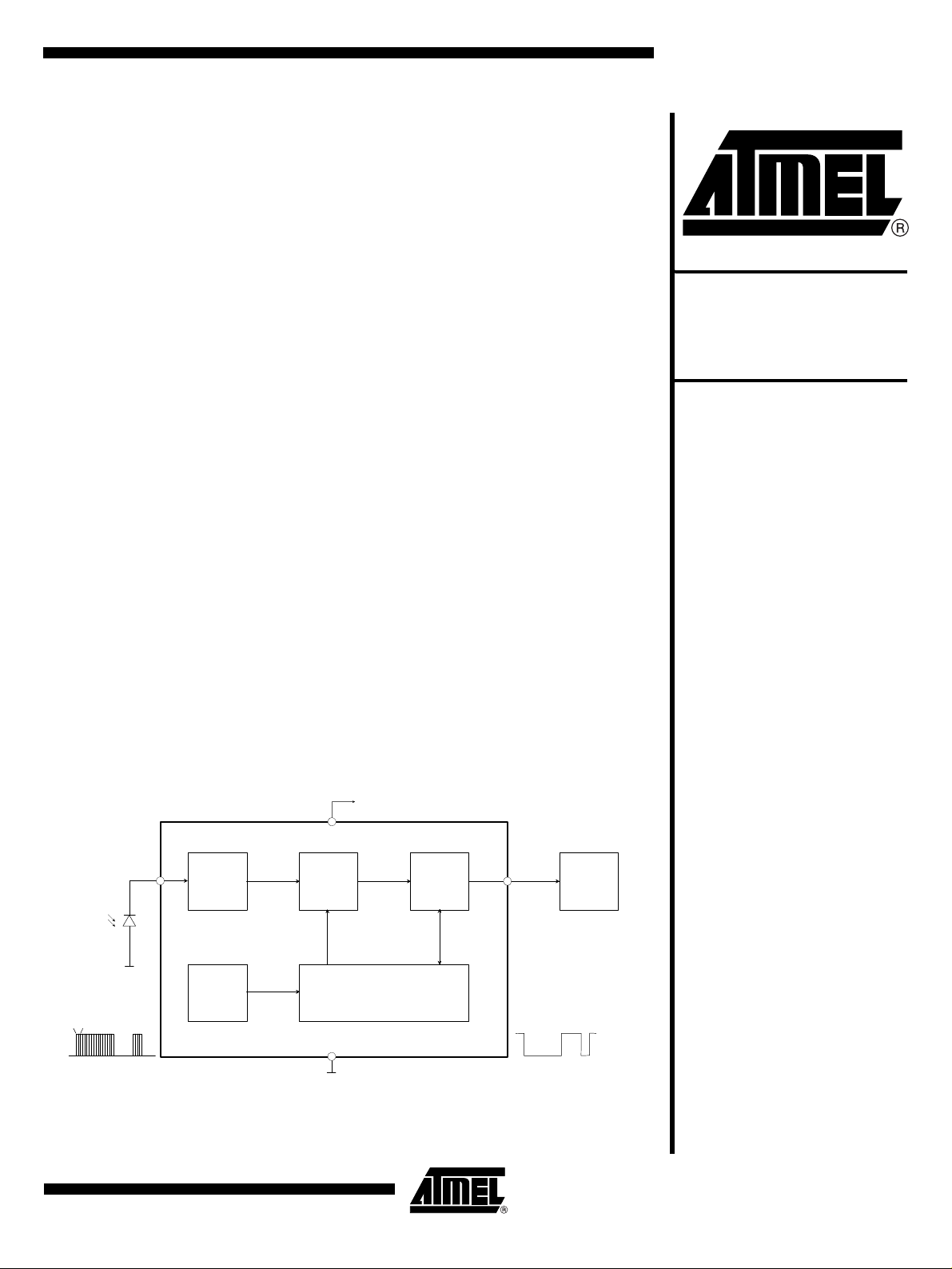
Description
The IC T2525 is a complete IR receiver for data communication developed and optimized for use in carrier-frequency-modulated transmission applications. Its function
can be described using the block diagram (see Figure 1). The input stage meets two
main functions. First, it provides a suitable bias voltage for the PIN diode. Secondly,
the pulsed photo-current signals are transformed into a voltage by a special circuit
which is optimized for low-noise applications. After amplification by a Controlled Gain
Amplifier (CGA), the signals have to pass a tuned integrated narrow bandpass filter
with a center frequency f
input signal. The demodulator is used to convert the input burst signal into a digital
envelope output pulse and to evaluate the signal information quality, i.e., unwanted
pulses will be suppressed at the output pin. All this is done by means of an integrated
dynamic feedback circuit which varies the gain as a function of the present environmental condition (ambient light, modulated lamps etc.). Other special features are
used to adapt to the current application to secure best transmission quality. The
T2525 operates in a supply-voltage range of 4.5 V to 5.5 V.
which is equivalent to the chosen carrier frequency of the
0
IR Receiver
ASSP
T2525
Figure 1. Block Diagram
Carrier frequency f
Modulated IR signal
min 6/10 pulses
IN
0
Input
Oscillator
CGA and
filter
AGC/ATC and digital
GND
VS
control
Demodulator
OUT
Micro-
controller
Rev. 4657D–AUTO–11/03
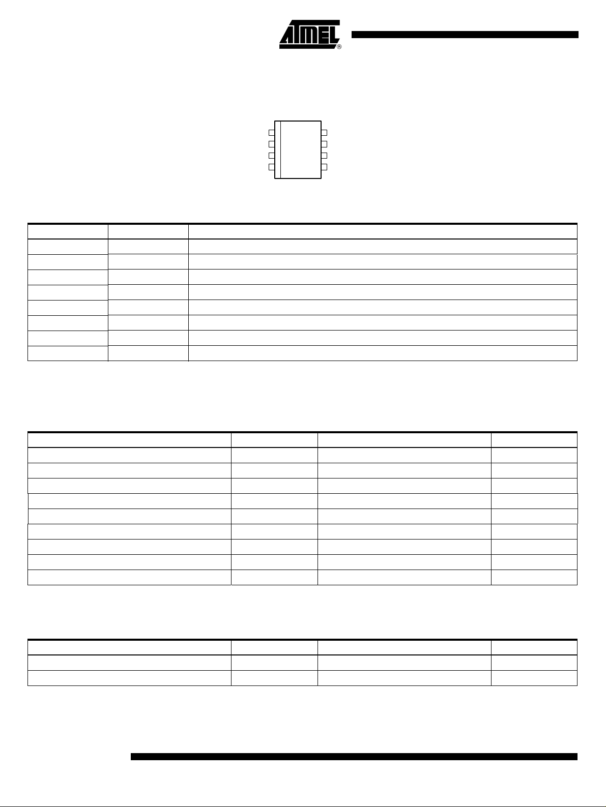
Pin Configuration
Figure 2. Pinning SO8 and TSSOP8
Pin Description
Pin Symbol Function
1 VS Supply voltage
2 NC Not connected
3 OUT Data output
4 NC Not connected
5 IN Input PIN diode
6 GND Ground
7 NC Not connected
8 NC Not connected
VS
NC
OUT
NC
1
8
NC
2
7
NC
3
6
GND
4
5
IN
Absolute Maximum Ratings
Stresses beyond those listed under “Absolute Maximum Ratings” may cause permanent damage to the device. This is a stress rating
only and functional operation of the device at these or any other conditions beyond those indicated in the operational sections of this
specification is not implied. Exposure to absolute maximum rating conditions for extended periods may affect device reliability.
Parameters Symbol Value Unit
Supply voltage V
Supply current I
Input voltage V
Input DC current at V
= 5 V I
S
Output voltage V
Output current I
Operating temperature T
Storage temperature T
Power dissipation at T
= 25°C P
amb
S
S
IN
IN
O
O
amb
stg
tot
-0.3 to +6 V
3mA
-0.3 to V
S
V
0.75 mA
-0.3 to V
S
V
10 mA
-25 to +85 °C
-40 to +125 °C
30
mW
Thermal Resistance
Parameter Symbol Value Unit
Junction ambient SO8 R
Junction ambient TSSOP8 R
thJA
thJA
130 K/W
TBD K/W
2
T2525
4657D–AUTO–11/03
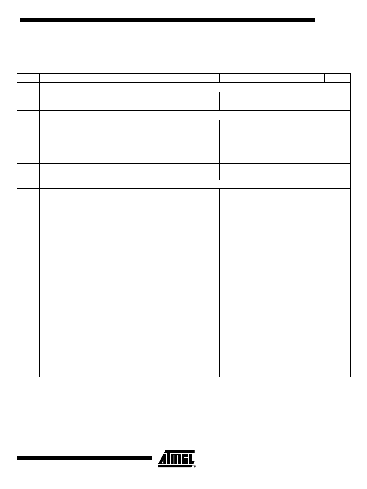
T2525
Electrical Characteristics
T
= 25°C, VS = 5 V unless otherwise specified.
amb
No. Parameters Test Conditions Pin Symbol Min. Typ. Max. Unit Type*
1 Supply
1.1 Supply-voltage range 1 V
1.2 Supply current I
= 0 1 I
IN
S
S
2Output
T
Internal pull-up
2.1
resistor
(1)
2.2 Output voltage low
2.3 Output voltage high 3,1 V
Output current
2.4
clamping
= 25°C;
amb
see Figure 9 on page 7
= 2 mA;
I
L
see Figure 9 on page 7
= 0;
R
2
see Figure 9 on page 7
1,3 R
3,6 V
3,6 I
PU
OL
OH
OCL
3 Input
3.1 Input DC current
Input DC current;
3.2
Figure 4 on page 5
IN
see Figure 9 on page 7
= 0; Vs = 5 V,
V
IN
T
= 25°C
amb
5I
5I
IN_DCMAX
IN_DCMAX
= 0;
V
Test signal:
see Figure 8 on page 7
VS = 5 V,
T
= 25°C,
Minimum detection
3.3
threshold current;
Figure 3 on page 5
amb
= 1 µA;
I
IN_DC
square pp,
burst N = 16,
f = f
; t
= 10 ms,
0
PER
3 I
Eemin
Figure 8 on page 7;
BER = 50
(2)
Test signal:
see Figure 8 on page 7
= 5 V,
V
Minimum detection
threshold current with
3.4
AC current disturbance
IIN_AC100 = 3 µA at
100 Hz
S
T
= 25°C,
amb
I
= 1 µA,
IN_DC
square pp,
burst N = 16,
f = f
; t
= 10 ms,
0
PER
3 I
Eemin
Figure 8 on page 7;
BER = 50%
(2)
*) Type means: A =100% tested, B = 100% correlation tested, C = Characterized on samples, D = Design parameter
Notes: 1. Depending on version, see “Ordering Information”
2. BER = Bit Error Rate; e.g., BER = 5% means that with P = 20 at the input pin 19...21 pulses can appear at the pin OUT
3. After transformation of input current into voltage
4.555.5V C
0.8 1.1 1.4 mA B
30/40 kW A
250 mV B
VS - 0.25 Vs V B
8mAB
-85 µA C
-530 -960 µA B
-520 pA B
-800 pA C
4657D–AUTO–11/03
3

Electrical Characteristics (Continued)
T
= 25°C, VS = 5 V unless otherwise specified.
amb
No. Parameters Test Conditions Pin Symbol Min. Typ. Max. Unit Type*
Test signal:
see Figure 8 on page 7
V
= 5 V, T
S
Maximum detection
3.5
threshold current with
> 0V
V
IN
= 1 µA;
I
IN_DC
square pp,
burst N = 16,
f = f
; t
0
Figure 8 on page 7;
BER = 5%
4 Controlled Amplifier and Filter
Maximum value of
4.1
variable gain (CGA)
Minimum value of
4.2
variable gain (CGA)
Total internal
4.3
amplification
Center frequency fusing
4.4
accuracy of bandpass
Overall accuracy center
4.5
f r e q u e n c y o f b a n d p a s s
BPF bandwidth:
type N0 - N3
4.6
BPF bandwidth:
type N6, N7
(3)
= 5 V, T
V
S
-3 dB; f
Figure 6 on page 6
-3 dB; f
Figure 6 on page 6
*) Type means: A =100% tested, B = 100% correlation tested, C = Characterized on samples, D = Design parameter
Notes: 1. Depending on version, see “Ordering Information”
2. BER = Bit Error Rate; e.g., BER = 5% means that with P = 20 at the input pin 19...21 pulses can appear at the pin OUT
3. After transformation of input current into voltage
= 25°C,
amb
= 10 ms,
PER
(2)
= 25°C f
amb
= 38 kHz; see
0
= 38 kHz
0
3I
Eemax
G
VAR MA X
G
VAR MIN
G
0_FUSE
MAX
f
0
B3.5kHzC
B5.4kHzC
-400 µA D
51 dB D
-5 dB D
71 dB D
-3 f
-6.7 f
0
0
+3 % A
+4.1 % C
ESD All pins Þ 2000V HBM; 200V MM, MIL-STD-883C, Method 3015.7
Reliability Electrical qualification (1000h) in molded SO8 plastic package
4
T2525
4657D–AUTO–11/03

T2525
Typical Electrical Curves at T
Figure 3. I
Figure 4. VIN versus I
amb
Eemin
= 25°C
versus I
IN_DC
, VS = 5 V
IN_DC
, VS = 5 V
4657D–AUTO–11/03
Figure 5. Data Transmission Rate, VS = 5 V
5

Figure 7. Illustration of Used Terms
Figure 6. Typical Bandpass Curve
Q = f0/Df; Df = -3 dB values. Example: Q = 1/(1.047 - 0.954) = 11
IN
OUT
OUT
1066 µs
533 µs
7
116
t
DON
Data word
17 ms
Burst (N=16 pulses)
t
DOFF
Envelope 1 Envelope 16
Telegram pause
T
= 62 ms
REP
Example: f = 30 kHz, burst with 16 pulses, 16 periods
Period (P=16)
7
33 µs
17056 µs/data word
7
533 µs
Data word
t
6
T2525
4657D–AUTO–11/03

Figure 8. Test Circuit
IEe = D
T2525
U1/400K
I
Ee
~
I
IN_AC100
Figure 9. Application Circuit
V
1 nF
PULSE
VS
T2525
GND
VDD = 5 V
OUT
R1 = 220
C
1
4.7 µF
DU1
20k
20k
I
IN_DC
I
IN
IN
DU2
I
= DU2/40k
IN_DC
-
DC
+
400k
1 nF
f
0
t
PER
16
= 10 ms
VDD= 5 V
I
IN_DC
(1) optional
(1)
R2
R1 = 220
I
S
RPU
> 2.4k
VS
I
IN
T2525
I
IN
OUT
OCL
I
L
Microcontroller
GND
V
IN
I
Ee
= 4.7 µF
C
1
V
O
(1)
C
= 470 pF
2
4657D–AUTO–11/03
7

Chip Dimensions Figure 10. Chip Size in µm
1130,1030
GND IN
351,904
VS
0,0
63,660
63,70
T2525
FUSING
OUT
width
h
t
g
n
e
l
723,885
Note: Pad coordinates are for lower left corner of the pad in µm from the origin 0,0
scribe
Dimensions Length inclusive scribe 1.15 mm
Width inclusive scribe 1.29 mm
Thickness 290 µ ± 5%
Pads 90 µ ´ 90 µ
Fusing pads 70 µ ´ 70 µ
Pad metallurgy Material AlCu/AlSiTi
(1)
Thickness 0.8 µm
Finish Material Si3N4/SiO
2
Thickness 0.7/0.3 µm
Note: 1. Value depends on manufacture location.
8
T2525
4657D–AUTO–11/03

Ordering Information
T2525
Extended Type
Number PL
(1)
T2525N0xx
T2525N1xx
T2525N2xx
T2525N3xx
T2525N6xx
T2525N7xx
(5)
-yyy
(1)
-DDW 1 30 2090 Standard type: ³ 10 pulses, enhanced sensibility, high data rate
(1)
(5)
-yyy
(1)
-DDW 1 40 1373
(1)
(5)
-yyy
(1)
-DDW 1 30 3415 Short burst type: ³ 6 pulses, enhanced data rate
(2)
(3)
R
PU
(4)
D
Type
2 30 2090 Standard type: ³ 10 pulses, enhanced sensibility, high data rate
2 40 1373
Lamp type: ³ 10 pulses, enhanced suppression of disturbances, secure
data transmission
Lamp type: ³ 10 pulses, enhanced suppression of disturbances, secure
data transmission
2 30 3415 Short burst type: ³ 6 pulses, enhanced data rate
Notes: 1. xx means the used carrier frequency value f0 30,33,36,38,40,44 ,56 kHz.(76 kHz type on request)
2. Two pad layout versions (see Figure 11 and Figure 12) available for different assembly demand
3. Integrated pull-up resistor at pin OUT (see “Electrical Characteristics”)
4. Typical data transmission rate up to bit/s with f0 = 56 kHz, VS = 5 V (see Figure 5 on page 5)
5. yyy means kind of packaging:
.................... .......DDW -> unsawn wafers in box
.................... .......6AQ -> (only on request, TSSOP8 taped and reeled)
Pad Layout Figure 11. Pad Layout 1 (DDW only)
GND
IN
OUT
T2525
VS
FUSING
Figure 12. Pad Layout 2 (DDW, SO8 or TSSOP8)
(6) (5)
(1)
VS
(3)
OUT
GND IN
T2525
FUSING
4657D–AUTO–11/03
9

Atmel Corporation Atmel Operations
2325 Orchard Parkway
San Jose, CA 95131, USA
Tel: 1(408) 441-0311
Fax: 1(408) 487-2600
Regional Headquarters
Europe
Atmel Sarl
Route des Arsenaux 41
Case Postale 80
CH-1705 Fribourg
Switzerland
Tel: (41) 26-426-5555
Fax: (41) 26-426-5500
Asia
Room 1219
Chinachem Golden Plaza
77 Mody Road Tsimshatsui
East Kowloon
Hong Kong
Tel: (852) 2721-9778
Fax: (852) 2722-1369
Japan
9F, Tonetsu Shinkawa Bldg.
1-24-8 Shinkawa
Chuo-ku, Tokyo 104-0033
Japan
Tel: (81) 3-3523-3551
Fax: (81) 3-3523-7581
Memory
2325 Orchard Parkway
San Jose, CA 95131, USA
Tel: 1(408) 441-0311
Fax: 1(408) 436-4314
Microcontrollers
2325 Orchard Parkway
San Jose, CA 95131, USA
Tel: 1(408) 441-0311
Fax: 1(408) 436-4314
La Chantrerie
BP 70602
44306 Nantes Cedex 3, France
Tel: (33) 2-40-18-18-18
Fax: (33) 2-40-18-19-60
ASIC/ASSP/Smart Cards
Zone Industrielle
13106 Rousset Cedex, France
Tel: (33) 4-42-53-60-00
Fax: (33) 4-42-53-60-01
1150 East Cheyenne Mtn. Blvd.
Colorado Springs, CO 80906, USA
Tel: 1(719) 576-3300
Fax: 1(719) 540-1759
Scottish Enterprise Technology Park
Maxwell Building
East Kilbride G75 0QR, Scotland
Tel: (44) 1355-803-000
Fax: (44) 1355-242-743
RF/Automotive
Theresienstrasse 2
Postfach 3535
74025 Heilbronn, Germany
Tel: (49) 71-31-67-0
Fax: (49) 71-31-67-2340
1150 East Cheyenne Mtn. Blvd.
Colorado Springs, CO 80906, USA
Tel: 1(719) 576-3300
Fax: 1(719) 540-1759
Biometrics/Imaging/Hi-Rel MPU/
High Speed Converters/RF Datacom
Avenue de Rochepleine
BP 123
38521 Saint-Egreve Cedex, France
Tel: (33) 4-76-58-30-00
Fax: (33) 4-76-58-34-80
Literature Requests
www.atmel.com/literature
Disclaimer: Atmel Corporation makes no warranty for the use of its products, other than those expressly contained in the Company’s standard
warranty which is detailed in Atmel’s Terms and Conditions located on the Company’s web site. The Company assumes no responsibility for any
errors which may appear in this document, reserves the right to change devices or specifications detailed herein at any time without notice, and
does not make any commitment to update the information contained herein. No licenses to patents or other intellectual property of Atmel are
granted by the Company in connection with the sale of Atmel products, expressly or by implication. Atmel’s products are not authorized for use
as critical components in life support devices or systems.
© Atmel Corporation 2003. All rights reserved.
®
and combinations thereof are the registered trademarks of Atmel Corporation or its subsidiaries.
Atmel
Other terms and product names may be the trademarks of others.
Printed on recycled paper.
4657D–AUTO–11/03
 Loading...