

Page 1

STK594
..............................................................................................
User Guide
Page 2

Page 3

Table of Contents
Section 1
Introduction ...........................................................................................1-1
1.1 Features....................................................................................................1-2
Section 2
Using the STK594 Top Module.............................................................2-1
2.1 Preparing the STK500 for Use with the STK594.......................................2-1
2.1.1 Adjusting VTARGET for the AT94K Devices......................................2-1
2.1.2 Connecting the STK594 to the STK500 Starter Kit ............................2-1
2.2 PORT Connectors.....................................................................................2-2
2.2.1 PORT E ..............................................................................................2-2
2.3 Programming the AT94K Devices.............................................................2-3
2.4 JTAG Connector .......................................................................................2-3
2.5 TOSC Switch.............................................................................................2-4
2.6 Universal Asynchronous Receiver Transmitter (UART)............................2-4
2.6.1 Second RS-232C Port ........................................................................2-4
2.7 Two-Wire Serial Interface (TWSI) .............................................................2-5
2.7.1 Description of Configuration Memory Pins .........................................2-5
2.8 External Interrupts.....................................................................................2-5
2.9 Split Power Supply Support ......................................................................2-6
2.10 XTAL Switch .............................................................................................2-6
2.11 Reset Switches .........................................................................................2-6
Section 3
Installing System Designer ...................................................................3-1
3.1 System Requirements...............................................................................3-1
3.2 System Designer Installation.....................................................................3-2
3.3 Configuration Programming System (CPS) Installation ............................3-2
3.4 System Designer Licensing.......................................................................3-2
3.4.1 Requesting a System Designer License.............................................3-2
3.4.2 Configuring the System Designer License .........................................3-3
3.4.3 Testing the System Designer License ................................................3-3
3.4.4 Troubleshooting..................................................................................3-3
Page 4

Section 4
Using System Designer ........................................................................4-1
4.1 Preparing the Example Files .....................................................................4-1
4.2 Description ................................................................................................4-1
4.3 Design Flow ..............................................................................................4-2
4.4 Creating a Project .....................................................................................4-2
4.5 Assembling the Microcontroller Source Code...........................................4-7
4.6 Synthesizing the FPGA Source File..........................................................4-7
4.7 AVR-FPGA Interface.................................................................................4-8
4.8 FPGA Place and Route.............................................................................4-9
4.9 Bitstream Generation ..............................................................................4-11
4.10 Programming and Design Execution ......................................................4-12
4.10.1 Hardware Setup................................................................................4-12
4.10.2 Software Setup.................................................................................4-13
4.11 Running the Design ................................................................................4-14
Section 5
Technical Specifications .......................................................................5-1
Section 6
Complete Schematics...........................................................................6-1
Page 5
Section 1
Introduction
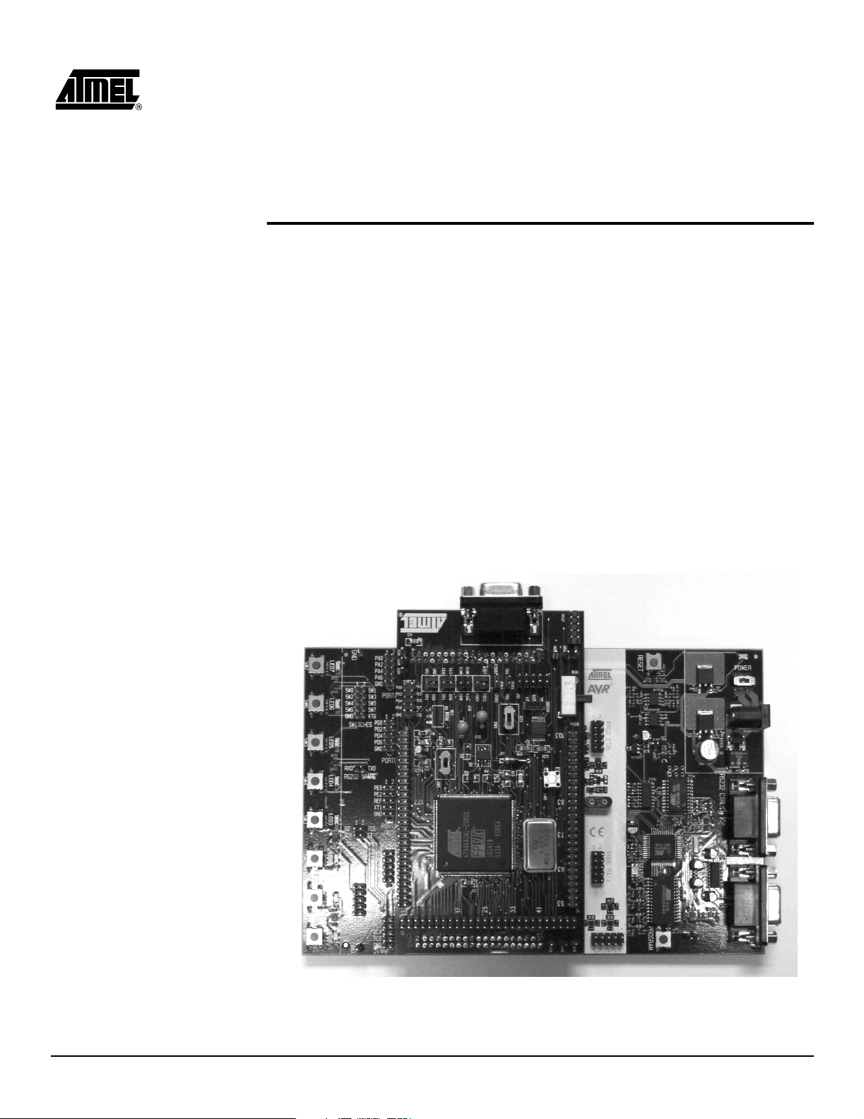
The STK594 board is a top module designed to add AT94K FPSLIC™support to the
STK500 development board. With this board the STK500 is extended to support all current AT94K FPSLIC devices in a single development environment.
The STK594 includes connectors, jumpers and hardware allowing full utilization of the
new features of the FPSLIC family, see Figure 1-1.
This user guide acts as a general getting started guide as well as a complete technical
reference for advanced users.
In addition to adding support for new devices, it also adds new support for peripherals
previously not supported by the STK500. An additional RS-232 port and a Two-Wire
Serial Interface are among the new features.
Figure 1-1.
STK594 Top Module for STK500
FPSLIC STK594 User Guide 1-1
Rev. 2819A–FPSLI–07/02
Page 6

Introduction
1.1 Features
n
STK500 Compatible
n
AVR Studio®and System Designer™Compatible
n
Supports AT94KAL and AT94KAX Devices
n
Supports all Added Features in FPSLIC Devices
n
JTAG Connector for On-chip Debugging Using JTAG ICE
n
Additional RS-232C Port with Available RTS/CTS Handshake Lines
n
On-board 32 kHz Crystal for Easy RTC Implementations
1-2 FPSLIC STK594 User Guide
2819A–FPSLI–07/02
Page 7

Section 2
Using the STK594 Top Module
2.1 Preparing the STK500 for Use with the STK594
2.1.1 Adjusting VTARGET for the AT94K Devices
2.1.2 Connecting the STK594 to the STK500 Starter Kit
Prior to using the STK594 with the STK500, it is necessary to make a few adjustments
to the STK500 Starter Kit to allow for proper operation of Atmel’s AT94K FPSLIC
devices.
According to the AT94K Series datasheet, the V
{V
|3.0<VCC= 3.6} Volts, with respect to ground. The STK594 board requires that
CC
theSTK500boardsuppliesaV
Prior to using the STK594 board, it is necessary to adjust the VTARGET to a value
between 3.0 and 3.6V. For more information on adjusting VTARGET from within AVR
Studio, consult section 5.3.5.1 of the STK500 User Guide, available on the Atmel web
site (www.atmel.com).
Note:
The STK594 should be connected to the STK500 expansion header 0 and 1. It is important that the top module is connected in the correct orientation as shown in Figure 2-1
on page 2. The EXPAND0 written on the STK594 top module should match the
EXPAND0 written beside the expansion header on the STK500 board.
It may be necessary to adjust the VDDvoltage, see “Split Power Supply Support”
on page 6 of this section for more information.
within the operating range for the AT94K devices.
CC
operating voltage is specified where
CC
FPSLIC STK594 User Guide 2-1
Rev. 2819A–FPSLI–07/02
Page 8
Using the STK594 Top Module
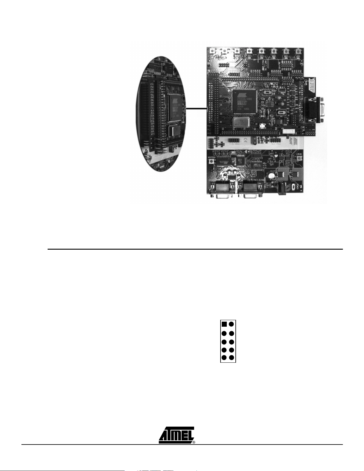
Figure 2-1.
Connecting the STK594 to the STK500 Board
Note:
Note:
2.2 PORT Connectors
2.2.1 PORT E Figure 2-2 shows the pinout for the I/O port headers Port E.
Since the AT94K devices have additional ports not available on the STK500, these ports
are located on the STK594 board. The STK594 ports have the same pinout and functionality as the ports on the STK500 board. Since Port A to Port D are already present
on the STK500 board, they are not duplicated on the STK594.
Figure 2-2.
Connecting the STK594 with the wrong orientation may damage the boards.
Do not mount the STK594 at the same time an AVR is mounted on the STK500
board.
General I/O Ports
1 2
PE0
PE2
PE4
PE6
GND
PE1
PE3
PE5
PE7
VTG
PORT E
Note:
Port E is also present on the STK500, but only PE0 to PE2 (3 least significant
bits) are accessible. To access all Port E bits the connector on the STK594
must be used.
2-2 FPSLIC STK594 User Guide
2819A–FPSLI–07/02
Page 9

Using the STK594 Top Module
2.3 Programming the AT94K Devices
The FPSLIC configuration process involves configuring the FPGA, the AVR®program
code and the FPSLIC data memory. This configuration requires a single bitstream that
configures the FPGA, the embedded AVR Program SRAM and the FPSLIC Data
SRAM. The combined bitstream is automatically generated by the Bitstream Generator,
a System Designer software utility.
After a reset and the internal clearing of the configuration data, the FPSLIC device selfinitiates configuration. The Master mode uses an internal oscillator to provide the Configuration Clock (CCLK) for clocking the external EEPROM (configurator), which
contains the configuration data. After auto-configuration is complete, re-configuration
can be initiated manually by the user, if needed.
Note:
Note:
For more details on programming procedures, refer to Section 4.10.
The AT94K devices also support Self-Programming. For more information on
this topic, refer to the “Code-Self Modify” application note available on the Atmel
web site.
The AT94K devices also support Cache Logic®Configuration. For more information on this topic, refer to the “Cache Logic Configuration” application note
available on the Atmel web site.
2.4 JTAG Connector The JTAG connector is intended for the AT94K devices that have a built-in JTAG inter-
face. The pinout of the JTAG connector is shown in Figure 2-3 and is compliant with the
pinout of the JTAG ICE available from Atmel. Connecting a JTAG ICE to this connector
allows On-chip Debugging of the AT94K devices.
More information about the JTAG ICE and On-chip Debugging can be found in the AVR
JTAG ICE user guide, available on the Atmel web site.
Figure 2-3.
JTAG Connector
1 2
TCK
TDO
TMS
VTG
TDI
GND
VTG
RST
N/C
GND
JTAG
Note:
Figure 2-4 shows how to connect the JTAG ICE probe on the STK594 board.
Figure 2-4.
To determine if your AT94K device supports JTAG Debug, examine the date
code. Any parts with a J after their date code support JTAG. Example, 4201J.
Connecting JTAG ICE to the STK594
FPSLIC STK594 User Guide 2-3
2819A–FPSLI–07/02
Page 10
Using the STK594 Top Module
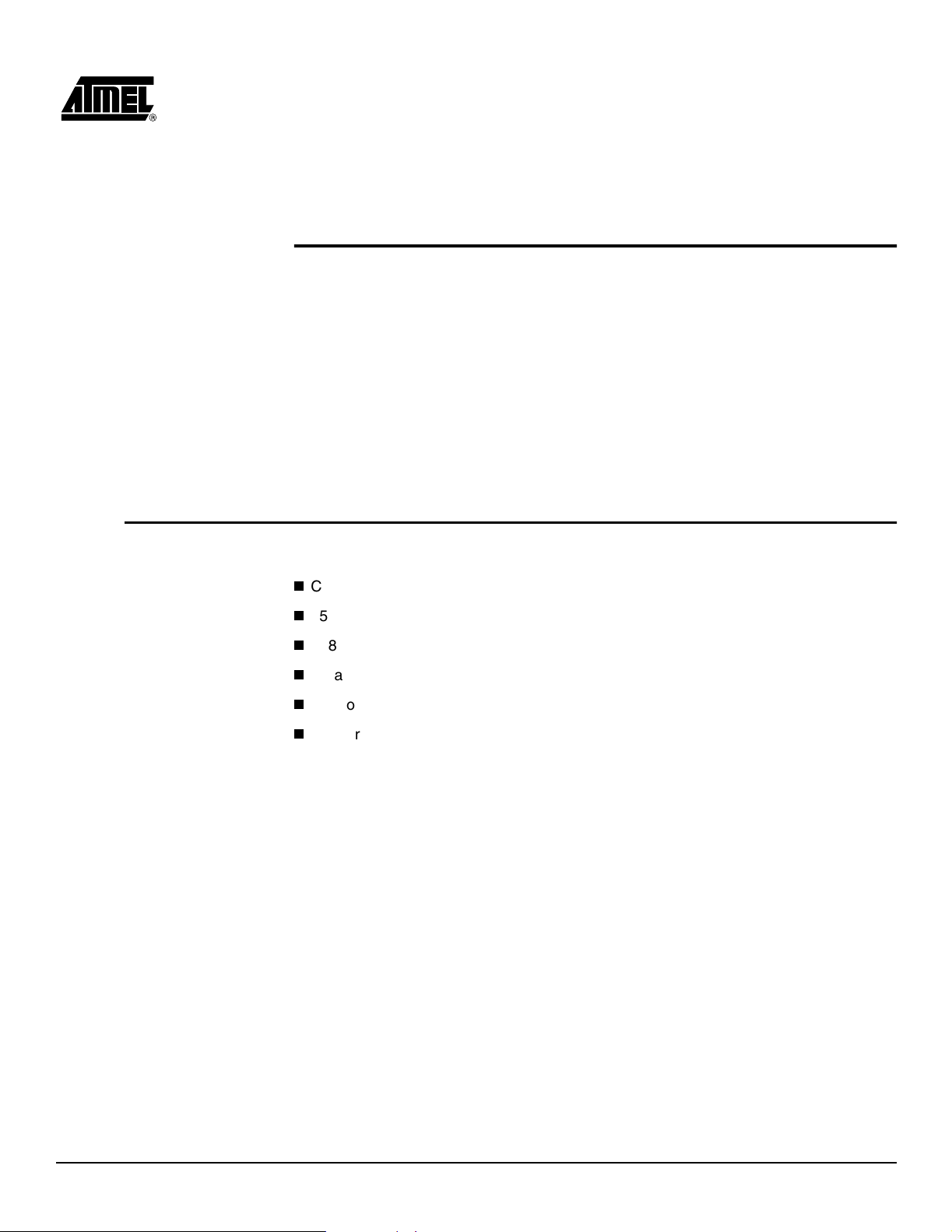
2.5 TOSC Switch The AT94K device provides dedicated I/O pins for TOSC1 and TOSC2, rather than
sharing with the general purpose I/O pins. The TOSC switch selects whether or not the
32 kHz crystal is connected to the pins of the device.
Figure 2-5 shows a simplified block schematic on how this is implemented.
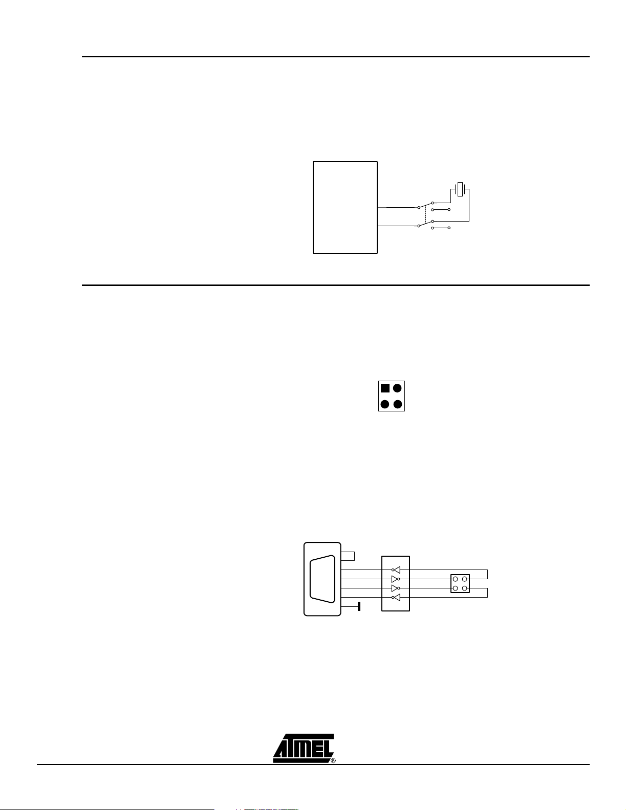
2.6 Universal Asynchronous Receiver Transmitter (UART)
Figure 2-5.
TOSC Block Schematic
FPSLIC
32 kHz
TOSC2
TOSC1
TOSC Switch
Unlike traditional AVR microcontrollers, the AT94K device provides the option of having
separate I/O pins for the UARTs rather than sharing with the general purpose I/O pins.
Figure 2-6 shows the pinout of a header for the dedicated UART pins.
Figure 2-6.
UART Header
1 2
RX0
RX1
TX0
TX1
UART
2.6.1 Second RS-232C Port
The AT94K device has an additional UART. The RS-232 port on the STK594 board has
in addition to the RXD and TXD lines support for RTS and CTS flow control. Figure 2-7
shows a simplified block schematic on how this is implemented.
Note:
The UART in AT94K devices does not support hardware RTS or CTS control. If
such functionality is needed, it must be implemented in software.
Figure 2-7.
UART Block Schematic
4
6
2
3
7
RS232 SPARE2
8
5
RS-232/Logic Level
Converter
RxD TxD
CTS RTS
This UART can also be used from devices placed in the STK500 board. Simply connect
the appropriate port pins to RXD and TXD on the STK594 board.
Note:
If no software RTS/CTS flow control is implemented, a jumper shorting RTS and
CTS will ensure correct communication with an external application that uses
such flow control.
2-4 FPSLIC STK594 User Guide
2819A–FPSLI–07/02
Page 11
Using the STK594 Top Module
2.7 Two-Wire Serial Interface (TWSI)
2.7.1 Description of Configuration Memory Pins
The AT94K device includes dedicated I/O pins for the TWSI rather than sharing with the
general purpose I/O pins.
Figure 2-8 shows the pinout of a header for the dedicated TWSI pins.
Figure 2-8.
TWSI Header
1 2
SCLSDA
TWSI
An AT17LV010-10CC 1-Mbit Configuration Memory is included on the STK594 for supplying the AT94K FPSLIC device with its configuration data, as well as for non-volatile
data storage. The configurator is a high-density EEPROM with a TWSI interface. A
detailed datasheet of the Configuration Memory can be obtained from the Atmel web
site.
The configurator can be connected to the I/O pins of the embedded AVR microcontroller. The 4-pin header marked
the configurator to the I/O pins of the target AVR microcontroller. Two-wire cables are
included with the STK500 for connecting the configurator to the I/O pins.
Figure 2-9 shows the pinout of a header for the Configuration Memory pins.
Figure 2-9.
Configuration Memory Header
CONFIG
can be used for connecting the TWSI interface of
2.8 External Interrupts
1 2
cSDA
cSER_EN
cSCL
N/C
CONFIG
Unlike traditional AVR microcontrollers, the AT94K device provides the option of having
separate I/O pins for the External Interrupts rather than sharing with the general purpose
I/O pins.
Figure 2-10 shows the pinout of a header for the dedicated External Interrupt pins.
Figure 2-10.
External Interrupt Header
1 2
INTP0
INTP2
INTP1
INTP3
EXT
FPSLIC STK594 User Guide 2-5
2819A–FPSLI–07/02
Page 12
Using the STK594 Top Module
2.9 Split Power Supply Support
The AT94K FPSLIC devices exist in two different variations, the AL and AX. The AL
variation is a 3.3V device manufactured on a 0.35µ process, while the AX variation has
a 1.8V core manufactured on a 0.18µ process. The primary difference between the two
variations, is that the AX device requires a split power supply, as the I/Os are still powered from a 3.3V supply, while the core operates at 1.8V.
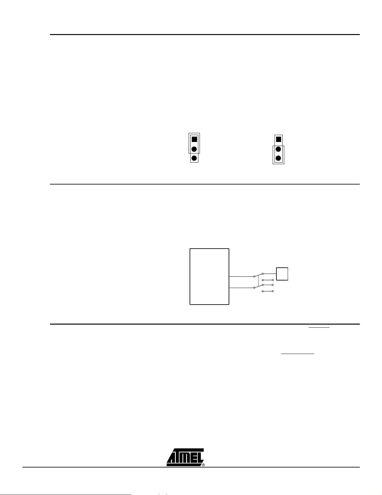
The STK594 supports both AT94K variations. If an AX variant is being used it is necessary to supply the proper core to the AT94K device. Figure 2-11 shows how to set the
jumper to select the core voltage.
Figure 2-11.
AT94K Core Voltage Selector
AT94KAL
AL
VDD
AX
AT94KAX
AL
VDD
AX
2.10 XTAL Switch An oscillator is included on the STK594 for supplying an additional clock to the AT94K
FPSLIC device. The XTAL switch selects if the oscillator is connected to the XTAL1 pin,
or whether the clock is provided by the STK500.
Figure 2-12 shows a simplified block schematic on how this is implemented.
Figure 2-12.
XTAL Block Schematic
FPSLIC
XTAL1
XTAL2
XT1
XT2
OSC
2.11 Reset Switches The reset switch found on the STK594 is connected to the AT94K’s RESET pin. When
pressed, the AT94K device will reset and initiate a configuration download from the configuration memory.
The reset switch found on the STK500 is connected to the AVRRESET
the embedded AVR microcontroller resets and begins execution at location $0000.
. When pressed,
2-6 FPSLIC STK594 User Guide
2819A–FPSLI–07/02
Page 13
Section 3
Installing System Designer
System Designer is the ideal software platform for all AT94K FPSLIC development. It
includes an Editor, an Assembler and a Debugger as its development tools for the
embedded AVR development, and also includes a Simulator, Synthesizer and a Place
and Route tool for FPGA development. System Designer also includes a Co-Verification
suite powered by Mentor Graphics
and AVR design concurrently.
®
, allowing for step-by-step simulation of the FPGA
3.1 System Requirements
For a single-user system, System Designer requires a personal computer equipped as
follows:
n
CD-ROM Drive
n
250-Mbyte Minimum Hard Drive
n
128-Mbyte RAM
n
Parallel Interface Port
n
Windows®95/98/2000/Me, or WindowsNT®4.0
n
Network Interface Card or Security Dongle
The software security dongle is used to generate a unique HOSTID for systems without
a network interface card. The security dongle is connected to the PC through the
parallel port interface. It is possible to configure a floating network license through the
security dongle. The security dongle allows users to use the software dongle on different
machines by removing and placing the dongle on other machines.
FPSLIC STK594 User Guide 3-1
Rev. 2819A–FP SLI– 07/02
Page 14

Installing System Designer
3.2 System Designer Installation
3.3 Configuration Programming System (CPS) Installation
This installation assumes that you have no previous version of System Designer
installed in your machine. If you have a previous version of the software installed or you
need step-by-step installation instructions, please refer to the System Designer “Installation, Licensing and Troubleshooting” tutorial available on the Atmel web site.
1. Insert the supplied System Designer CD-ROM into the computer. If the CD does
not automatically start, execute SETUP.EXE from the CD.
2. From the CD Browser, select
System Designer installation will perform a full installation, as there are no
optional components.
Note:
Note:
Note:
From the CD Browser, select
will install the CPS utility, which is used to program the AT17 and ATFS series configuration memories found on the STK594.
Note:
Do not install System Designer to a directory name that contains spaces, otherwise improper opperation will occur.
When you reach the portion of the System Designer installation prompting
about licensing, you should select one of two options, either
Select
outlined in Section 3.4.2 “Configuring the System Designer License”. Choose
Skip
“Requesting a System Designer License”.
AVR Studio version 3.2 or higher is required for STK500/STK594 support.
When installing the CPS utility, it is necessary to install the software in an
account with Administrator privileges if the operating system is WindowsNT or
Windows 2000/XP.
Custom
if you do not have a license and follow the instructions in Section 3.4.1
if you already have a valid license and follow the instructions
Install Products
Install Products
and select
and select
System Designer
.The
CustomorSkip
CPS for AT17 Devices
.
.This
3.4 System Designer Licensing
3.4.1 Requesting a System Designer License
The licensing of System Designer is for the Mentor Graphics tools. You can use System
Designer without a valid license, however you will not be able to use ModelSim
LeonardoSpectrum
The typical license is based on the hostID of your Network Interface Card (NIC). If you
prefer to use a dongle-based license, it is necessary that you purchase a Security Dongle from Atmel (Atmel Part Number: ATDH94DNG).
The instructions below describe the configuration of a NIC-based license. If you request
a dongle-based license, you will receive instructions on how to configure the license with
the dongle. If you wish to use a single license for multiple machines, it is necessary to
purchase a Security Dongle.
Prior to obtaining a license for System Designer, it is necessary to first install the System
Designer software suite. During installation, System Designer creates the file
LMUTIL.TXT, which is found in the C:\SystemDesigner\ETC directory, assuming a
default installation. The LMUTIL.TXT file contains the hostID of your NIC, and is composed of a combination of twelve alphanumeric characters.
Once you have installed System Designer, proceed to the FPSLIC section of the Atmel
web site and click on the
license request page is http://www.atmel.com/atmel/products/prod39r.htm.
Note:
The Serial Number is located on the white sticker on the underside of the
STK594 board or on the System Designer case.
™
or Co-Verification.
Request License
button, alternatively the direct link for the
®
,
3-2 FPSLIC STK594 User Guide
2819A–FPSLI–07/02
Page 15

Installing System Designer
3.4.2 Configuring the System Designer License
1. Once you have received your System Designer license from Atmel, place the file
in the C:\SystemDesigner directory.
2. Launch the Mentor Graphics License Configuration Utility from
> Atmel > Mentor Graphics Licensing > Configure Licensing
3. Follow the on-screen instructions. When it prompts you to select
Option
, choose3.
4. Define the
Product License Location
and press
name when defining the license location, for example
C:\SystemDesigner\fpslic.dat
. If you used a different path and/or file-
name, make the necessary changes.
Note:
If you are using Windows 95/98/Me it is necessary to reboot the machine prior
to running the System Designer software.
3.4.3 Testing the System Designer License
Once you have configured your license, you can test it by invoking the Mentor Graphics
programs that require a license.
1. Launch ModelSim from
Start > Programs > Atmel > ModelTech > ModelSim
ModelSim launches without any licensing errors, the ModelSim license has been
successfully installed.
2. Launch LeonardoSpectrum from
trum > Leonardo Spectrum
Start > Programs > Atmel > Leonardo Spec-
. If LeonardoSpectrum launches without any licensing
errors, then the LeonardoSpectrum license has been successfully installed.
3.4.4 Troubleshooting You can access the trouble shooting guide from
Shooting Guide.
Start > Programs
.
Configuration
Next
. Use the full path and file-
.If
Start > Programs > Atmel > Trouble
FPSLIC STK594 User Guide 3-3
2819A–FPSLI–07/02
Page 16

Installing System Designer
3-4 FPSLIC STK594 User Guide
2819A–FPSLI–07/02
Page 17

Section 4
Using System Designer
This tutorial will guide you through the required steps for designing and programming
AT94K series devices using System Designer.
4.1 Preparing the Example Files
Before starting the tutorial, a few preparations need to be performed:
1. Create a STK594 directory under C:\SystemDesigner\Designs\.
2. Download STK594.ZIP from the FPSLIC software page of the Atmel web site
and copy STK594.ZIP to C:\SystemDesigner\Designs\STK594.
3. Extract the contents of the STK594.ZIP file to
C:\SystemDesigner\Designs\STK594.The contents of the zip file are
shown in Table 4-1.
Table 4-1.
File Description
AT94KDEF.INC Atmel AVR Assembler AT94K FPSLIC Include File
COUNTER.PIN FPGA Pin Lock File
COUNTER.V Top Level FPGA Verilog
COUNTER.VHD Top Level FPGA VHDL
STK594.ASM Atmel AVR Assembler Source File
STK594.ZIP
®
Counter Source File
®
Counter Source File
4.2 Description The design in this tutorial is composed of a simple AVR microcontroller program and a
loadable counter implemented in the FPGA. When the counter reaches the terminal
value, an interrupt to the microcontroller will be generated using the counter’s carry-out
(RCO) signal. The interrupt is active Low and must be held for three clock cycles prior to
its acknowledgement by the microcontroller. During the Interrupt Service Routine (ISR)
the microcontroller increments the count of interrupt occurrences and places the incremented data on PORTD and the AVR-FPGA Data Bus, triggering the counter’sLOAD
signal. Once the counter has been loaded, counting will commence and the process will
be repeated. Figure 4-1 shows a simplified block diagram of the tutorial design.
FPSLIC STK594 User Guide 4-1
Rev. 2819A–FP SLI– 07/02
Page 18

Using System Designer
Figure 4-1.
Tutorial Design Block Diagram
FPGA
8-bit Counter
ENABLE
RESET
Q
LOAD
aWE
D[7:0]
RCO
CLOCK
IOSELA0
FIOWEA
AVR Data Bus 8-bit
INTA0
GCLK5
PORTD
AVR
IOSEL A0
Microcontroller
FPGA I/O SELECT 0
AVR Write Enable
FPGA Interrupt 0
Global Clock 5
4.3 Design Flow The design presented in this tutorial, only performs the required steps for designing and
programming an AT94K series device. For more information on the optional steps (i.e.
Simulation and Co-verification) please consult the FPSLIC application notes available
on the Atmel web site. Figure 4-2 outlines the design flow followed in this tutorial. For
more information on a specific step, consult the appropriate section within this tutorial.
4.4 Creating a Project
Figure 4-2.
Microcontroller
Assembly
HDL Synthesis
This tutorial uses the
Design Flow
New Project Wizard
AVR <> FPGA
Interface
FPGA
Place & Route
Bitstream
Generation
to assist with the creation of the project. The
New Project Wizard allows you to choose your Project Directory, Target Device, and
desired Tool Flow.
1. Launch System Designer from the desktop icon, or by pointing to
grams > Atmel > SystemDesigner
2. Create a new project by selecting
the
New Project Wizard
button. The
.
New
from the
Project
New Project Wizard
menu and then pressing
window opens, see Fig-
Start > Pro-
ure 4-3.
4-2 FPSLIC STK594 User Guide
2819A–FPSLI–07/02
Page 19

Using System Designer
Figure 4-3.
3. Press
New Project Wizard Window - Step 1 of 6
Next
. The window to create a project file opens, see Figure 4-4.
Figure 4-4.
New Project Wizard Window - Step 2 of 6
4. Set the Project Directory to C:\SystemDesigner\Designs\STK594, name
the project TUTORIAL and press
Next
. The part selection window appears, see
Figure 4-5.
FPSLIC STK594 User Guide 4-3
2819A–FPSLI–07/02
Page 20

Using System Designer
Figure 4-5.
5. Select
New Project Wizard Window - Step 3 of 6
AT94K40AL-25DQC
from the parts list as this is the part found on the
STK594 development board, and press
opens, see Figure 4-6.
Next
. The software tool flow window
Figure 4-6.
6. Select either
New Project Wizard Window - Step 4 of 6
Mentor - VHDLorMentor - Verilog
as the Tool Flow and press
The add parts window opens, see Figure 4-7. For this tutorial, the instructions
will assume
Mentor - Verilog
has been selected.
Next
.
4-4 FPSLIC STK594 User Guide
2819A–FPSLI–07/02
Page 21

Using System Designer
Figure 4-7.
7. Select
New Project Wizard Window - Step 5 of 6
Done with Parts
. System Designer supports multiple part partitioning,
however for this tutorial only one part will be used. Press
the wizard opens, see Figure 4-8.
Next
. The last step of
Figure 4-8.
8. Press
New Project Wizard Window - Step 6 of 6
Finish
to exit the
New Project Wizard
the TUTORIAL design, see Figure 4-9.
. The project window now contains
FPSLIC STK594 User Guide 4-5
2819A–FPSLI–07/02
Page 22

Using System Designer
Figure 4-9.
Project Window
9. From the System Designer desktop, click on the
switch to the
Figure 4-10.
Design Flow Manager
Design Flow Manager
, see Figure 4-10.
Part Graphic
(see Figure 4-9) to
The Design Flow Manager shows the steps available for designing with Atmel FPSLIC
devices. The red and blue arrows show the dependencies between the various stages
of development. This tutorial will only show the minimum steps in order to complete a
design. The remainder of the steps involves simulation and co-verification. For further
information on simulation and co-verification, please consult the “Quick Start Tutorial”
available on the Atmel web site.
4-6 FPSLIC STK594 User Guide
2819A–FPSLI–07/02
Page 23

Using System Designer
4.5 Assembling the Microcontroller Source Code
4.6 Synthesizing the FPGA Source File
The Atmel AVR Assembler translates assembly source code into object code. The generated object code can then be used as an input to a simulator, emulator such as the
Atmel AVR JTAG In-Circuit Emulator (ICE), or used to program the target device. The
Assembler generates fixed code allocations, therefore no linking is necessary.
1. Press the
2. Go to the
3. Browse to the C:\SystemDesigner\Designs\STK594 directory and select
STK594.ASM.
4. Press
successful.
Note:
For design entry using assembly language, consult the AT94K datasheet for a summary
of instructions supported by the FPSLIC devices. The complete “AVR Instruction Set
Nomenclature” describes each instruction in detail and has been installed as part of the
System Designer Tool. The AVR Instruction Set Nomenclature and FPSLIC datasheet
can be accessed from the Help menu and choosing
1. Synthesis translates the VHDL or Verilog source code into gate-level technologyspecific file for use with the target FPGA Place and Route tool.
2. Press the Synthesis Tool button. A dialog box to add VHDL files appears, see
Figure 4-11.
SW Compiler
File
menu and choose
Assemble
If assembly was not successful, make sure the include file AT94KDEF.INC is in
the design directory.
and close the Atmel AVR Assembler if assembly was
button to open the Atmel AVR Assembler.
Open
.
Online Resources > Resources
.
Figure 4-11.
3. Press yes. A file selection window appears.
4. Select COUNTER.V and press
5. Close the
AT94K
COUNTER.EDF under Output.
6. Press
Add VHDL Files Dialog Box
Tip of the Day
as the
Technology
Run Flow
. Figure 4-12 shows a successful synthesis.
dialog if shown. Leonardo automatically selects Atmel
and lists COUNTER.V under
OK.
LeonardoSpectrum opens.
Input
. Leonardo®also lists
FPSLIC STK594 User Guide 4-7
2819A–FPSLI–07/02
Page 24

Using System Designer
Figure 4-12.
7. Close Leonardo Spectrum, when prompted to save your project press
Leonardo Spectrum, Successful Synthesis
No.
4.7 AVR-FPGA Interface
The AVR-FPGA Interface dialog provides a means for making the connections between
the embedded FPGA and AVR microcontroller.
1. Press the
2. Select
Por ts
counter
dialog appears, see Figure 4-13.
Figure 4-13.
AVR-FP G A
and pressOKwhen prompted for Top-Level Entity. The
Select Ports Dialog
Interface button.
Select
4-8 FPSLIC STK594 User Guide
2819A–FPSLI–07/02
Page 25

Using System Designer
3. Connect the counter's
4. Select the
5. Select the
the
AVRIoSelects
6. Press
AVRIoSelects
LOAD
Connect
.
LOAD
signal to
tab on the right-hand side of the dialog box.
signal from the
.
FPGA-AVR I/O Select 0
Input Design Ports
and select
.
IOSELA0
7. Connect the remaining inputs and outputs as shown in Table 4-2.
Table 4-2.
8. Uncheck
Select Ports
FPGA-AVR Interface Connections
FPGA I/O FPGA-AVR I/O Select Ports Tab
LOAD OSELA0 AVRIoSelects
RCO INTA0 FPGAInterrupts
D(7:0) ADINA(7:0) DataFromAVR
aWE FIOWEA AVRControls
CLK GCLK5 AVRClocks
Generate Template Test Bench File
on the bottom left-hand side of the
dialog. Since we are not performing co-verification, it is not neces-
sary to generate the pre-layout test bench file.
9. Press
OK.
from
4.8 FPGA Place and Route
The Figaro Integrated Development System (IDS) is used as the FPGA Place &
Route tool. Figaro takes the gate-level technology-specific file generated by the synthesis tool and partitions, places, and routes the FPGA design.
1. Press the
Figaro IDS
buttontoopenthe
FPGA Place & Route Tools Settings
log, see Figure 4-14.
Figure 4-14.
FPGA Place & Route Tools Settings Dialog
dia-
FPSLIC STK594 User Guide 4-9
2819A–FPSLI–07/02
Page 26

Using System Designer
2. Select
Open EDIF Netlist
and Browse to select COUNTER.EDF, then pressOK.
Figaro should open and complete the
once completed the
Figure 4-15.
Figaro Batch Options Dialog
Figaro Batch Options
Open,Map
, and
Par ts
steps automatically,
dialog appears, see Figure 4-15.
The Figaro Batch Options allows for the setting of Design Constraints (i.e. Pin Locking) and Place and Route quality:
Design Constraints
a. Press
Locks
Import Constraints
GUI to perform the pin locking, but since a *.PIN file is supplied, the
.Alternatively,wecouldhaveusedthe
Assign Pin
import method will be used.
b. Select COUNTER.PIN and press
OK
.
Place and Route
a. Use the default setting for
Quality
. Quality sets the trade-off between Figaro’s
speed and the efficiency of the Place & Route result, see the online help for
further information.
b. Use the default setting for
Timing Driven Design
. Checking the Timing Driven
Design box allows Figaro to take account of critical paths when performing
the Place & Route, see the online help for further information.
c. Press
Compile
, once completed the Figaro IDS
Compile
button will turn
green.
d. Select
from the
File
menu, when prompted to save your design select
Exit
Ye s .
4-10 FPSLIC STK594 User Guide
2819A–FPSLI–07/02
Page 27

Using System Designer
4.9 Bitstream Generation
The Bitstream Generator takes the outputs from both the FPGA and AVR compilers,
and generates a single programming file for use in configuring the AT94K device.
1. Press Bitstream Generation to open the bitstream utility. The FPSLIC Control
Register Settings dialog opens, see Figure 4-16.
Figure 4-16.
FPSLIC Control Register Settings Dialog
2. Check the
Include FPGA Bitstream
box and select COUNTER.BST by pressing
Browse.
3. Check the
Browse
4. Select the Control Register Settings tab and use the default settings, see Figure
4-17.
FPSLIC STK594 User Guide 4-11
Include AVR Hex File
.
box and select STK594.HEX by pressing
2819A–FPSLI–07/02
Page 28

Using System Designer
Figure 4-17.
Control Register Settings Dialog
OK
5. Press
Note:
4.10 Programming and Design Execution
4.10.1 Hardware Setup Before programming the configurator and verifying the tutorial design, a few prepara-
The programming file generated by the Bitstream Generator is used to program the configuration memory. When the FPSLIC requests configuration data after a Reset or
Power-On-Reset, the data is clocked out serially.
tions need to be performed prior to its execution on hardware.
1. Connect the PC’s parallel port to the 25-pin connector of the ATDH2225 Programming Dongle.
2. Connect the 10-pin ISP header on the STK594 to the 10-pin ribbon cable of the
ATDH2225. The ATDH2225 is keyed to assure proper orientation, see Figure 4-
18.
to generate the combined bitstream file.
It is possible to generate a bitstream for only the FPGA or AVR as you may only
want to program that portion of the FPSLIC device. To include only the AVR
HEX file, simply uncheck the Include FPGA Bitstream box. Programming only
the FPGA portion can be done in a similar fashion.
4-12 FPSLIC STK594 User Guide
2819A–FPSLI–07/02
Page 29

Using System Designer
Figure 4-18.
3. Place the Programming switch in the
4. Using a 10-wire ribbon cable from the STK500, connect
5. Using a 2-wire cable from the STK500, connect
In-System Programming
PROG
position.
SW0
PORTD
and
to the
SW1
to FPSLIC pins
LEDS.
177 and 178, respectively.
6. Connect the Power Supply from an AC outlet to the power connector on the
STK500 development board.
7. Turn on the STK500.
Note:
Prior to providing power to the STK500 development board it is necessary to
adjust the VTARGET supplied by the STK500 to the STK594, for more information on this adjustment please refer to Section 2.1.1.
4.10.2 Software Setup The CPS utility allows for the programming, reading, and verification of data. CPS supports Atmel’s AT17F, ATFS and AT17LV series of configuration memories.
1. Press the
CPS
button, see Figure 4-19.
FPSLIC STK594 User Guide 4-13
2819A–FPSLI–07/02
Page 30

Using System Designer
Figure 4-19.
CPS
4.11 Running the
Design
2. Select
3. Select FPSLIC_COUNTER.BST under
4. Select OUT.BST under
5. Select1Munder
6. Select
7. Select
8. Select
the ATDH2225 programming adapter).
9. Select
10. Select
11. Press
CPS log window.
Note:
Once programming has completed, it is necessary to move the Programming
Switch to the RUN position for configuration of the FPSLIC device to occur. If the
LEDs on the STK500 begin to count, the configuration has occurred. If the configuration does not occur, press the
initiate a configuration download. Alternatively, power-cycling the STK500 will also
initiate a configuration download.
/P: Partition, program, and verify from an Atmel file
Input File
.
Output File.
EEPROM Density
Low
under
Reset Polarity.
AT40K/AT94K
LPT1
under
Slow
under
Low
under
Start Procedure
If the CPS utility is being launched for the first time, the clock calibration dialog
will be displayed. Press
accurate calibration. The Checksum is the number of data bits found in the BST
file, and it can be used to check if the data is corrupted during programming.
under
FPGA Family.
COMM Port
Data Rate
A2 Bit Level
. When finished a statistics report will be provided in the
.
(assuming LPT1 is the parallel port connected to
.
.
Yes
to proceed with calibration and select
RESET
button found on the STK594 board to
under
Procedure.
High
for
4-14 FPSLIC STK594 User Guide
2819A–FPSLI–07/02
Page 31

Section 5
Technical Specifications
System Unit
PhysicalDimensions..........................................5.125” x2.75”
Weight............................................................6oz.
Operating Conditions
Voltage Supply ...................................V
Connections
Serial Connector . . . ....................................9-pinD-SUBFemale
Serial Communications Speed ..................................... 250kbps
=3.3V,VDD= 1.8/3.3V
CC
FPSLIC STK594 User Guide 5-1
Rev. 2819A–FP SLI– 07/02
Page 32

Technical Specifications
5-2 FPSLIC STK594 User Guide
2819A–FPSLI–07/02
Page 33

Section 6
Complete Schematics
See the following pages the complete schematics and assembly drawings of the
STK594.
FPSLIC STK594 User Guide 6-1
Rev. 2819A–FP SLI– 07/02
Page 34

2819A–FPSLI–07/02
6-2 FPSLIC STK594 User Guide
Complete Schematics
5
D D
4
TOSC1
TOSC2
TOSC1
TOSC2
2
5
SW1
1
3
4
6
SW DPDT
3
R1
200K
2
1
R2
10M
XT1
XT2
Y1
32.768 kHz
C2
27 pF
Y2
5
OUT
OSC8
C C
C1
33 pF
B
XTAL1
XTAL2
XTAL1
XTAL2
SW2
2
5
XT1
1
3
XT2
4
6
SW DPDT
B
A A
ATSTK594 : Clock Circuitry
Title
ASize Document Number Rev A
Date: Sheet 1of 6
5
4
3
Friday, April 26, 2002
2
CHW5472
1
Page 35

Complete Schematics
Sheet 2 of 6
1
PDT[7..0]
PDT[7..0]
PET[7..0]
PET[7..0]
STK594 : AT94K FPSLICTitle
1
CHW5472
Friday, April 26, 2002
CSize Document Number Rev A
Date:
XTAL2
XTAL1
TOSC1
TOSC2
CCLK
D0
INTP3
INTP2
INTP1
RX1
155
156
NC
NC
NC
GND
I/O
I/O
I/O
CS1 (I/O)
I/O
I/O
I/O
I/O
I/O
GND
I/O
I/O
I/O
I/O
I/O
I/O
I/O
I/O
I/O
I/O
GND
VDD
I/O
I/O
I/O
I/O
I/O
I/O
I/O
I/O
I/O
I/O
GND
I/O
I/O
I/O
I/O
I/O
I/O
I/O
I/O
I/O
VCC
NC
NC
NC
NC
123
GND
123456789
J2
TX1
VCC
TOSC1
TOSC2D0CCLK
INTP3
TX1
RX1
INTP2
INTP1
145
146
147
148
149
150
151
152
153
154
D0
NC
TX1
RX1
VCC
CCLK
INTP1
INTP2
TOSC1
TOSC2
TESTCLOCK
INTP3 (CSOUT)
GCK7 (I/O)
GCK8 (I/O)
I/O
I/O
I/O
I/O
I/O
I/O
GND
NC
I/O
I/O
GCK1 (I/O)
6
7
8
9
5
4
10
11
121314151617181920212223242526272829303132333435363738394041424344454647484950
GCK1
10111213141516171819202122232425262728293031323334353637383940414243444546474849505152
2
GCK7
GCK8
52
51
50
49
48
47
46
45
44
43
42
41
40
39
38
37
36
35
34
33
32
31
30
29
28
3
27
26
25
24
23
22
21
20
19
18
17
16
15
14
13
12
11
10
9
8
7
6
5
4
3
2
1
J1
CON52
157
158
159
160
GND
161
162
GCK7
163
164
165
CS1
166
167
168
169
170
171
GND
172
173
174
175
176
177
178
179
180
181
GND
182
183
VDD
184
185
186
187
188
189
190
191
192
193
194
GND
195
196
197
198
199
200
201
202
203
204
GCK8
205
VCC
206
207
208
U1
4
INTP0
RX0
TX0
GND
XTAL2
XTAL1
TX0
RX0
INTP0
135
136
137
138
139
140
141
142
143
144
NC
NC
NC
NC
TX0
RX0
GND
INTP0
XTAL1
XTAL2
SCL
SDA
VDD
GND
SCL
SDA
PET3
PET4
PET5
PET6
PET7
PDT6
PDT5
PDT4
PDT7
130
131
132
133
134
PE6
PD7
GND
PDT3
118
119
120
121
122
123
124
125
126
127
128
129
PE4
PE5
PE3
SCL
PD5
PD6
PD3
PD4
CS0
SDA
VDD
PE7 (CHECK)
AT94K40-25DQC
I/O
GND
FCK1 (I/O)
I/O
I/O
I/O
I/O
I/O
I/O
I/O
I/O
I/O
GND
VDD
I/O
I/O
I/O
I/O
I/O
I/O
I/O
I/O
I/O
FCK2 (I/O)
GND
I/O
I/O
GND
VDD
GND
GND
RESET
TDI
TDO
TMS
TCK
INIT
CON
GCK3
GCK4
VCC
RESET
PET1
PET2
PDT2
PET0
PDT1
PDT0
105
106
107
108
109
110
111
112
113
114
115
116
117
NCNCNCNCNC
I/O
I/O
I/O
NC
NC
PE0
PE1
PE2
PD0
PD1
PD2
VCC
RESET
NC
104
CON
103
NC
102
GND
101
GCK4 (I/O)
100
I/O
99
I/O
98
I/O
97
I/O
96
I/O
95
I/O
94
I/O
93
I/O
92
I/O
91
GND
90
I/O
89
I/O
88
I/O
87
I/O
86
I/O
85
I/O
84
I/O
83
I/O
82
I/O
81
I/O
80
GND
79
VDD
78
INIT (I/O)
77
I/O
76
I/O
75
I/O
74
I/O
73
I/O
72
TCK (I/O)
71
TMS (I/O)
70
I/O
69
I/O
68
GND
67
I/O
66
I/O
65
I/O
64
I/O
63
LDC/TDO (I/O)
62
I/O
61
I/O
60
I/O
59
HDC/TDI (I/O)
58
GCK3 (I/O)
57
M2
56
VCC
55
NC
54
NC
53
NC
I/O
I/O
I/O
OTS (I/O)
GCK2 (I/O)
AVRRESET
GNDM0NC
51
52
RST
OTS
GCK2
GND
M0
52
51
CON
50
49
GND
48
GCK4
47
46
45
44
43
42
41
40
39
38
GND
37
36
35
34
33
32
31
30
29
28
27
GND
26
VDD
25
INIT
24
23
22
21
20
19
TCK
18
TMS
17
16
15
GND
14
13
12
11
10
LDC TDO
9
8
7
6
HDC TDI
5
GCK3
4
M2
3
VCC
2
1
J3
CON52
2
3
4
CON52
R3
2K7
5
52 Pi n connectors are double rows of Probe
pins, 26x2 on each side of the chip.
VCC
RST
GCK1
Add Labels to connectors
every 10 pins. Labels should match chip pin numbers
up to 208
D D
C C
GCK2
B B
C6
0.1 uF
C5
0.1 uF
C4
0.1 uF
C3
0.1 uF
VCC VCCVCC VCC
A A
C10
0.1 uF
C9
0.1 uF
5
C8
0.1 uF
C7
0.1 uF
VDD VDDVDD VDD
FPSLIC STK594 User Guide 6-3
2819A–FPSLI–07/02
Page 36

Complete Schematics
1
2
AUX_I[1..0]
AUX_O[1..0]
AUX_O[1..0]
AUX_I[1..0]
PBM2
PBM6
PBM4
AUX_O1
246
8
J5
135791113151719212325272931333537
AUX_I1
PBM3
PBM5
PBM7
DSOT
DCST
XT2
PBT6
PBT0
PBT4
PDT2
DCST
PBM0
DSOT
XT2
PDT4
PDT6
GND
VTGVTG
PBT2
101214161820222426283032343638
GND
DCKT
XT1
PBM1
PBT7
PDT7
PBT5
DSIT
DSIT
DCKT
XT1
PDT3
PDT5
PBT3
PBT1
PBT[7..0]
PBM[7..0]
SCL
PBT[7..0]
PBM[7..0]
PDT[7..0]PAT[7..0]
R4
2K7
1
VCC
CHW5472
TXD
RST
cSCL
cSCL
GND
J7
TCK GND
RST
VTG
246
13579
VTG
TDO
TCK
TDO
TMS
2
4
8
10
J8
CON10A
cSDA
cSER_EN
TDI
cSDA
cSER_EN
GND
PDT0
40
CON40A
39
GND
PDT1
RTS
Friday, April 26, 2002Date: Sheet 3 of 6
TXDRXD
RTS
2
4
J10
CON4A13
J12
CON2A
CTS
RXD
CTS
12
SDA SCL
SDA
CON4A13
STK594 : HeadersTitle
Size B Document Number Rev A
2
C13
0.1 uF
C12
0.1 uF
3
VCC VTG
PET[2..0]
PCM[7..0]
PCT[7..0]
PAT[7..0] PDT[7..0]
PCT[7..0]
PET[2..0]
PCM[7..0]
VCC VCC
VCC
C11
0.1 uF
3
PET[7..0]
4
J4
AREFT
GNDGND GNDGND
PET2
PCT4
PET0
PCM4
PCM0
PCM6
AREFT
PCM2
AUX_O0
246
8
101214161820222426283032343638
PCT0
PCT6
VTG
PCT2
PAT6
GND
PAT4
135791113151719212325272931333537
VADJ
PCM1
PCM7
AUX_I0
PCM3
PCM5
RST
VADJ
PCT5
PCT1
VTG
PCT7
PAT7
PAT5
PCT3
GND
PET1
RST
PAT0
PAT2
GND
40
CON40A
39
PAT1
GND
PAT3
PET[7..0]
PET1
VTG TDI
PET7
PET5
PET3PET2
246
8
10
J6
CON10A
13579
PET0
PET6
PET4 TMS
GND
INTP1
INTP3
INTP3
2
4
J9
CON4A
1
3
INTP0 INTP1
INTP2
INTP0
INTP2
TX0
TX1
2
J11
1
RX0 TX0
RX1
RX0
TX1
4
3
RX1
CON4A
TOSC2
TOSC2
J13
CON2A
12
TOSC1
TOSC1
4
5
D D
C C
B B
A A
5
6-4 FPSLIC STK594 User Guide
2819A–FPSLI–07/02
Page 37

FPSLIC STK594 User Guide 6-5
5
4
3
2
1
VCCVCC
D D
CCLK
cSCL
INIT
cSER_EN
CCLK
cSCL
cSER_EN
CON
C C
VCC
R7
4K7
D1
RESET
B B
RESET
1 2
C14
0.003 uF
1N4001
R5
2K7
INIT
SER_EN
CON
U2
3
RESET/OE
7
SER_EN
4
CE
AT17LV010/LAP
VCC
DATACLK
CEO
R6
2K7
D0
12
cSDA
D0
cSDA
6
J14
1
2
3
4
5
6
SW3
12
11
10
9
8
7
6
5
4
3
2
1
7
9
CON10A
VCCGND
8
10
SW 4PDT
2819A–FPSLI–07/02
SW4 C15
A A
0.1 uF
STK594 : In-System Programming CircuitryTitle
A
Size CHW5472Document Number Rev A
5
4
3
Friday, April 26, 2002Date:
2
Sheet 4 of 6
1
Complete Schematics
Page 38

2819A–FPSLI–07/02
6-6 FPSLIC STK594 User Guide
Complete Schematics
5
D D
VCC VDD VOUT
J15
VCC
1
C C
VDD
2
VOUT
3
CON3
4
VCC VOUT
C16
10 uF
3
U3
1
LT1117-1.8/SOT
VOUTVIN
ADJ/GND
2
1
23
C17
10 uF
B B
TP1
GND VCC V DD
1
T POINT F
A A
TP2
1
T POINT F
TP3
1
T POINT F
STK594 : Split Power Rail CircuitryTitle
A
Size CHW5472Document Number Rev A
5
4
3
Friday, April 26, 2002Date:
2
Sheet 5 of 6
1
Page 39

FPSLIC STK594 User Guide 6-7
5
D D
4
3
2
1
VCC
C18
0.1 uF
U4
CTS
C C
C19
0.1 uF
C20
0.1 uF
RXD
TXD
RTS
CTS
RXD
TXD
RTS
9
R2OUT
12
R1OUT
11
T1IN
10
T2IN
1
C1+
3
C1-
4
C2+
5
C2-
2
V+
6
V-
R2IN
R1IN
T1OUT
T2OUT
8
13
14
7
GND
P1
5
9
4
8
3
7
2
6
1
CONNECTOR DB9
MAX3232
B B
C21
0.1 uF
2819A–FPSLI–07/02
VCC
C22
A A
0.1 uF
STK594 : RS-232 Spare #2 CircuitryTitle
A
Size CHW5472Document Number Rev A
5
4
3
Friday, April 26, 2002Date:
2
Sheet 6 of 6
1
Complete Schematics
Page 40

Complete Schematics
6-8 FPSLIC STK594 User Guide
2819A–FPSLI–07/02
Page 41

Atmel Headquarters Atmel Operations
Corporate Headquarters
2325 Orchard Parkway
San Jose, CA 95131
TEL 1(408) 441-0311
FAX 1(408) 487-2600
Europe
Atmel Sarl
Route des Arsenaux 41
Case Postale 80
CH-1705 Fribourg
Switzerland
TEL (41) 26-426-5555
FAX (41) 26-426-5500
Asia
Room 1219
Chinachem Golden Plaza
77 Mody Road Tsimhatsui
East Kowloon
Hong Kong
TEL (852) 2721-9778
FAX (852) 2722-1369
Japan
9F, Tonetsu Shinkawa Bldg.
1-24-8 Shinkawa
Chuo-ku, Tokyo 104-0033
Japan
TEL (81) 3-3523-3551
FAX (81) 3-3523-7581
Memory
2325 Orchard Parkway
San Jose, CA 95131
TEL 1(408) 441-0311
FAX 1(408) 436-4314
Microcontrollers
2325 Orchard Parkway
San Jose, CA 95131
TEL 1(408) 441-0311
FAX 1(408) 436-4314
La Chantrerie
BP 70602
44306 Nantes Cedex 3, France
TEL (33) 2-40-18-18-18
FAX (33) 2-40-18-19-60
ASIC/ASSP/Smart Cards
Zone Industrielle
13106 Rousset Cedex, France
TEL (33) 4-42-53-60-00
FAX (33) 4-42-53-60-01
1150 East Cheyenne Mtn. Blvd.
Colorado Springs, CO 80906
TEL 1(719) 576-3300
FAX 1(719) 540-1759
Scottish Enterprise Technology Park
Maxwell Building
East Kilbride G75 0QR, Scotland
TEL (44) 1355-803-000
FAX (44) 1355-242-743
RF/Automotive
Theresienstrasse 2
Postfach 3535
74025 Heilbronn, Germany
TEL (49) 71-31-67-0
FAX (49) 71-31-67-2340
1150 East Cheyenne Mtn. Blvd.
Colorado Springs, CO 80906
TEL 1(719) 576-3300
FAX 1(719) 540-1759
Biometrics/Imaging/Hi-Rel MPU/
High Speed Converters/RF Datacom
Avenue de Rochepleine
BP 123
38521 Saint-Egreve Cedex, France
TEL (33) 4-76-58-30-00
FAX (33) 4-76-58-34-80
Atmel Programmable SLI Hotline
(408) 436-4119
Atmel Programmable SLI e-mail
fpslic@atmel.com
e-mail
literature@atmel.com
Web Site
http://www.atmel.com
FAQ
Available on web site
© Atmel Corporation 2002.
Atmel Corporation makes no warranty for the use of its products, other than those expressly contained in the Company’s standard warranty
whichisdetailedinAtmel’s Terms and Conditions located on the Company’s web site. The Company assumes no responsibility for any errors
which may appear in this document, reserves the right to change devices or specifications detailed herein at any time without notice, and does
not make any commitment to update the information contained herein. No licenses to patents or other intellectual property of Atmel are granted
by the Company in connection with the sale of Atmel products, expressly or by implication. Atmel’s products are not authorized for use as critical
components in life support devices or systems.
AT ME L®,AVR®,AVRStudio®and Cache Logic®are the registered trademarks of Atmel; FPSLIC™and System Designer
tered trademarks of Mentor Graphics Corporation; LeoanrdoSpectrum
Corporation; Verilog
registered trademark of Cadence Design Systems Inc. Microsoft
trademarks of Microsoft Corporation.
Other terms and product names may be the trademarks of others.
™
are the trademarks of Atmel. Mentor Graphics®, ModelSim®and Leoanrdo®are the regis-
®
is the registered trademark of Gateway Design Automation Corporation; VHDL®is the
™
is the trademark of Mentor Graphics
®
and Microsoft NT®are the registered
Printed on recycled paper.
2819A–FPSLI–07/02
/xM
 Loading...