

Page 1

STK525
.............................................................................................
Hardware User Guide
Page 2

Section 1
Introduction...........................................................................................1-3
1.1 Overview...................................................................................................1-3
1.2 STK525 Starter Kit Features.....................................................................1-4
Section 2
Using the STK525.................................................................................2-6
2.1 Overview...................................................................................................2-6
2.2 Power Supply............................................................................................2- 7
2.3 RESET....................................................................................................2-10
2.4 AT90USBxxx AVR Microcontroller..........................................................2-11
2.5 Serial Links .............................................................................................2-11
2.6 On-board Resources...............................................................................2-14
2.7 STK500 Resources.................................................................................2-19
2.8 In-System Programming.........................................................................2-20
2.10 Test Points..............................................................................................2-23
2.11 Configuration Pads .................................................................................2-24
2.12 Solder Pads ............................................................................................2-25
Section 3
Troubleshooting Guide.......................................................................3-26
Section 4
Technical Specifications................... ......... .......... ......... ......... .......... ...4-27
Section 5
Technical Support............................. ......... .......... ......... ......... .......... ...5-28
Section 6
Complete Schematics.......................................... ......... ......... .......... ...6-29
STK525 Hardware User Guide User Guide 1
7608A–AVR–04/06
Page 3

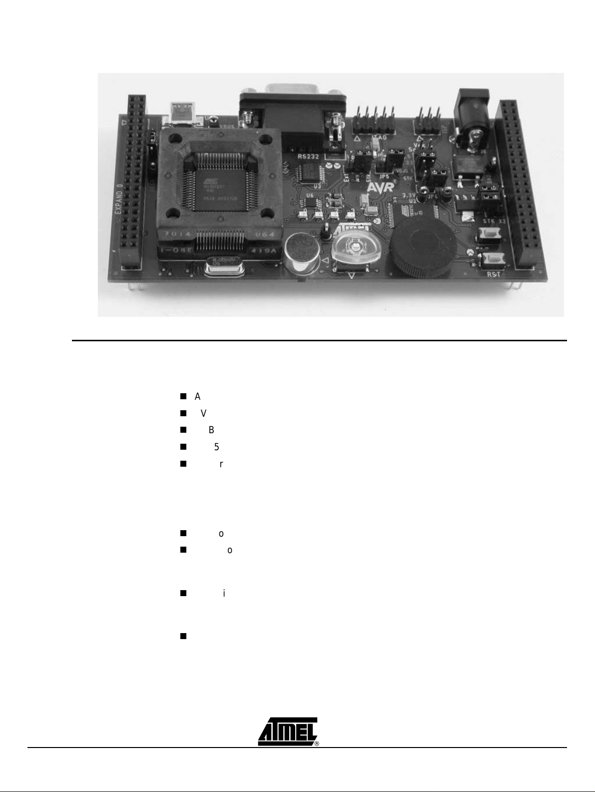
1.1 Overview
Section 1
Introduction
Congratulation for acquiring the A VR® STK525 Starter Kit. This ki t is designed to give
designers a quick start to develop code on the AT90USBxxx and for prototyping and
testing of new designs.
This document describes the STK525 dedicated to the AT90USBxxx AVR
microcontroller. This board is des ig ned to al low an eas y ev alu ation of t he product using
demonstration software.
To complement the evaluation and enable additional development capability, the
STK525 can be plu gged into the Atmel STK500 Start er Kit Board in order to use the
AT90USBxxx with advanced features such as variable VCC, variable VRef, variable
XTAL, etc. and supports all AVR development tools.
To increase its demonstrative capabilities, this stand alone board has numerous onboard resources (USB, RS232, joystick, data-flash, microphone and temperature
sensor).
This user guide acts as a general getting started guide as well as a comple te technical
reference for advanced users.
STK525 Hardware User Guide 1-3
7608A–AVR–04/06
Page 4
Introduction
Figure 1-1 . STK525 Board
1.2 STK525 Starter Kit Feature s
The STK525 provides the following features:
AT90USBxxx TQFP device (2.7V<Vcc<5.5V),
AVR Studio® software interface
USB software interface for Device Firmware Upgrade (DFU bootloader)
STK500 compatible
Power supply flagged by “VCC-ON” LED:
– regulated 3 or 5V,
– from an external power connector,
– from the USB interface (USB device bus powered application),
– from STK5 0 0
ISP connector for on-chip ISP,
JT AG connector:
– for on-chip ISP,
– for on-chip debugging using JTAG ICE,
Serial interfaces:
– 1 USB full/low speed device/host interface
– RS-232C ports with RTS/CTS handshake lines,
On-board resources:
– 4+1-ways joystick,
–4 LEDs,
– temperature sensor,
– microphone,
– serial dataflash memory,
(2)
(1)
,
(2)
,
1-4 STK525 Hardware User Guide
7608A–AVR–04/06
Page 5

Introduction
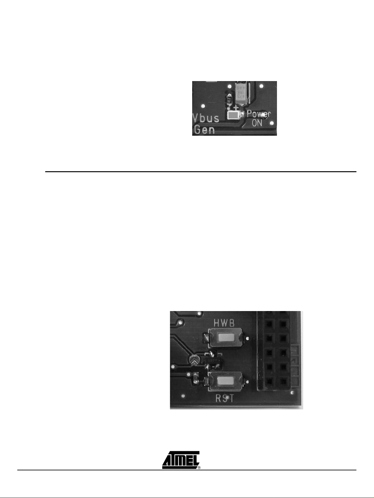
On-board RESET button,
On-board HWB button for force bootloader section execution at reset.
System clock:
– external clock from STK500 expand connectors
– 8 MHz crystal,
Numerous access points for test.
Notes: 1. The STK525 is suppor ted by A VR S tudi o®, ver sion 4.12SP2 or higher . For up-to-date
information on this and other AVR tool products, please consult our web site. The
newest version of AVR Studio®, AVR tools and this User Guide can be found in the
AVR section of the Atmel web site, http://www.atmel.com.
2. ATMEL Flip®, In System Programming Version 3 or Higher shall be used for Device
Firmware Upgrade . Please consult Atmel web site to retrieve the latest version of Flip
and the DFU bootloader Hex file if needed.
STK525 Hardware User Guide 1-5
7608A–AVR–04/06
Page 6
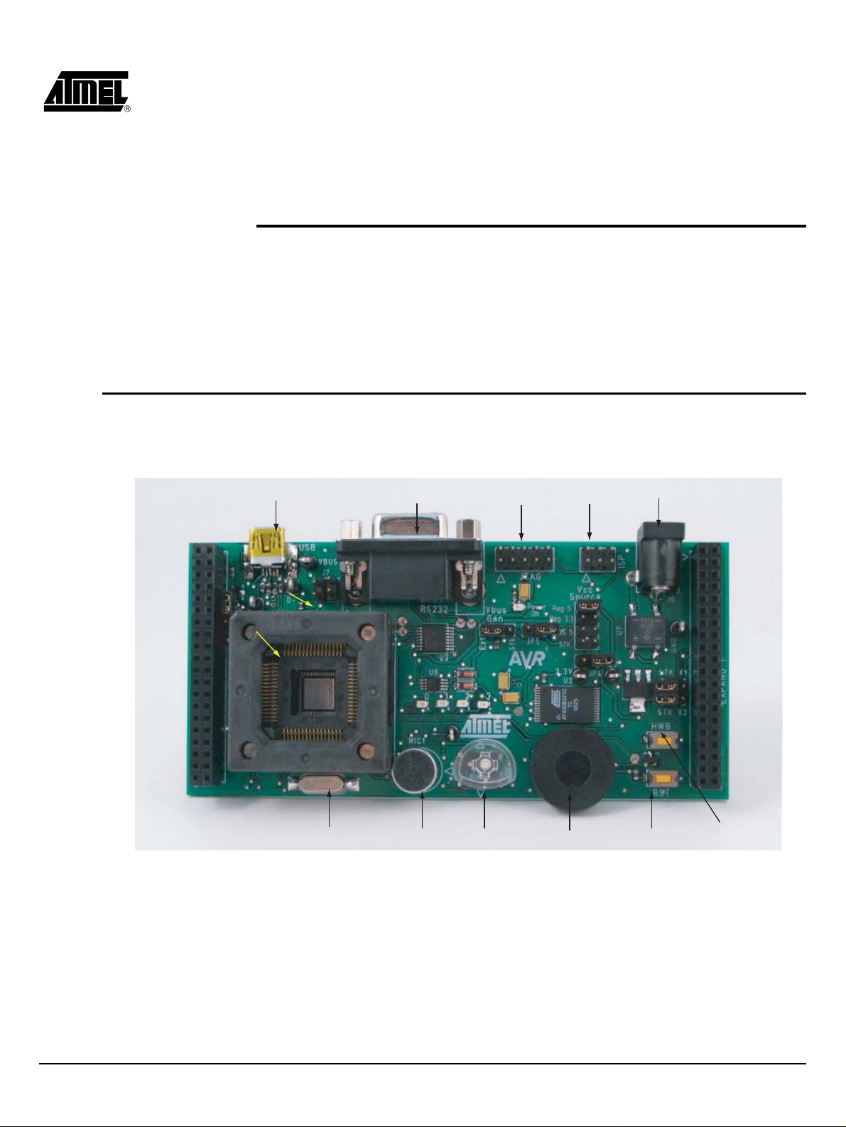
2.1 Overview
Section 2
Using the STK525
This chapter describes the board and all its features.
Figure 2-1 . STK525 Overview
USB MiniAB RS232 JTAG ISP External Power
C Sensor
Pin1
STK500 Expand0
TQFP64 Socket
LEDS
Microphone
Vbus Gen.
Setting
Joystick Potentiometer ResetCrystal
Vcc Src.
Setting
Data Flash
STK500 Expand1
Bootloader
Activation
STK525 Hardware User Guide 2-6
7608A–AVR–04/06
Page 7
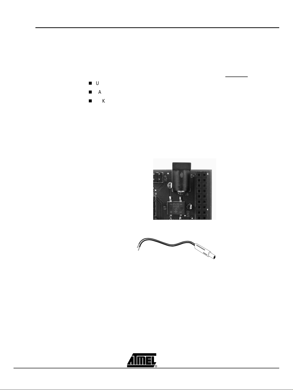
2.2 Power Supply
2.2.1 Power Supply Sources
Using the STK525
The on-board power supply circuitry allows various power supply configurations.
The power supply source can come from three different
USB connector,
JACK PWR connector (J6, See Figure 2-2),
STK500
USB powered: When used as a USB devi ce bus powered application, the STK525 can be powered via
the USB VBUS power supply line.
JACK PWR connector: – Need of a male JACK outlet,
– Input supply from 9 up to 15V
– No specific polarization
(2)
is required.
Figure 2-2 . JACK PWR Connector (J6)
(1)
DC,
(3)
and exclusive sources:
Figure 2-3 . M ale JACK Outlet and Wires
+
-
STK500 Powered: (c.f.
STK525 Hardware User Guide 2-7
“STK500 Resour ces” on page 19).
Notes: 1. 15V is the maxim um level limitation of an unidirectional transit diode.
2. There is a diode (bridge) voltage level between the negative output of the power
supply and the STK525 “GND”. This could introduce some gap of voltage during
measurement and instrumentation.
3. Caution: Do not mount more than one power supply sour ce on STK525.
7608A–AVR–04/06
Page 8
Using the STK525
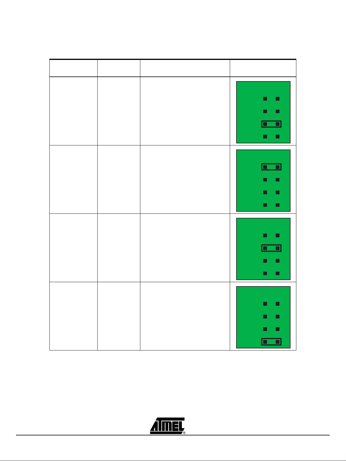
2.2.2 Pow er S upp l y Sett in g
Vcc Source
Jumper position
VBUS 5
REG 5 5V
Table 2-1 . Power Supply
VCC power
supply value
This is the default confi guration.
This should be used for a typical USB
VBUS
(4,7V to 5. 0V)
device “bus powered” application.
In this mod e, the STK525 is powered
directly from th e USB bus, and no
other external power supply is
required.
This configuration can be used for a
USB “self powered” device
application” or when operating has a
USB host.
To use this conf iguration an exter nal
power supply must be connected to
J6 connector.
(1)
Setting
Comments View
Source
Reg 5
Reg 3.3
VBUS 5
STK
Source
Reg 5
Reg 3.3
VBUS 5
STK
VCC
VCC
REG 3.3 3.3V
Depends on
STK
STK500 VTG
setting
Notes: 1. Caution: The STK500 has its own “ON/OFF” switch
This configuration allows the STK525
to be used in a 3V range applicat ion.
This configuration can be used with
both device or host mode USB
applications.
To use this conf iguration an exter nal
power supply must be connected to
J6 connector.
This configuration allows the STK525
to be used with an STK500 board.
In this mode, the STK525 power
supply is generat ed and configured
accord i ng to th e “VT G ” par ameter of
the STK500 (1).
VCC
Source
Reg 5
Reg 3.3
VBUS 5
STK
VCC
Source
Reg 5
Reg 3.3
VBUS 5
STK
2-8 STK525 Hardware User Guide
7608A–AVR–04/06
Page 9
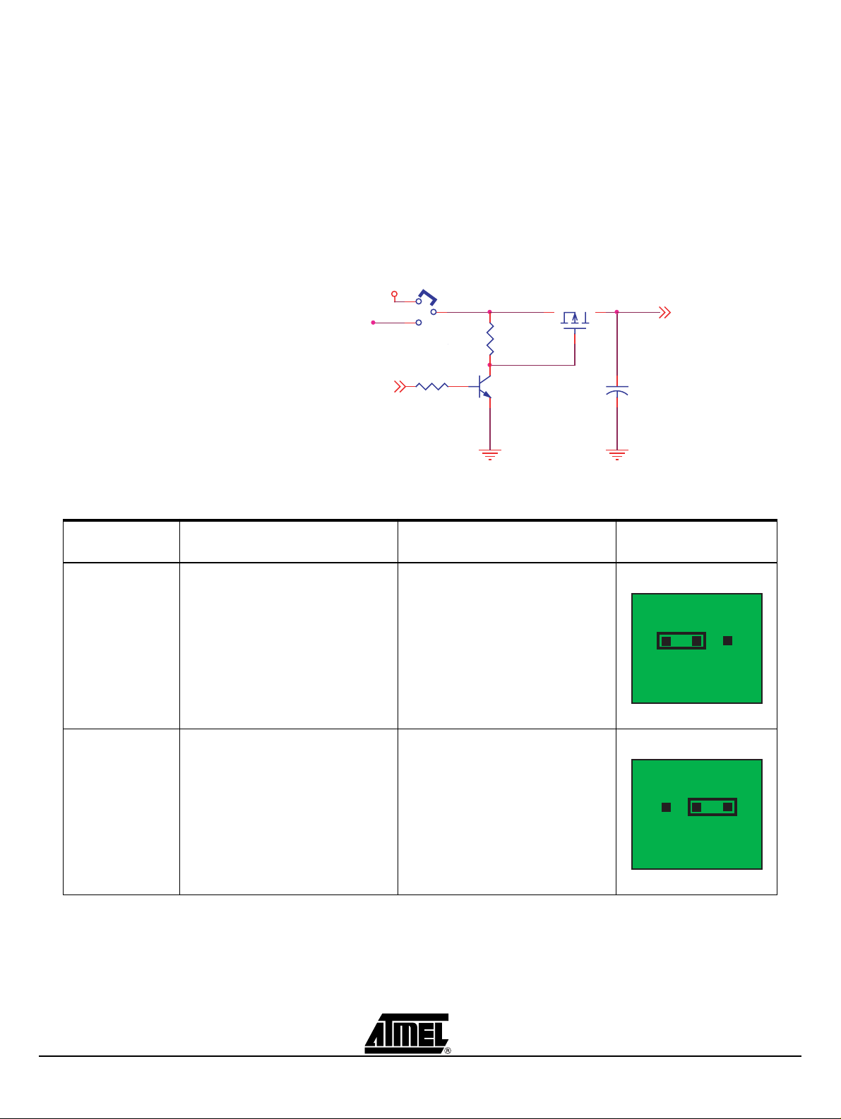
2.2.3 VBUS Generator Setting
Using the STK525
When using the A T90USBxxx microcontroller in USB ho st mode. The STK5 25 should
provide a 5V power supply over the VBUS pin of its USB mini AB connector.
A couple of transistors on the STK525 allows the UVCON pin of the AT90USBxxx to
control the VBUS gene ration (See Figure 2 -4). In this mode the S TK525 is powe red by
external power supply source (J6 or STK500 expand0/1 connectors). JP7 allows to
select the 5V source used by the VBUS generator.
Figure 2-4 . VBUS generator schematic
JP7
VTG
STK
Ext
UVCON
1
3
VBUS ge n
R33
100k
2
R32
10k
Q2
BC847B
FDV304P/FAI
M1
VBUS
C34
4.7uF
-
Table 2-2 . VBUS Generator Setting
“Vbus Gen”
Jumper position
“Ext” Ext e rnal po w er su pp ly from J6
“Stk”
STK525 power supply Comments View
Exte r n a l po w er su pp ly from
Expand0/1 (connected to a STK500)
This is the default configuration.
The VBUS generator source is the
on-board 5V regulator.
The VBUS generator source is the
STK500.
Note:
The “Vtarget” setting of STK500
should be set to “5V”.
Ext
Ext
Vbus
Gen
Stk
Vbus
Gen
Stk
STK525 Hardware User Guide 2-9
7608A–AVR–04/06
Page 10
Using the STK525
2.2.4 “POWER-ON“ LED
2.3 RESET
The POWER-ON LED is always lit when power is applied to STK525 regardless of
power supply source and the regulation.
Figure 2-5 . “VCC-ON” LED
Although the AT90USBxxx has its on-chip RESET circuitry (c.f. AT90USBxxx
Datasheet, section “System Control and Reset), the STK525 provides the AT90USBxxx
a RESET signal which can come from 3 different sources:
2.3.1 Power-on RESET
2.3.2 RESET Push Button
The on-board RC network acts as power-on RESET.
By pressing the RESET push button on the STK525, a warm RESET of the
AT90USBxxx is performed.
Figure 2-6 . RESET Push Button (RST) Implementation
2-10 STK525 Hardware User Guide
7608A–AVR–04/06
Page 11
2.3.3 STK500 RESET
(c.f.
“RESET from STK500” on page 20)
2.4 AT90USBxxx AVR Microcontroller
2.4.1 Main Clock XTAL
To use the USB i nterface of the AT90USBxxx, the clock source should always be a
crystal or external clock oscillator (the internal 8 MHz RC oscillator cannot be used to
operate with the USB interface). Only the following crystal frequency allows proper USB
operations: 2MHz, 4MHz, 6MHz, 8MHz, 12MHz, 16MHz. The STK525 comes with a
default 8MHz crystal oscillator.
When closing ST KX1 and STKX2 s witches, and STK525 is connected to an STK500,
the STK525 can operate with the “STK500 Osc” frequency parameter.
2.4.2 Anal og P ower Supply
Using the STK525
ANA REF By default, AREF is an output of AT90USBxxx.
2.5 Serial Links
2.5.1 USB
AVCC By default, AVCC is equivalent to VCC.
An external AREF source can be chosen (c.f.
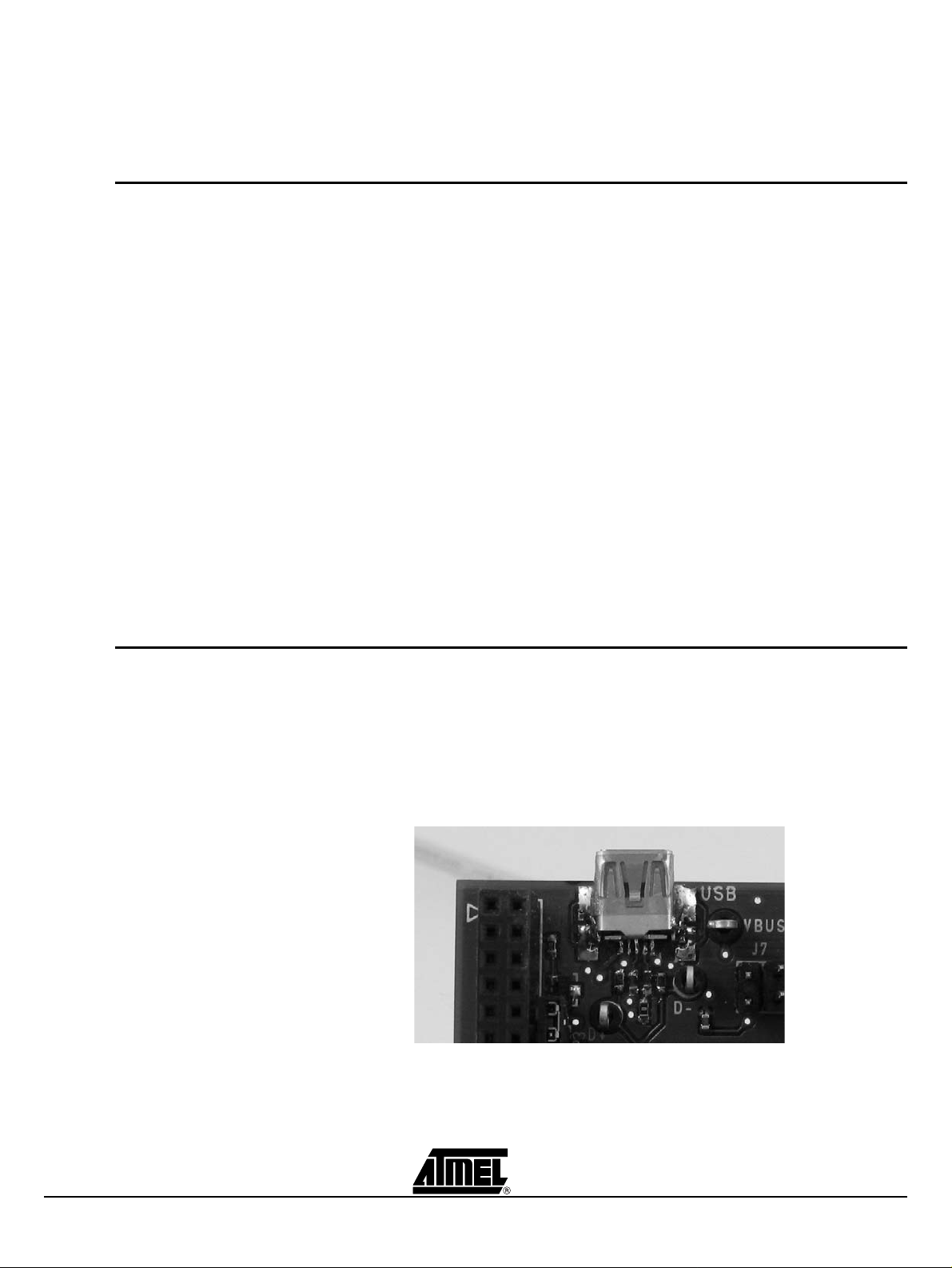
The STK525 is supplied with a standard USB mini A-B receptacle. The mini AB
receptacle allows to connect both a mini A plug or a mini B plug connectors.
Figure 2-7 . USB mini A-B Receptacle
“STK500 Resour ces” on page 19).
When connected to a m ini B plug, the AT90USBxxx opera tes as an “USB device” (the
ID pin of the plug is unconnected) and when connected to a mini A plug, the
AT90USBxxx operates as a “USB host” (the ID pin of the plug is tied to ground).
STK525 Hardware User Guide 2-11
7608A–AVR–04/06
Page 12
Using the STK525
2.5.2 RS-232C
The AT90USBxxx is a microcontroller with an on-chip USART peripheral (USART1).
Only the asynchronous mode is supported by the STK525.
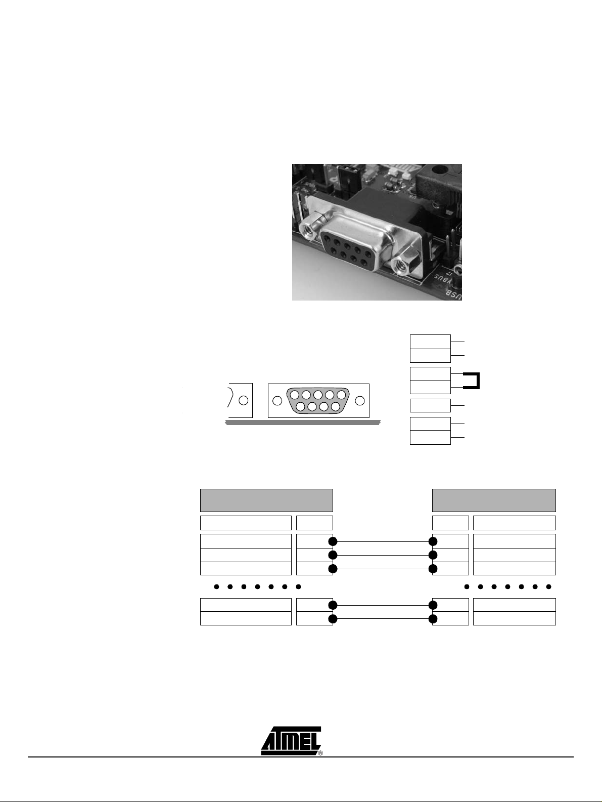
The STK525 is supplied with a RS-232 driver/receiver. One female DB9 connector
assumes the RS-232 connections.
Figure 2-8 . RS -232 DB9 Connector
Figure 2-9 . RS -232 DB9 Connections
RS-232 D B 9 fron t view
5
1
234
69
78
Figure 2-10 . Typical PC Connection Layout
STK525 / RS-232 DB9
Function Pin No Function
RTS (
AT90USBxxx
Pin No
2TxD (AT90USBxxx)
5GND
If Hardware Data Flow Control
7CTS (AT90USBxxx) 7
)
pin 2
RS-TxD
pin 3 RS-RxD
pin 4
pin 6
pin 5 GND
pin 7 RS-CTS
pin 8 RS-RTS
PC / DB9 serial port
(COM1 o r C OM x )
2
3
RxD (PC)
TxD (PC)3RxD (AT90USBxx x)
5 GND
RTS (PC)
8
CTS (PC)8
2-12 STK525 Hardware User Guide
7608A–AVR–04/06
Page 13

Using the STK525
The STK525 USART implement ation allows an optional hardware flow control that can
be enabled thanks to SP4, SP5, SP7, SP8 solder pads (See Figure 2-11).
Figure 2-11 . USART Schematic
VCC
RS232 Interface
U3
16
.
VCC
C1+1V+
C1-
C2+
C2-
RS 232TTL
.
.
.
.
.
GND
15
2
100nF
6
V-
C19
100nF
RS-RxD
13
.
14
.
RS-TxDRS-TxDRS-TxDRS-TxDRS-TxDRS-TxDRS-TxDRS-TxD
RS-CTS
7
.
RS-RTS
8
.
MAX3232
RS232 BUFFER
C18
SP7
SP8
P1
1
6
2
7
3
8
4
9
5
11
10
SUB-D 9 F EMALE
RS232
PD[7..0]
C16
100nF
C17
100nF
RxDPD2
PD3 TXD
SP4
PD1
PD0
CTS
RTS
SP5
3
4
5
12
11
10
9
Table 2-3 . UART Settings
Mode
Software Data Flow
Control
(default configuration)
Optional
Hardwa re Fl ow Control
Note: 1. Tx reference: STK525 source, Rx reference: STK525 destinati on
Solder Pads
Configuration
SP4: open
SP5: open
SP7: open
SP8: open
SP4: close
SP5: close
SP7: close
SP8: close
DB9
Connection
TxRxPin 2
Pin 3
Tx
Pin 2
Rx
Pin 3
CTS
Pin 7
Pin 8
RTS
(1)
STK525 Hardware User Guide 2-13
7608A–AVR–04/06
Page 14

Using the STK525
2.6 On-board Resources
2.6.1 Joystick
The 4+1 way joystick offers an easy user interface implementation for a USB application
(it can emulate mouse movements, keyboard inputs, etc.).
Pushing a push-button causes the corresponding signal to be pulled low, while releasing
(not pressed) causes an H.Z stat e on the s igna l. The user m us t enable i nternal pul l-ups
on the input pins, removing the need for an external pull-up resistors on the push-button.
Figure 2-12 . Joystick Schemati c
SW3
SW3
SW3
1
1
1
2
2
2
TPA511G
TPA511G
TPA511G
Com1
Com1
Com1
Com2
Com2
Com2
Select
Select
Select
Left
Left
Left
Up
Up
Up
Right
Right
Right
Down
Down
Down
PB[7..0]
PB[7..0]
PB[7..0]
PB5
PB5
PB5
5
5
5
PB6
PB6
PB6
7
7
7
PB7
PB7
PB7
3
3
3
PE4
PE4
PE4
6
6
6
PE5
PE5
PE5
4
4
4
PE[7..0]
PE[7..0]
PE[7..0]
2.6.2 LEDs
Figure 2-13 . Joystick Implementation
The STK525 include s 4 green LEDs implemented on one line. They are connected to
the high nibble of “Port D” of AT90USBxxx (PORTD[4..7]).
To light On a LED, the correspo nding port pin must drive to high level. To light Off a
LED, the corresponding port pin must drive a low level. It is the opposite method used in
STK500.
2-14 STK525 Hardware User Guide
7608A–AVR–04/06
Page 15

Figure 2-14 . LEDs Implementation Schematic
In-line Grouped LED s
Using the STK525
R121k
R131k
R141k
R151k
LED 0 (green)
LED 1 (green)
LED 2 (green)
LED 3 (green)
PD4
D2TOPLED LP M676
PD5
D3TOPLED LP M676
PD6
D4TOPLED LP M676
PD7
D5TOPLED LP M676
PD[7..0]
STK525 Hardware User Guide 2-15
7608A–AVR–04/06
Page 16

Using the STK525
2.6.3 Temperature Sensor
The temperature sensor uses a thermistor (R18), or temperature-sensitive resistor. This
thermistor has a ne gative temperature c oefficient (NTC), mea ning the resistance goes
up as temperature goes down. Of all passive temperature measurement sensors,
thermistors have the highest sensitivity (resistance cha nge per degree of temperat ure
change). Thermistors do not have a linear temperature/resistance curve.
The voltage over the NTC can be found using the A/D converter (connected to channel
0). See the AT90USBxxx datasheet for how to use the ADC. The thermistor value (R
T)
is calculated with the following expression:
R
RHV
T
Where: RT = Thermistor value (Ω) at T temperature (°Kelvin)
⋅()VCC V
ADC0
H = Second resistor of the bridge -100 KΩ ±10% at 25°C
R
ADC0 = Volt age value on ADC-0 input (V)
V
VCC = Board power supply
–
()⁄=
ADC0
The NTC thermistor used in STK525 has a resistance of 100 KΩ ±5% at 25° C (T0) and a
beta-value of 4250 ±3%. By the use of the following equation, the temperature (T) can
be calculated:
T
Where: RT = Thermistor value (Ω) at T temperature (°Kelvin)
R
T
⎛⎞
ln
⎝⎠
-------
R
------+
T
0
β
0
β
-------------------------------=
ß = 4250 ±3%
0 = 100 KΩ ±5% at 25°C
R
T
0 = 298 °K (273 °K + 25 °K)
The following cross table also can be used. It is based on the above equation.
Table 2-4 . Thermistor Values versus Temperature
Temp.
(°C)
-20 1263,757 10 212,958 40 50,486 70 15,396
-19 1182,881 11 201,989 41 48,350 71 14,851
-18 1107,756 12 191,657 42 46,316 72 14,329
-17 1037,934 13 181,920 43 44,380 73 13,828
-16 973,006 14 172,740 44 42,537 74 13,347
-15 912,596 15 164,083 45 40,781 75 12,885
-14 856,361 16 155,914 46 39,107 76 12,442
RT
(KΩ)
Temp.
(°C)
T
R
(KΩ)
Temp.
(°C)
T
R
(KΩ)
Temp.
(°C)
T
R
(KΩ)
-13 803,984 17 148,205 47 37,513 77 12,017
-12 755,175 18 140,926 48 35,992 78 11,608
-11 709,669 19 134,051 49 34,542 79 11,215
-10 667,221 20 127,555 50 33,159 80 10,838
2-16 STK525 Hardware User Guide
7608A–AVR–04/06
Page 17
Using the STK525
Temp.
(°C)
R
T
(KΩ)
Temp.
(°C)
T
R
(KΩ)
Temp.
(°C)
T
R
(KΩ)
Temp.
(°C)
-9 627,604 21 121,414 51 31,840 81 10,476
-8 590,613 22 115,608 52 30,580 82 10,128
-7 556,056 23 110,116 53 29,378 83 9,793
-6 523,757 24 104,919 54 28,229 84 9,471
-5 493,555 25 100,000 55 27,133 85 9,161
-4 465,300 26 95,342 56 26,085 86 8,863
-3 438,854 27 90,930 57 25,084 87 8,576
-2 414,089 28 86,750 58 24,126 88 8,300
-1 390,890 29 82,787 59 23,211 89 8,035
0 369,145 30 79,030 60 22,336 90 7,779
1 348,757 31 75,466 61 21,498 91 7,533
2 329,630 32 72,085 62 20,697 92 7,296
3 311,680 33 68,876 63 19,930 93 7,067
4 294,826 34 65,830 64 19,196 94 6,847
5 278,995 35 62,937 65 18,493 95 6,635
6 264,119 36 60,188 66 17,820 96 6,430
T
R
(KΩ)
2.6.4 Microphone
7 250,134 37 57,576 67 17,174 97 6,233
8 236,981 38 55,093 68 16,556 98 6,043
9 224,606 39 52,732 69 15,964 99 5,860
Figure 2-15 . Thermistor Schematic
VCC
PF0
R16
100k
CP1
R18
Temperature
Sensor
The STK525 provides an electret microph one associated with its required preamplifier
(See Figure 2-16), the interface is connected to ADC channel 2 of the AT90USBxxx
microcontroller.
STK525 Hardware User Guide 2-17
7608A–AVR–04/06
Page 18

Using the STK525
Figure 2-16 . Microphone interface schematic
3.3V
R20
2.2k
MIC1
MICROPHONE
2.6.5 Data Flash Memory
R23 100k
3.3V
R24 100k
-
6
+
5
8 4
U4B
LMV358
7
R27 0
C24 4.7uF
+
R21
100k
R25 10k
R28
100k
+
1uF
C25
2
3
3.3V
C22 220pF
U4A
LMV358
-
1
+
8 4
R22
100k
R26 22k
For mass-storage class demonstration purposes, the STK525 provides an on-chip serial
Flash memory (AT45DB321x) connected to the AT90USBxxx Serial Port Interface
(SPI).
TP4
1
Mic
2.6.6 Potentiometer
The data-flash chip select signal is connected to PortB bit 4 of the AT90USBxxx (See
Figure 2-17).
Figure 2-17 . On-board data flash schematic
PB[7..0]
3.3V
R10
100k
PB4
PB1
PB2
PB3
R11
100k
RESET
U2
1
BUSY
2
RESET
3
WP
11
CS
12
SCK
13
SI
14
SO
AT45DB321C TSOP28
VCC
GND
3.3V
6
C15
7
100nF
The cursor of a potentiometer is connected to ADC channel 1 of the AT90USBxxx.
2-18 STK525 Hardware User Guide
7608A–AVR–04/06
Page 19
2.7 STK500 Resources
Using the STK525
Figure 2-18 . Connecting STK525 to the STK500 Board
Note: Caution: Do not mount an AVR microcontroller on the STK500 board when STK525 is
plugged on STK500.
2.7.1 Supply Voltage from STK500
The AVR supply voltage coming from STK500 (VT G) can also be controlled from AVR
Studio®.
The supply voltage coming from STK500 is controlled by power supply circuitry of
the STK525. Refer to
Table 2-1 on page 8 to configure “Vcc Source” jumper.
2.7.2 Analog Reference Voltage from STK50 0
The AVR Analog Reference V oltage com ing from ST K500 (RE F) can also be cont rolled
from AVR Studio®.
JP3 should be closed
STK525 Hardware User Guide 2-19
7608A–AVR–04/06
Page 20
Using the STK525
2.7.3 EXP.CON 0 & EXP.CON 1 Connectors
Figure 2-19 . EXP.CON 0 and EXP.CON 1 Connectors
2.7.4 Main Clock from STK500
The AVR clock frequency (external) coming from STK500 (XT1/XT2) can also be
controlled from AVR Studio®.
GND GND1 2
n.c. (AUXI0) n.c. (AUXO0)3 4
n.c. (CT7) n.c. (CT6)5 6
n.c. (CT5) n.c. (CT4)7 8
n.c. (CT3) n.c. (CT2)9 10
n.c. (CT1) n.c. (BSEL2)11 12
n.c. REF13 14
NRST PG215 16
PG1 PG017 18
GND GND19 20
VTG VTG21 22
PC7 PC623 24
PC5 PC425 26
PC3 PC227 28
PC1 PC029 30
PA7 PA631 32
PA5 PA433 34
PA3 PA235 36
PA1 PA037 38
GND GND39 40
EXP. CON 0
GND GND1 2
n.c. (AUXI1) n.c. (AUXO1)3 4
n.c. (DATA7) n.c. (DATA6)5 6
n.c. (DATA5) n.c. (DATA4)7 8
n.c. (DATA3) n.c. (DATA2)9 10
n.c. (DATA1) n.c. (DATA0)11 12
n.c. (SI) n.c. (SO)13 14
n.c. (SCK) n.c. (CS)15 16
XT1 XT21718
VTG VTG1920
GND GND2122
PB7 PB623 24
PB5 PB425 26
PB3 PB227 28
PB1 PB029 30
PD7 PD63132
PD5 PD43334
PD3 PD23536
PD1 PD03738
GND GND3940
EXP. CON 1
T op View
“STKX1” and ”STKX2” jumpers should be closed
2.7.5 RESET from STK500
The AVR RESET coming from STK500 (NRST - EXP.CON 0) can also control the
STK525. STK525 is protected against +12V RESET pulse (parallel programing not
allowed for AT90USBxxx on STK525) coming from STK500.
2.8 In-System Programming
2.8.1 Programming with USB bootloader: DFU (Devi ce Firmware Upgrade)
AT90USBxxx part comes with a default factory pre-programmed USB bootloader
located in the on-chip boot section of the AT90USBxxx. This is the easiest and fastest
way to reprogram the device directly over the USB interface. The “Flip” PC side
application available for free on Atmel website offers a flexible and user friendly
interface to reprogram the application over the USB bus.
2-20 STK525 Hardware User Guide
7608A–AVR–04/06
Page 21

The HWB pin of the A T90USB xx x allows to forc e the boot load er sec tion exec ution after
reset. (Refer to AT90USBxxx datasheet section “boot loader support”). To force
bootloader execution, operate as follows:
Press both “RST” and “HWB” push buttons
First release the “RST” push button
Release the “HWB” push button
For more information about the USB bootloader and FLIP software, please refer to the
‘USB bootloader datasheet’ document and ‘FLIP User Manual’.
2.8.2 P rogramming with AVR ISP mkII Programmer
The AT90USBxxx can be programmed using specific SPI serial links. This sub section
will explain how to connect the programmer.
The Flash, EEPROM and all Fuses and Lock Bits options ISP-programm able can be
programmed individually or with the sequential automatic programming option.
The AVR ISP mkII progra mmer is a com pact an d easy-to-use In-System P rogramming
tool for developing applications with AT90USBxxx. Due to the small size, it is also an
excellent tool for field upgrades of existing applications.
Using the STK525
The AVR ISP programming interface is integrated in AVR Studio®.
To program the device using AVR ISP programmer, connect the 6-wire cable on the ISP
connector of the STK525 as shown in Figure 2-20.
Note: See AVR Studio® on-line Help for informati on.
Figure 2-20 . Programming from AVR ISP mkII programmer
2.8.3 Programmin g with STK500
The AT90USBxxx can be programm ed using the serial program ming mode in the A VR
Studio STK500 software. The software interface (In-System Programming of an external
target system) is integrated in AVR S tud i o ®.
STK525 Hardware User Guide 2-21
7608A–AVR–04/06
Page 22
Using the STK525
To program the dev ice using ISP f rom STK500, conne ct the 6-wire cable between the
ISP6PIN connector of the STK500 board and the ISP connector of the STK525 as
shown in Figure 2-18.
Note: See AVR Studio® on-line Help for informati on.
Note: The high voltage parallel programming mode with STK500 is not available for an
STK525. To reprogram an AT90USBxxx part in parallel mode, use an STK501 extension
board (AT90USBxxx product pinout is compatible with the STK501 parallel programing
mode).
2.8.4 Programming with A VR JTAG ICE
The AT90USBxxx can be programmed using specific JTAG link. This sub-section will
explain how to connect and use the AVR JTAG ICE.
Note: When the JTAGEN Fuse is unprogrammed, the four TAP pins are normal port pins, and
the TAP controller is in reset. When programmed, the input TAP signals are internally
pulled high and the JTAG is enabled for Boundary-scan and programming. The
AT90USBxxx device is shipped wit h this fuse programmed.
Figure 2-21 . Connecting AVR JTAG ICE to STK525
The Flash, EEPROM and all Fuse and Lock Bit options ISP-programmable can be
programmed individually or with the sequential automatic programming option.
Note: See AVR Studio® on-line Help for informati on.
2-22 STK525 Hardware User Guide
7608A–AVR–04/06
Page 23
2.9 Debugging
2.9.1 Debugging with AVR JTAG ICE mkII
Every STK525 can be used for debugging with JTAG ICE MK II.
Connect the JTAG ICE mkII as shown in Figure 2-21, for debugging help, please refer to
AVR Studio® Help information.
When using JTAG ICE MK II for debugging, and as AT90USBxxx parts are factory
configured with the higher security level set, a chip erase operation will be performed on
the part before debugging. Thus the on-ch ip flash bootloader will be erased. It can be
restored after the debug session using the bootloader hex file available from ATM EL
website.
2.10 Test Points
There are 8 test points implemented, these test points are referred in the full schematics
section.
Using the STK525
Config.
Pads
Reference
T1 D+ USB D+ data line
T2 D- USB D- data line
T3 Aref Analog reference
T4 Mic Microphone preamplifier output
T5 3.3V 3.3V internal power supply
T6 5V 5V inter nal power supply
T7 Gnd Ground
T8 Vbus USB Vbus power supply
Related Signals Function
STK525 Hardware User Guide 2-23
7608A–AVR–04/06
Page 24
Using the STK525
2.11 Configuration Pads
Configuration pads are used to disconnect/connect on-board peripherals or elements, their
default configuration is: connect.
2.11.1 Confi guration P ads Listing
Table 2-5 . Configuration Pads
Config.
Pads
Reference
CP1 °c sensor (PF0)
CP2 pot. (PF1)
CP3 Mic.(PF2)
2.11.2 Configuration Pads - Disconnection
Figure 1. Configuration Pad - Disconnection
2.11.3 Confi guration P ads - Co nn e ct i on
Related
Signals
Function
This configuration pad is used to disconnect/connect the
CTN sensor from STK525.
This configuration pad is used to disconnect/connect the
potentiomet er from STK525.
This configuration pad is used to disconnect/connect the
microphone preamplifier output from STK525.
Cut Connection
Figure 2. Configuration Pad - Re-connection
WireDroplet of So lder
2-24 STK525 Hardware User Guide
7608A–AVR–04/06
Page 25
2.12 Solder Pads
2.12.1 Solder Pads Listing
Using the STK525
Solder pads are used to disconnect/connect on-board peripherals or elements, their default
configuration is: disconnect.
Table 2-6 . Solder Pads
Solder.
Pads
Reference
SP1 AVCC/VCC This solder pad can be used to bypass L1.
SP2 NRST/RESET This solder pad can be used to bypass D1.
SP3 3.3V
SP4 PD1/CTS
SP5 PD0/RTS
SP6 VBUS This solder pad allows to bypass U5 VBUS current limit er.
SP7 RS-CTS
SP8 RS-RTS
Related
Signals
Function
This solder p ad is reserved to connect 3.3V power supply to
the N.C pin of Expand0/1
This solder pa d all ows to enable the logical CTS signal for
hardware contro l flow on RS232 interface.
This solder pa d all ows to enable the logical R TS signal for
hardware contro l flow on RS232 interface.
This solder pa d all ows to enable the physical CTS signal for
hardware contro l flow on RS232 interface.
This solder pa d all ows to enable the physical R TS signal for
hardware contro l flow on RS232 interface.
STK525 Hardware User Guide 2-25
7608A–AVR–04/06
Page 26

Troubleshooting Guide
Figure 3-1 . Troubleshooting Guide
Problem Reason Solution
Section 3
The Green “VCC-ON”
LED is not on
STK525 does not work
The A T90USBxxx cannot
be programmed
AVR Studi o does not
detect the AVR tool used
No power supply
The
STK500 ISP header
is not connected.
The A VR ISP probe is
not connected
The A V R JTAG ICE
probe is not
connected
The memory lock bits
are programmed
The fuse bits are
wrongly programmed
Programming too fast
with ISP SPI
Serial/USB cable is
not connected, or
power is off
PC COM port is in
use
Verify the power supply source
Verify the power supply source
Connect the DC power supply source, o r
USB interface or STK500.
Connect a 6-pin flexible cable from
STK500 ISP 6-PIN header to the correct
STK525 ISP header (page 21)
Connect the AVR ISP 6-PIN header to
the correct STK525 ISP header (page
21)
Connect the JTAG ICE 10-PIN header to
the correct STK525 JTAG header (page
22)
Erase the memory before programming
Check the fuse bits
Check oscillator settings and make sure
it is not set higher than SPI clock
Connect seri al cable to RS232 (STK5 00 AVR ISP) and check power connect ions
Connect serial cable to USB (JATG ICE
MKII, AVR ISPmkIIl) and chec k power
connections
Disable other programs that are using
PC COM port.
Change PC COM port
AVR Studio does not
detect COM port.
STK525 Hardware User Guide 3-26
Disable COM port auto-detection in AVR
St udio file menu. Force COM port to
correct COM port
7608A–AVR–04/06
Page 27

Troubleshooting Guide
STK525 Hardware User Guide 3-27
7608A–AVR–04/06
Page 28

Section 4
Technical Specifications
System Unit
– Physical Dimensions ................................................. L=119 x W=56 x H=27 mm
– Weight...........................................................................................................70 g
Operating Conditions
– Internal Voltage Supply .............. ........................ ...............................2.7V - 5.5V
– External Voltage Supply ..........................................................9V -15V (100mA)
Connections
– USB Connector......................................................................Mini AB receptacle
– USB Communications .......................................................Full speed/low speed
– RS 232C Connector.............................................................9-pin D-SUB female
– RS 232C Communications Maximum Speed........................................250 kbps
STK525 Hardware User Guide 4-28
7608A–AVR–04/06
Page 29

Section 5
Technical Support
For Technical support, please contact avr@atmel.com. When requesting technical
support, please include the following information:
Which target AVR device is used (complete part number)
Target voltage and speed
Clock source and fuse setting of the AVR
Programming method (ISP, JTAG or specific Boot-Loader)
Hardware revisions of the AVR tools, found on the PCB
Version number of AVR Studio. This can be found in the AVR Studio help menu.
PC operating system and version/build
PC processor type and speed
A detailed description of the problem
STK525 Hardware User Guide 5-29
7608A–AVR–04/06
Page 30

Section 6
Complete Schematics
On the next pages, the following documents of STK525 revision 4381A are shown:
Complete schematics,
Asse m bly drawing,
Bill of mater ials .
Default configuration summary
STK525 Hardware User Guide 6-30
7608A–AVR–04/06
Page 31

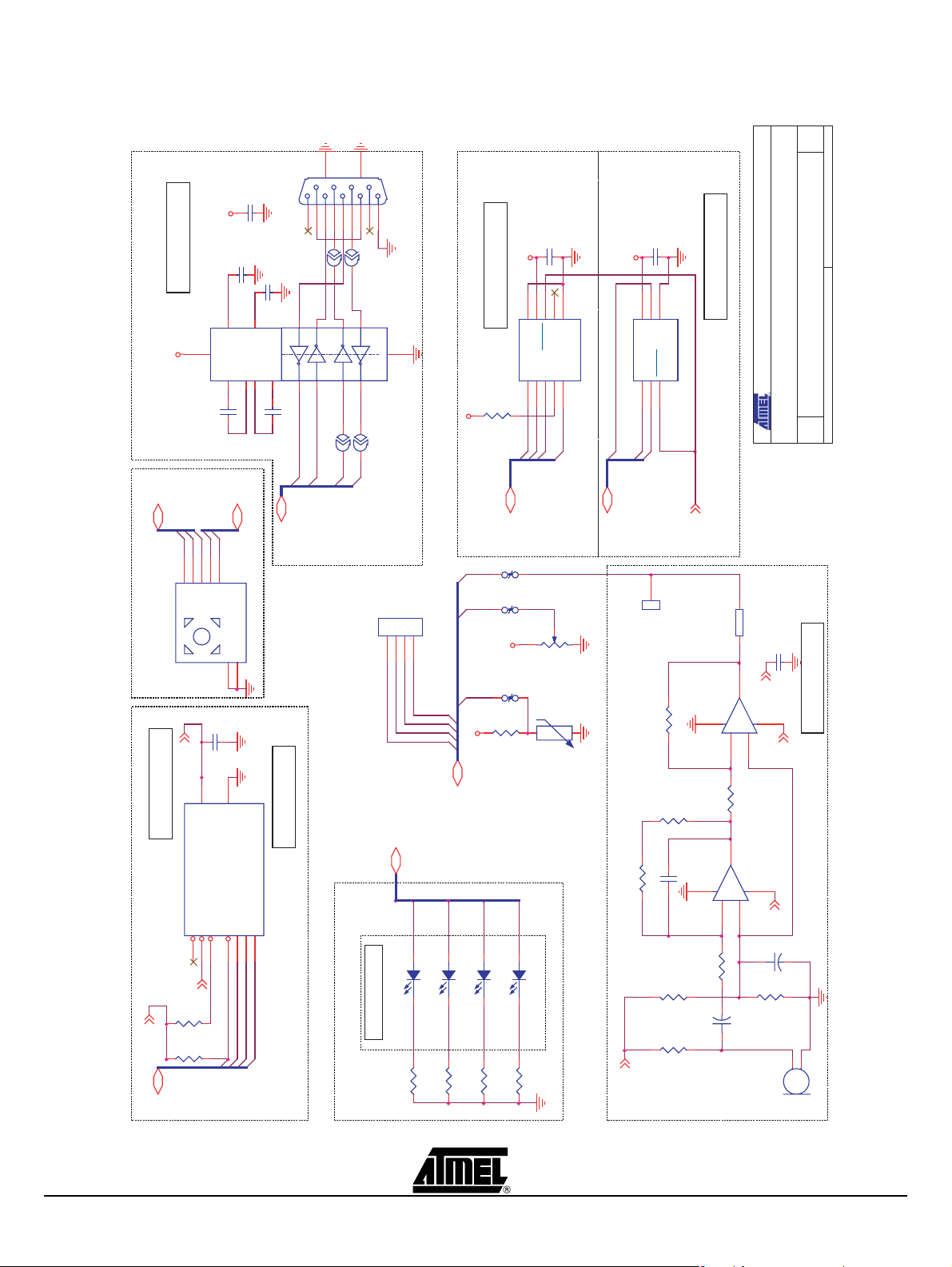
Figure 6-1 . Schematics, 1 of 5
Complete Schematics
PE2
C8
220nF
C1
100nF
VCC
C6
100nF
VCC
C5
100nF
VCC
R3
47k
SW1
HWB
VCC
VCC
Force Bootloader Execution
DECOUPLING CAPACITORS
CLOSED TO THE DEVI C E
DECOUPLING CAPACITORS
CLOSED TO THE DEVI C E
MCU Pin52
DECOUPLING CAPACITORS
CLOSED TO THE DEVI C E
MCU Pin21
MCU Pin3
PC[7..0]
Reset Circuit
PC1
PB3
CR2
CR1
PC0
PC035PC136PC237PC338PC439PC540PC641PC7
PB4
PC[7..0]
PE1
PE0
34
PE033PE1
PD7
PD6
PD5
PD4
PD3
PD2
PD1
PD0
XTAL1
XTAL2
GND
VCC
RESET
PE5
PE4
PB7
16
PB5
PB6
R4 0
PGB0010603
PGB0010603
PD[7..0]
U1
UGND
UCAP C apac it or
PD[7..0]
32
PD7
31
PD6
30
PD5
29
PD4
28
PD3
27
PD2
26
PD1
25
PD0
24
XTAL1
23
XTAL2
22
21
20
19
18
17
PB7
Closed t o t he MCU
PE5
PE4
PB[7..0]PB[7..0]
VCC
RESET
PE7
PE3
PE2
PE1
PE0
PB[7..0]
PE[7..0]
PA[7..0]
PA3
PA4
PA5
PA6
PA7
PE2
PC7
PC6
PC5
PC4
PC3
PC2
PA[7..0]PA[7..0]PA[7..0]
PA[7..0]PA[7..0]PA[7..0]
PA2
PA1
PA0
VCC
AREF
PF[7..0]
C3
100nF
SP1
L1
BLM -21A 102S
VCC AVCC
C2
100nF
Ferrite & c apac it ors
closed t o t he MCU
PF7
PF6
PF5
PF4
PF3
PF2
PF1
PF0
AGND
AVCC
C4
100nF
AREF
48
PA2
49
PA1
50
PA0
51
VCC
52
GND
53
PF7
54
PF6
55
PF5
56
PF4
57
PF3
58
PF2
59
PF1
60
PF0
61
AREF
62
GND
63
AVCC
64
1
UVCON
D+ D- R ESI STORS
Closed t o t he MCU
42
43
PE2
PA744PA645PA546PA447PA3
AT90USB128
PE72UVcc3D-4D+5UGND6UCAP7VBUS8PE39PB010PB111PB212PB313PB414PB515PB6
PE6
PB0
PB1
PB2
UVCON PE7
VCC
J1
VBUS
D+
D-
UID PE3
UCAP
UVCC
VBUS
C7
1uF
UCAP
R2 22
R1 22
VBUS
VBUS
2-D-
1-V_BUS
UGND UGNDUGNDUGNDUGND
4-ID
3-D+
SHIELDSHIELDSHIELDSHIELD
5-GND
USB_MiniABF
RESET
of
RESET
C9
220nF
Close Solder Pad
To use parallel prog mode
BAT54/SOT
SP2
(12V on Reset Pin)
STK525 MEZZANINE FOR STK500
Title
AREF
1
TP3
AREF
D-
1
TP2
D-D+
D+
1
TP1
R7 0
R6 0
RESISTORS
UGND
AGND
SW2
R5
D1
XTAL1
XTAL2
Ext Reset
47k
NCKA
INT 0/2
NRST
15pF
8MHz C11
Y1
C10
15pF
Important Note:
U1 is mounted through a TQFP64 ZIF socket
14Wednesday , February 15, 2006
11.0
CPU
A4
Size Docum ent N um ber Rev
Date: Sheet
CLOSED TO THE DEVI C E
STK525 Hardware User Guide 6-31
7608A–AVR–04/06
Page 32

Complete Schematics
R8
Figure 6-2 . Schematics, 2 of 5
of
24Tuesday , J anuary 17, 2006
C12
1nF
PE[2..0]
PC[7..0]
PB[7..0]
VTG
AREF
PD[7..0]
2k
Q1
BC847B
PD[7..0]
JP3
STK AREF
1 2
R9
10k
C14
100nF
PE[2..0]
PA[7..0]
STK525 MEZZANINE FOR STK500
<Doc> 1.0
PC[7..0]
PA[7..0]
PB[7..0]
STK500 Expand connect ors
A4
Title
Size Docum ent N um ber Rev
Date: Sheet
PE0
PE2
PC6
PC4PC5
PC2
REF
VTG
6
8
10
16
18
12
14
4
2
CT6
CT4
CT2
PE2
PE0
GND
NRST
J3
GND
1
3
VTGVTG
REF
BSEL2
AUXO0
AUXI0
CT7
CT5
CT3
CT1
(n.c.)
NRST
PE1
5
7
9
11
13
15
17
STKNC
PE1
PC0PC1
PA0
PA4
PA2
32
34
36
22
24
26
28
20
VTG
PC6
PC4
GND
GND
VTG
PC7
PC5
19
21
23
25
27
PC3
PC7
38
30
PC2
PC3
29
40
PA6
PA4
PA2
PA0
PC0
PC1
31
PA7 PA6
PA7
33
PA5
PA5
35
PA3
PA3
37
PA1
PA1
GND
CON 2x20
EXP. CON 0
GND
39
XTAL2
XT2XT1
PB6
PB2
PB4
PB0
PD6
PD2
PD4
PD0
JP2
STK X2
1 2
XTAL1
6
8
10
12
2
4
GND
DATA6
DATA4
DATA0
AUXO1
J2
GND
AUXI1
DATA7
DATA5
DATA3
1
3
5
7
9
22
14
16
18
24
26
28
30
20
SO
CS
XT2
PB6
PB4
PB2
VTG
GND
DATA9
DATA1
SI
SCK
XT1
VTG
GND
PB7
PB5
PB3
11
13
15
17
19
21
23
25
27
29
PB0
PB1
40
32
34
36
38
PD6
PD4
PD2
PD0
GND
CON 2x20
PD7
PD5
PD3
31
33
35
37
EXP. CON 1
PD1
GND
39
PD5
PD7
PD1
VTG
JP1
STK X1
1 2
100nF
C13
PB7
PB5
PB3
PB1
PD3
SP3
STKNC
3.3V
Important:
Def ault c onf iguration: open
reserv ed f or f ut ure m as s s t orage ex t ens ion
6-32 STK525 Hardware User Guide
7608A–AVR–04/06
Page 33
VCC
DECOUPLING CAPACITOR
CLOSE TO THE DEVIC E
VCC
C18
2
V+
.
16
VCC
C1+
U3
1
C16
RS232 Interface
Figure 6-3 . Schematics, 3 of 5
10
11
C20
100nF
100nF
6
C1-3C2+4C2-
100nF
P1
SP7
RS-CTS
RS-TxDRS-TxDRS-TxDRS-TxDRS-TxDRS-TxDRS-TxDRS-TxD
RS-RxD
C19
100nF
.13.
V-
RS 232TTL
5
12
RxDPD2
C17
100nF
RS-RTS
7
14
.11.
.10.
CTS
SP4
PD1
PD3 TXD
SUB-D9 F EMALE
RS232
594837261
SP8
SP5
RS232 BUFFER
MAX3232
.
15
GND
.8.
9
RTS
PD0
JTAG Interface
VCC
6
2
4
DECOUPLING CAPACITOR
CLOSE TO THE CONN EC TOR
VCC
GND
J4
TCK
TDO
1
3
R17
VCC
5
0
PF4PF4
PF6
PF5PF5
C21
8
RESET
TMS
7
100nF
10
n.c.
VCC
9
PF7
GND
CON 2x5
TDI
Serial ISP
Interface
VCC
2
J5
JTAG CON
1
PB2
PB3
Complete Schematics
of
34Tuesday , J anuary 17, 2006
C23
100nF
DECOUPLING CAPACITOR
6
4
PDI
VCC
GND
CON 2x3
PDO
SCK
RESET
5
3
RESET
PB1
CLOSE TO THE CONN EC TOR
ISP CON
STK525 MEZZANINE FOR STK500
<Doc> 1.0
Interfaces
A4
Title
Size Document N um ber Rev
Date: Sheet
PB[7..0]
PB5
PB6
5
7
Select
SW3
PE[7..0]
PB7
PE4
PE5
3
6
4
Up
Left
Right
Down
Com11Com2
TPA511G
2
Joystick Interface
C15
100nF
3.3V
7
6
VCC
BUSY1RESET2WP
3
GND
CS11SCK12SI13SO
14
DECOUPLING CAPACITOR
CLOSE TO THE DEVIC E
U2
Data Flash
R11
100k
RESET
PB1
PB2
3.3V
R10
100k
PB[7..0]
PB4
PB3
PD[7..0]
Caution D at aF las h
AT45DB321C TSOP28
Fix 3V Power supply Only
LEDs
PF[7..0]
PF2
CP3
PF1
J7
123
4
PF0
PF1
PF2
PF3
PF Spare (Not m ount ed)
PD[7..0]
PD4
PD5
D2TOPLED LP M676
LED 0 (green)
In-line Grouped LEDs
LED 1 (green)
R121k
R131k
CP2
VCC
R19
CP1
PF0
VCC
PF[7..0]
R18
R16
100k
Temp Sensor
PD7
PD6
D3TOPLED LP M676
D4TOPLED LP M676
D5TOPLED LP M676
LED 2 (green)
LED 3 (green)
R141k
R151k
POT 100k
PB[7..0]
1
TP4
NCP18WF104J03RB
Microphone Preamplifier Interface
R23 100k
3.3V
R24 100k
Mic
R22
100k
C22 220pF
R21
R20
2.2k
100k
RESET
U4A
U4B
LMV358
-
R25 10k
C24 4.7uF
LMV358
R26 22k
2
+
R27 0
-
6
1
+
C26
100nF
7
3.3V
+
8 4
5
3.3V
8 4
3
3.3V
C25
+
R28
100k
MIC1
1uF
DECOUPLING CAPACITOR
CLOSE TO THE DEVIC E
MICROPHONE
STK525 Hardware User Guide 6-33
7608A–AVR–04/06
Page 34
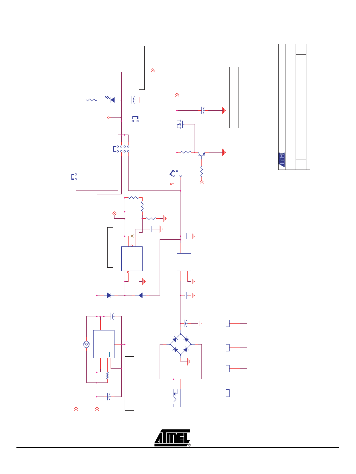
Complete Schematics
Figure 6-4 . Schematics, 4 of 5
UCAP
JP Clos ed f or 3.0<Vcc <3.3
C30
1 2
STK
VCC
3 4
VBUS
5 6
3.3V
3.3V
7 8
Ext
4.7uF
-
JP5
12
VCC Source
R35
100k 1%
R30100k 1%
R31
124k 1%
D8
TOPLED LP M676
R34
1k
3.3V
JP not m ount ed,
JP4
reserv ed f or f uture mas s s t orage ex t ens ion
in stand alone m ode
1 2
POWER LED(RED)
VCC
JP6
3.3V
VBUS
C34
4.7uF
-
VBUS generator f or OTG/HOST mode
FDV304P/FAI
M1
Q2
10k
BC847B
R33
VBUS g e n
100k
UVCON
R32
2
JP7
1
3
VTG
STK
Ext
5V5V
1F <Cap Vbus < 6F OTG Specif ic at ion
STK525 MEZZANINE FOR STK500
Title
of
44Tuesday , J anuary 17, 2006
<Doc> 1.0
POWER
A4
Size Document N um ber Rev
Date: Sheet
4
CC
SET
OUT
OUT
FAULT
U6out=1.25*(1+R28/R29)
U6
IN2GND
SHDN
7
D6
LL4148
C28
4.7uF
6
OUT18OUT27OUT3
GND
SP6
U5
IN12IN23EN4OC
VTG
VBUS
1
TPS2041A
5
R29
10k
C27
100nF
TPS2041A Vbus Icc limiter optionnal
3
D7
LL4148
When Not Mounted C los e Solder Pad
LP3982
U7
3
J6
C33
100nF
OUT
U8
IN
GND
LM340
C32
220nF
4.7uF
C31
-
1
4
-+
2
321
Ext Power Supply
CONNECTOR JACK PWR
DF005S
VBUS
1
TP8
VBUS
GND
1
TP7
5V
1
TP6
TP5
5V
3.3V
1
3.3V
C29
33nF
8
6
5
1
6-34 STK525 Hardware User Guide
7608A–AVR–04/06
Page 35
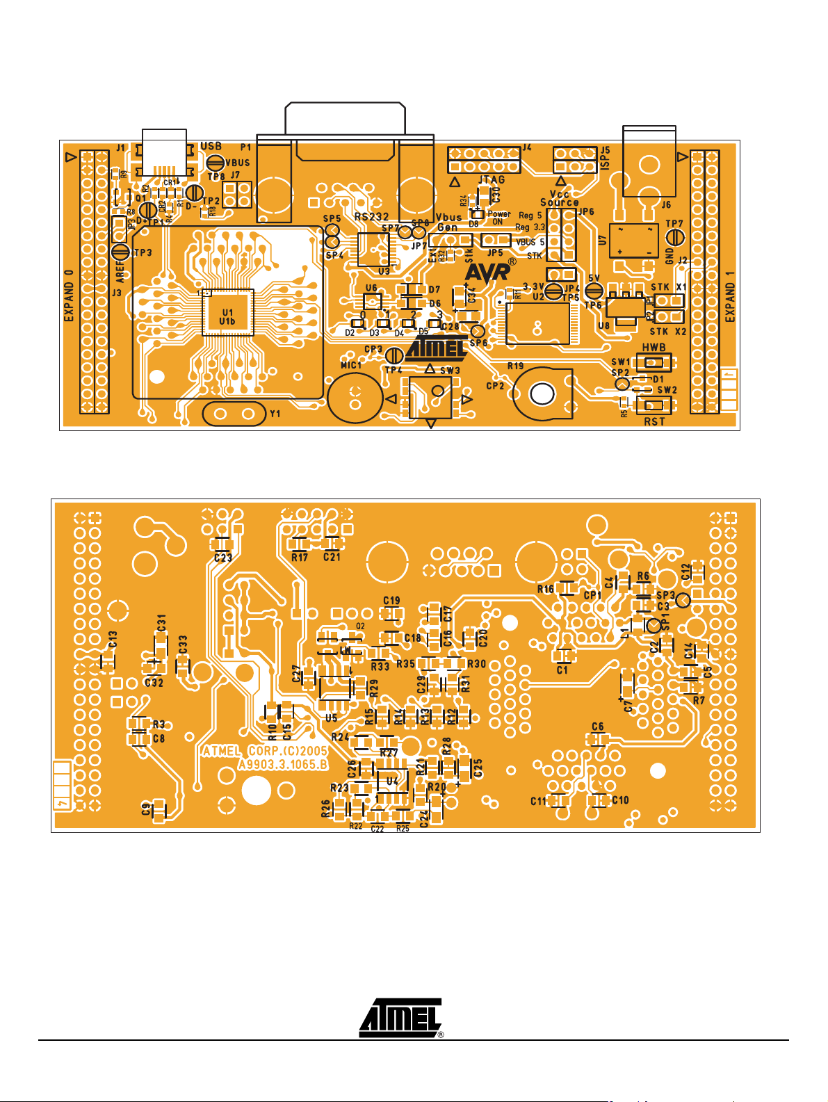
Figure 6-5 . Assembly Drawing, 1 of 2 (component side)
Complete Schematics
Figure 6-6 . Assembly Drawing, 2 of 2 (solder side)
STK525 Hardware User Guide 6-35
7608A–AVR–04/06
Page 36

Complete Schematics
Table 6-1 . Bill of material
Item Q.ty Reference Part Tech. Characteristics Package
1 2 CR1,CR2 PGB0010603 ESD protection CASE 0805
219
3 2 C7,C25 1uF 10Vmin ±10% EIA/IECQ 3216
4 3 C8,C9,C32 220nF 50V-10% Ceramic CASE 0805
5 2 C10,C11 15pF 50V-5% Ceramic CASE 08 05
6 1 C12 1nF 50V-5% Ceramic C ASE 0805
7 1 C22 220pF 50V-5% Ceramic CASE 0805
8 5 C24,C28,C30,C31,C34 4.7uF 10Vmin ±10% EIA/IECQ 3216
9 1 C29 33nF 50V-5% Ceramic CASE 08 05
10 3 CP1, CP2, CP3 Config uration Pad
11 1 D1 BAT54/SOT Vf=0.3V SOT23
12 5 D2,D3,D4,D5,D8 TOPLED LP M676
13 2 D6,D7 LL4148 i=200mA max LL-34
14 5 JP1,JP2,JP3,JP4,JP5 JUMPER 1x2 Need 1 shunt 0,1" pitch
15 1 J1 USB_MiniABF
C1,C2,C3,C4,C5,C6,C13,C14,C15,C16,C
17,C18,C19,C20,C21,C23,C26,C27,C33
100nF 50V-10% Ceramic CASE 0805
Green
I=10 mA_
USB mini AB receptacle
Surfa c e mount
PLCC-2
16 2 J2,J3 CON 2x20
17 1 J4 CON 2x5
18 1 J5 CON 2x3
19 1 J7 CON 2x2 Not Mounted
20 1 JP6 JUMPER 2x4 Need 1 shunt 0,1" pitch
21 1 J6
22 1 JP7 JUMPER 3x1
23 1 L1 BLM-21A102S
24 1 MIC1 MICROPHONE Electret Cap Mic
25 1 M1 FDV304P/FAI MOSFET P SOT23
26 1 P1 SUB-D9 FEMALE 90° with harpoons
27 2 Q1,Q2 BC847B
28 2 R1,R2 22 1/16W-5% SMD CASE 0602
29 2 R3,R5 47k 1/16W-5% SMD CASE 0603
30 5 R4,R6,R7,R1 7, R27 0 CASE 0603
31 1 R8 2k CASE 0604
32 4 R9,R25,R29,R32 10k 1/16W-5% SMD CASE 0603
CONNECTOR JACK
PWR
Int.Diam=2.1mm PCB Embase
FERRITE BEAD
1 KOhms at 100 MHz
NPN
IC peak=200mA
CASE 0805
SOT23
6-36 STK525 Hardware User Guide
7608A–AVR–04/06
Page 37
Complete Schematics
Item Q.ty Reference Part Tech. Characteristics Package
33 9 R10,R11,R16,R21,R22,R23,R24,R28,R33 100k 1/16W-5% SMD CASE 0603
34 5 R12,R13,R14,R15,R34 1k 1/16W-5% SMD CASE 0603
35 1 R18 NCP18WF104J03RB 100K - ß=4250 CASE 0603
36 1 R19 POT 100k PT10MH104ME
37 1 R19 Button Pot Button
38 1 R20 2.2k 1/16W-5% SMD CASE 0603
39 1 R26 22k 1/16W-5% SMD CASE 0603
40 1 R30, R35 100k 1% 1/16W-1% SMD CASE 0603
41 1 R31 120k 1% 1/16W-1% SMD CASE 0603
42 6 SP1,SP2,SP3,SP4,SP5,SP6 SolderPad (NA) (NA)
43 2 SW1,SW2 PUSH-BUTTON 6x3.5mm - 1.6N
44 1 SW3 TPA511G 4+1 w ay s joysti ck CM S
45 8 TP1,TP2,TP3,TP4,TP5,TP6, TP7, TP8 TEST POINT Diam.=1.32mm
46 1 U1 A T90USBxxx TQFP64
47 1 U1 Soc k et TQFP64 ZIF
48 1 U2 AT45DB321C TSOP28
49 1 U3 MAX3232ECAE+ SSOP16
50 1 U4 LMV358 SO8
51 1 U5 TPS2041A SOIC8
52 1 U6 LP3982
53 1 U7 DF005S Bridge rectifier See DS
54 1 U8 LM340 Reg 5V CMS SOT22 3
55 1 Y1 8MHz CRYSTAL H=4mm HC49/4H
Low Drop Out
Vin Max 6V, 300mA
MSOP8
6.0.1 Default Configuration - Summary
Table 6-2 . Default Configuration summary
Name Ref. Function State
Jumpers
STKX1 JP1 XTAL Configuratio n OFF
STKX2 JP2 XTAL Configuratio n OFF
Aref JP3 STK500 Analog Ref OFF
VTG33 JP4 Short 3.3V to VTG (Mass stor age extension
board)
UCAP JP5 Short UCAP with Uvcc OFF
Vcc Src JP6 Vcc Selection 3.4 shorted
Vbus Gen JP7 VBUS generation selec ti on (host mode) 2.3 shorted
Solder PADS
STK525 Hardware User Guide 6-37
OFF
7608A–AVR–04/06
Page 38
Complete Schematics
Name Ref. Function State
SP1 Bypass L1 OPEN
SP2 OPEN
SP3 3.3V on Expand 0 NC pin OPEN
SP4 CTS OPEN
SP5 RTS OPEN
SP6 Bypass limiter OPEN
SP7 RS232 hardware control enable OPEN
SP8 RS232 hardware control enable OPEN
Configuration PADS
CP1 Bypass CTN in on PF0 CLOSE
CP2 Bypass Potentiometer ADC in on PF1 CLOSE
CP3 Bypass Mic In on PF2 CLOSE
6-38 STK525 Hardware User Guide
7608A–AVR–04/06
Page 39

Atmel Corporation Atmel Operations
2325 Orchard Park way
San Jose, CA 95131, USA
Tel: 1(408) 4 41-0311
Fax: 1(408) 487-260 0
Regional Headquarters
Europe
Atmel Sa rl
Route des Ars enau x 41
Case Postale 8 0
CH-1705 Fri bourg
Switzerland
Tel: (41) 26-4 26-55 55
Fax: (41) 26 -426-550 0
Asia
Room 121 9
Chinachem Gold en Plaza
77 Mody Ro ad Tsims hatsu i
East Kowloon
Hong Kong
Tel: (852) 27 21-9778
Fax: (852) 2 722-136 9
Japan
9F, Tonetsu Sh inkaw a Bl dg.
1-24-8 Shi nkawa
Chuo-ku, Tok yo 10 4-0033
Japan
Tel: (81) 3-35 23-35 51
Fax: (81) 3-3 523-758 1
Memory
2325 Orch ard Parkw ay
San Jose, C A 95131 , USA
Tel: 1(408 ) 441-031 1
Fax: 1(408) 43 6-43 14
Microcontrollers
2325 Orch ard Parkw ay
San Jose, C A 95131 , USA
Tel: 1(408 ) 441-031 1
Fax: 1(408) 43 6-43 14
La Chantrer ie
BP 70602
44306 Na ntes Cede x 3, Fra nce
Tel: (33) 2-4 0-18 -18-18
Fax: (33) 2-40-18-19-60
ASIC/ASSP/Smart Cards
Zone In dustrielle
13106 Rousse t Ced ex, France
Tel: (33) 4-4 2-53 -60-00
Fax: (33) 4-42-53-60-01
1150 East C heyenn e Mtn. Blvd.
Colorado Sp rings, CO 8 0906, USA
Tel: 1(719 ) 576-330 0
Fax: 1(719) 54 0-17 59
Scottish Enterprise Technology Park
Maxwell Building
East Kilbrid e G7 5 0QR, S cotlan d
Tel: (44) 13 55-803- 000
Fax: (44) 1355 -242 -743
RF/Automotive
Theresienstrasse 2
Postfach 3535
74025 Heilbr onn, Ge rmany
Tel: (49) 71-31-67-0
Fax: (49) 71 -31-67- 2340
1150 East Ch eyenne M tn. B lvd.
Colorado Spr ings, CO 80 906, USA
Tel: 1(719) 57 6-3300
Fax: 1(719) 540-1759
Biometrics/Imaging/Hi-Rel MPU/
High Speed Converters/RF Datacom
Avenue de R ocheplei ne
BP 123
38521 Saint- Egreve Cedex, France
Tel: (33) 4-76-58-30-00
Fax: (33) 4-7 6-58-3 4-80
Literature Requests
www.atmel.com/literature
Disclaimer: The information in this document is provided in connection with Atmel products. No license, express or implied, by estoppel or otherwise,to anyintellectualproperty right is granted by this document or in connection with the sale of Atmel products. EXCEPT AS SET FORTH IN ATMEL’S TERMS AND CONDI-TIONS OF
SALE LOCATED ON ATMEL’S WEB SITE, ATMEL ASSUMES NO LIABILITY WHATSOEVER AND DISCLAIMS ANY EXPRESS, IMPLIED OR STATUTORYWARRANTY RELATING TO ITS PRODUCTS INCLUDING, BUT NOT LIMITED TO, THE IMPLIED WARRANTY OF MERCHANTABILITY, FITNESS FOR A PARTICULARPURPOSE, OR NON-INFRINGEMENT. IN NO EVENT SHALL ATMEL BE LIABLE FOR ANY DIRECT, INDIRECT, CONSEQUENTIAL, PUNITIVE, SPECIAL
OR INCIDEN-TAL DAMAGES (INCLUDING, WITHOUT LIMITATION, DAMAGES FOR LOSS OF PROFITS, BUSINESS INTERRUPTION, OR LOSS OF INFORMATION) ARISING OUTOF THE USE OR INABILITY TO USE THIS DOCUMENT, EVEN IF ATMEL HAS BEEN ADVISED OF THE POSSIBILITY OF SUCH DAMAGES. Atmel makes nor epresentationsor warranties with respect to the accuracy or completeness of the contents of this docum ent and reserves the right to make
changes to specificationsand product descriptions at any time without notice. Atmel does not make any commitment to update the information contained herein.
Unless specifically provided otherwise, Atmel products are not suitable for, and shall not be used in, automotive applications. Atmel’s products are not intended,
authorized, or warranted for useas components in applications intended to support or sustainlife.
© Atmel Co rpora tion 20 06. All rights reserved. Atmel®, logo and combinations thereof, are registered trademarks, and Everywhere You Are
are the t ra demarks of At m el Corporation or i ts s u bs idiarie s. O the r t er m s an d pr o du c t names m a y be trade m ar k s of others.
Printed on recy cled paper.
7608A–AVR–04/06
/xM
®
 Loading...