

Page 1

STK520
..............................................................................................
User Guide
Page 2

Table of Contents
Section 1
Introduction............................................................................................1-2
Section 2
Using the STK520 Top Module.............................................................2-4
2.1 Connecting the STK520 to the STK500 Starter Kit .................................. 2-4
2.1.1 Placing an AT90PWM3 on the STK520............................................. 2-4
2.1.2 Placing an AT90PWM2 on the STK520............................................. 2-5
2.2 Programming the AVR.............................................................................. 2-7
2.2.1 In-System Programming....................................................................2-7
2.2.2 High-voltage Programming................................................................2-8
2.3 JTAGICE mkII Connector.........................................................................2-9
2.4 STK520 Jumpers, Leds & Test Points....................................................2-11
2.5 DALI Interface....................... .............................................. ...... ....... ...... . 2-12
2.6 Potentiometer......................................................................................... 2-13
Section 3
Troubleshooting Guide........................................................................3-14
Section 4
Technical Specifications......................................................................4-16
Section 5
Technical Support...............................................................................5-17
Section 6
Complete Schematics .........................................................................6-20
STK520 User Guide 3
7510A–AVR–08/05
Page 3
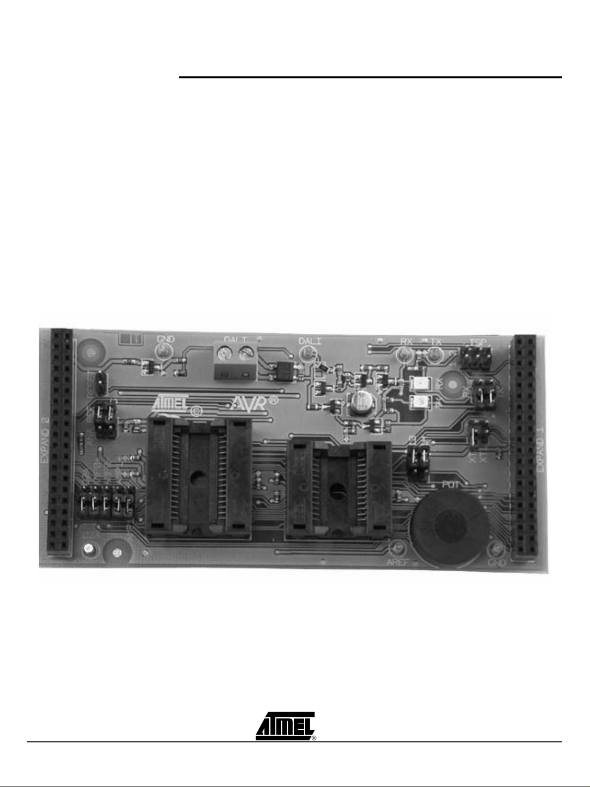
The STK520 board is a top module de signed to ad d AT90PW M family suppo rt to the
STK500 development board from Atmel Corporation.
The STK520 includes connectors and hardware allowing full utilization of the new features of th e AT90 PWM , whil e th e Ze ro I nser tio n For ce (Z IF) soc ket allo ws eas y t o use of
SO24 & SO32 packages for prototyping.
This user guide ac ts as a gen eral ge tting st arted gui de as wel l as a compl ete tec hnical
reference for advanced users.
Notice that in this guide, the word AVR is used to refer to the target component
(AT90PWM2, AT90PWM3...)
Figure 1-1. STK520 Top Module for STK500
Introduction
Section 1
Introduction
STK520 User Guide 1-2
7510A–AVR–08/05
Page 4

Introduction
1.1 Features STK520 is a New Member of the Successful STK500 Starter Kit Family.
Supports the AT90PWM2 & AT90PWM3.
DALI Hardware Interface.
®
Supported by AVR Studio
Zero Insertion Force Socket for SO24 & SO32 Packages.
High Voltage Parallell Programming.
Serial Programming.
DALI Peripherals can be Disconnected from the Device.
6 Pin Connector for On-chip Debugging using JTAG MKII Emulator.
Potentiometer for the Demo Application.
Quick Reference to all Switches and Jumpers in the Silk-Screen of the PCB.
4.
1-3 STK520 User Guide
7510A–AVR–08/05
Page 5
Using the STK520 Top Module
Section 2
Using the STK520 Top Module
2.1 Connecting the STK520 to the STK500 Starter Kit
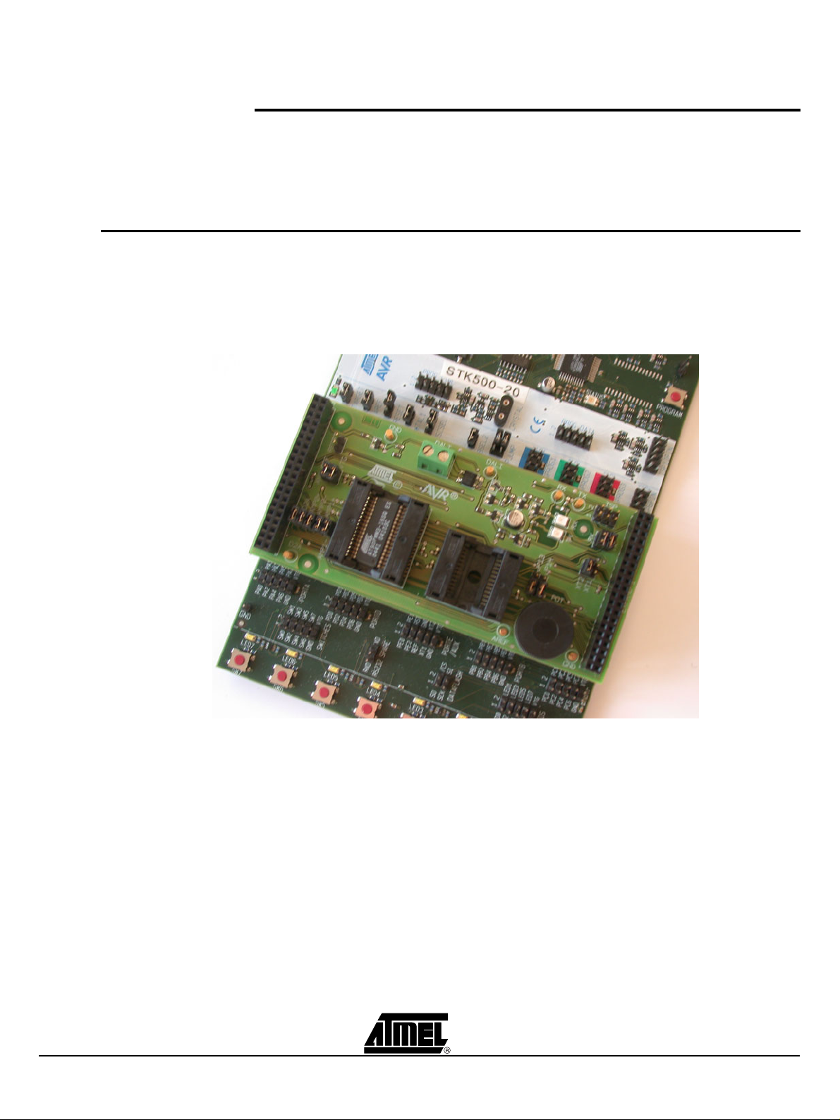
Figure 2-1. Connecting STK520 to the STK500 Board
Connect the STK520 to the STK500 expansion header 0 and 1. It is important that the
top module is connected in the correct orienta tion as show n in Figure 2-1 . The
EXPAND0 written on the STK520 top module should match the EXPAND0 written
beside the expansion header on the STK500 board.
Note: Connecting the STK520 with wrong orientation may damage the board.
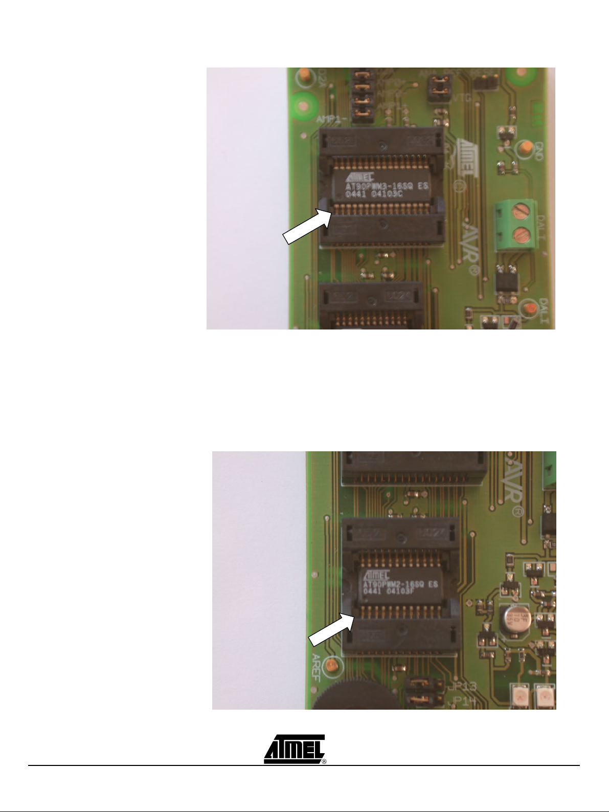
2.1.1 Placing an AT90PWM3 on the STK520
STK520 User Guide 2-4
The STK520 contains both a ZIF socket for a SO32 package. Care should be taken so
that the device is moun ted with the corr ect ori entatio n. Figur e 2-2 sh ows the l ocation o f
pin1 for the ZIF socket.
7510A–AVR–08/05
Page 6
Using the STK520 Top Module
Figure 2-2. Pin1 on ZIF Socket
PIN1
2.1.2 Placing an AT90PWM2 on the STK520
Caution: Do not mount an AT90PWM3 on the STK520 at the same time as an AVR is
mounted on the STK500 board or at the same time as an AT90PWM2 is mounted on the
STK520 board. None of the devices might work as intended.
The STK520 contains both a ZIF socket for a SO24 package. Care should be taken so
that the device is moun ted with the corr ect ori entatio n. Figur e 2-2 sh ows the l ocation o f
pin1 for the ZIF socket.
Figure 2-3. Pin1 on ZIF Socket
PIN1
2-5 STK520 User Guide
7510A–AVR–08/05
Page 7

Using the STK520 Top Module
Caution: Do not mount an AT90PWM2 on the STK520 at the same time as an AVR is
mounted on the STK500 board or at the same time as an AT90PWM3 is mounted on the
STK520 board. None of the devices might work as intended.
STK520 User Guide 2-6
7510A–AVR–08/05
Page 8
Using the STK520 Top Module
2.2 Programming the AVR
2.2.1 In-System Programming
The AVR (AT90PWM2, AT90PWM3...) can be programmed using both SPI and Highvoltage Parallel Programming. This section will explain how to connect the programming
cables to successfully use one of these two modes. The AVR Studio STK500 software
is used in the same way as for other AVR parts
Note: The AT90PWM3 also support Self Programming, See AVR109 application note
for more information on this topic.
Figure 2-4. In-System Programming
To program the AT 90PWM3 us ing ISP Programm ing mode , connect t he 6-wire cable
between the ISP 6PIN connec tor on the STK500 boar d and the ISP connector o n the
STK520 board as shown in Figure 2-4. The device can be programmed using the Serial
Programming mode in the AVR Studio4 STK500 software.
Note: See STK500 User Guide for information on how to use the STK500 front-end
software for ISP Programming.
2-7 STK520 User Guide
7510A–AVR–08/05
Page 9

Using the STK520 Top Module
2.2.2 High-voltage Programming
Figure 2-5. High-voltage (Parallel) Programming
To program the AVR u sing High -voltag e (Parall el) Progr amming , connect the PROGCTRL to PORTD and PROGDATA to PORTB on the STK500 as shown in Figure 2-5.
Make sure that the TOSC-switch is placed in the XTAL position.
As described in the STK500 User Gu ide (jump er setti ngs), mount the BS EL2 jum per in
order to High-voltage Program the ATmega devices. This setting also applies to Highvoltage Programming of the AVR.
The device can now be programmed using the High-voltage Programming mode in AVR
Studio STK500 software.
Note: See the STK500 User Guide for information on how to use the STK500 front-
end software in High-voltage Programming mode.
Note: For the High-voltage Programming mode to function correctly, the target voltage
must be higher than 4.5V.
STK520 User Guide 2-8
7510A–AVR–08/05
Page 10

Using the STK520 Top Module
2.3 JTAGICE mkII Connector
See the following document :
“JTAGICE mkII Quick Sta rt Guide” wh ich purpos e is “Connec ting to a target bo ard with
the AVR JTAGICE mkII”.
This note explains whi ch signals are required for IS P and which si gna ls are r eq uir ed for
debugWIRE.
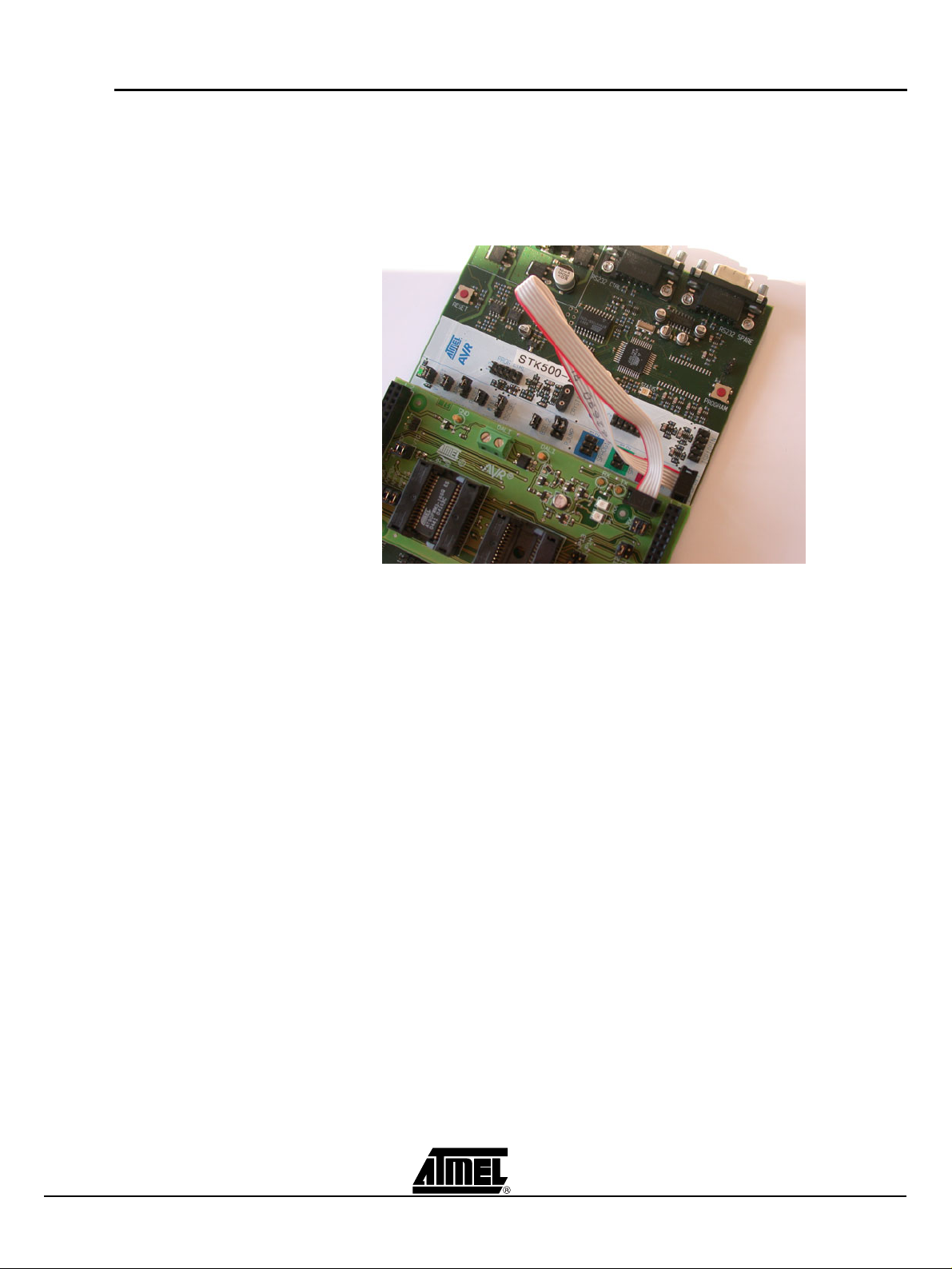
Figure 2-6 shows how to connect the JTAGICE mkII probe on the STK520 board.
Figure 2-6. Connecting JTAG ICE to the STK520
The ISP connector is used for the AT90PWM 3 built- in debu gWire int erfac e. The pin out
of the connector is shown in Table 2-1 and is compliant with the pin out of the JTAG ICE
available from Atmel . Connectin g a JTAG ICE to this connec tor allows On -chip Debu gging of the AT90PWM3.
More information about the JTAG ICE and On-chip Debugging can be found in the AVR
JTAG ICE User Guide, which is available at the Atmel web site, www.atmel.com.
2-9 STK520 User Guide
7510A–AVR–08/05
Page 11

Figure 2-7. JTAG Connector
Using the STK520 Top Module
Table 2-1. STK520 ISP Connector Pinout
Squid
Cable
Colours
grey MISO 1 2 VTG purple
black SCK 3 4 MOSI red
green RESET 5 6 GND brown
Target
pins STK520 ISP pinout
Target
pins
Squid
Cable
Colours
STK520 User Guide 2-10
7510A–AVR–08/05
Page 12

Using the STK520 Top Module
2.4 STK520 Jumpers, Leds & Test Points
Table 2-2. STK520 Jumpers
Jumper Function Description
JP1 XT1 Connect STK500 XT1 circuit to AVR PE1
JP2 XT2 Connect STK500 XT2 circuit to AVR PE2
JP3 RESET Connect STK500 RESET circuit to AVR PE0
JP4 RX Connect RxD DALI to RxD Input of the AVR
JP5 TX Connect TxD DALI to TxD Output of the AVR
JP6 VTG Useful to measure the VCC and AVCC current
JP7 ANA REF Connect STK500 REF circuit to AVR AREF
JP8 D2A Isolate D2A outpu
JP9 AMP0+ Isolate AMP0+ input
JP10 AMP0- Isolate AMP0- input
JP11 AMP1+ Isolate AMP1+ input
JP12 AMP1- Isolate AMP1- input
JP13 Potentiometer supply from Analog V Ref
JP14 Potentiometer output to ADC0 input
Table 2-3. STK520 Leds
Led Function Description
D3 RX RX data detected by DALI Interface
D4 TX TX data sent to DALI Interface
Table 2-4. STK520 Test Points
Test Point Function Description
T1 GND Electrical ground of the STK520 board
T2 GND Electrical ground of the STK520 board
T3 AREF AREF pin of the AVR
T4 D2A D2A output of the A V R
T5 DALI Rectified DALI line
T6 Tx TX data sent to DALI Interface
T7 Rx RX data detected by DALI Interface
2-11 STK520 User Guide
7510A–AVR–08/05
Page 13

Using the STK520 Top Module
e
2.5 DALI Interface STK520 includes a non-isolated DALI Interface. The DALI Interface converts AVR RxD
and TxD pin level to DALI compatible electri cal level. It acts as a duplexer, so it inter faces the two RxD and TxD lines to one DALI line.
To use the DALI Interface, it is neces sary to mount T xD and RxD jumpers. W hen these
jumpers are removed, the AVR is not inflenced by the interface. The TxD and RxD AVR
pins are also available on STK500 PD3 and PD4 connectors.
Thanks to a diode bridge, the DALI connector is not polarized.
Figure 2-8. DALI
DALI Transmitter
DALI Receiver
Bridge
Rectifier
J3
DALI Lin
AVR
TxD
RxD
PD4 PD3
JP5
JP4
TX Led &
Test Point
RX Led &
Test Point
Figure 2-9. DALI Connector
STK520 User Guide 2-12
7510A–AVR–08/05
Page 14

Using the STK520 Top Module
2.6 Potentiometer The STK520 includes a potentiometer. To use the potentiom eter, please mo unt JP13
and JP14 jumper.
The potentiometer is supplied by AREF and it delivers a voltage to the AVR ADC0 input.
Figure 2-10. Potentiometerr
2.6.0.1 XT1 Jumper As the jumper JP1 (XT1) is short circuited by Printed Circuit Board wire, it’s always ON.
So it’s not mounted. To open this jumper, it’s necessary to cut the wire between JP1 pin
(solder side).
It’s possible to open XT AL1 circui t which comes from STK500 board by removing the
XTAL1 jumper on the STK500 board.
2.6.0.2 RESET Jumper As the jumper JP3 (R ESET ) is sh ort cir cuite d by Pri nted Circui t Board wire , it’s al ways
ON. So it’s not mounted. To open this jumper, it’s necessary to cut the wire between
JP3 pin (solder side).
It’s possible to open RESET circuit which comes from STK500 board by removing the
RESET jumper on the STK500 board.
2-13 STK520 User Guide
7510A–AVR–08/05
Page 15

Troubleshooting Guide
Table 3-1. Troubleshooting Guide
Problem Reason Solution
ISP cable not connected. Connect the ISP cable according to
Figure 2-4.
Serial Programming
does not work
STK500 target voltage
error.
Please refer to the AT90PWM3
datasheet for the Serial
Programming Voltage limits. Adjust
the target voltage on the STK500
board accordingly.
Section 3
The RSTDISBL Fuse is
programmed.
Cables not connected
properly.
Parallel Programming
does not work.
Emulation does not
work.
Note: 1. See the application note “AVR065: LCD Driver for the STK520 LCD” on how to con-
trol the LCD-display or the the application note “AVR064: STK520 – A Temperature
Monitoring System with LCD Output”.
STK500 target voltage
error.
ISP cable not connected. Connect the ISP cable according to
Conflict with STK500
Reset
DWEN fuse is not
programmed
The RSTDISBL Fuse is
programmed.
Use Parallel Programming to
unprogram the RSTDISBL Fuse.
Please refer to Figure 2-5 for
correct Parallel Programmi ng set up.
Please refer to the AT90PWM3 data
sheet for the Parallel Programming
Voltage limits. Adjust the target
voltage on the STK500 board
accordingly.
Figure 2-7.
Remove Reset Jumper on STK500
Board
Please set the DWEN bit using
parallel programming
Use Parallel Programming to
unprogram the RSTDISBL Fuse.
STK520 User Guide 3-14
Rev. 7510A–AVR–08/05
Page 16

Technical Specifications
Section 4
Technical Specifications
System Unit
Physical Dimensions . . . . . . . . . . . . . . . . . . . . . . . . . . . . . . . . . . . . . . 56 x 119 x 27 mm
Weight . . . . . . . . . . . . . . . . . . . . . . . . . . . . . . . . . . . . . . . . . . . . . . . . . . . . . . . . . . . . 70 g
Operating Conditions
Voltage Supply . . . . . . . . . . . . . . . . . . . . . . . . . . . . . . . . . . . . . . . . . . . . . . . .1,8V - 5,5V
Temperature . . . . . . . . . . . . . . . . . . . . . . . . . . . . . . . . . . . . . . . . . . . . . . . . . . 0°C - 50°C
DALI Interface
Maximum DALI Voltage. . . . . . . . . . . . . . . . . . . . . . . . . . . . . . . . . . . . . . . . . . . . . . . 25V
Maximum Input DALI Current . . . . . . . . . . . . . . . . . . . . . . . . . . . . . . . . . . . . . . . . 500mA
STK520 User Guide 4-16
7510A–AVR–08/05
Page 17

Technical Support
Section 5
Technical Support
For Technical supp ort, pleas e cont act av r@atmel. co m. When requesti ng te chnica l support, please include the following information:
Which target AVR device is used (complete part number).
Target voltage and speed.
Clock source and fuse setting of the AVR.
Programming method (ISP or High-voltage).
Hardware revisions of the AVR tools, found on the PCB.
Version number of AVR Studio. This can be found in the AVR Studio help menu.
PC operating system and version/build.
PC processor type and speed.
A detailed description of the problem.
STK520 User Guide 5-18
7510A–AVR–08/05
Page 18

Section 6
Complete Schematics
On the following pages the co mplete sch ematics an d assembly dr awing of the ST K520
revision A are shown.
STK520 User Guide 6-18
Rev. 7510A–AVR–08/05
Page 19

Complete Schematics
Figure 6-1. Schematics, 1 of 4
1
R12KR1
2
C2
1nFC21nF
AREFT
PE[2..0]
PD[7..0]
PC[7..0]
PB[7..0]
of
of
of
1
14Wednesday, November 10, 2004
14Wednesday, November 10, 2004
14Wednesday, November 10, 2004
2K
Q1
BC847BQ1BC847B
PB[7..0]
PC[7..0]
PD[7..0]
PE[2..0]
R2
10KR210K
C3
100nFC3100nF
REF
PE0
PC4
PC0
PC6
PE2
VTGVTGVTGVTG
4
6
8
10
2
12
16
18
14
PC2
22
24
26
28
20
PE2
30
40
32
34
36
38
STK520 MEZZANINE FOR STK500
Title
Title
Title
POWER & EXPENSION CONNECTORS
POWER & EXPENSION CONNECTORS
POWER & EXPENSION CONNECTORS
Size Document Number Rev
Size Document Number Rev
Size Document Number Rev
2
<Doc> 1.6.0
<Doc> 1.6.0
<Doc> 1.6.0
A
A
A
Date: Sheet
Date: Sheet
Date: Sheet
PE2
CT6
CT4
GND
AUXO0
JP2
JP2
1 2
PE2
PE0
J2
J2
GND
AUXI0
CT7
CT5
1
3
5
7
XT2
XT2
JP3
JP3
1 2
CP2CP2
RESET
RESET
PE1
3
PE0
CT2
REF
VTG
GND
BSEL2
CT3
CT1
(n.c.)
NRST
PE1
GND
VTG
9
11
13
15
17
19
21
PC7
PE1
PA6
PA4
PA2
PC6
PC4
PC2
PC7
PC5
PC3
23
25
27
PC3
PC5
PC1
PA0
PC0
PC1
29
31
PA7
33
PA5
35
PA3
GND
CON 2x20
CON 2x20
EXP. CON 0
GND
39
EXP. CON 0
3
PA1
37
RESET
PB6
PB0
PB4
PB2
JP1
JP1
4
5
CP1CP1
XT1
XT1
1 2
4
2
6
8
GND
DATA6
DATA4
AUXO1
J1
J1
GND
AUXI1
DATA7
DATA5
1
3
5
7
100nFC1100nF
18
14
10
12
SO
DATA0
DATA9
DATA3
DATA1
SI
9
11
13
C1
24
26
20
16
22
CS
XT2
PB6
VTG
GND
SCK
XT1
VTG
GND
PB7
15
17
19
21
23
25
XT1 XT2
PB5
PB7
PB4
PB5
PB3
28
27
PB2
PB3
PB1
30
29
PD4
PB0
PB1
PD7
PD2
PD6
PD0
32
34
36
38
40
PD6
PD4
PD2
PD0
GND
CON 2x20
CON 2x20
EXP. CON 1
GND
39
EXP. CON 1
PD7
PD5
PD3
PD1
31
33
35
37
PD1
PD3
PD5
4
PA0 is connected to PE2 for BSEL2 function.
5
Note : JP1 and JP3 are not mounted
D D
C C
B B
A A
6-19 STK520 User Guide
7510A–AVR–08/05
Page 20

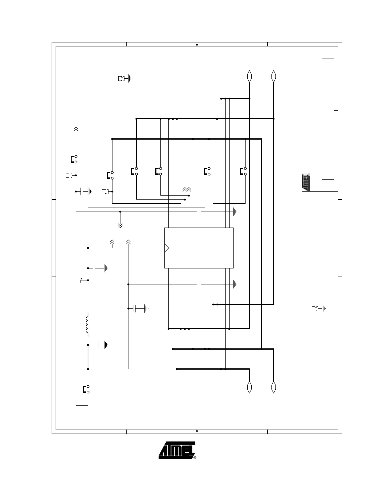
Figure 6-2. Schematics, 2 of 4
1
PD[7..0]
Complete Schematics
of
of
of
1
24Wednesday, November 10, 2004
24Wednesday, November 10, 2004
24Wednesday, November 10, 2004
VTG
R3 1K5R3 1K5
R4 1K5R4 1K5
RxD DALI
RxD DALI
D4
REDD4RED
JP4
D3
GREEND3GREEN
2
TP
T7
TP
T7
Rx
Rx
TP
T6
TP
T6
Tx
Tx
VTG
C4
10µF+C4
3
10µF
+
JP4
R6
10KR610K
23
C5
1nFC51nF
R5
2K2R52K2
PD4PD4
1 2
R9
BC857BQ2BC857B
1
PD3
TxD DALI
TxD DALI
JP5
JP5
1 2
STK520 MEZZANINE FOR STK500
ISP, MONCOM, DALI
ISP, MONCOM, DALI
ISP, MONCOM, DALI
Title
Title
Title
Q3
BC847BQ3BC847B
10KR910K
Q2
10KR810K
R8
VTG
R11
R11
100K
100K
R12
10K
R12
10K
1
23
VTG
Q4
BC857BQ4BC857B
R14
R14
10K
10K
C6
100nFC6100nF
VTG
2
6
4
PDI
VCC
GND
Size Document Number Rev
Size Document Number Rev
Size Document Number Rev
2
<Doc> 1.6.0
<Doc> 1.6.0
<Doc> 1.6.0
A
A
A
Date: Sheet
Date: Sheet
Date: Sheet
3
ISP CON
J4
4
D1
BAS16D1BAS16
1 2
TP
T5
TP
T5
DALI
DALI
BR1
BR1
1
R7
10KR710K
4
MB2S
MB2S
3
-+
-+
R15
R15
10K
10K
R10
R10
10R
10R
R131KR13
1K
Q5
FMMT491AQ5FMMT491A
J4
PDO
1
PD4
PD2
PD3
ISP CON
CON 2x3
CON 2x3
SCK
RESET
5
3
PE0
4
2
5
DALI INTERFACE
1
2
J3
D D
DALIJ3DALI
C C
B B
PD[7..0]
PE[2..0]
A A
5
STK520 User Guide 6-20
7510A–AVR–08/05
Page 21
Complete Schematics
Figure 6-3. Schematics, 3 of 4
1
of
of
TP
T1
TP
T1
GND
GND
PD[7..0]
PD7
PD6
PD5PD4
PB[7..0]
of
1
34Wednesday, November 10, 2004
34Wednesday, November 10, 2004
34Wednesday, November 10, 2004
AREFT
PC7
2
JP7
JP7
ANA REF
ANA REF
1 2
TP
T3
TP
T3
C7
AREF
AREF
3
10nFC710nF
D2A
D2A
JP8
JP8
1 2
TP
T4
TP
T4
D2A
D2A
AVTG
AMP0+
AMP0+
JP9
JP9
VTG_SO
PB4
PB3
PB5
PB6
PB7
PC6
AMP0-
AMP0-
JP10
JP10
1 2
1 2
PB4_SO
PB3_SO
25
28
32
26
29
PB327PB4
PB530PB631PB7
PC6
PC7
AREF_SO
100nF
100nF
C10
C10
U101
U101
PD01PC02PE03PD14PD25PD36PC17VCC8GND9PC210PC311PB012PB113PE114PE215PD4
AREF
AMP1+
AMP1+
JP11
JP11
24
AGND
PB2
PC5
1 2
23
20
19
22
PB2
PC421PC5
AVCC
PC4
Size Document Number Rev
Size Document Number Rev
Size Document Number Rev
2
<Doc> 1.6.0
<Doc> 1.6.0
<Doc> 1.6.0
A
A
A
Date: Sheet
Date: Sheet
Date: Sheet
3
AMP1-
AMP1-
JP12
JP12
1 2
STK520 MEZZANINE FOR STK500
Title
Title
Title
MICROCONTROLLER 32 PIN SOCKET
MICROCONTROLLER 32 PIN SOCKET
MICROCONTROLLER 32 PIN SOCKET
PD517PD618PD7
SOIC32
SOIC32
32 Pin Socket
32 Pin Socket
16
AVTG
PB0
PB1
TP
T2
TP
4
L1
L1
BLM-21A102S
BLM-21A102S
C8
100nFC8100nF
C11
C11
100nF
100nF
PD3
PD2
PD0
PD1
PC3
PC2
PE0
PC1
PE2
PE1
PC0
T2
GND
GND
4
PE[2..0]
5
JP6
JP6
VTG
VTG
1 2
VTG
D D
C C
PE[2..0] PD[7..0]
B B
PC[7..0]
5
PC[7..0] PB[7..0]
A A
6-21 STK520 User Guide
7510A–AVR–08/05
Page 22

Figure 6-4. Schematics, 4 of 4
1
PB7
PB6
PB5
PB2PB1
Complete Schematics
PB[7..0]
of
of
of
1
44Wednesday, November 10, 2004
44Wednesday, November 10, 2004
PD[7..0]
PD7
PD5PD4
PD6PE2
PB[7..0]
44Wednesday, November 10, 2004
2
2
STK520 MEZZANINE FOR STK500
<Doc> 1.6.0
MICROCONTROLLER 24 PIN SOCKET
<Doc> 1.6.0
MICROCONTROLLER 24 PIN SOCKET
<Doc> 1.6.0
MICROCONTROLLER 24 PIN SOCKET
A
A
A
Title
Size Document Number Rev
Size Document Number Rev
Size Document Number Rev
Date: Sheet
Date: Sheet
Date: Sheet
3
4
PB3_SO
PB4_SO
19
24
C12
100nF
C12
3
100nF
100nF
100nF
C13
C13
U102
U102
AVTG
PD01PE02PD13PD24PD35VCC6GND7PB08PB19PE110PE211PD4
16
17
18
15
PB2
PB320PB421PB522PB623PB7
AREF
AGND
PD513PD614PD7
AVCC
SOIC24
SOIC24
24 Pin Socket
24 Pin Socket
Title
Title
12
C14
C14
100nF
4
100nF
PD1
PD0
PB0
PD3
PD2
VTG_SO
JP14JP14
1 2
JP13JP13
PE0
P1
100KP1100K
PE1
PE[2..0]
1 2
5
5
PE[2..0] PD[7..0]
AREF_SO
D D
C C
B B
A A
STK520 User Guide 6-22
7510A–AVR–08/05
Page 23

Complete Schematics
Figure 6-5. Assembly Drawing, 1 of 1
JUMPER
6-23 STK520 User Guide
7510A–AVR–08/05
Page 24

Atmel Headquarte rs Atmel Operations
Corporate Headquarters
2325 Orchard Parkway
San Jose, CA 95131
TEL 1(408) 441-0311
FAX 1(408) 487-2600
Europe
Atmel Sarl
Route des Arsenaux 41
Case Postale 80
CH-1705 Fribourg
Switzerland
TEL (41) 26-426-5555
FAX (41) 26-426-5500
Asia
Room 1219
Chinachem Gol den P laza
77 Mody Road Tsimhatsui
East Kowloon
Hong Kong
TEL (852) 2721-9778
FAX (852) 2722-1369
Japan
9F, Tonetsu Shinkawa Bldg.
1-24-8 Shin kawa
Chuo-ku, Tokyo 104-0033
Japan
TEL (81) 3- 3523-3 551
FAX (81) 3-3523-7581
Memory
2325 Orchard Parkway
San Jose, CA 95131
TEL 1(408) 441-0311
FAX 1(408) 436-4314
Microcontrollers
2325 Orchard Parkway
San Jose, CA 95131
TEL 1(408) 441-0311
FAX 1(408) 436-4314
La Chantrerie
BP 70602
44306 Nantes Cedex 3, France
TEL (33) 2-40-18-18-18
FAX (33) 2- 40-18- 19-6 0
ASIC/ASSP/Smart Cards
Zone Industrielle
13106 Rousset Cedex, France
TEL (33) 4-42-53-60-00
FAX (33) 4- 42-53- 60-0 1
1150 East Cheyenne Mtn. Blvd.
Colorado Springs, CO 80906
TEL 1(719) 576-3300
FAX 1(719) 540-1759
Scottish Enterprise Technology Park
Maxwell Building
East Kilbride G75 0QR, Scotland
TEL (44) 1355-803-000
FAX (44) 1355-242-743
RF/Automotive
Theresienstrasse 2
Postfach 3535
74025 Heilbro nn, Ge rmany
TEL (49) 71-31-67-0
FAX (49) 71-31-67-2340
1150 East Cheyenne Mtn. Blvd.
Colorado Springs, CO 80906
TEL 1(719) 576-3300
FAX 1(719) 540-1759
Biometrics/Imaging/Hi-Rel MPU/
High Speed Converters/RF Datacom
Avenue de Rochepleine
BP 123
38521 Saint-Egreve Cedex, France
TEL (33) 4-76-58-30-00
FAX (33) 4- 76-58- 34-8 0
e-mail
literature@atmel.com
Web Site
http://www.atmel.com
Disclaimer: The information in this document is provided in connection w ith A tmel prod ucts. No license, express or im plied, by estoppel or otherwi se,to anyintel lectualproperty right is granted by this document or in connection with the sale of A tmel products. EXCEPT AS SET FORTH IN ATMEL’S TERMS AND CONDI-TIONS OF
SALE LOCATED ON ATMEL’S WEB SITE, ATMEL ASSUMES NO LIAB ILITY WHATSOEVER AND DISCLAIMS ANY EXPRESS, IMPLIED OR STATUTORYWARRANTY RELATING TO ITS PRODUCTS INCLUDING, BUT NOT LIMITED TO, THE IMPLIED WARRANTY OF MERCHANTABILITY, FITNESS FOR A PARTICULARPURPOSE, OR NON-INFRINGEMENT. IN NO EVENT SHALL ATMEL BE LIABLE FOR ANY DIRECT, INDIRECT, CONSEQUENTIAL, PUNITIVE, SPECIAL
OR INCIDEN-TAL DAMAGES (INCLUDING, WITHOUT LIMITATION, DAMAGES FOR LOSS OF PROFITS, BUSINESS INTERRUPTION, OR LOSS OF INFORMATION) ARISING OUTOF THE USE OR INABILITY TO USE THIS DOCUMENT, EVEN IF ATMEL HAS BEEN ADVISED OF THE POSSIBILITY OF SUCH DAMAGES. Atmel makes norepresentationsor warranties with respect to the accuracy or completeness of the contents of this document and reserves the ri ght to make
changes to specificationsand product descriptions at any time without notice. Atmel does not make any commitment to update the informati on contained herein.
Unless specifically provided otherwise, Atmel products are not suitable for, and sh all not be used in, automotive applications. Atmel’s products are not i ntended,
authorized, or warranted for useas components in applications intended to support or sustainlife.
© Atmel Corporation 2005. All righ ts reserved. Atmel®, logo and combinations thereof, are registered trademarks, and Ev erywhere You Are
are the trademarks of Atmel Corporation or its subsidiaries. Other terms and product names may be trademarks of others.
Printed on recycled paper.
7510A–AVR–08/05
SM
/0M
 Loading...