

Page 1

STK511
....................................................................................................................
AVR-based Uni-directional
Radio Starter Kit
User Guide
4842B–AVR–10/09
Page 2

Table of Contents
Section 1
Overview .................................................................................................................... 1-1
1.1 Features............................................................................................................................. 1-1
1.2 Introduction ........................................................................................................................ 1-1
Section 2
Getting Started ........................................................................................................... 2-1
2.1 Setting up the Hardware .................................................................................................... 2-1
2.2 Configuring the Receiver ................................................................................................... 2-1
2.3 Running the Demo .............................................................................................................2-2
2.3.1 STK500 Configuration ......................................................................................... 2-2
2.3.2 STK511 Receiver Interface Board Configuration................................................. 2-3
2.3.3 Using the Transmitter .......................................................................................... 2-3
2.4 Evaluating the Demo..........................................................................................................2-3
Section 3
STK511 Receiver Board............................................................................................. 3-1
3.1 Hardware Description ........................................................................................................ 3-1
3.1.1 Overview.............................................................................................................. 3-1
3.1.2 IC_Active LED ..................................................................................................... 3-1
3.1.3 CDEM Capacitor.................................................................................................. 3-1
3.1.4 Mode Selection.................................................................................................... 3-1
3.1.5 XTAL Oscillator.................................................................................................... 3-2
3.1.6 Signal Testpoints ................................................................................................. 3-2
3.1.7 Antenna Matching................................................................................................ 3-2
3.2 Software Description.......................................................................................................... 3-3
3.2.1 Overview.............................................................................................................. 3-3
3.2.2 Sample Software ................................................................................................. 3-3
Section 4
STK511 Receiver Interface Board..............................................................................4-1
4.1 Hardware Description ........................................................................................................ 4-1
4.1.1 Standalone Configuration .................................................................................... 4-2
4.1.2 STK500/511 Assembly Configuration.................................................................. 4-3
4.2 STK511 RF Receiver Interface Board ............................................................................... 4-3
4.2.1 Receiver Connectors ........................................................................................... 4-3
4.2.2 Configuration Register DIP Switches................................................................... 4-4
STK511 User Guide i
4842B–AVR–10/09
Page 3

Table of Contents (Continued)
4.3 Software Description.......................................................................................................... 4-6
Section 5
STK511 Transmitter Board.........................................................................................5-1
5.1 Hardware Description ........................................................................................................ 5-1
5.2 Software Description.......................................................................................................... 5-5
4.2.3 Configuration Register LED Indicators ................................................................ 4-5
4.2.4 DATA Selector Switch ......................................................................................... 4-5
4.2.5 Configure Push Button ........................................................................................ 4-5
4.2.6 On-board Microcontroller ..................................................................................... 4-5
4.2.7 Receive Signal Routing ....................................................................................... 4-6
4.3.1 Overview.............................................................................................................. 4-6
4.3.2 Sample Software ................................................................................................. 4-7
5.1.1 Overview.............................................................................................................. 5-1
5.1.2 Physical Features ................................................................................................ 5-1
5.1.3 Functional Features ............................................................................................. 5-2
5.1.4 Circuit Description................................................................................................ 5-3
5.2.1 Overview.............................................................................................................. 5-5
5.2.2 Sample Software ................................................................................................. 5-5
Section 6
Regulatory Requirements...........................................................................................6-1
6.1 General .............................................................................................................................. 6-1
6.2 Output Field Strength/Power.............................................................................................. 6-1
6.3 Operating Frequency ......................................................................................................... 6-2
6.4 Operating Duty Cycle.........................................................................................................6-2
6.5 Additional information ........................................................................................................ 6-2
Section 7
Troubleshooting Guide...............................................................................................7-1
ii STK511 User Guide
4842B–AVR–10/09
Page 4

1.1 Features
Plug-in Connectors Accept ATA5743/44/60/61 RF Receiver Application Board
DIP Switches Define Configuration Register Settings
LED Indicators Provide Programming Status of Configuration Register
Data Selector Switch Enables Fast Transition Between Operating Modes
Configuration Programming Button Simplifies Programming
Fully Compatible STK
1.2 Introduction
This document explains the operation of the STK511 – an AVR®-based UHF Radio Evaluation Kit. The
STK511 Starter Kit was developed as a tool for evaluating Atmel's receivers (ATA5743, ATA5744,
ATA5760 and ATA5761) and transmitters (T5750, T5753 and T5754). Although most Atmel receivers
require programming of configuration registers via a bi-directional, one-wire interface, this kit provides
register programming in an easy to use way for the customer to quickly evaluate an AVR-based UHF
Radio system. Included in this kit is software to evaluate both ASK and FSK modulated radio systems
across the RF spectrum of 315
transmitters. While above mentioned ICs are supported by this kit, pre-configured kits are only available
for 868
®
500 Interface Connectors
MHz to 915 MHz and complete reference designs for receivers and
MHz (using ATA5760 and T5750) and 915 MHz (with ATA5761 and T5750).
Section 1
Overview
In addition to providing a quick, one-step, programming tool for configuring Atmel RF receivers, the
Receiver Interface Board of the STK511 Starter Kit doubles as an expansion card for the STK500. This
allows the user to develop software for receiver applications using any of the AVR microcontrollers sup
ported by the STK500. The STK511 Starter Kit, when combined with the STK500, enables extremely
quick prototype development for customers interested in Atmel's UHF radio design solutions.
STK511 User Guide 1-1
4842B–AVR–10/09
-
Page 5
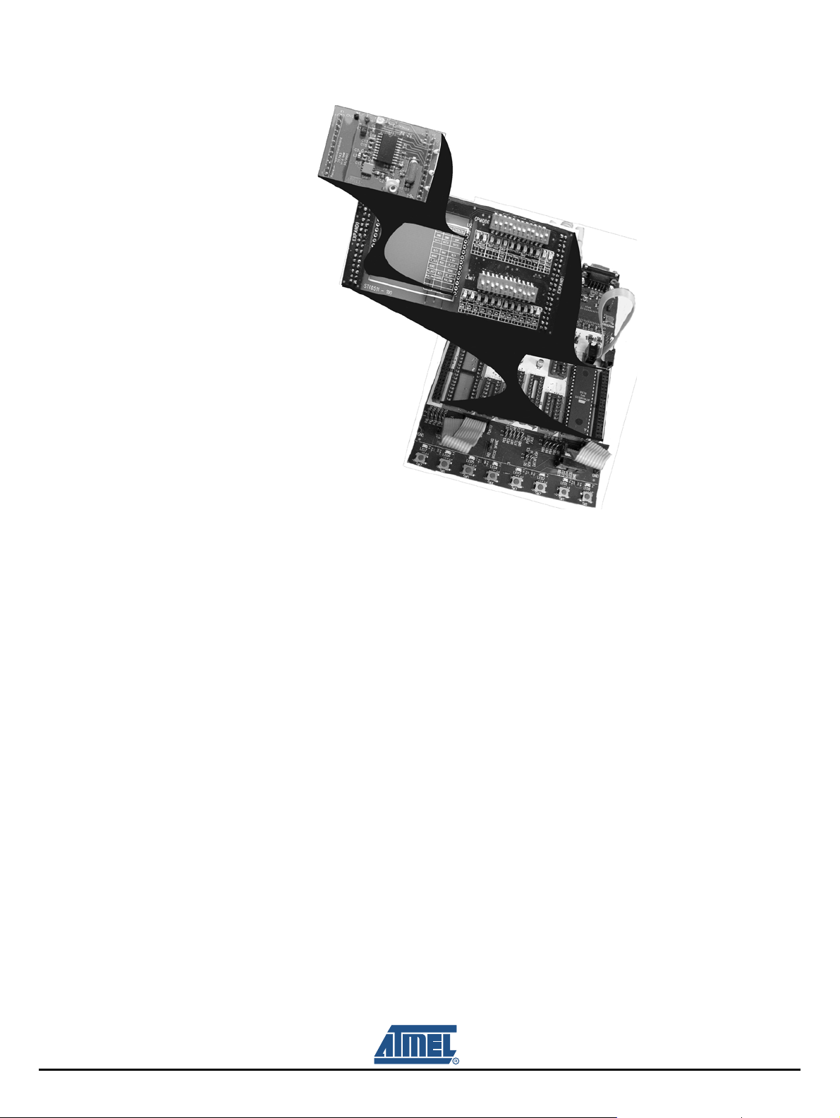
Overview
Figure 1-1. STK511 Starter Kit
Included in the Kit:
STK511 Receiver Interface Board
RF Receiver Application Board (one of the following)
– ATA5760 (868 MHz)
– ATA5761 (915 MHz)
RF Transmitter Application Board
– Tiny13 + T5750 (868/915 MHz)
CD containing sample software
One CR2032 battery
External whip antenna (RX only, TX antenna is PCB trace)
Optional items not included in the kit:
Atmel AVR STK500 Starter Kit and Development System
1-2 STK511 User Guide
4842B–AVR–10/09
Page 6

The STK®511 Starter Kit comes complete with all the hardware needed to demonstrate a working RF
system. Included are the STK511Interface Board, RF Receiver Application Board, and RF Transmitter
Application Board.
2.1 Setting up the Hardware
The Receiver Application Board should be oriented with its signal pins toward the DIP switches and
LEDs on the STK511 Receiver Interface Board. This places the power and ground test points on the top
of the receiver board adjacent to the DATA selector switch. Insert the receiver board into the provided
connectors.
If the STK511 Receiver Interface Board is used as an expansion card for the STK500, align the
EXPAND0 and EXPAND1 connectors with the corresponding EXPAND0 and EXPAND1 headers on the
STK500 and press together. Be cautious of pinching any ribbon cable ends on the STK500 board when
inserting the STK511 Receiver Interface Board into the connectors.
Once the Receiver Application Board has been inserted into both twelve-pin connectors, power must be
supplied in one of two ways:
Section 2
Getting Started
A) the power and ground pins on the Receiver Application Board can be connected to a +5V supply, or
B) the supply can be sourced through the STK500 connectors EXPAND0 and EXPAND1.
If the STK500 is used to source power, the VTARGET jumper (located on the STK500) must be connected and VTARGET set to 5V in the STK500 board settings located under the appropriate tab in AVR
®
Studio
, Atmel's software development tool.
2.2 Configuring the Receiver
Atmel RF Receivers designated ATA5743, ATA5760 and ATA5761 contain two configuration registers
(Atmel RF receiver designated ATA5744 does not). These registers control the digital processing of the
incoming RF signal, as well as define the receivers’ polling interval. The register values are stored in vol
atile memory and are lost when power is removed; therefore, they must be re-programmed every time
power is applied. Programming is achieved with a one-wire protocol using the receivers’ DATA line. This
line is bi-directional and is also used for providing the demodulated data to the user. More detail on this
can be found in the individual receivers’ datasheets.
With this in mind, the user must decide how to configure the receiver for the intended application. To
illustrate this process, the following example will show how to change the receiver to ASK from its default
mode of FSK.
-
STK511 User Guide 2-1
4842B–AVR–10/09
Page 7
Getting Started
1. Once the hardware is setup, verify that the DATA selector switch is in the STK511 position.
2. Apply power, locate the DIP switch corresponding to the OPMODE register, and set the 5th DIP
switch to the ON position. The LED enclosed in the silkscreen legend labeled Mod should light up,
indicating a 1 (corresponding to ASK mode) was selected.
3. Press the Configure button to program the OPMODE and LIMIT registers with the selected
configuration.
Now, the receiver is ready to receive an ASK (or in most cases, On-Off Keyed - OOK) signal. The
demodulated signal appears on the DATA line of the Receiver Application Board. This signal can be
routed to the on-board microcontroller or to the STK500, depending on the position of the DATA selector
switch and values of jumpers R25-R32 (
information).
2.3 Running the Demo
The Transmitter Application Board contained in the evaluation kit is shipped preprogrammed with a light
intensity sensor program. It can be used with the STK500/511 Assembly to display ambient light inten
sity using LEDs on the STK500. To run this demo it must first be properly configured.
2.3.1 STK500 Configuration
1. Insert an AT90S8515 microcontroller into the red 40-pin socket (SCKT3000D3) on the STK500
board.
2. Verify that the 6-pin ribbon cable is connected between the SPROG3 and the ISP6PIN headers and
is oriented correctly.
3. Connect the 10-pin ribbon cable from the LEDS header to the PORTC header.
4. Apply power (12 V) to the supplied connector and turn on the STK500 power switch.
5. Connect the serial cable between RS232 CTRL and the host PC.
6. In AVR Studio, select Tools/STK500 from the menu.
7. Select the Board tab and verify that the VTARGET voltage is set to 5 V.
8. On the Program tab, select AT90S8515 from the Device pull-down menu.
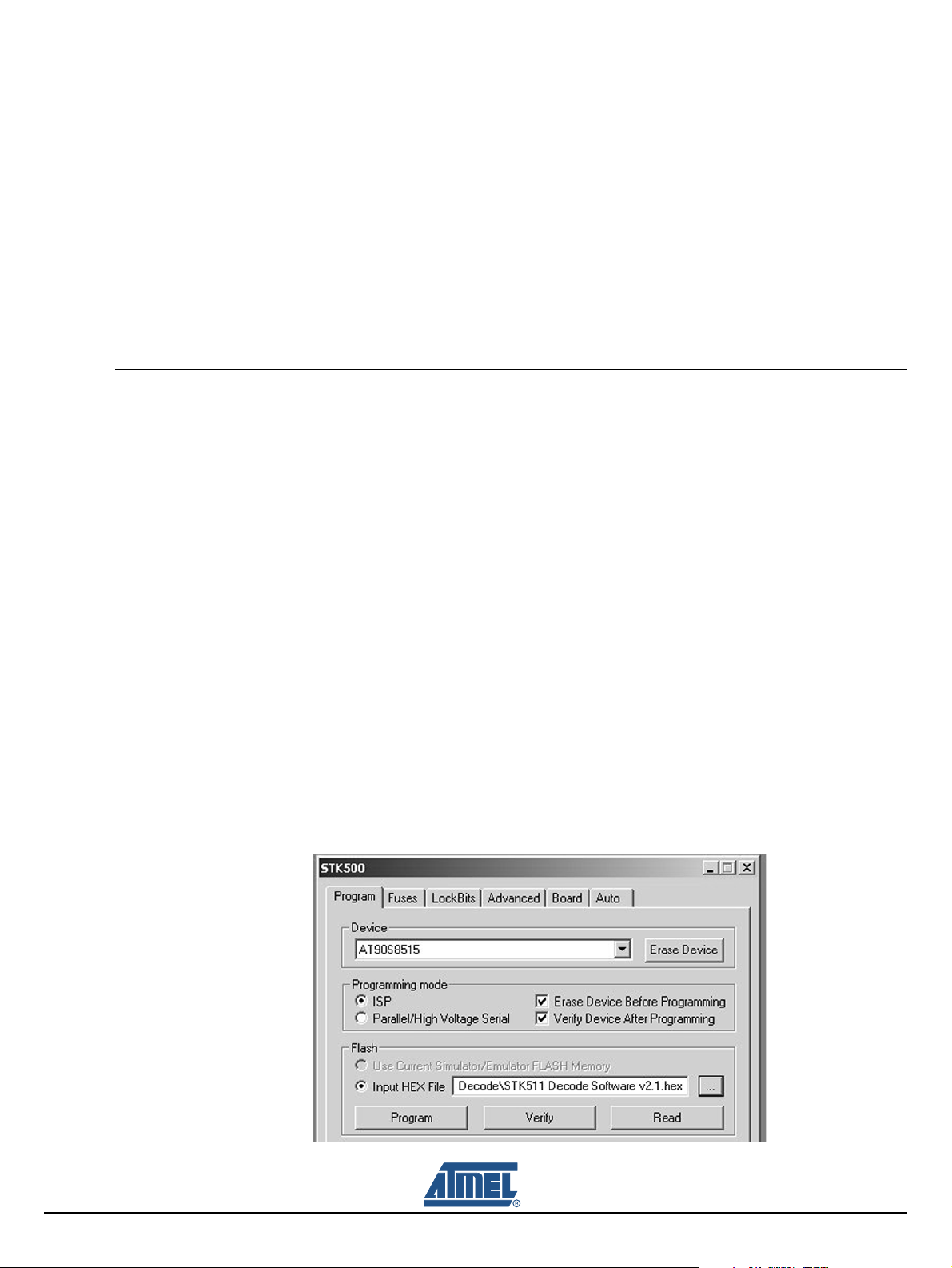
9. Load the STK511 RX Decode.hex file, included on the Sample Software CD, into the field labeled
Flash Input Hex File and press the Program button (see Figure 2-1 on page 2-2).
See “Receive Signal Routing” on page 4-6. for additional
-
Figure 2-1. Receiver Decode Software
2-2 STK511 User Guide
4842B–AVR–10/09
Page 8

2.3.2 STK511 Receiver Interface Board Configuration
1. Verify that the Receiver Application Board has been inserted into the appropriate sockets on the
STK511 Receiver Interface Board.
2. Connect the STK511 Receiver Interface Board to the STK500 by aligning EXPAND0 and EXPAND1
connectors and pressing together.
3. Switch the Data Selector switch to the STK511 position.
4. Verify power is supplied to the STK500 board.
The Transmitter Application Board as shipped will be set to run with the default receiver configuration
register settings. The DIP switches on the STK511 Receiver Interface Board should be set according to
the following values:
DIP switch #1….………..#12
OPMODE register: 000100011001
LIMIT register: 010101101001
Note: The default values are also shown on the bottom line of the silkscreen on the STK511 board.
5. Once the DIP switches have been properly set, press the Configure button to write these values into
the receiver's registers.
6. Switch the Data Selector switch to the STK500 position and the receiver is now ready to pass data
from the transmitter to the STK500 for decoding.
Getting Started
2.3.3 Using the Transmitter
To conserve battery life, the transmitter is shipped in a low current sleep mode. Pressing one of the two
buttons will awaken the transmitter from its sleep mode and initiate periodic data transmissions corre
sponding to the level of ambient light. Simultaneously pressing both buttons will toggle the modulation
between ASK and FSK modes. If both LEDs blink during transmission then FSK is selected. If only one
LED blinks while transmitting then ASK modulation is selected. The periodic RF transmission rate can be
selected to occur quickly or slowly. Pressing one of the buttons results in a transmission rate of once
every ¼ second while pressing the other button results in a transmission once every 8 seconds. The
transmissions occur after the button is released. The transmitter enters a “sleep” mode after 30 seconds
of activity.
It is possible to reprogram the transmitter via the supplied 6-pin header. For more information on how
this is done,
See “Hardware Description” on page 5-1..
2.4 Evaluating the Demo
Once the system is set up, operation is straightforward. The transmitter will send light intensity information data periodically. This will be displayed as a bar graph using the LEDs on the STK500. For real-time
updates, set the transmission rate to ¼ second intervals on the transmitter. Slowly cover up the transmit
ter to view the LED bar graph change in response to changes in light intensity. Conversely, exposing the
transmitter to a light source will cause the LED bar graph to illuminate more LEDs.
-
-
It is also possible to view the data being sent by connecting an oscilloscope to the test point on the
Receiver Application Board labeled DATA. This test point can also be used to view the programming
commands when the Configure button is pressed.
STK511 User Guide 2-3
4842B–AVR–10/09
Page 9

3.1 Hardware Description
3.1.1 Overview
The Atmel UHF receivers ATA5743, ATA5760, and ATA5761 are considered intelligent receivers. They
demodulate and process the incoming ASK or FSK RF signal before providing a digital output to the
user. These receivers are well suited for low cost, low data rate transmissions. For more detail about the
receiver IC, refer to its respective datasheet. This section will focus on the design and features of the
Receiver Application Board.
3.1.2 IC_Active LED
The IC_Active signal on the Receiver Application Board provides status of receiver IC activity. If it is low,
then the receiver is in sleep mode. When the receiver is in the active mode, the IC_Active line is driven
high. The LED on the Receiver Application Board gives a visual indication of the value of this signal by
turning on when IC_Active is high. When selected, polling will cause the IC_Active signal to pulse. This
may cause the LED to illuminate less brightly. This is normal and provides the user with an intuitive indi
cation of how often the receiver IC is in the active mode.
Section 3
STK511 Receiver Board
-
3.1.3 CDEM Capacitor
The CDEM capacitor, on the Receiver Application Board, works in conjunction with the Baud Range to
set the data bandpass filter corner frequencies. The Baud Range is set in the receiver configuration reg
isters and establishes the upper corner frequency, while the CDEM capacitor establishes the lower
corner frequency of the data bandpass filter. A sufficiently large capacitor value must be used to allow
the lowest frequency of the data to pass through. However, too large a capacitance results in poor set
tling times and can skew or truncate incoming RF data. For suggested capacitance values for different
Baud Rates, refer to the individual receiver datasheets.
3.1.4 Mode Selection
Unique to the Atmel ATA5743 only is the MODE input. This input changes the IC's internal basic clock
cycle and can affect the polling duty cycle and Bit Check timing limits. If the receiver board was built for
315
MHz operation, the MODE input was connected to ground. If the board was built for 434 MHz, operation, the MODE input was connected to + supply. The proper connection of the MODE input is achieved
using resistor network R5/R6. 315
434
MHz operation corresponds to R5 populated with a 0Ω resistor and R6 left unpopulated.
Note: Changes to the MODE input also requires changes to the crystal oscillator, loop filter, LNA, and antenna
-
-
MHz operation corresponds to R5 unpopulated and R6 a 0 Ω resistor.
matching components. It is strongly recommended that the datasheet be referenced before attempting to
make changes to the operating frequency.
STK511 User Guide 3-1
4842B–AVR–10/09
Page 10

STK511 Receiver Board
3.1.5 XTAL Oscillator
The internal local oscillator (LO) for the receiver is determined by a scaled representation of the crystal
frequency. The scale factor is different for each receiver. The ATA5743 receiver uses the crystal fre
quency times sixty-four to achieve the LO frequency. The ATA5760 and ATA5761 both use the crystal
times 128 for the LO. This scaling factor must be taken into consideration when determining the crystal
frequency. The following illustrates how the crystal oscillator frequency can be calculated.
To determine the proper crystal frequency, subtract the intermediate frequency (IF) from the carrier frequency and then divide by the scaling factor for that IC. The IF for the receivers supported by this kit is
about 1
below.
XTAL (f) = (315 MHz – 1 MHz)/64
The crystal manufacturer should specify the load capacitance for the crystal. It is recommended that the
center frequency of the crystal be verified to ensure optimal operation of the receiver. This can be done
by carefully measuring the RESET_MARKER frequency. This occurs on the DATA pin upon first applica
tion of power and has a frequency of 1/(4096 × T
device datasheet for more details pertaining to T
MHz. Using the ATA5743 at a carrier frequency of 315 MHz, the crystal frequency is calculated
= 314 MHz/64
= 4.90625 MHz
CLK
CLK
.
), where T
is the basic clock cycle. Refer to the
CLK
-
-
3.1.6 Signal Testpoints
Several testpoints were included on the Receiver Application Board to provide access to key signals.
Signals accessible through testpoints are labeled Data, DCLK (DataCLK), and Polling (Enable).
The Data testpoint provides access to the main interface to the receiver IC. This is a bi-directional line
that passes data to and from the receiver. It is an open collector output on the receiver so an external
pull-up resistor is included on the Receiver Application Board.
DCLK (DataCLK) provides access to the Data Clock output from the receiver. This signal only appears
under certain conditions but can greatly reduce the software effort needed to decoding the transmission.
For the Data Clock to appear, the received RF signal must be encoded using Manchester or Bi-phase
format. These forms of encoding are unique in that the duty cycle is always 50% regardless of the bit
value transmitted. In this encoding scheme, sending sequential bits of the same value results in a square
wave with some edge-to-edge time T. When the value of the bits sent is different from the previous one,
the edge-to-edge time becomes 2T. The receiver looks for this transition from T to 2T and is able to syn
chronize with the incoming transmission. Consequently, the receiver places Data Clock pulses on the
D_CLK line that correspond with valid demodulated data.
The Polling (Enable) testpoint is an input signal to the receiver and allows the user to quickly place the
receiver in the active mode (receiver continuously active). Asserting this signal low will cause the
receiver to enter the active receive mode. Incoming signals will be processed according to the configura
tion set in the registers. A logic high, places the receiver in the polling mode with sleep times set by the
value in the OPMODE register.
-
-
3.1.7 Antenna Matching
On the Receiver Application Board, provisions have been made to match the receiver IC to an antenna.
This match may include a SAW filter in some cases. This SAW filter is not required but can be used to
achieve more image suppression. As shipped, the Receiver Application Board is matched to 50
Ω at the
SMA. It is intended for use with an off-the-shelf external whip antenna. An antenna with an impedance
different from this will require additional matching.
3-2 STK511 User Guide
4842B–AVR–10/09
Page 11

3.2 Software Description
3.2.1 Overview
Decoding of the incoming digital signal from the receiver is performed by the AT90S8515 microcontroller
onboard the STK500 in socket SCKT3000D3. The demodulated RF signal present on the receiver DATA
line is routed to bit 4 of PortB. Also the D_CLK (Data Clock) line, provided by the RF receiver, is routed
to bit 2 of PortB. For this demo, the RF signal is in Manchester format.
It is possible to decode the data by measuring edge-to-edge timing of this line, but many Atmel receivers
simplify this task by recovering the clock from the DATA signal. This clock can be found on the D_CLK
line and will only appear when a predefined number of logic 1s (set in the OPMODE register under Bit
Check) are followed by a logic 0. This logic 0 is considered the start bit and from this point forward the
D_CLK line will provide a low going pulse for each data bit. The decoding microcontroller watches for
these data clock pulses and records the state of the DATA line at each occurrence. The logic state of the
DATA line following each clock pulse signifies the bit value.
Three 8-bit registers are reserved for buffering the incoming data. As the demodulated signal is received
and decoded, as described above, it is loaded into these registers. Once this is complete, the three
received bytes are compared to each other. For the received data to be considered valid at least two of
the three received bytes must match. This redundancy improves system integrity.
STK511 Receiver Board
A valid message results in the display of data on the LEDs of the STK500 board.
3.2.2 Sample Software
Below is a sample of the Demo Receive Software that decodes the incoming demodulated signal:
/*********************************************
Function : CheckRX
Date : 6/22/2004
Author : Toby Prescott
Company : Atmel
Comments: Decode logic for incoming demodulated signal
*********************************************/
void CheckRX(void)
{
// Initialize variables
int timeOut = 0, timeOutVal = 1000, i, j;
int flag1 = 0, flag2 = 0;
// Look for D_CLK to begin pulse. This is for the start bit
while(!flag1 && timeOut < timeOutVal)
{
}
// Check D_CLK. Exit when low
if(PINB.2 == 0){flag1 = 1;}
// Increment timeout
else if(PINB.2 == 1){timeOut++;}
STK511 User Guide 3-3
4842B–AVR–10/09
Page 12

STK511 Receiver Board
}
// If D_CLK pulse was found continue to decode the incoming data
if(flag2)
{
timeOut = 0;
// Look for D_CLK to end pulse.
if(flag1)
{
while(!flag2 && timeOut < timeOutVal)
{
// Check D_CLK. Exit when high
if(PINB.2 == 1){flag2 = 1;}
// Increment timeout
else if(PINB.2 == 0){timeOut++;}
}
// Loop until all three bytes have been read in
for(j = 0; j < 3; j++)
{
// Loop until eight bits of each byte have been read in.
for(i = 8; i > 0; i--)
{
flag1 = 0; // Clear the flag
timeOut = 0;// Clear timeout count
// Look for D_CLK to begin pulse.
while(!flag1 && timeOut < timeOutVal)
{
// Check D_CLK. Exit when low
if(PINB.2 == 0)
{
flag1 = 1;
//PORTD = 0x00;//For debug
}
// Increment timeout
else if(PINB.2 ==1){timeOut++;}
}
flag2 = 0;// Clear the flag
timeOut = 0;// Clear timeout count
// Look for D_CLK to end pulse.
if(flag1)
{
while(!flag2 && timeOut < timeOutVal)
3-4 STK511 User Guide
4842B–AVR–10/09
Page 13

{
// Check D_CLK. Exit when high
if(PINB.2 == 1)
{
flag2 = 1;
//PORTD = 0xFF; //For Debug
}
// Increment timeout
else if(PINB.2 == 0){timeOut++;}
}
}
// Check level of DATA line. Load value into register
if(PINB.4 == 1 && flag2)
{
// If DATA line high load a 0
// This will reverse the data and
// Turn on the LED when a 1 was sent
ReceiveData[j] &=(~(1<<(i-1)));
}
// Check level of DATA line. Load value into register
if(PINB.4 == 0 && flag2)
{
// If DATA line low load a 1
// This will reverse the data and
// Turn off the LED when a 0 was sent
ReceiveData[j] |=(1<<(i-1));
}
}
STK511 Receiver Board
}
// Check for two of the three bytes received to match before displaying
if(ReceiveData[0] == ReceiveData[1] || ReceiveData[0] ==
ReceiveData[2])
{
DisplayData = ReceiveData[0];// Load data to be displayed
delay_ms(40); // Wait
DisplayLED(); // Write to LEDs
}
// Check for two of the three bytes received to match before displaying
else if(ReceiveData[1] == ReceiveData[2])
{
STK511 User Guide 3-5
4842B–AVR–10/09
Page 14

STK511 Receiver Board
}
DisplayData = ReceiveData[1]; // Load data to be displayed
delay_ms(40); // Wait
DisplayLED(); // Write to LEDs
}
delay_ms(40);// Wait
ResetRX(); // Set the Receiver back to polling
}
3-6 STK511 User Guide
4842B–AVR–10/09
Page 15

4.1 Hardware Description
Figure 4-1. STK511 Configuration Options
STK511 Receiver Interface Board (Figure 4-2) + Receiver Application Board (Figure 4-3)
Stand-alone configuration
(Figure 4-4 on page 4-2)
Figure 4-2. STK511 Receiver Interface Board
Section 4
STK511 Receiver Interface Board
↓↓
STK500 Development Board
(Figure 4-5 on page 4-2)
↓
STK500/511 Assembly
Figure 4-6 on page 4-2)
(
Figure 4-3. Receiver Application Board
STK511 User Guide 4-1
4842B–AVR–10/09
Page 16

STK511 Receiver Interface Board
Figure 4-4. Stand-alone
Figure 4-5. STK500 Development Board
Figure 4-6. STK500/511 Assembly
4.1.1 Standalone Configuration
The STK511 Receiver Interface Board can be used in a standalone configuration along with one of
Atmel’s Receiver Application Boards (see
bined with the Receiver Interface Board and connected to an external 5 volt power supply, it’s
configuration registers can be programmed and the resulting demodulation performance can be evalu
ated. This configuration enables fast, real-time changes to the receiver settings while evaluating its RF
performance. For example the receiver can be changed from Baud Range 0 (1 to 1.8 kHz) to Baud
Range 1 (1.8 to 3.2
how this is done can be found in the section
Figure 4-4). When the Receiver Application Board is com-
-
kHz) by toggling a DIP switch and pressing a button. A more detailed description of
“Configuring the Receiver” on page 2-1.
4-2 STK511 User Guide
4842B–AVR–10/09
Page 17

4.1.2 STK500/511 Assembly Configuration
When using the STK511 Receiver Interface Board as an expansion card for the STK500, (see Figure 4-
6 on page 4-2) the customer has the added capability of porting receiver signals directly into the STK500
development system. The receiver’s configuration registers still remain available for manual changes,
but it is now possible to develop software to decode the data demodulated by the receiver. The STK500
board supports most of the AVR
®
microcontrollers that Atmel offers. This development environment
allows the user to create prototypes and functional demonstrations and eliminates the need to fabricate
custom printed circuit boards.
4.2 STK511 RF Receiver Interface Board
The following section describes the physical aspects of the STK511 Receiver Interface Board. Figure 4-
7 shows the hardware placement and gives a short description of key components.
Figure 4-7. STK511 Receiver Interface Board Hardware Placement
STK511 Receiver Interface Board
4.2.1 Receiver Connectors
As stated previously, the STK511 Receiver Interface Board was designed to interface with Atmel’s RF
Receiver Application Boards. There are two rows of connectors (labeled U2) on the STK511 Receiver
Interface Board that accept the Receiver Application Boards. These twelve pin connectors allow the
receiver board to communicate with the STK511 Receiver Interface Board firmware, as well as route sig
nals to the sockets provided on the STK500 AVR Development board. The pin-outs of the different
Receiver Application Boards are listed in a silkscreen table on the STK511 Receiver Interface Board.
This provides quick identification of important signal pins on the receiver board. Because the STK500 is
compatible with so many Atmel microcontrollers, it is possible to create a fully functional prototype
receiver using the user’s desired microcontroller.
STK511 User Guide 4-3
4842B–AVR–10/09
-
Page 18

STK511 Receiver Interface Board
The following table shows how the signals from the receiver connectors (U2) are routed to the microcontroller I/O ports. As shipped, the STK511 Receiver Interface Board routes the Receiver Application
Board signals, necessary for stand-alone operation, to the on-board microcontroller. The remaining sig
nals are routed to the STK500 through the expansion connectors. See section “Receive Signal Routing”
on page 4-6 for additional information.
-
Receiver Signal to I/O Port Mapping
U2 Connector Receiver Application Board
12 VCC VCC VCC --11 GND GND GND --10 DATA DATA DATA PB4
9 --- --- --- --8 --- --- BR0 PB1
7 MODE V DIV BR1 PB3
6 D_CLK D_CLK RSSI PB2
5 SENS SENS --- --4 IC_Active IC_ACTIVE --- PB1
3 POL/ON POL/ON ENABLE PB0
2 --- --- --- --1 --- --- --- ---
4.2.2 Configuration Register DIP Switches
Upon receiving power, the receiver’s OPMODE and LIMIT registers contain default settings. Any values
other than the default require programming. The OPMODE register controls Baud Rate range, Bit Check
quantity, Modulation type, Sleep polling time, and Noise Suppression. The LIMIT register controls the
maximum and minimum valid time between edges. See the receiver datasheet for more information on
the registers.
Microcontroller I/O
PortPin # ATA5743 ATA5760/1 ATA5744
The DIP switches on the STK511 Receiver Interface Board allow individual bits in these registers to be
modified. As an added convenience, the STK511 Receiver Interface Board contains a silkscreen legend
that specifies each bit function for both registers as well as their corresponding default value.
The configuration register DIP switches connect to the following I/O ports of the ATmega8515 AVR
microcontroller which is integral to the STK511 Receiver Interface Board. The bits not listed in the table
below are set to constants in the firmware.
Table 4-1. DIP Switch to I/O Port Mapping
OPMODE Register
Bit1 Bit2 Bit3 Bit4 Bit5 Bit6 Bit7 Bit8 Bit9 Bit10 Bit11 Bit12 Bit13 Bit14 Bit15
--- --- PD0 PD1 PD2 PD3 PD4 PD5 PD6 PD7 PC0 PC1 PC2 PC3 ---
LIMIT Register
Bit1 Bit2 Bit3 Bit4 Bit5 Bit6 Bit7 Bit8 Bit9 Bit10 Bit11 Bit12 Bit13 Bit14 Bit15
--- --- PA 0 PA 1 PA 2 PA 3 PA 4 PA 5 PA 6 PA 7 PC4 PC5 PC6 PC7 ---
4-4 STK511 User Guide
4842B–AVR–10/09
Page 19

4.2.3 Configuration Register LED Indicators
Each configuration register bit has a corresponding LED on the STK511 Receiver Interface Board and is
grouped according to specific functions. If an LED is ON the corresponding bit is set to logic 1. The LEDs
are enclosed by the silkscreen legend and become part of the table for easy reference.
4.2.4 DATA Selector Switch
The DATA selector switch controls the routing of the bi-directional DATA line coming from the Receiver
Application Board. The switch either routes the DATA line to the STK511 Receiver Interface Board's onboard microcontroller or to the Atmel AVR microcontroller on the STK500 board. The silkscreen legend
designates the selected mode based on switch position. To enable the Receiver Application Board, a
low pulse must be applied to the DATA line whenever power is applied (see receiver datasheet “Clearing
the Reset Marker” for more detail). The STK511 Receiver Interface Board provides this signal as part of
the firmware initialization routine. Therefore, when powering up the STK511 Starter Kit and configuring
the registers in the receiver, the DATA Selector Switch must be set to the STK511 position.
Note: This is probably the single most important piece of information regarding the successful operation of this
Evaluation Kit. Having this switch in the wrong position can cause a lot of unexplained problems. Always
verify that this switch is set to desired position.
4.2.5 Configure Push Button
STK511 Receiver Interface Board
The configuration selected by the DIP switches is not programmed into the receiver until the Configure
button is pressed. When pressed, the on-board microcontroller programs these values into the appropri
ate registers of the receiver. Each register is written twice to allow verification that the proper data was
set. The button is connected to PB6 of the on-board microcontroller I/O port.
Note: The Data selector switch must first be set to the STK511 position for the settings to be written into the
receiver.
4.2.6 On-board Microcontroller
The STK511 Receiver Interface Board’s on-board microcontroller is the ATmega8515 8-bit AVR. It is
shipped with all of the firmware for supporting the functions of the STK511 Starter Kit. Programming the
flash memory of this microcontroller can be achieved through the STK500.
In order to reprogram the on-board microcontroller through the STK500 complete the following steps:
1. All devices must be removed from the programming sockets on the STK500.
2. Short the ISP Jumper (JP2) on the STK511 Receiver Interface Board.
3. The SPROG3 header on the STK500 must be connected to the ISP6PIN header.
4. The STK511 Receiver Interface Board must be connected through the expansion connectors
(EXPAND0 and EXPAND1).
The ISP pins are connected to the following I/O pins on the microcontroller.
-
Table 4-2. STK511 Receiver Interface Board On-board Programming Pinout
ISP Pin I/O Pin Microcontroller
PB7 SCK
PB6 MOSI
PB5 MISO
RST RST
STK511 User Guide 4-5
4842B–AVR–10/09
Page 20

STK511 Receiver Interface Board
4.2.7 Receive Signal Routing
Two signals from the Receiver Application Board are routed to the STK511 Receiver Interface Board onboard microcontroller, to allow for operation as a stand-alone system, while the rest are routed to the
STK500. Provisions have been made for re-routing all the signals from the receiver to either the STK511
Receiver Interface Board or the STK500 boards. For the advanced user, this flexibility could be used to
realize a complete stand-alone receiver system. The routing is controlled by selective population of 0-Ω
resistors on the back of the STK511 Receiver Interface Board. The following table lists the routing
choices. Components shown in bold designate how the STK511 Receiver Interface Board is configured
as shipped. To change the signal routing, remove/add the appropriate resistors.
Table 4-3. Receiver Signal Routing
12 VCC VCC VCC
11 GND GND GND
10 DATA DATA DATA DATA Selector Switch
9
8 N/A N/A BR0 R32 - NC R31 - 0 Ω
7 MODE V DIV BR1 R28 - 0 Ω R27 - NC
6 D_CLK D_CLK RSSI R26 - NC R25 - 0 Ω
5 SENS SENS
4 IC_Active IC_ACTIVE N/A R32 - NC R31 - 0 Ω
3 POL/ON POL/ON ENABLE R29 - 0 Ω R30 - NC
2
1
U2 Routing to
On-board
Microcontroller
Routing to
STK500 BoardPin # ATA5743 ATA5760/1 ATA5744
4.3 Software Description
4.3.1 Overview
The firmware supplied with the STK511 Receiver Interface Board performs the following functions:
Clears the Reset Marker upon power up
Reads the values set by the configuration register DIP switches
Programs the OPMODE and LIMIT registers via the bi-directional DATA line
Holds the receiver in a polling mode via the POL/ON line
Many Atmel receivers generate a Reset Marker signal, consisting of a 128 kHz square wave, upon
power up. This must be cleared before normal operation can occur. Applying a 10
DATA line clears the Reset Marker. This function is part of the initialization routine of the STK511
Receiver Interface Board firmware. However, the DATA selector switch must be set to STK511 mode
during power up for this to occur.
ms low pulse to the
4-6 STK511 User Guide
4842B–AVR–10/09
Page 21

When the Configure button is pressed, several things occur. First, the actual settings of the DIP Switches
are checked by reading ports A, C, and D. The settings are then programmed into the receiver according
to the Atmel bi-directional, one-wire interface protocol. The serial programming sequence is repeated
twice for each of the registers. Verification of the programmed data is accomplished by checking for the
presence of an acknowledge pulse. An acknowledge pulse occurs when the data written into the register
is the same as the data already in the register. Lastly the receiver is held in polling mode with a sleep
time defined by the register setting.
4.3.2 Sample Software
Below is a sample of the STK511 Receiver Interface Board Firmware that shows how to write to the
LIMIT register.
//--------------------------------------------------------------------------
// Procedure: WriteLIMITReg
// Function: Write register-value from EEProm to RX
// Author: Toby Prescott
// Date: 03.12.2004
// State: -
//-------------------------------------------------------------------------unsigned char WriteLIMITReg(void)
{
//--- Local Variabledeclaration:
unsigned char cBitPos; // Pointer to the current bit
unsigned char cTempByte;
unsigned int iQuit = 0;
char eeprom *e_eeprom_ptr;
//--- Write the LIMIT register into the receiver:
while(!iQuit)
{
STK511 Receiver Interface Board
e_eeprom_ptr = &e[2];
// Point to the fourth byte of memory (LSB of LIMIT)
//--- Send the programming start pulse (t1) to the Receiver:
ClearBit(PORTB,RX_DATA); // PortB.4 Low
SetBit(DDRB,RX_DATA); // PortB.4 Output (=Low)
delay_ms(TimeT1);
ClearBit(DDRB,RX_DATA); // PortB.4 Input (=Open)
// SetBit(PORTB,RX_DATA); // PortB.4 Pullup
delay_us(50); // Short Delay
STK511 User Guide 4-7
4842B–AVR–10/09
Page 22

STK511 Receiver Interface Board
cTempByte = *e_eeprom_ptr++;// Load LSB of LIMIT reg and decrement
for(cBitPos = 8; cBitPos > 0; cBitPos--)
{
//-- Sync:
while(TestBit(PINB,RX_DATA// Wait to Synchronization pulse begin
{
}
delay_us(50); // Short Delay
while(!(TestBit(PINB,RX_DATA)// Wait to Synchronization pulse end
{
}
delay_us(50); // Short Delay
pointer
(neg edge)
// Timeout nach > 800 μs !!!
(pos edge)
// Timeout nach > 300 μs !!!
made
//-- Program:
if(!(TestBit(cTempByte,cBitPos-1 // If the current bit is low,
an low-impulse:
{
delay_us(TimeT4); //Delay until programmingpulse
( t4+((t5-t7)/2) )
SetBit(DDRB,RX_DATA); // Begin the programming pulse
(PortB.4
// Output=Low)
delay_us(TimeT7); // WaitUs 200 μs for (t7)
ClearBit(DDRB,RX_DATA); // End the Programming pulse
(PortB.4
// Input=Open)
}
delay_us(50); // Short Delay
}
cTempByte = *e_eeprom_ptr++; // Load MSB of LIMIT reg and
decrement pointer
for(cBitPos = 8; cBitPos > 1; cBitPos--)
4-8 STK511 User Guide
4842B–AVR–10/09
Page 23

end
STK511 Receiver Interface Board
{
//-- Sync:
while(TestBit(PINB,RX_DATA)) // Wait to Synchronization pulse
begin (neg edge)
{
// Timeout nach > 800 μs !!!
}
delay_us(50); // Short Delay
while(!(TestBit(PINB,RX_DATA))) // Wait to Synchronization pulse
(pos edge)
{
// Timeout nach > 300 μs !!!
}
delay_us(50); // Short Delay
//-- Program:
if(!(TestBit(cTempByte,cBitPos-1// If the current bit is low,
made an low-impulse:
{
delay_us(TimeT4); // Delay until programmingpulse (
t4+((t5-t7)/2) )
SetBit(DDRB,RX_DATA); // Begin the programming pulse
(PortB.4
// Output=Low)
delay_us(TimeT7); // WaitUs 200 μs for (t7)
ClearBit(DDRB,RX_DATA); // End the Programming pulse
(PortB.4
// Input=Open)
}
delay_us(50); // Short Delay
}
iQuit = 1;
}
delay_us(2000); // Wait until the Rx is finished
//--- No Errors occurs:
return ERR_Ok;
} // End of WriteLIMITReg )
STK511 User Guide 4-9
4842B–AVR–10/09
Page 24

5.1 Hardware Description
5.1.1 Overview
Section 5
STK511 Transmitter Board
Supplied with this kit is a single-frequency UHF RF transmitter, operating on 315, 433.92, 868.3, or 915
MHz. It employs the Atmel T575x series of UHF transmitter ICs and the Atmel AVR
microcontroller IC.
The transmitter is housed in a 2-button key fob with openings in the fob that expose two LED activityindicators, a CdS photocell, and a 6-pin header for microcontroller programming (see
Figure 5-1. STK511 Transmitter
5.1.2 Physical Features
®
ATtiny13 8-bit
Figure 5-1).
Button Inputs: The STK511 transmitter features two push-button inputs. As described in the Software
section, the functionality of these buttons is user-programmable. The transmitter software accompanying
this kit demonstrates both single-button and simultaneous two-button presses.
Indicator LEDs: Two LEDs, located above the buttons, confirm button-press action and indicate the software-controlled activity of the T575x transmitter IC.
CdS Photocell: To demonstrate the capability of the 10-bit A/D converter (ADC) resident in the ATtiny13,
this photocell presents to the ADC input an analog voltage inversely proportional to the intensity of the
incident light.
Six-pin ISP Header: The transmitter’s ATtiny13 microcontroller can be programmed through the convenient 6-pin ISP header with the cable supplied in the STK500. Figure 5-2 defines the individual pins’
functions. This also allows the user to customize the functionality of the transmitter without having to disassemble the transmitter in order to gain access to the microcontroller (see Figure 5-3).
STK511 User Guide 5-1
4842B–AVR–10/09
Page 25

STK511 Transmitter Board
Figure 5-2. 6-pin ISP Header Pinout (Viewed from the Top of the Fob)
Figure 5-3. Transmitter Programming Assembly
Using Atmel’s AVR Studio® software program and the STK500, for example, the demo software provided
on the accompanying CD can be easily loaded. The assembly-language code is well commented and
should enable the user to modify such things as the Manchester-encoded transmission data rate and
duty cycle, or the update interval for light-sensor.
5.1.3 Functional Features Modulation Modes: The STK511 transmitter can be configured to modulate its RF carrier using either
ASK or FSK. Selection of either modulation scheme is defined by the software in the microcontroller,
which frees the user from having to change components on the PCB.
Data is modulated using Manchester-encoding at a 1 kHz data rate. At power up, the software is initialized to support FSK. However, the modulation mode can be toggled between ASK and FSK by
simultaneously pressing and releasing both buttons on the transmitter. FSK is indicated when both LEDs
flash during data transmission while only one LED flashes during ASK.
ASK modulation occurs when the AVR enables the T5750/3/4 IC and sends a serial data stream to the
IC’s control input. In contrast, an FSK-modulated signal is generated when the AVR sends the serial
data stream to the crystal oscillator’s pair of load capacitors. The lower, shifted RF FSK frequency is
obtained by asserting an AVR I/O low which connects an additional load capacitance to the crystal oscil
lator. When that same AVR control-port pin is set as a high-impedance input, the upper RF FSK
frequency (which is the same as the carrier frequency during ASK modulation) is generated.
WatchDog Timer: Another built-in feature of the ATtiny13 microcontroller, utilized in the STK511 transmitter, is the WatchDog Timer (WDT). At time-out, the WDT can generate either a system-reset signal or
an interrupt, which can be handled by software Interrupt Service Routine. For example, in the Sensor
program (one of the demo programs on the accompanying CD), the WDT is programmed to generate an
interrupt that awakens the transmitter at one of two specified intervals (selectable by the user) in order to
measure light intensity on the CdS photocell. The WDT time-out interval can be defined within a range of
0.016 seconds to 8 seconds by setting bits in a control register.
-
5-2 STK511 User Guide
4842B–AVR–10/09
Page 26

Multi-function Ports: The ATtiny13 has excellent I/O capabilities, despite its 8-pin packaging, due to
multiple functionality of each I/O pin (excluding V
ming, external (pin-change) interrupts, analog signal input, external clock input, and many other features
are possible.
Low-current Sleep Mode: Three levels of sleep are possible with the ATtiny13, each offering a different
combination of in-sleep/wake-up capabilities and current-saving options. One configuration, as demon
strated in the accompanying demo software, permits the ATtiny13 to draw less than 1 µA of current while
asleep.
Internal RC Oscillator: The ATtiny13 contains a fuse-selectable, calibrated internal RC oscillator, which
provides a 4.8
tor is ±10% of the nominal frequency. Atmel Application Note AVR053 outlines a method to re-calibrate
the oscillator to an accuracy approaching ±1%.
External Clock Input: In addition to an internal RC oscillator clock source, the ATtiny13 can accept an
external clock signal. The T575x transmitter ICs can provide this buffered clock if a 0-Ω resistor is
installed at the R1 location on the transmitter application board. The frequency of this T575x-supplied
clock is f
XTAL
5.1.4 Circuit Description Button-inputs S1 and S2: Two button inputs allow the user to control the function of the transmitter.
These button inputs are connected between ports PB1/PB2 of the ATtiny13 and the +3
tially, these ports are set as input, a hi-Z tristate condition. The voltage level on these ports is held low by
the two 220k resistors, R7 and R8, to ground. This is necessary because the voltage at the T575x
PA_ENABLE port must be <
Resistors R2 and R6 limit the current into these two ports. When a button is pushed, the +3
(through the R6/R7 or R2/R8 voltage divider) is presented to the corresponding port (PB1 or PB2,
respectively). This change in level on the port pin is sensed by the microcontroller and a pin-change
interrupt is generated. Firmware then directs the microcontroller to the appropriate Interrupt Service
Routine vector.
STK511 Transmitter Board
and GND). Because of this flexibility, ISP program-
CC
MHz or 9.6 MHz clock. No external components are required. The accuracy of the oscilla-
/4.
V supply. Ini-
0.25 V to remain low, or else RF energy could be inadvertently radiated.
V supply
-
Indicator LEDs: Activity on switches S1 and S2, as well as the port states of PB1 and PB2 (such as
transmitter activation, or ASK/FSK modulation), is indicated on these LEDs. R4 and R9 are source-cur
rent-limiting resistors.
A/D Converter: The ATtiny13 has a built-in 10-bit A/D converter. The STK511 transmitter demonstrates
the capability of this ADC with a CdS cell incorporated as a light-intensity sensor. This cell has a dark
resistance of ~200
kΩ and an illuminated resistance < 100 Ω. In the circuit, resistor R3 sets the bias from
port PB4 (when set to output high) on the CdS cell. R3 is also a part of a voltage divider with R5 that
determines the input voltage range to the ADC port (PB3). In addition, the parallel resistance of R5 and
the CdS cell is calculated to provide a range of ~0
V up to 1.1 V to the ADC input (1.1 V is the internal
voltage reference value for the ADC).
Antenna: The STK511 transmitter incorporates a PC-board-trace loop antenna. The antenna is driven
by the single-ended output of the T575x through port ANT1. Bias voltage for the T575x’s power amplifier
is fed to ANT1 through a printed-trace inductor of 50
mH-100 mH, L2. At the output of the T575x, C2,
C10, and L2 form a matching network, which can be set-up as a C, L, LC, or π configuration. C4 and C5
are additional matching capacitors, which compensate for the inductance of the loop. The optimum load
(ie, antenna) impedance for the T5750/3/4 can be found in the respective IC’s documentation.
-
STK511 User Guide 5-3
4842B–AVR–10/09
Page 27

STK511 Transmitter Board
Keying Circuit: RF transmission from the T575x is controlled by signals on its two ports ENABLE and
PA_ENABLE. These signals originate from the ATtiny13's ports PB4 and PB1, respectively.
With this straightforward, two-line control, ASK modulation (or in most cases OOK), is easily implemented in the microcontroller software. When the T575x’s ENABLE port is taken high by port PB4, the
transmitter is activated. Then, RF energy is transmitted when port PB1 pulls PA_ENABLE high. Requir
ing that two ports on the T575x be pulled high in order to emit RF energy helps prevent accidental
transmissions.
Manchester-encoded OOK transmission is achieved, for example, by taking the T575x’s PA_ENABLE
high during one-half of the bit interval, then allowing it to go low during the other half of the bit interval (or,
vice-versa).
Crystal Oscillator: The crystal, X1, along with capacitors C6 and C7, determines the transmit frequency
of the STK511 transmitter. C7 is the manufacturer-specified load capacitor for the crystal used. It places
the transmitter at the main frequency of operation (e.g., 315
ulation, f0. With microcontroller port PB0, C6 is switched in-and-out of a parallel combination with C7 to
generate an FSK-modulated signal. When configured as an input, PB0 is in a hi-Z tri-state condition and
C6 is not part of the crystal's capacitive load. C6 is provided a path to ground, placing it in parallel with
C7, when PB0 is changed to an output low. This additional load capacitance shifts the frequency of the
crystal oscillator circuit lower, providing the second frequency of FSK modulation, f1. Adjusting the value
of C6 can easily set the amount of shift, f0 - f1. For this particular transmitter, the shift is on the order of
40
kHz.
-
MHz, 433.92 MHz, etc.), for ASK/FSK mod-
If desired, switching C6 into and out-of parallel with C7 can also be done with an external JFET at U3.
The SST211 is a low-capacitance, enhancement-mode JFET that works well in this application.
For Manchester-encoded FSK transmission, the T575x’s PA_ENABLE is held high during both the
halves of the bit interval. C6 is switched in-and-out appropriately for each bit-interval half to create the
frequency-shifted modulation.
5-4 STK511 User Guide
4842B–AVR–10/09
Page 28

5.2 Software Description
5.2.1 Overview
There are two sample programs included on the accompanying CD that demonstrate the transmitter's
functional capabilities. One called STK511 TX UpDown, increments and decrements a counter and
transmits the count value. The other, called STK511 TX Sensor, utilizes the integral CdS photocell as a
light-intensity sensor and sends an 8
light sensor.
Button functionality specific to each program is included in the descriptions that follow.
1. STK511 TX UpDown senses right/left button presses and increments/decrements (respectively) a
counter in the ATtiny13. The count value is transmitted to the companion receiver upon button
release. With the receiver mated through the STK511 to the STK500, the count value is displayed (in
hexadecimal format) on the 8 LEDs of the STK500. When not transmitting the results of an increment/decrement command, the transmitter is in a low-current-consumption sleep mode.
2. STK511 TX Sensor demonstrates the capabilities of the A/D converter in the ATtiny13, using the
CdS photocell as a light-intensity sensor. The resistance of the photocell’s output (which is inversely
proportional to the amount of light incident on the sensor) is converted to an input voltage signal to
the A/D converter. The resulting A/D conversion quantization is binned into one of eight valueranges, which is transmitted to the companion receiver mated to the STK511. The relative intensity
of the detected light is displayed in bar graph form on the 8 LEDs of the STK500 -- from right to left,
more lighted LED indicate higher light levels incident on the photocell. The two buttons on the transmitter initiate periodic RF transmission of the binned A/D data, as well as determine the transmit
interval. Pressing the right button sets the transmit interval at 0.25 seconds; the left, at 8 seconds.
Sensor readings are sent for approximately 30 seconds, after which the transmitter enters a low-current-consumption sleep mode. Periodic transmissions resume when either button is pressed.
STK511 Transmitter Board
bit digital value corresponding to the voltage measured across the
5.2.2 Sample Software
; - - - - - - - - - - - - - - - - - - - - - - - - - - - - - - - - - - - - -
; routine: Main
; calls: Setup, Snooze
; called by:
; function: main pgm
; - - - - - - - - - - - - - - - - - - - - - - - - - - - - - - - - - - - - -
Main:
RCALL Snooze ; Sleep
CPI WDTcounter,0x00; TP - Check for 30 sec timeout here
BRNE KeepAlive ; TP - If not 30 sec loop but keep sleeping in
between TX
LDI R16,0x50 ; TP - If 30 sec passed turn off the WD Timer
OUT WDTCR,R16
LDI R16,0x00 ; TP - Sleep until button press starts WD Timer
OUT WDTCR,R16
STK511 User Guide 5-5
4842B–AVR–10/09
Page 29

STK511 Transmitter Board
KeepAlive:
; - - - - - - - - - - - - - - - - - - - - - - - - - - - - - - - - - - - - -
; routine: ISRPinChg
; calls: Debounce, S1S2Pressed, WDTStart
; called by: <uC interrupt firmware>
; function: services a single button-press; and, checks for simultaneous
; button press (for changing modulation modes)
; - - - - - - - - - - - - - - - - - - - - - - - - - - - - - - - - - - - - -
ISRPinChg:
RJMP Main
PUSH R19 ; TP - All functions must have push and pop
statements!
IN r31, SREG ; save Status Register
CLI ; TP - Disable interrupts
WDR ; TP - Clear watchdog timer
RCALL Debounce ; TP - Add delay for debounce
IN r16, PINB ; see which button was pushed
CPI R16,0x06 ; TP - IF BOTH
BREQ ISRPinBoth
CPI R16,0x02 ; TP - IF only S2
BREQ ISRPinS2
CPI R16,0x04 ; TP - IF only S1
BREQ ISRPinS1
RJMP ISRPinChgEnd; TP - Exit if glitch
ISRPinBoth:
CPI MODE,FSK ; TP - For both buttons pressed, check current
BREQ SETmodeASK ; TP - If currently FSK, set mode to ASK
LDI mode,FSK ; TP - If not FSK, set mode to FSK
RJMP ISRPinLoop ; TP - Exit button ISR when buttons released
state
SETmodeASK:
5-6 STK511 User Guide
4842B–AVR–10/09
Page 30

LDI mode,ASK ; TP - Set mode to ASk
RJMP ISRPinLoop ; TP - Exit button ISR
ISRPinS1:
LDI R16,0x50 ; TP - If S1 pressed first set up WDT to 1/4 sec
OUT WDTCR,R16
LDI R16,0x44 ; TP - This will start the timer when sei
OUT WDTCR,R16 ; TP - Then set number of interrupts in 30 sec
LDI WDTcounter, 0x78 ; 0x78=120 - sleep after 0.25x120=30 secs
RJMP ISRPinLoop ; TP - Exit button ISR when button released
ISRPinS2:
LDI R16,0x50 ; TP - If S2 pressed first set up WDT to 8
OUT WDTCR,R16
LDI R16,0x61 ; TP - This will start the timer when sei
OUT WDTCR,R16 ; TP - Then set number of interrupts in 30
STK511 Transmitter Board
sec
sec
LDI WDTcounter, 0x04; 0x04 - sleep after 8x4=32 secs
RJMP ISRPinLoop ; TP - Exit button ISR when button released
ISRPinLoop:
WDR ; TP - Clear watchdog timer
IN R16,PINB ; TP - Check for button release
ANDI R16,0x06 ; TP - If either button still pressed, loop
BRNE ISRPinLoop ; TP - When both buttons released exit ISR
RCALL Debounce ; TP - Add delay for debounce
ISRPinChgEnd:
LDI r16, 0x20
OUT GIFR, r16 ; clear Pin Chg Interrupt Flag
SEI ; TP - Enable interrupts
OUT SREG, r31 ; restore Status Register
POP R16 ; TP - All functions must have push and pop
RETI
; just caused by releasing switch
statements!
STK511 User Guide 5-7
4842B–AVR–10/09
Page 31

STK511 Transmitter Board
; - - - - - - - - - - - - - - - - - - - - - - - - - - - - - - - - - - - - -
; subroutine: ISRWatchDog
; calls: SensorADC
; called by: <uC watchdog interrupt firmware>
; function: calls A-D Converter routine (which reads signal from light
; sensor) at the appropriate interval-rate, based on which
; button was pressed
; - - - - - - - - - - - - - - - - - - - - - - - - - - - - - - - - - - - - -
ISRWatchDog:
PUSH R16 ; TP - All functions must have push and pop
statements!
IN R31,SREG ; TP - Save status register
CLI ; TP - Disable interrupts
RCALL SensorADC ; TP - Read the sensor data
RCALL Xmt ; TP - Send the data
DEC WDTcounter ; TP - Decrement number of WDT interrupts
LDI r16, 0x00 ; TP - Reset I/O states
OUT PORTB, r16 ; set ports to low
OUT DDRB, r16 ; set ports to inputs
ISRWatchDogEnd:
LDI R16,0x20 ; TP - Clear interrupt flags
OUT GIFR,R16
LDI R16,0xF7
OUT MCUSR,R16
WDR ; TP - Clear watchdog timer
SEI ; TP - Enable interrupts
OUT SREG,R31 ; TP - Restore status register
POP R16 ; TP - All functions must have push and pop
RETI
statements!
5-8 STK511 User Guide
4842B–AVR–10/09
Page 32

6.1 General
This kit is intended to showcase the broad flexibility of Atmel's RF radio chip-set by offering multiple
transmission modes that span frequencies across the RF spectrum from 315
quently, local regulatory limitations will apply that restrict certain combinations of transmission modes
and RF spectrum. These regulations generally place restrictions on carrier frequency, transmission duty
cycle, harmonic content, and method of measurement. The following paragraphs attempt to provide gen
eral guidelines with respect to these operating parameters. The user is strongly urged to review and
understand all applicable local regulations pertaining to the implementation of the target application dur
ing the early phases of the design process.
6.2 Output Field Strength/Power
FCC limits transmitted RF energy to an average level, specified in terms of field strength, measured at a
distance of 3 meters from the transmitter. The averaging interval defined by the FCC is 100
careful selection of a transmission protocol, it is possible to utilize a transmitter that generates up to
20
dB above the FCC limit, provided the RF transmission is only active for 10 ms during any 100 ms
interval. For duty cycles greater than 10%, the duty cycle correction factor (also referred to as relaxation
factor) can be calculated as follows:
Section 6
Regulatory Requirements
MHz to 915 MHz. Conse-
-
-
ms. Through
Correction Factor = 20log[max RF on time in ms/100 ms]
While use of this duty cycle correction factor is most often applied to OOK/ASK applications, it can also
be applied to FSK modulation and harmonic frequencies.
For 315 and 434 MHz, the limit is 6,042 and 11,000 µV/m respectively. Harmonic and other spurious
emissions must be 20
50
mV/m for the fundamental and 0.5 mV/m for harmonics (50 dBc for spurious emissions). However,
field strength is no longer based on an average, which precludes the use of the duty cycle correction fac
tor as described above. In all cases, care must be taken to insure that harmonics and spurious
emissions avoid the field strength limits that exist in the many restricted bands defined by the FCC.
For European applications, RF energy is regulated based on peak effective radiated power. Unlike the
FCC, duty cycle correction is not allowed. Peak power is limited to 10
868
MHz. The European limits enable much more RF output energy than the FCC limits allow. However,
harmonics and spurious emissions restrictions are more stringent than those in the FCC's rules. They
must be kept below -54
87.5
MHz to 118 MHz, 174 MHz to 230 MHz, and 470 MHz to 862 MHz and below -36 dBm for all other
frequencies <
1 GHz. The limit relaxes further to below -30 dBm for frequencies > 1 GHz.
dB below the fundamental. For operation at 915 MHz, the limit increases to
dBm at 434 MHz and 14 dBm at
dBm when they fall in the following bands 47 MHz to 74 MHz,
-
STK511 User Guide 6-1
4842B–AVR–10/09
Page 33

Regulatory Requirements
6.3 Operating Frequency
The Federal Communications Committee (FCC) governs the use of RF spectrum in the United States.
The European Telecommunications Standards Institute (ETSI) covers this in Europe. The FCC allows
the type of RF transmissions generated by this kit at 315, 434, and 915
limits the use of this kit to both 434 and 868
6.4 Operating Duty Cycle
In addition to the RF spectral energy constraints described above, the FCC imposes additional restrictions on A) the type of data that can be sent and B) the transmission duty cycle. Only control signals
such as those used with alarm systems, door openers, remote switches, etc. are allowed. Radio control
of toys, continuous transmissions such as voice or video, and data transmissions are not permitted. The
following conditions apply to RF transmission duty cycles:
RF must end < 5 seconds after release of manual transmission
RF must end < 5 seconds after start of an automatic transmission
Periodic transmissions aren’t allowed unless they are used to determine security or safety system
integrity and the RF transmission does not exceed one transmission, of not more than one second per
hour, per transmitter.
MHz but not at 868 MHz. ETSI
MHz.
In Europe, the average duty cycle must be limited to < 10% at 434 MHz and < 1% at 868 MHz for the
power levels typical of the transmitter in this kit. Average duty cycle is defined as the ratio, expressed in
%, of the maximum transmitter RF on time relative to a 1-hour period.
6.5 Additional information
Information with regard to United States RF regulations can be found in:
FCC Rules and Regulations, Chapter 47, Part 15
Information with regard to European RF regulations can be found in:
EN 300 220-1 Electromagnetic Compatibility and Radio Spectrum Matters
ERC Recommendation 70-03 E Relating to the use of Short Range Devices
6-2 STK511 User Guide
4842B–AVR–10/09
Page 34

Troubleshooting Guide
Table 7-1. Troubleshooting Solutions
Problem Reason Solution
Verify that 5V is supplied to the
Receiver Application Board via onboard pins or through the Receiver
Interface Board connection to the
STK
Set DATA Selector switch to
STK511 and re-apply 5V supply
Select different polling rate and reprogram OPMODE register
Verify that Receiver Application
Board signal testpoints are placed
toward the DIP switches.
Verify that Power is supplied to the
Receiver Interface Board through
either the Receiver Application
Board or the STK500 Board (VTG
jumper).
Set the corresponding bit(s) to ON
on the DIP Switch for that register
Replace the corresponding bias
resistor(s) on the back of the
Receiver Interface Board with 1 kΩ
Reload the Receiver Interface
Board Firmware as described in
section
on page 3-3
LED on Receiver Application Board
not active
LED(s) on Receiver Interface Board
not active
Power is not applied or is less than
5V
DATA Selector switch was not set to
the STK511 position when power
was applied
Receiver in permanent sleep mode
because Sleep mode of all 1s
selected in OPMODE register
Receiver Application Board rotated
180° when mounted on the
Receiver Interface Board
Power not applied
Corresponding DIP Switch bit(s)
not set
Bias resistor(s) damaged
Incorrect firmware loaded into the
Receiver Interface Board where I/O
port of the on-board microcontroller
programmed to logic high
Section 7
®
500 (VTG jumper).
“Software Description”
STK511 User Guide 7-1
4842B–AVR–10/09
Page 35

Troubleshooting Guide
Table 7-1. Troubleshooting Solutions (Continued)
Problem Reason Solution
Registers in the receiver do not
appear to be programming
Unable to load Receiver Interface
Board firmware
Transmitter not responding to
button press
No activity on Transmitter
Application Board LED(s)
Power supplied is too low
DATA Selector switch was not set to
the STK511 position when
Configure button pressed
Receiver Interface Board firmware
has become corrupted
Verify that the power being supplied
is 5V
Set DATA Selector switch to
STK511 and re-press button
Reload the Receiver Interface
Board Firmware as described in
section
“Software Description”
on page 3-3
Registers may be programming
correctly with no visible signs of
change
Some external source may be
holding the Data line low
Receiver Application Board rotated
180° when mounted on the
Receiver Interface Board
Receiver Interface Board not
correctly connected to STK500
ISP ribbon cable not connected
properly
Incorrect device selected
Device present in STK500 sockets
ISP jumper not shorted on Receiver
Interface Board
Power and serial cable not
connected to STK500
Battery dead
Demo Software corrupted
Monitor the Data Testpoint with an
oscilloscope to check for presence
of the acknowledge bit
Verify that Receiver Application
Board signal testpoints are toward
the DIP switches.
Verify EXPAND0 and EXPAND1 are
properly oriented
Ensure ribbon cable connected
between ISP6PIN header and
SPROG3 header
Check orientation of pin 1 on
headers
Select ATmega8515 from the
Device menu. Verify that the
signature byte matches in the
Advanced tab
Remove all devices from the
programming sockets of the
STK500
Connect shunt
Verify setup of the STK500
hardware
Open Transmitter Application Board
case and replace coin cell battery
Reload the desired software
according to section
“Software
Description” on page 4-6
Switch contact not made
Low Battery voltage Replace coin cell battery
Transmitter is in sleep mode
Demo Software corrupted
Ensure proper contact of the button
to the Transmitter Application Board
Press button to wake from sleep
mode
Reload the desired software
according to section “Software
Description” on page 4-6
7-2 STK511 User Guide
4842B–AVR–10/09
Page 36

Table 7-1. Troubleshooting Solutions (Continued)
Problem Reason Solution
Transmitter Application Board
LED(s) constantly lit
Unable to program Transmitter
Application board through ISP
header
Demo not working (STK500 LED(s)
not responding to transmitted
signal)
Demo Software corrupted
Incorrect orientation of the ribbon
cable connecting the ISP header to
the STK500
Power not supplied to transmitter
on-board microcontroller
Wrong device selected in the
STK500 software
Power and serial cable not
connected to STK500
Incorrect orientations of the
Receiver Application Board or
Receiver Interface Board
Power not properly supplied to all
boards
Data Selector switch not set to
STK500 position
Microcontroller socket on STK500
not populated
Corrupted software in the STK500
microcontroller
10-pin ribbon cable not connected
properly
Incompatible modulation used on
the transmitter and receiver
CdS Photocell covered
Receiver set to permanent sleep
Receiver limits incorrect
Receiver antenna not connected
Reload the desired software
according to section
Description” on page 4-6
Verify the orientation of both sides
of the ribbon cable
Supply 3 volts to the transmitter
microcontroller through the coin cell
battery or via the STK500
Select ATtiny13 from the Device
menu. Verify that the signature byte
matches in the Advanced tab
Verify setup of the STK500
hardware
Verify the hardware is assembled
correctly as shown in chapter 1
See troubleshooting section for
each board.
Set the switch to the proper position
and re-run the demo
The demo uses an AT90S8515
microcontroller in the STK500 to
decode the received signal
Reload the Receiver Decode
software as shown in
on page 2-2
Verify that the 10-pin ribbon cable is
properly connected to the LEDS
header from the PORTC header on
the STK500
Verify that transmitter and receiver
are both set for the same
modulation type (ASK versus FSK)
The LED(s) on the STK500 are only
active when the CdS Photocell is
subjected to a light source and one
of the buttons has been pressed
Check for Sleep bits in the
OPMODE register set for all 1
Verify correct register settings as
given in chapter 1
Connect external whip antenna to
Receiver Application Board
Troubleshooting Guide
“Software
Figure 2-1
STK511 User Guide 7-3
4842B–AVR–10/09
Page 37

Headquarters International
Atmel Corporation
2325 Orchard Parkway
San Jose, CA 95131
USA
Tel: 1(408) 441-0311
Fax: 1(408) 487-2600
Atmel Asia
Unit 1-5 & 16, 19/F
BEA Tower, Millennium City 5
418 Kwun Tong Road
Kwun Tong, Kowloon
Hong Kong
Tel: (852) 2245-6100
Fax: (852) 2722-1369
Product Contact
Web Site
www.atmel.com
Literature Requests
www.atmel.com/literature
Atmel Europe
Le Krebs
8, Rue Jean-Pierre Timbaud
BP 309
78054 Saint-Quentin-enYvelines Cedex
France
Tel: (33) 1-30-60-70-00
Fax: (33) 1-30-60-71-11
Technical Support
avr@atmel.com
Atmel Japan
9F, Tonetsu Shinkawa Bldg.
1-24-8 Shinkawa
Chuo-ku, Tokyo 104-0033
Japan
Tel: (81) 3-3523-3551
Fax: (81) 3-3523-7581
Sales Contact
www.atmel.com/contacts
Disclaimer: The information in this document is provided in connection with Atmel products. No license, express or implied, by estoppel or otherwise, to any
intellectual property right is granted by this document or in connection with the sale of Atmel products. EXCEPT AS SET FORTH IN ATMEL’S TERMS AND CONDI-
TIONS OF SALE LOCATED ON ATMEL’S WEB SITE, ATMEL ASSUMES NO LIABILITY WHATSOEVER AND DISCLAIMS ANY EXPRESS, IMPLIED OR STATUTORY
WARRANTY RELATING TO ITS PRODUCTS INCLUDING, BUT NOT LIMITED TO, THE IMPLIED WARRANTY OF MERCHANTABILITY, FITNESS FOR A PARTICULAR
PURPOSE, OR NON-INFRINGEMENT. IN NO EVENT SHALL ATMEL BE LIABLE FOR ANY DIRECT, INDIRECT, CONSEQUENTIAL, PUNITIVE, SPECIAL OR INCIDENTAL DAMAGES (INCLUDING, WITHOUT LIMITATION, DAMAGES FOR LOSS OF PROFITS, BUSINESS INTERRUPTION, OR LOSS OF INFORMATION) ARISING OUT OF
THE USE OR INABILITY TO USE THIS DOCUMENT, EVEN IF ATMEL HAS BEEN ADVISED OF THE POSSIBILITY OF SUCH DAMAGES. Atmel makes no
representations or warranties with respect to the accuracy or completeness of the contents of this document and reserves the right to make changes to specifications
and product descriptions at any time without notice. Atmel does not make any commitment to update the information contained herein. Unless specifically provided
otherwise, Atmel products are not suitable for, and shall not be used in, automotive applications. Atmel’s products are not intended, authorized, or warranted for use
as components in applications intended to support or sustain life.
© 2009 Atmel Corporation. All rights reserved. Atmel®, logo and combinations thereof, AVR®, AVR Studio®, STK® and others are registered
trademarks or trademarks of Atmel Corporation or its subsidiaries. Other terms and product names may be trademarks of others.
4842B–AVR–10/09
/xM
Page 38

Mouser Electronics
Authorized Distributor
Click to View Pricing, Inventory, Delivery & Lifecycle Information:
Microchip:
ATAKSTK511-9
 Loading...