


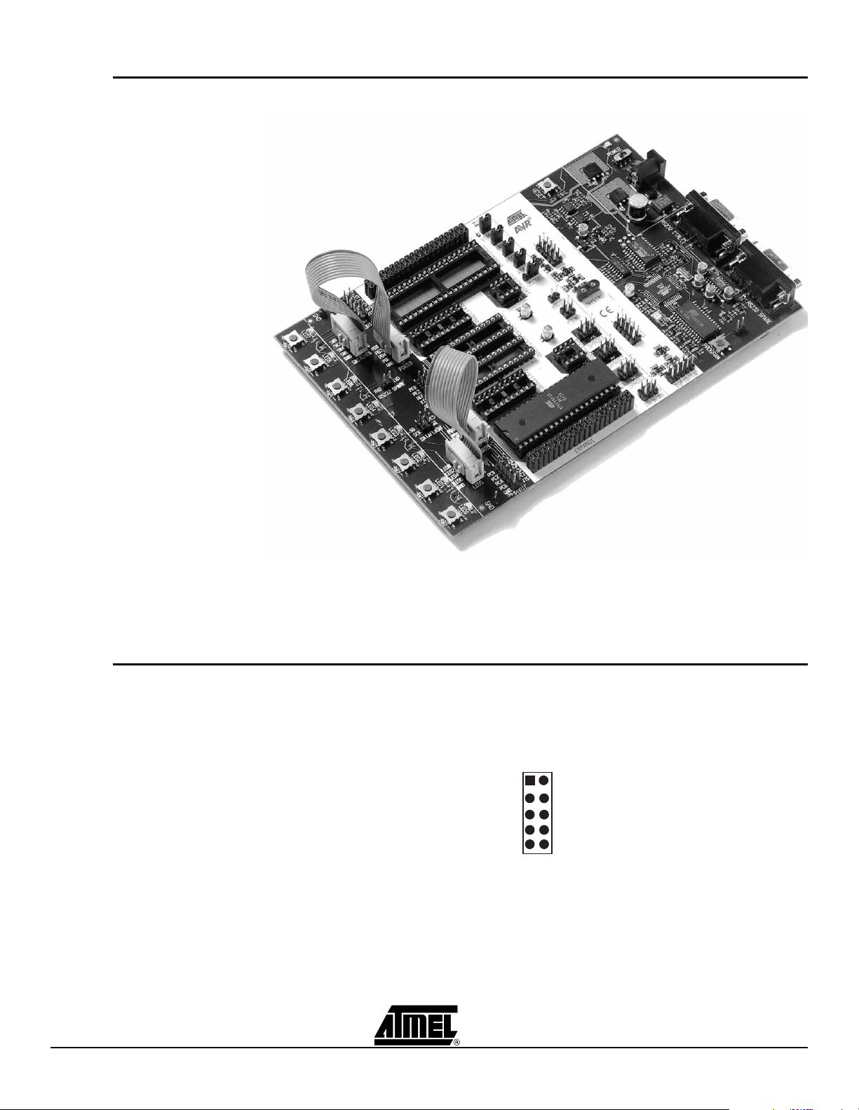
STK500
..............................................................................................
User Guide


Table of Contents
Section 1
Introduction ........................................................................................... 1-1
1.1 Starter Kit Features ...................................................................................1-1
1.2 Device Support .........................................................................................1-2
Section 2
Getting Started......................................................................................2-1
2.1 Unpacking the System ..............................................................................2-1
2.2 System Requirements...............................................................................2-1
2.3 Quick Start ................................................................................................2-2
2.3.1 Connecting the Hardware ...................................................................2-3
2.3.2 Programming the Target AVR Device ................................................2-3
Section 3
Hardware Description ...........................................................................3-1
3.1 Description of User LEDs ..........................................................................3-1
3.2 Description of User Switches ....................................................................3-2
3.3 Connection of LEDs and Switches............................................................3-3
3.4 Port Connectors ........................................................................................3-3
3.5 Description of User RS-232 Interface .......................................................3-5
3.6 Description of DataFlash Pins...................................................................3-6
3.7 Target Socket Section...............................................................................3-8
3.7.1 ISP Programming ...............................................................................3-9
3.7.2 High-voltage Programming...............................................................3-11
3.8 Jumper Settings ......................................................................................3-15
3.8.1 Target V
3.8.2 Analog Reference Voltage, AREF ....................................................3-17
3.8.3 Reset Settings, RESET ....................................................................3-18
3.8.4 Clock Settings, XTAL1 and OSCSEL ...............................................3-20
3.8.5 BSEL2 Jumper .................................................................................3-22
3.8.6 PJUMP Jumpers...............................................................................3-22
3.9 Expansion Connectors ............................................................................3-23
3.9.1 Signal Descriptions ...........................................................................3-25
3.10 Prog Ctrl and Prog Data Headers ...........................................................3-25
3.11 Miscellaneous .........................................................................................3-26
3.11.1 RESET Push Button .........................................................................3-26
3.11.2 PROGRAM Push Button ..................................................................3-27
AVR STK500 User Guide i
Settings, VTARGET .......................................................3-16
CC
1925C–AVR–3/03

Table of Contents
3.11.3 Main Power LED...............................................................................3-27
3.11.4 Target Power LED ............................................................................3-27
3.11.5 Status LED .......................................................................................3-27
Section 4
Installing AVR Studio............................................................................4-1
Section 5
Using AVR Studio................................................................................. 5-1
5.1 Windows Software ....................................................................................5-1
5.2 Starting the Windows Software.................................................................5-1
5.2.1 Starting STK500 .................................................................................5-1
5.3 STK500 User Interface .............................................................................5-2
5.3.1 “Program” Settings .............................................................................5-2
5.3.2 “Fuses” Settings .................................................................................5-3
5.3.3 “LockBits” Settings..............................................................................5-4
5.3.4 “Advanced” Settings ...........................................................................5-4
5.3.5 “Board” Settings..................................................................................5-5
5.3.6 “Auto” Settings ....................................................................................5-7
5.3.7 History Window...................................................................................5-8
5.4 Command Line Software ..........................................................................5-9
5.5 Parameters ...............................................................................................5-9
Section 6
In-System Programming of an External Target System ....................... 6-1
Section 7
Troubleshooting Guide ......................................................................... 7-1
Section 8
Technical Support.................................................................................8-1
Section 9
Example Applications ........................................................................... 9-1
9.1 Using LEDs and Switches.........................................................................9-1
Section 10
Appendix A .........................................................................................10-1
ii AVR STK500 User Guide
1925C–AVR–3/03

Section 1
Introduction
Congratulations on your purchase of the AVR® STK500 Flash Microcontroller Starter
Kit. The STK500 is a complete starter kit and development system for the AVR Flash
Microcontroller from Atmel Corporation. It is designed to give designers a quick start to
develop code on the AVR and for prototyping and testing of new designs.
1.1 Starter Kit Features
n AVR S tudio
n RS-232 Interface to PC for Programming and Control
n Regulated Power Supply for 10 - 15V DC Power
n Sockets for 8-pin, 20-pin, 28-pin, and 40-pin AVR Devices
n Parallel and Serial High-voltage Programming of AVR Devices
n Serial In-System Programming (ISP) of AVR Devices
n In-System Programmer for Programming AVR Devices in External Target System
n Reprogramming of AVR Devices
n 8 Push Buttons for General Use
n 8 LEDs for General Use
n All AVR I/O Ports Easily Accessible through Pin Header Connectors
n Additional RS-232 Port for General Use
n Expansion Connectors for Plug-in Modules and Prototyping Area
n (NB! No longer valid: "On-board 2-Mbit DataFlash
The STK500 is supported by AVR Studio, version 3.2 or higher. For up-to-date information on this and other AVR tool products, please read the document “avrtools.pdf”. The
newest version of AVR Studio, “avrtools.pdf” and this user guide can be found in the
AVR section of the Atmel web site, www.atmel.com.
®
Compatible
®
for Nonvolatile Data Storage")
AVR STK500 User Guide 1-1
Rev. 1925C–AVR–3/03
Introduction
Figure 1-1. STK500
1.2 Device Support The system software currently supports the following devices in all speed grades:
n AT t in y 11 n AT90S4433
n AT t in y 12 n AT90S4434
n AT t in y 15 n AT90S8515
n AT t in y 22 n AT90S8535
n AT t in y 28 n ATmega8
n AT90S1200 n ATmega16
n AT90S2313 n ATmega161
n AT90S2323 n ATmega163
n AT90S2333 n ATmega323
n AT90S2343 n ATmega103
n AT90S4414 n ATmega128
Note: 1. In external target or in STK501, devices do not fit into the sockets of
STK500.
(1)
(1)
Support for new AVR devices may be added in new versions of AVR Studio. The latest
version of AVR Studio is always available from www.atmel.com.
1-2 AVR STK500 User Guide
1925C–AVR–3/03

Section 2
Getting Started
2.1 Unpacking the System
2.2 System Requirements
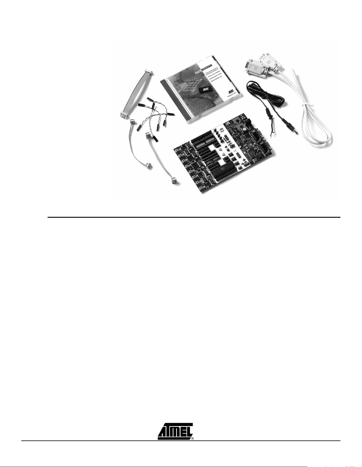
Kit contents:
n STK500 starter kit evaluation board
n Cables for STK500:
– (2 pcs) 10-wire cables for I/O ports and parallel mode programming
– (1 pc) 6-wire cable for In-System Programming
– (4 pcs) 2-wire cable for UART and DataFlash connections
n 9-pin RS-232 cable
n DC power cable
n Atmel CD-ROM with datasheets and software
n AT90S8515-8PC sample microcontroller
The minimum hardware and software requirements are:
n 486 processor (Pentium
n 16 MB RAM
n 12 MB free hard disk space (AVR Studio)
n Windows
®
95/98/2000/ME and Windows NT® 4.0 or higher
®
is recommended)
n 115200 baud RS-232 port (COM port)
n 10 - 15V DC power supply, 500 mA min.
AVR STK500 User Guide 2-1
Rev. 1925C–AVR–3/03
Getting Started
2.3 Quick Start The STK500 starter kit is shipped with an AT90S8515-8PC microcontroller in the socket
marked SCKT3000D3. The default jumper settings will allow the microcontroller to execute from the clock source and voltage regulator on the STK500 board.
The microcontroller is programmed with a test program that toggles the LEDs. The test
program in the AT90S8515 is similar to the example application code described in Section 9. Connect the LEDs and switches and power up the STK500 to run the test
program in the AT90S8515.
Use the supplied 10-pin cables to connect the header marked “PORTB” with the header
marked “LEDS”, and connect the header marked “PORTD” with the header marked
“SWITCHES”. The connections are shown in Figure 2-1.
An external 10 - 15V DC power supply is required. The input circuit is a full bridge rectifier, and the STK500 automatically handles both positive or negative center connectors.
If a positive center connector is used, it can be impossible to turn the STK500 off since
the power switch disconnects the GND terminal. In this case, GND can be supplied
through the RS-232 cable shield if connected or through alternative GND connections.
Connect the power cable between a power supply and the STK500. Apply 10 - 15V DC
to the power connector. The power switch turns the STK500 main power on and off. The
red LED is lit when power is on, and the status LEDs will go from red, via yellow, to
green. The green LED indicates that the target V
ning in the AT90S8515 will respond to pressed switches by toggling the LEDs.
is present. The program now run-
CC
Figure 2-1. Default Setup of STK500
The starter kit can be configured for various clock and power sources. A complete
description of the jumper settings is explained in paragraph 3.8 on page 3-15 and on the
reverse side of the starter kit.
2-2 AVR STK500 User Guide
1925C–AVR–3/03
Getting Started
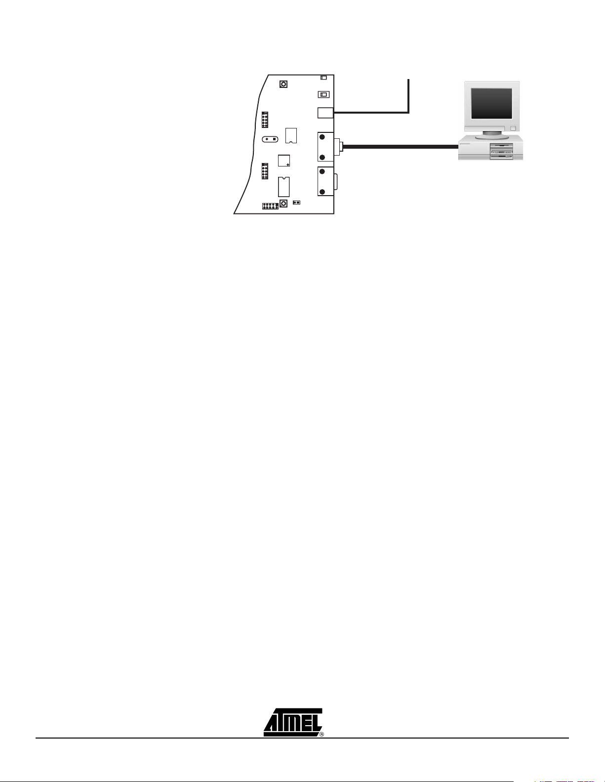
2.3.1 Connecting the Hardware
2.3.2 Programming the Target AVR Device
Figure 2-2. Connection to STK500
10 - 15V DC
To Computer (RS-232)
To program the AT90S8515, connect the supplied 6-wire cable between the ISP6PIN
header and the SPROG3 target ISP header as shown in Figure 2-1. Section 3.7.1 on
page 3-9 describes the programming cable connections.
Connect a serial cable to the connector marked “RS232 CTRL” on the evaluation board
to a COM port on the PC as shown in Figure 2-2. Install AVR Studio software on the PC.
Instructions on how to install and use AVR Studio are given in Section 5 on page 5-1.
When AVR Studio is started, the program will automatically detect to which COM port
the STK500 is connected.
The STK500 is controlled from AVR Studio, version 3.2 and higher. AVR Studio is an
integrated development environment (IDE) for developing and debugging AVR applications. AVR Studio provides a project management tool, source file editor, simulator, incircuit emulator interface and programming interface for STK500.
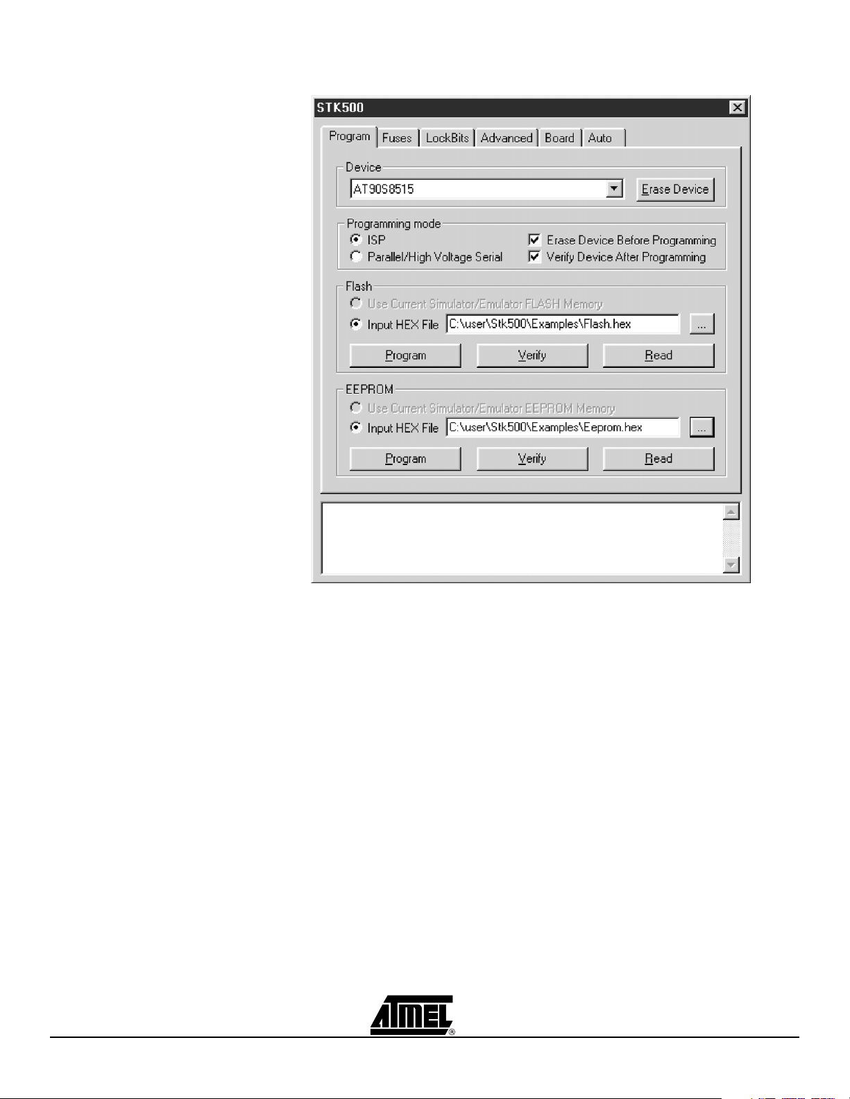
To program a hex file into the target AVR device, select “STK500” from the “Tools”
menu in AVR Studio.
Select the AVR target device from the pull-down menu on the “Program” tab and locate
the intel-hex file to download.
Press the “Erase” button, followed by the “Program” button. The status LED will now
turn yellow while the part is programmed, and when programming succeeds, the LED
will turn green. If programming fails, the LED will turn red after programming. See the
troubleshooting guide in Section 7 on page 7-1.
AVR STK500 User Guide 2-3
1925C–AVR–3/03
Getting Started
Figure 2-3. AVR Studio STK500 Programming Menu
Complete descriptions of using the STK500 interface in AVR Studio are given in Section
5 on page 5-1.
2-4 AVR STK500 User Guide
1925C–AVR–3/03
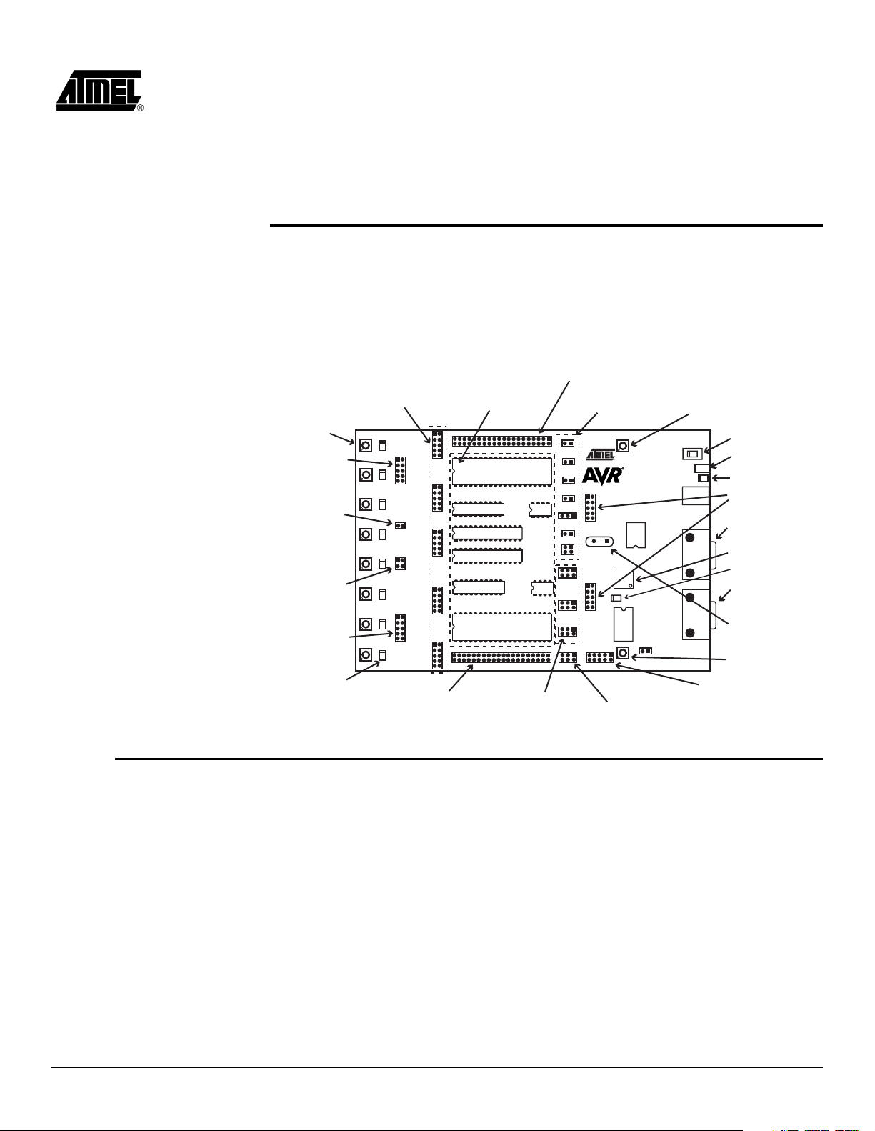
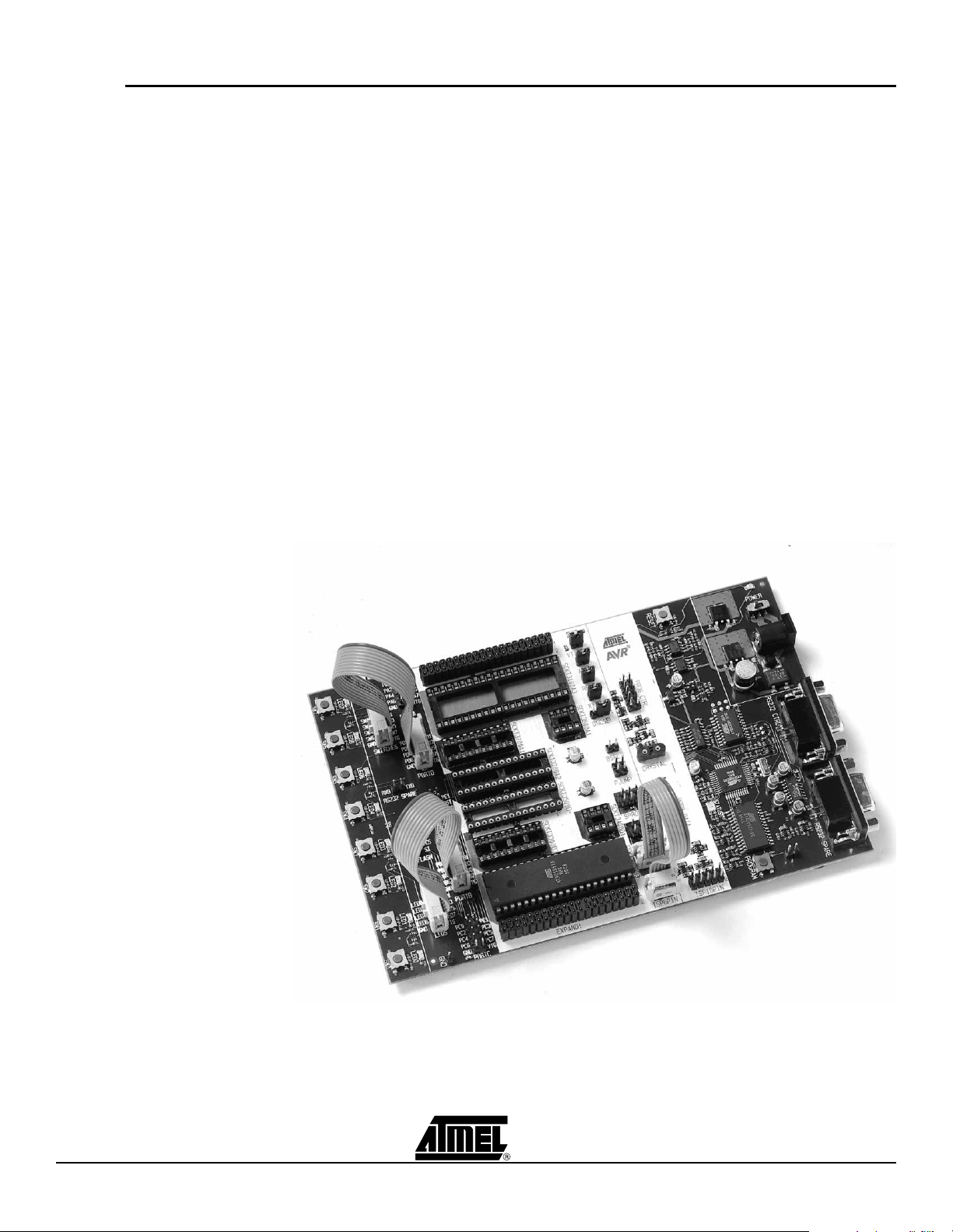
Figure 3-1. STK500 Components
Headers
for I/O Ports
Switches
Header for
Switches
RS-232 Interface
Header
DataFlash Interface
Header
Header for LEDs
Section 3
Hardware Description
Header for
Sockets for
Target AVR
Expansion Boards
Options Setting
Jumpers
Target Reset
Push Button
Power Switch
Power Connector
Parallel Programming
Headers
RS-232 Port
for Programming
Power LED
Master MCU
Status LED
RS-232 Port
for Communication
Socket for
Crystal
Program Button
10-pin ISP Header
(for External Target Only)
3.1 Description of User LEDs
LEDs
Header for
Expansion Boards
Target ISP Headers
6-pin ISP Header
The STK500 starter kit includes 8 yellow LEDs and 8 push-button switches. The LEDs
and switches are connected to debug headers that are separated from the rest of the
board. They can be connected to the AVR devices with the supplied 10-wire cable to the
pin header of the AVR I/O ports. Figure 3-4 shows how the LEDs and switches can be
connected to the I/O port headers. The cables should be connected directly from the
port header to the LED or switch header. The cable should not be twisted. A red wire on
the cable indicates pin 1. Confirm that this is connected to pin 1 on each of the headers.
Figure 3-2 shows how the LED control is implemented. This solution will give the same
amount of light from the LED for all target voltages from 1.8V to 6.0V.
AVR STK500 User Guide 3-1
Rev. 1925C–AVR–3/03
Hardware Description
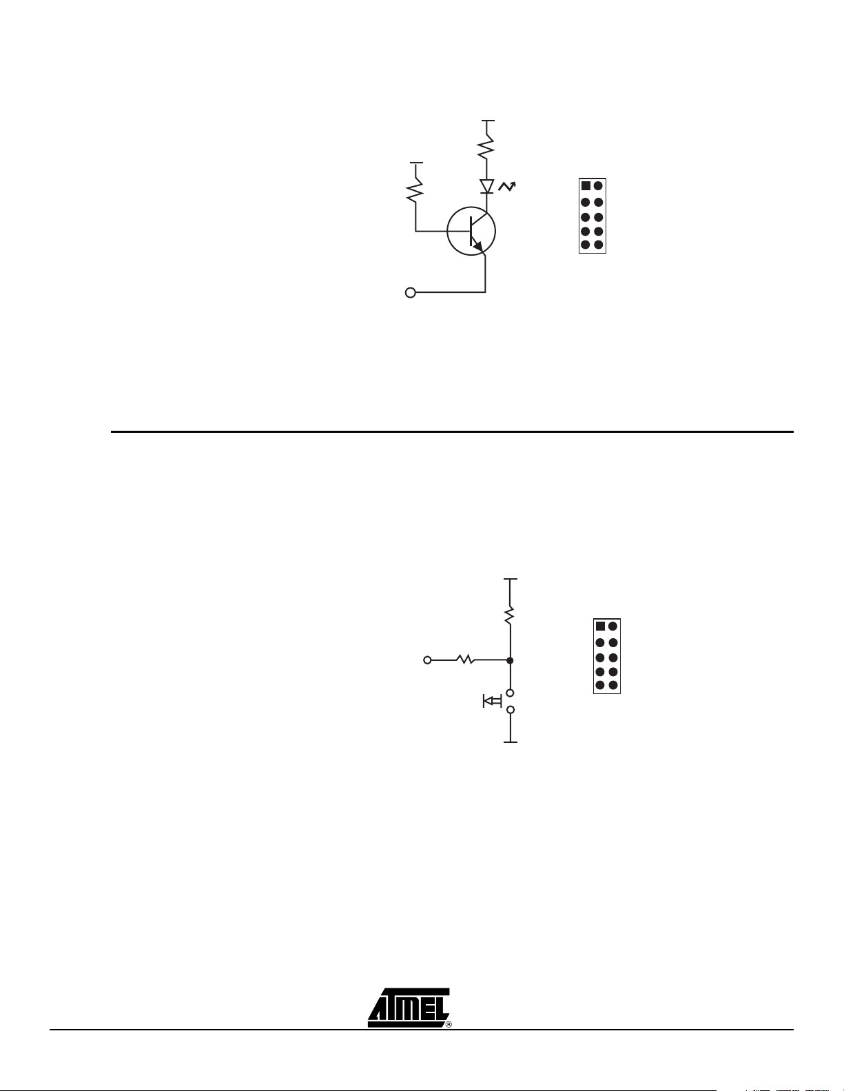
Figure 3-2. Implementation of LEDs and LED Headers
+5V
3.2 Description of User Switches
VTG
10K
LEDn
150R
LED0
LED2
LED4
LED6
GND
1 2
LED1
LED3
LED5
LED7
VTG
Note: The AVR can source or sink enough current to drive a LED directly. In the
STK500 design, a transistor with two resistors is used to give the same amount
of light from the LED, whatever the target voltage (VTG) may be and to turn off
the LEDs when VTG is missing.
The switches connected to the debug headers are implemented as shown in Figure 3-3.
Pushing a switch causes the corresponding SWx to be pulled low, while releasing it will
result in VTG on the appropriate switch header connector. Valid target voltage range is
1.8V < VTG < 6.0V.
Figure 3-3. Implementation of Switches and Switch Headers
VTG
SW0
SW2
SW4
SW6
GND
1 2
SW1
SW3
SW5
SW7
VTG
SW
10K
150R
n
SW
n
Note: In the AVR, the user can enable internal pull-ups on the input pins, removing the
need for an external pull-up on the push-button. In the STK500 design, we have
added an external 10K pull-up to give all users a logical “1” on SWn when the
push-button is not pressed. The 150R resistor limits the current going into the
AVR.
3-2 AVR STK500 User Guide
1925C–AVR–3/03
Hardware Description
3.3 Connection of LEDs and Switches
Figure 3-4. Connection of LEDs and Switches to I/O Port Headers
Any I/O port of the AVR can be connected to the LEDs and switches using the 10-wire
cables. The headers are supplied with VTG (target V
) and GND lines in addition to the
CC
signal lines.
3.4 Port Connectors The pinout for the I/O port headers is explained in Figure 3-5. The square marking indi-
cates pin 1.
Figure 3-5. General Pinout of I/O Port Headers
1 2
Px0
Px2
Px4
Px6
GND
PORTx
The PORTE/AUX header has some special signals and functions in addition to the
PORTE pins. The pinout of this header is shown in Figure 3-6.
Px1
Px3
Px5
Px7
VTG
AVR STK500 User Guide 3-3
1925C–AVR–3/03
Hardware Description
Figure 3-6. Pinout of PORTE Header
1 2
PE0
PE2
REF
XT1
GND
PE1
RST
GND
XT2
VTG
PORTE/AUX
The special functions of this port are:
n PE0 - PE2:
Table 3-1. PORTE Connection
ATmega161 AT90S4414/AT90S8515
PE0 PE0/ICP/INT2 ICP
PE1 PE1/ALE ALE
PE2 PE2/OC1B OC1B
n REF: Analog reference voltage. This pin is connected to the AREF pin on devices
having a separate analog reference pin.
n XT1: XTAL 1 pin. The internal main clock signal to all sockets. If the XTAL1 jumper is
disconnected, this pin can be used as external clock signal.
n XT2: XTAL 2 pin. If the XTAL1 jumper is disconnected, this pin can be used for
external crystal with the XT1 pin.
The headers for the LEDs and switches use the same pinout as the I/O port headers.
The pinout of the switch header is explained in Figure 3-7 and the pinout for the LED
header is explained in Figure 3-8. The square marking indicates pin 1.
Figure 3-7. Pinout of the Switch Header
1 2
SW0
SW2
SW4
SW6
GND
SW1
SW3
SW5
SW7
VTG
SWITCHES
Figure 3-8. Pinout of the LED Header
1 2
LED0
LED2
LED4
LED6
GND
LED1
LED3
LED5
LED7
VTG
LEDS
3-4 AVR STK500 User Guide
1925C–AVR–3/03
Hardware Description
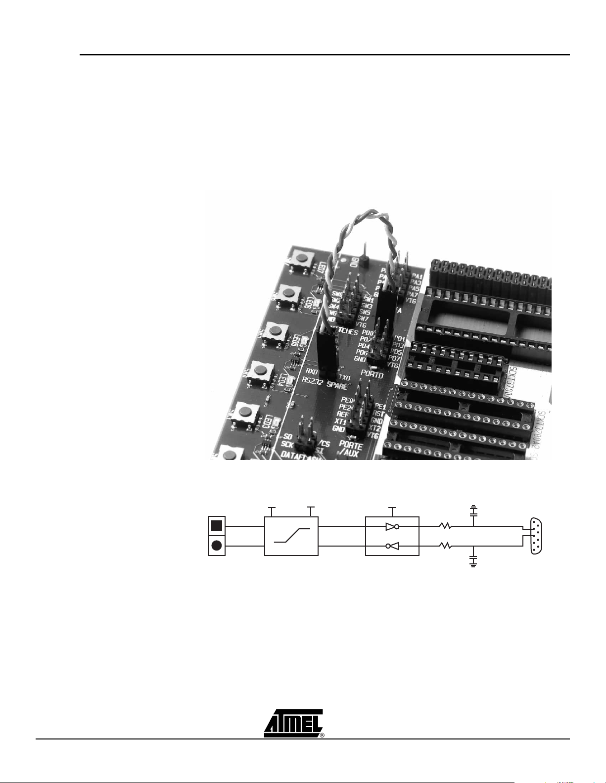
3.5 Description of User RS-232 Interface
The STK500 includes two RS-232 ports. One RS-232 port is used for communicating
with AVR Studio. The other RS-232 can be used for communicating between the target
AVR microcontroller in the socket and a PC serial port connected to the RS-232. To use
the RS-232, the UART pins of the AVR need to be physically connected to the RS-232.
The 2-pin header marked “RS232 SPARE” can be used for connecting the RS-232 converter to the UART pins on the target AVR microcontroller in the socket. Use the 2-wire
cable to connect the UART pins to the RS-232. The connection is shown in Figure 3-9.
The block schematic of the RS-232 connection is shown in Figure 3-10.
Figure 3-9. Connection of I/O Pins to UART
Figure 3-10. Schematic of UART Pin Connections
TXD
RXD
VTG 5V
Voltage
5V
MAX202CSE
470R
470R
1n2
1n2
2
3
RS-232
Converter
AVR STK500 User Guide 3-5
1925C–AVR–3/03
Hardware Description
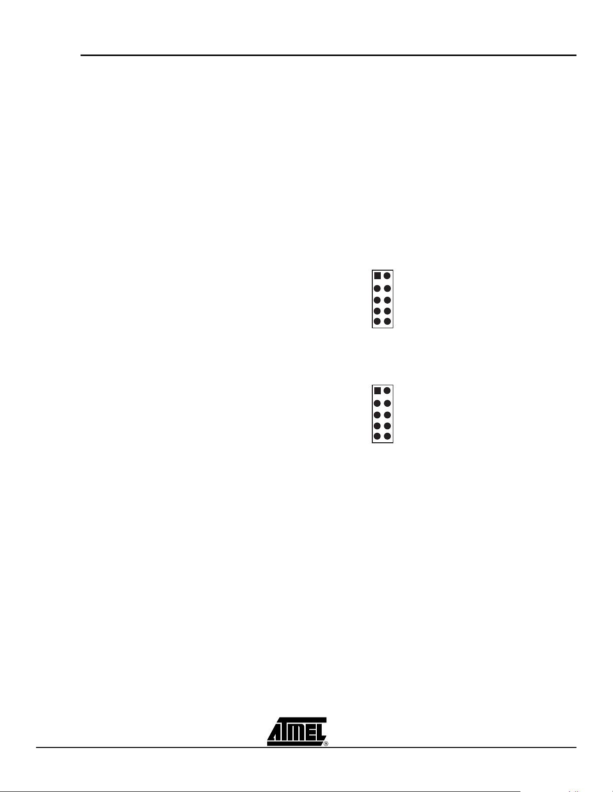
3.6 Description of DataFlash Pins
NB! Not valid: AT45D021 2-Mbit DataFlash is included on the STK500 for data storage.
A DataFlash is a high-density Flash memory with SPI serial interface. A detailed
datasheet of the DataFlash can be obtained from the Flash memory section of the Atmel
CD-ROM or from the Atmel web site.
The DataFlash can be connected to the I/O pins of the microcontroller sockets. The
4-pin header marked “DATAFLASH” can be used for connecting the SPI interface of the
DataFlash to the I/O pins on the target AVR microcontroller in the socket. 2-wire cables
are included with STK500 for connecting the DataFlash to the I/O pins. The supplied
10-wire cables can also be used if the DataFlash is connected to the hardware SPI interface on PORTB of the AVR microcontroller. The connection of the I/O pins is shown in
Figure 3-13. The block schematic of the DataFlash connection is shown in Figure 3-14,
for connection of the DataFlash to the AVR hardware SPI interface. The SPI interface
pinout is shown in Figure 3-11 and Figure 3-12.
Figure 3-11. PORTB SPI Pinout (40-pin Parts)
1 2
PB0
PB2
(SS)PB4
(MISO)PB6
GND
PB1
PB3
PB5(MOSI)
PB7(SCK)
VTG
Figure 3-12. PORTB SPI Pinout (28-pin Analog Parts)
PB0
(SS)PB2
(MISO)PB4
PB6
GND
1 2
PB1
PB3(MOSI)
PB5(SCK)
PB7
VTG
3-6 AVR STK500 User Guide
1925C–AVR–3/03
Figure 3-13. Connection of I/O Pins to DataFlash for AT90S8515
Hardware Description
Figure 3-14. Schematic of DataFlash Connections
VTG 5V
S0
SCK
CS
SI
Voltage
Converter
5V
S0
CS
SI
SCK
AT45D021
DataFlash
AVR STK500 User Guide 3-7
1925C–AVR–3/03
Hardware Description
3.7 Target Socket Section
The programming module consists of the eight sockets in the white area in the middle of
the starter kit. In these sockets, the target AVR devices can be inserted for programming
and are used in the application.
Note: Only one AVR device should be inserted in the sockets at a time.
The AVR Flash memory is guaranteed to be correct after 1,000 programming operations; the typical lifetime of the Flash memory is much longer.
Note: When inserting a device in the socket, notice the orientation of the device.
The notch on the short side of the part must match the notch on the socket. If the device
is inserted the wrong way, it may damage the part and the starter kit.
The socket section is used for both running applications and target device programming.
Figure 3-15. The STK500 Programming Module
The part inserted in the socket can be programmed in the system from AVR Studio with
two different methods:
1. AVR In-System Programming (ISP) running at the parts normal supply voltage.
2. High-voltage Programming, where the supply voltage is always 5 volts.
Four general nets (VTARGET, RESET, XTAL1 and AREF) can be connected to the
socket section.
The following sections describe how to use both programming methods. For instructions
on using the AVR Studio programming software, see Section 5, “Using AVR Studio” on
page 5-1.
3-8 AVR STK500 User Guide
1925C–AVR–3/03

Hardware Description
3.7.1 ISP Programming In-System Programming uses the AVR internal SPI (Serial Peripheral Interface) to
download code into the Flash and EEPROM memory of the AVR. ISP programming
requires only V
, GND, RESET and three signal lines for programming. All AVR
CC
devices except AT90C8534, ATtiny11 and ATtiny28 can be ISP programmed. The AVR
can be programmed at the normal operating voltage, normally 2.7 - 6.0V. No high-voltage signals are required. The ISP programmer can program both the internal Flash and
EEPROM. It also programs fuse bits for selecting clock options, start-up time and internal Brown-out Detector (BOD) for most devices.
High-voltage programming can also program devices that are not supported by ISP programming. Some devices require High-voltage Programming for programming certain
fuse bits. See the High-voltage Programming section on page 3-11 for instructions on
how to use High-voltage Programming.
Because the programming interface is placed on different pins from part to part, three
programming headers are used to route the programming signals to the correct pins. A
6-wire cable is supplied for connecting the ISP signals to the target ISP header. A color
coding system and a number system are used to explain which target ISP header is
used for each socket.
During ISP programming, the 6-wire cable must always be connected to the header
marked “ISP6PIN”. When programming parts in the blue sockets, connect the other end
of the cable to the blue SPROG1 target ISP header. When programming parts in the
green socket, use the green SPROG2 target ISP header. And when programming parts
in the red sockets, use the red SPROG3 target ISP header.Table 3-2 shows which
socket suits which AVR device, and which SPROG target ISP header to use for ISP
programming.
The 6-wire cables should be connected directly from the ISP6PIN header to the correct
SPROG target ISP header. The cable should not be twisted. A colored wire on the cable
indicates pin 1. Confirm that this is connected to pin 1 on each of the headers.
When programming 8-pin devices, note the following: Pin 1 is used both as RESET and
as PB5 on some devices (ATtiny11, ATtiny12 and ATtiny15). Pin 1 on the 8-pin sockets
SCKT3400D1 and SCKT3400D1 are connected to PB5. The RESET signal used during
ISP programming is therefore not connected to pin 1 on these sockets. This signal must
be connected by placing a wire between RST and the PORTE header and PB5 on the
PORTB header.
AVR STK500 User Guide 3-9
1925C–AVR–3/03

Hardware Description
Table 3-2. AVR Sockets
AVR Devices STK500 Socket Color Number Target ISP Header
AT90S1200
AT90S2313
SCKT3300D3 Red 3 SPROG3
AT90S2323
AT90S2343
AT ti ny 1 2
AT ti ny 2 2
SCKT3400D1 Blue 1 SPROG1. Connect RST on
PORTE to PB5 on PORTB.
Connect XTI on PORTE to PB3
(XTAL1 on 2323) on PORTB.
ATtiny11 SCKT3400D1 Blue 1 High-voltage Programming only
ATtiny28 SCKT3500D- None – High-voltage Programming only
AT90S4414
SCKT3000D3 Red 3 SPROG3
AT90S8515
ATmega161
AT90S4434
SCKT3100A3 Red 3 SPROG3
AT90S8535
ATmega16
ATmega163
ATmega323
AT90S2333
SCKT3200A2 Green 2 SPROG2
AT90S4433
AT me ga 8
ATtiny15 SCKT3600A1 Blue 1 SPROG1. Connect RST on
PORTE to PB5 on PORTB.
N/A SCKT3700A1 Blue 1 Socket is not in use in this version
of STK500
ATmega103
Use the STK501 Top Module
ATmega128
Figure 3-16 shows an example of how AT90S2313 can be In-System Programmed. The
6-wire cable is connected from the ISP6PIN header to the red SPROG3 target ISP
header, and the AT90S2313 part is inserted in the red socket marked “SCKT3100D3”.
Figure 3-16. Example Connection for Programming AT90S2313
SPROG1
AVR
SCKT3300D3
SPROG2
SPROG3
ISP6PIN
3-10 AVR STK500 User Guide
1925C–AVR–3/03

Hardware Description
It is not necessary to remove the 6-wire cable from its ISP position while running a program in the AVR. The port pins used for ISP programming can be used for other
purposes in your program.
3.7.2 High-voltage Programming
For High-voltage Programming, a 12V programming voltage is applied to the RESET pin
of the AVR device. All AVR devices can be programmed with High-voltage Programming, and the target device can be programmed while it is mounted in its socket.
Two different methods are used for High-voltage Programming: 8-pin parts use a serial
programming interface, while other parts use a parallel programming interface. The programming signals are routed to the correct pins of the target device using the cables
supplied with STK500.
Table 3-3 summarizes the programming method and special considerations when using
High-voltage Programming.
Table 3-3. High-voltage Programming Settings
AVR
Devices
AT90S1200
AT90S2313
AT90S4414
AT90S8515
AT90S4434
AT90S8535
ATtiny28 SCKT3500D- None –
ATmega161 SCKT3000D3 Red 3 Parallel programming as above; mount
ATmega16
ATmega163
ATmega323
AT90S2333
AT90S4433
STK500
Socket Color Number High-voltage Programming Method
SCKT3300D3 Red 3 Parallel High-voltage Programming.
Connect PROG CTRL header to
SCKT3000D3 Red 3
SCKT3100A3 Red 3
SCKT3100A3 Red 3
SCKT3200A2 Green 2 Parallel programming as above; mount
PORTD and PROG DATA to PORTB,
as shown in Figure 3-17 on page 3-12.
BSEL2 jumper. See Section 3.8.
PJUMP jumpers. See Section 3.8.
ATmega103
ATmega128
ATmega8 SCKT3200A2 Green 2 Parallel programming as above; Mount
AT90S2323
AT90S2343
AT ti ny 1 1
AT ti ny 1 2
AT ti ny 2 2
ATtiny15 SCKT3600A1 Blue 1
N/A SCKT3700A1 Blue 1 Socket not in use in this version of
AVR STK500 User Guide 3-11
Use the
STK501 Top
Module
SCKT3400D1 Blue 1 Serial High-voltage Programming
– – Parallel programming as above; mount
BSEL2 jumper. See Section 3.8.
PJUMP jumpers and mount BSEL2
terminal to PC2. See Section 3.8.5 and
Section 3.8.6.
STK500
1925C–AVR–3/03

Hardware Description
3.7.2.1 Parallel High-voltage Programming
To use High-voltage Programming, the programming signal must be routed to the AVR
I/O pins. The two 10-wire cables supplied with the STK500 can be used to connect the
PROG DATA header to the PORTB header and the PROG CTRL header to the PORTD
header, as shown in Figure 3-17.
Figure 3-17. Connection for Parallel High-voltage Programming
Some of the jumper settings on STK500 must be changed when using High-voltage Programming. Figure 3-18 explains these jumper settings.
3-12 AVR STK500 User Guide
1925C–AVR–3/03

Figure 3-18. Jumper Settings for High-voltage Programming
J
VTARGET
AREF
Hardware Description
umpers
must be
Mounted
Devicedependent
Jumpers
(See Below)
RESET
XTAL1
OSCSEL
BSEL2
PJUMP
Hardware setup for parallel High-voltage Programming:
1. Switch power off.
2. Place the device to program in its socket according to Table 3-3 on page 3-11.
3. Connect the headers PROGDATA and PORTB with the 10-wire cable.
4. Connect the headers PROGCTRL and PORTD with the 10-wire cable.
5. Mount jumper OSCSEL on pins 1 and 2 to select software-controlled clock.
6. Mount jumper XTAL1 to route the oscillator signal to the device.
7. Mount jumpers VTARGET and RESET.
8. When programming AT90S2333, AT90S4433, or ATmega8, mount both PJUMP
jumpers. The 2-wire cables can be used instead of jumpers.
9. When programming ATmega16, ATmega163, ATmega161, ATmega128, or
ATmega323, mount the BSEL2 jumper. When programming ATmega8, connect
BSEL2 terminal to PC2. A 2-wire cable can be used instead of jumpers.
10. Disconnect target system.
11. Switch power on.
12. Ensure that VTARGET is between 4.5V and 5.5V before programming. See Sec-
tion 5.3.5.1.
For a complete description of jumper settings, see Section 3.8, “Jumper Settings”.
Note: Remove the hardware setup for High-voltage Programming before starting a
debug session.
AVR STK500 User Guide 3-13
1925C–AVR–3/03

Hardware Description
3.7.2.2 Serial High-voltage Programming
The 8-pin AVRs have too few pins to use parallel communication during High-voltage
Programming. They use serial communication instead.
This means that fewer signals have to be routed. Hardware setup for serial High-voltage
Programming is as follows:
1. Switch power off.
2. Place the device to program in its socket according to Table 3-3 on page 3-11.
3. Mount jumper OSCSEL on pins 1 and 2 to select software-controlled clock.
4. Mount jumper XTAL1 to route the oscillator signal to the device.
5. Mount jumpers VTARGET and RESET.
6. Use one 2-wire cable to connect the PB3 pin (pin 4) on the PORTB header to the
XT1 pin (pin 7) on the PORTE/AUX header. This will connect the clock system to
the AVR device.
7. Use another 2-wire cable to connect the PB5 pin (pin 6) on the PORTB header to
the RST pin (pin 4) on the PORTE/AUX header. This will connect the reset system to the AVR device.
8. Use a third 2-wire cable to connect the PB0 and PB2 pins (pins 4 and 3) on the
SPROG1 header to the DATA0 and DATA2 pins (pins 1 and 3) on the PROG
DATA header.
9. Use the last 2-wire cable to connect the PB1 pin (pin 1) on the SPROG1 header
to the DATA1 pin (pin 2) on the PROG DATA header.
10. Switch power on and you are ready to program.
All connections are shown in Figure 3-19.
Figure 3-19. Connection for Serial High-voltage Programming
3-14 AVR STK500 User Guide
1925C–AVR–3/03

Hardware Description
3.8 Jumper Settings A master microcontroller and the eight jumpers control the hardware settings of the
starter kit. During normal operation these jumpers should be mounted in the default
position. To configure the starter kit for advanced use, the jumpers can be removed or
set to new positions. The jumper settings and usage are explained in the following section. The default setting of the jumpers are shown in Figure 3-20.
Figure 3-20. Default Jumper Setting
VTARGET
AREF
RESET
XTAL1
OSCSEL
BSEL2
PJUMP
Table 3-4. Description of Jumpers
Jumper Description of Default Setting
VTARGET On-board VTARGET supply connected
AREF On-board Analog Voltage Reference connected
RESET On-board Reset System connected
XTAL1 On-board Clock System connected
OSCSEL On-board Oscillator selected
BSEL2 Unmounted. Used for High-voltage Programming of ATmega8,
ATmega16, ATmega161, ATmega163, ATmega128, and ATmega323
PJUMP Unmounted. Used for High-voltage Programming of AT90S2333,
AT90S4433, and ATmega8
AVR STK500 User Guide 3-15
1925C–AVR–3/03

Hardware Description
3.8.1 Target VCC Settings, VTARGET
VTARGET controls the supply voltage to the target AVR microcontroller sockets. It can
either be controlled from AVR Studio or supplied from an external source. If the VTARGET jumper is mounted, the on-board supply voltage is connected. The on-board
supply voltage can be adjusted to 0 - 6V from AVR Studio. Always verify the respective
datasheet for the AVR device operating voltage before adjusting VTARGET voltage.
Using the on-board supply voltage, approximately 0.5A can be delivered to the target
section. See “Appendix A” in Section 10.
If the VTARGET jumper is disconnected, target V
must be supplied from an external
CC
source at one of the VTG pins on the PORT headers. Figure 3-21 explains VTARGET
jumper options.
When using an external source for VTARGET, the user must control that VTARGET is
at a higher voltage level than AREF (analog reference voltage). Always connect common ground (GND) when using an external VTARGET voltage.
Figure 3-21. VTARGET Jumper Options
Jumper Mounted
VTARGET
AREF
On-board VTARGET supply connected (default)
Jumper not Mounted
VTARGET
AREF
On-board VTARGET supply disconnected
The STK500 master microcontroller controls the target voltage using the internal PWM.
Figure 3-22 shows the internal connection of the VTARGET signal.
Figure 3-22. VTARGET Connection
VTARGET
0 - 6V
Jumper
VTG NET
Green LED
Master
MCU
Rd
Wr
ADC
PWM
10 - 15V
VIN
Voltage
Regulator
Note: The green LED will light when there is a voltage available on the VTG NET. It’s
impossible to use the debug or programming area of STK500 without VTG.
3-16 AVR STK500 User Guide
1925C–AVR–3/03

Hardware Description
The internal VTARGET has a short circuit protection. If VTARGET is set to be higher
than 0.3V and the master microcontroller measures it to be below 0.3V for a duration of
80 ms, the master microcontroller will shut off the VTARGET and the Internal AREF.
When this happens, the status LED will blink quickly.
If an external VTARGET is used and the external VTARGET is turned off, this will also
be detected by the STK500 as a (false) short circuit. The latter case can be avoided by
lowering the internal VTARGET below 0.3V.
3.8.2 Analog Reference Voltage, AREF
The analog reference voltage (AREF) can supply the reference voltage to the on-chip
A/D Converter on the AVR. If the AREF jumper is mounted, the on-board analog reference voltage is connected to the AVR’s AREF. The on-board analog reference voltage
can be adjusted from AVR Studio to 0 - 6.0V, but not above VTARGET.
When the AREF jumper is disconnected, AREF voltage must be supplied from an external source at the AREF pin on the PORTE/AUX header (Figure 3-6). Figure 3-23
explains AREF jumper options.
When using an external source for AREF, the user must control VTARGET at a higher
voltage level than AREF. This can be controlled easily by reading the VTG value from
AVR Studio before setting AREF.
Figure 3-23. AREF Jumper Options
Jumper Mounted
VTARGET
AREF
RESET
On-board AREF voltage connected (default)
Jumper not Mounted
VTARGET
AREF
RESET
On-board AREF voltage disconnected
The STK500 master microcontroller controls the analog reference voltage using the
internal PWM. The AVR’s AREF signal is also accessible on the PORTE header; this
pin can also be used for external AREF signal. Figure 3-24 shows the internal connection of the AREF signal.
AVR STK500 User Guide 3-17
1925C–AVR–3/03

Hardware Description
Figure 3-24. Internal AREF Connection
3.8.3 Reset Settings, RESET
AREF
Jumper
AREF
1 2
PE0
PE2
REF
XT1
GND
PORTE/AUX
PE1
RST
GND
XT2
VTG
Master
MCU
Rd
Wr
ADC
PWM
10 - 15V
VIN
Voltage
regulator
0 - 6V
The AVR Studio-controlled analog reference voltage can also be used as an input to the
analog comparator or for ADC measurements on the AVR. AVR’s AREF signal can then
be connected to VTG.
The internal AREF has a short circuit protection. If an AREF value is set up to be higher
than 0.3V and the master microcontroller measures it to be below 0.3V for a duration of
80 ms, the master microcontroller will shut off the AREF. When this happens, the status
LED will blink slowly.
The AREF will also be shut down by the master microcontroller if a short circuit is
detected on VTARGET (in addition to shutting down VTARGET). In this case, the status
LED will blink quickly.
The RESET jumper controls the RESET signal to the STK500. When ISP programming
the target device in the socket, the master microcontroller programs the AVR device
without interfering with the application. When the RESET jumper is mounted, the master
microcontroller controls the RESET signal of the AVR. When the RESET jumper is not
mounted, the RESET signal is disconnected. This is useful for prototype applications
with an external reset system.
The RESET jumper must always be mounted when High-voltage Programming an AVR
device. When using an external reset system, it must allow the reset line to be controlled
by the master microcontroller reset system during programming. The RESET button is
disconnected if the RESET jumper is not mounted. Figure 3-25 explains the RESET
jumper options.
3-18 AVR STK500 User Guide
1925C–AVR–3/03

Figure 3-25. RESET Jumper Options
Jumper Mounted
AREF
RESET
XTAL1
On-board RESET Signal Connected (default)
Jumper not Mounted
AREF
RESET
XTAL1
Hardware Description
On-board RESET Signal Disconnected
The STK500 master microcontroller controls the RESET signal to the target AVR. The
RESET signal is accessible on the PORTE/AUX header; this pin can also be used for
external RESET signal. Figure 3-26 shows the internal connection of the RESET signal.
Figure 3-26. Internal RESET Connection
Master
MCU
RESET
RESET
CIRCUIT
0V - VTG - 12V
1 2
PE0
PE2
REF
XT1
GND
RESET
RESET NET
Jumper
PE1
RST
GND
XT2
VTG
PORTE/AUX
Note: During High-voltage Programming, STK500 applies 12V to the AVR’s RESET
line. Thus, an external reset circuit not capable of handling this must be disconnected before High-voltage Programming the AVR.
AVR STK500 User Guide 3-19
1925C–AVR–3/03

Hardware Description
When connected to an external system, there is often an external pull-up resistor connected to the reset line. A typical reset connection is shown in Figure 3-27.
Figure 3-27. External Reset Connection
R (4.7 kohm)
RESET
C (10 nF)
If the external pull-up resistor is too low (<4.7 kΩ), STK500 will not be able to pull the
RESET line low.
3.8.4 Clock Settings, XTAL1 and OSCSEL
STK500 includes several clock options for the target AVR. Setting the jumpers XTAL1
and OSCSEL controls the clock selections. OSCSEL determines what signal to route to
the XTAL1 pin of the AVR.
When the XTAL1 jumper is connected, the STK500 internal clock system is used as
main clock to the target AVR. When XTAL1 jumper is not mounted, the internal clock
system is disconnected. This allows external clock signals or crystals to be used as target clock source for the AVR. Figure 3-28 illustrates the XTAL1 jumper option.
Figure 3-28. XTAL1 Jumper Options
Jumper Mounted
AREF
RESET
XTAL1
OSCSEL
On-board XTAL1 Signal Connected (Default)
Jumper not Mounted
AREF
RESET
XTAL1
OSCSEL
On-board XTAL1 Signal Disconnected
When the XTAL1 jumper is not mounted, an external clock source or crystal can be connected to the PORTE header. This is shown in Figure 3-30.
3-20 AVR STK500 User Guide
1925C–AVR–3/03

Hardware Description
When the XTAL1 jumper is mounted, the STK500 internal clock system is used as main
clock to the target AVR. The internal clock system can either use a crystal in the
on-board crystal socket or a software-generated clock from the master microcontroller.
The frequency of the software-generated clock can be set from 0 to 3.68 MHz. The
default value is 3.68 MHz. Section 5.3.5.3 on page 5-7 explains how to set the clock frequency from AVR Studio.
When using the STK500 software-generated clock system as main clock, the target
AVR microcontroller fuses should be configured for “external clock” as clock source.
This gives shortest start-up time for the microcontroller. For details of start-up time, see
the datasheet for the AVR microcontroller. For an explanation of clock source fuses configuration, see Section 5.3.2 on page 5-3. Not all AVR devices have fuses for selection
between using a crystal or oscillator as clock source.
The internal clock system is selected with the OSCSEL jumper. Figure 3-29 shows the
jumper options for OSCSEL.
The on-board oscillator will work with ceramic resonators or crystals between
2 - 20 MHz (AT-cut, fundamental and parallel resonant crystals).
Figure 3-29. OSCSEL Jumper Options
Jumper mounted on pins 1 and 2
XTAL1
OSCSEL
On-board software clock signal connected (default)
Jumper mounted on pins 2 and 3
XTAL1
OSCSEL
On-board crystal signal connected
Jumper not mounted
XTAL1
OSCSEL
On-board XTAL1 signal disconnected
When programming AVR in High-voltage Programming mode, OSCSEL should be
mounted on pins 1 and 2 to give the master microcontroller control of the target clock.
This is explained in detail in Section 3.7.2 on page 3-11.
Note: In a real application with only one AVR connected to the crystal, there is no
need for an external oscillator circuit. The STK500 has eight different AVR
sockets connected to the same clock system. The long signal lines in this
system makes it difficult to drive a crystal with the On-chip Oscillators on the
AVR. The oscillator on STK500 is designed to operate on all target voltages
from 1.8 to 6.0V.
AVR STK500 User Guide 3-21
1925C–AVR–3/03

Hardware Description
Figure 3-30. XTAL1 and OSCSEL Connections
CRYSTAL
AVR
Studio
Oscillator
OSCSEL
3
2
1
Jumper
MASTER
MCU
VTG5V
Voltage
converter
XTAL1
Jumper
XTAL1 NET
PE0
PE2
REF
XT1
GND
1 2
PE1
RST
GND
XT2
VTG
PORTE
3.8.5 BSEL2 Jumper The BSEL2 jumper connects the Byte Select 2 signal for High-voltage Programming of
ATmega8, ATmega16, ATmega161, ATmega163, ATmega128, and ATmega323. The
BSEL2 jumper should only be mounted when High-voltage Programming ATmega16,
ATmega161, ATmega163, ATmega128, or ATmega323. When using ATmega8, connect the right BSEL2 pin to PC2 in the target area. See Figure 3-31. For descriptions of
the Byte Select 2 signal, see the programming section of the corresponding parts
datasheet.
Figure 3-31. BSEL2 Connection for ATmega8
Cable to PC2
BSEL2
PJUMP
3.8.6 PJUMP Jumpers The PJUMP jumpers route the programming pin of AT90S2333, AT90S4433, and
ATmega8 to the programming lines when using High-voltage Programming. The
PJUMP jumpers should only be mounted when using High-voltage Programming on
AT90S2333, AT90S4433, or ATmega8. During debugging, High-voltage Programming
of other parts and ISP programming, these jumpers should not be mounted.
Figure 3-32. PJUMP Jumpers Placement
Correct
Jumper
Placement
Not
Correct
3-22 AVR STK500 User Guide
1925C–AVR–3/03

Hardware Description
3.9 Expansion Connectors
STK500 has two expansion connectors, one on each side of the programming module.
All AVR I/O ports, programming signals and control signals are routed to the expansion
connectors. The expansion connectors allow easy prototyping of applications
with STK500. The pinout of the expansion connectors is shown in Figure 3-34 and Figure 3-35.
Figure 3-33. Expansion Headers
Expansion Header 0
Pin 1
Prog Ctrl
Expansion Header 1
Pin 1
Prog Data
AVR STK500 User Guide 3-23
1925C–AVR–3/03

Hardware Description
Figure 3-34. Expansion Connector 0 Pinout
CT7
CT5
CT3
CT1
NC
RST
PE1
VTG
PC7
PC5
PC3
PC1
PA7
PA5
PA3
PA1
1
3
5
7
9
11
13
15
17
19
21
23
25
27
29
31
33
35
37
39
GND
AUXI0
GND
GND
Figure 3-35. Expansion Connector 1 Pinout
10
12
14
16
18
20
22
24
26
28
30
32
34
36
38
40
2
4
6
8
GND
AUXO0
CT6
CT4
CT2
BSEL2
REF
PE2
PE0
GND
VTG
PC6
PC4
PC2
PC0
PA6
PA4
PA2
PA0
GND
GND
AUXI1
DATA7
DATA5
DATA3
DATA1
SCK
XT1
VTG
GND
PB7
PB5
PB3
PB1
PD7
PD5
PD3
PD1
GND
1
3
5
7
9
11
13
SI
15
17
19
21
23
25
27
29
31
33
35
37
39
10
12
14
16
18
20
22
24
26
28
30
32
34
36
38
40
2
4
6
8
GND
AUXO1
DATA6
DATA4
DATA2
DATA0
SO
CS
XT2
VTG
GND
PB6
PB4
PB2
PB0
PD6
PD4
PD2
PD0
GND
3-24 AVR STK500 User Guide
1925C–AVR–3/03

Hardware Description
3.9.1 Signal Descriptions The signals AUXI1, AUXI0, AUXO1, and AUXO0 are intended for future use. Do not connect these signals to your application.
The DATA[7:0] and CT[7:1] signals are also found on the Prog Data and Prog Ctrl connectors. These signals and connectors are explained in Section 3.10 on page 3-25.
The BSEL2 signal is the same as that found on the BSEL2 jumper. This jumper is
explained in Section 3.8.5 on page 3-22.
3.10 Prog Ctrl and
Prog Data
Headers
The SI, SO, SCK, and CS
signals are connected to the DataFlash. Use of the DataFlash
is described in Section 3.6 on page 3-6.
NC means that this pin is not connected.
The remaining signals are equal to those found on the PORT connectors, explained in
Section 3.4 on page 3-3.
Note: DATA, CT, and AUX signals are based on 5V CMOS logic. No voltage conver-
sion to adapt to VTG is done on these signals.
The Prog Ctrl and Prog Data headers are used for High-voltage Programming of the target AVR device. The placement of the headers is shown in Figure 3-33. During parallel
High-voltage Programming, the Prog Ctrl signals are routed to PORTD of the target
device. The Prog Data signals are routed to PORTB. See Section 3.7.2 on page 3-11 for
a complete description of High-voltage Programming. The pinouts of the Prog Ctrl and
Prog Data headers are shown in Figure 3-36 and Figure 3-37. For more information
about High-voltage Programming of AVR devices, see the programming section of each
AVR datasheet.
Note: Prog Ctrl and Data connectors are connected directly to the master microcon-
troller without level converters. This means that these signals are always 5V
logic.
Figure 3-36. Prog Ctrl Header Pinout
1 2
NC
(OE)CT2
(BS1)CT4
(XA1)CT6
GND
CT1(RDY/BSY)
CT3(/WR)
CT5(XA0)
CT7(PAGEL)
NC
The Prog Ctrl signals are normally used for the control signals when parallel Highvoltage Programming an AVR device.
Note: All Prog Ctrl signals are based on 5V CMOS logic. No voltage conversion to
adapt to VTG is done on these signals.
AVR STK500 User Guide 3-25
1925C–AVR–3/03

Hardware Description
Figure 3-37. Prog Data Header Pinout
1 2
DATA0
DATA2
DATA4
DATA6
GND
DATA1
DATA3
DATA5
DATA7
NC
The Prog Data signals are used for the data bus when parallel High-voltage Programming an AVR device. During ISP programming, DATA5 is used as MOSI, DATA6 is
used as MISO, and DATA7 is used for SCK.
Note: All Prog Data signals are based on 5V CMOS logic. No voltage conversion to
adapt to VTG is done on these signals.
3.11 Miscellaneous STK500 has 2 push buttons and 3 LEDs for special functions and status indication. The
following section explains these features. Figure 3-38 shows the placement of these
functions.
Figure 3-38. Special Functions and Status Indication LEDs
Target Power LED
RESET Push Button
Main Power LED
Status LED
Program Push Button
3.11.1 RESET Push Button The RESET push button resets the target AVR device when pushed. The master microcontroller is not controlled by the RESET push button. When the RESET jumper is not
mounted, the RESET push button is disabled.
3-26 AVR STK500 User Guide
1925C–AVR–3/03

Hardware Description
3.11.2 PROGRAM Push
Button
Future versions of AVR Studio may upgrade the master microcontroller on STK500.
AVR Studio will then detect old software versions of STK500 and update the Flash program memory of the master microcontroller. To do this, the user is required to push the
PROGRAM button when powering on STK500. AVR Studio issues instructions on how
to perform the upgrade during the upgrade process.
3.11.3 Main Power LED The red power LED is directly connected to the STK500 main power supply. The power LED is always lit when power is applied to STK500.
3.11.4 Target Power LED The target power LED is connected to VCC lines (VTG) on the target AVR devices in the sockets. The target power LED is lit when power is applied to the target AVR device.
3.11.5 Status LED The PROGRAM LED is a 3-color LED. During programming, the LED is yellow. When the target AVR device is successfully programmed, the LED will turn green. If programming fails, the LED will turn red to indicate that programming failed. When programming fails, check the troubleshooting guide in Section 7 on page 7-1. During start-up, the status LED will shift from red, through yellow, to green to indicate that the master microcontroller is ready.
AVR STK500 User Guide 3-27
1925C–AVR–3/03

Hardware Description
3-28 AVR STK500 User Guide
1925C–AVR–3/03

Section 4
Installing AVR Studio
AVR Studio, with its Integrated Development Environment (IDE), is the ideal software
for all AVR development. It has an editor, an assembler and a debugger and is front-end
for all AVR emulators and the STK500 starter kit.
To install AVR Studio, insert the supplied Atmel CD-ROM databook in the computer and
navigate to “Products → AVR 8-bit RISC → Software”. Right-click with the mouse on the
“AVRstudio.exe” file and select “save link as”. Select an empty directory and save the
file.
Execute the “AVRstudio.exe” file; this is a self-extracting file that will extract all required
files to the current directory. Execute the “Setup.exe” file; this will guide you through the
setup process.
Note: AVR Studio, version 3.2 or higher, is required for STK500 support.
AVR STK500 User Guide 4-1
Rev. 1925C–AVR–3/03

Installing AVR Studio
4-2 AVR STK500 User Guide
1925C–AVR–3/03

Section 5
Using AVR Studio
5.1 Windows
Software
5.2 Starting the
Windows Software
5.2.1 Starting STK500 Pressing the “AVR” button on the AVR Studio toolbar will start the STK500 user inter-
In this section, the supporting software for STK500 will be presented and an in-depth
description of the available programming options is given.
The software used for communicating with the STK500 development board is included
in AVR Studio, version 3.2 and higher. For information on how to install this software,
please see Section 4 on page 4-1. Once installed, AVR Studio can be started by doubleclicking on the AVR Studio icon. If default install options are used, the program is
located in the Windows “Start menu → Programs → Atmel AVR Tools” folder.
face as shown in Figure 5-1.
Figure 5-1. AVR Studio with STK500 User Interface
AVR STK500 User Guide 5-1
Rev. 1925C–AVR–3/03

Using AVR Studio
5.3 STK500 User
Interface
The STK500 user interface includes powerful features for the STK500 development
board. The available settings are divided into six groups, each selectable by clicking
on the appropriate tab. Since different devices have different features, the available
options and selections will depend on which device is selected. Unavailable features are
grayed out.
5.3.1 “Program” Settings The program settings are divided into four different subgroups.
5.3.1.1 Device A device is selected by selecting the correct device from the pull-down menu. This
group also includes a button that performs a chip erase on the selected device, erasing
both the Flash and EEPROM memories.
5.3.1.2 Programming Mode This group selects programming mode. For devices only supporting High-voltage Programming, the ISP option will be grayed out. If both modes are available, select a mode by clicking on the correct method. Checking “Erase Device Before Programming” will force STK500 to perform a chip erase before programming code to the program memory (Flash). Checking “Verify Device After Programming” will force STK500 to perform a verification of the memory after programming it (both Flash and EEPROM).
5.3.1.3 Flash If the STK500 user interface is opened without a project loaded in AVR Studio, the “Use Current Simulator/Emulator FLASH Memory” option will be grayed out. When a project is open, this option allows programming of the Flash memory content currently present in the Flash Memory view of AVR Studio. For more information about AVR Studio memory views, please take a look in the AVR Studio Help file.
If no project is running, or the source code is stored in a separate hex file, select the
“Input HEX File” option. Browse to the correct file by pressing the button or type the
complete path and filename in the text field. The selected file must be in “Intel-hex” format or “extended Intel-hex” format.
Figure 5-2. Program
5-2 AVR STK500 User Guide
1925C–AVR–3/03

Using AVR Studio
5.3.1.4 EEPROM If the STK500 user interface is opened without a project loaded in AVR Studio, the “Use Current Simulator/Emulator EEPROM Memory” option will be grayed out. When a project is open, this option allows programming of the EEPROM memory content currently present in the EEPROM Memory view. For more information about AVR Studio memory views, please take a look in the AVR Studio Help file.
If no project is running, or the source code is stored in a separate hex file, select the
“Input HEX File” option. Browse to the correct file by pressing the button or type the
complete path and filename in the text field. The selected file must be in “Intel-hex” format or “extended Intel-hex” format.
5.3.2 “Fuses” Settings In the “Fuses” tab an overview of accessible fuses are presented. Some fuses are only available during High-voltage Programming. These will be displayed but not accessible if operating in ISP programming mode. Press the “Read” button to read the current value of the fuses, and the “Write” button to write the current fuse setting to the device. Checking one of these check boxes indicates that this fuse should be enabled/programmed, which means writing a “0” to the fuse location in the actual device. Note that the selected fuse setting is not affected by erasing the device with a chip-erase cycle (i.e., pressing “Chip Erase” button in the “Program” settings).
Detailed information on what fuses are available in the different programming modes
and their functions can be found in the appropriate device datasheet.
Figure 5-3. Fuses
AVR STK500 User Guide 5-3
1925C–AVR–3/03

Using AVR Studio
5.3.3 “LockBits” Settings Similar to the “Fuses” tab, the “LockBits” tab shows which lock modes are applicable to the selected device. All lock bits are accessible in both ISP and High-voltage Programming. A lock mode may consist of a combination of setting multiple Lock bits. This is handled by the STK500 user interface, and the correct lock bits are programmed automatically for the selected lock mode. Once a Lock mode protection level is enabled, it is not possible to lower the protection level by selecting a “lower” degree of protection or by setting a different Lock mode. The only way to remove a programmed Lock bit is to perform a complete chip erase, erasing both program and data memories. One exception exists: If the target device has a programmed “EESAVE” fuse, the contents of the EEPROM will be saved even though a complete chip erase on the device is performed.
Figure 5-4. LockBits
5.3.4 “Advanced”
The “Advanced” tab is currently divided into two subgroups.
Settings
5.3.4.1 Signature Bytes By pressing the “Read Signature” button, the signature bytes are read from the target
device. The signature bytes act like an identifier for the part. After reading the signature,
the software will check if it is the correct signature according to the chosen device.
Please refer to the AVR datasheets to read more about signature bytes.
5-4 AVR STK500 User Guide
1925C–AVR–3/03

Figure 5-5. Advanced
Using AVR Studio
5.3.4.2 Oscillator
Calibration Byte
The oscillator calibration byte is written to the device during manufacturing, and cannot
be erased or altered by the user. The calibration byte is a tuning value that should be
written to the OSCCAL register in order to tune the internal RC oscillator.
5.3.4.3 Reading Oscillator
Calibration Byte
By pressing the “Read Cal. Byte” button, the calibration value is read from the device
and is shown in the “Value” text box. Note that the calibration byte is not directly accessible during program execution and must be written to a memory location during
programming if it shall be used by the program. If this option is grayed out, the selected
device does not have a tunable internal RC oscillator.
5.3.4.4 Writing Oscillator
Calibration Byte
Since the calibration byte is not directly accessible during program execution, the user
should write the calibration byte into a known location in Flash or EEPROM memory. Do
this by writing the desired memory address in the “Write Address” text box and then
press the “Write to Memory” button. The calibration byte is then written to the memory
indicated by the “Flash” and “Eeprom” radio buttons.
5.3.5 “Board” Settings The “Board” tab allows the changing of operating conditions on the STK500 development board. The following properties can be modified: VTARGET, AREF and oscillator frequency.
The interface is very flexible and it is possible to force the operating conditions beyond
the recommended specifications for the device. Doing this is not recommended, and
may damage the target device. The recommended operating conditions for the part are
stated in the device datasheet.
AVR STK500 User Guide 5-5
1925C–AVR–3/03

Using AVR Studio
Figure 5-6. Board
5.3.5.1 VTARGET VTARGET controls the operating voltage for the target board. Through the use of the slide bar or the text box, this voltage can be regulated between 0 and 6.0V in 0.1V increments. Please refer to the device datasheet to find the specified voltage range for the selected device. Both voltages are read by pressing the “Read Voltages” button, and written by pressing the “Write Voltages” button.
The physical connection of the VTARGET voltage is shown in Figure 3-22 on page 3-16.
5.3.5.2 AREF AREF controls the analog reference voltage for the ADC converter. This setting only apply to devices with AD converter. Through the use of the slide bar or the text box, this voltage can be regulated between 0 and 6.0V in 0.1V increments. Please refer to the device datasheet to find the valid voltage range for the selected device. Both VTARGET and AREF are read by pressing the “Read Voltages” button, and written by pressing the “Write Voltages” button.
It is not possible to set AREF to a higher voltage than VTARGET because this will permanently damage the AVR.
The physical connection of the AREF voltage is shown in Figure 3-24 on page 3-18.
5-6 AVR STK500 User Guide
1925C–AVR–3/03

Using AVR Studio
5.3.5.3 Oscillator The STK500 development board uses a programmable oscillator circuit that offers a wide range of frequencies for the target device.
Since it is not possible to generate an unlimited number of frequencies, the STK500
user interface will calculate the value closest to the value written to the oscillator text
box. The calculated value is then presented in the oscillator text box, overwriting the
previously written number.
5.3.6 “Auto” Settings When programming multiple devices with the same code, the “Auto” tab offers a powerful method of automatically going through a user-defined sequence of commands. The commands are listed in the order they are executed (if selected). To enable a command, the appropriate check box should be checked. For example, if only “Program FLASH” is checked when the “Start” button is pressed, the Flash memory will be programmed with the hex file specified in the “Program” settings. All commands depend on and use the settings given in the STK500 user interface.
Figure 5-7. Auto
It is possible to log the command execution to a text file by checking the “Log to file”
check box.
AVR STK500 User Guide 5-7
1925C–AVR–3/03

Using AVR Studio
5.3.6.1 Setting Up the
System for
Auto-programming
Click on the check boxes for the commands that you want the STK500 user interface to
perform. A typical sequence where the device is erased and then programmed is shown
in Figure 5-7. The chip is erased, both memories programmed and verified, and finally,
fuses and lock bits are programmed.
Once configured, the same programming sequence is executed every time the “Start”
button is pressed. This reduces both work and possibilities for errors due to operational
errors.
5.3.6.2 Logging the
Auto-programming
to a File
By clicking on the “Log to file” check box, all output from the commands are written to a
text file. Select or create the file by pressing the “Browse” button and navigate to the
location where the file is placed or should be created. The output is directed to this file,
and can be viewed and edited using a text editor.
5.3.7 History Window The History window is located at the bottom of the STK500 view. In this window the dialog between AVR Studio and STK500 is shown. For every new command performed,
the old dialog is replaced with the new one.
Figure 5-8. History Window
5-8 AVR STK500 User Guide
1925C–AVR–3/03

Using AVR Studio
5.4 Command Line
Software
The DOS command line version of the STK500 software is useful for programming
STK500 from external editors or for use in production programmers. Simple batch files
can be made for automatic programming. Type “STK500 -?” for help.
The program returns ERRORCODE 0 if the operation was successful, and ERRORCODE 1 if the operation failed.
Command Line Switches:
[-d device name] [-m s|p] [-if infile] [-ie infile] [-of outfile]
[-oe outfile] [-s] [-O] [-Sf addr] [-Seaddr] [-e] [-p f|e|b]
[-r f|e|b] [-v f|e|b] [-l value] [-L value] [-y] [-f value] [-E value]
[-F value] [-G value] [-q] [-x value] [-af start,stop] [-ae start,stop]
[-c port] [-ut value] [-ua value] [-wt] [-wa] [-b h|s] [-! freq] [-t]
[-g] [-z] [-h|?]
5.5 Parameters d Device name. Must be applied when programming the device. See list below.
m Select programming mode; serial (s) or parallel/High-voltage (p).
Serial programming mode is the default, and is used if this parameter not
applied.
if Name of FLASH input file. Required for programming or verification of the FLASH
memory. The file format is Intel Extended HEX.
ie Name of EEPROM input file. Required for programming or verification of the
EEPROM memory. The file format is Intel Extended HEX.
of Name of flash output file. Required for readout of the FLASH memory. The file
format is Intel Extended HEX.
oe Name of EEPROM output file. Required for readout of the EEPROM memory. The
file format is Intel Extended HEX.
s Read signature bytes.
O Read oscillator calibration byte.
Sf Write oscillator call. byte to FLASH memory. “addr” is byte address
Se Write oscillator call. byte to EEPROM memory. “addr” is byte address
e Erase device. If applied with another programming parameter, the device will be
erased before any other programming takes place.
p Program device; FLASH (f), EEPROM (e) or both (b). Corresponding input files
are required.
r Read out device; FLASH (f), EEPROM (e) or both (b). Corresponding output files
are required
v Verify device; FLASH (f), EEPROM (e) or both (b). Can be used with -p or stand
alone. Corresponding input files are required.
l Set lock byte. “value' is an 8-bit hex. value.
L Verify lock byte. “value” is an 8-bit hex. value to verify against.
y Read back lock byte.
AVR STK500 User Guide 5-9
1925C–AVR–3/03

Using AVR Studio
f Set fuse bytes. “value” is a 16-bit hex. value describing the settings for the upper
and lower fuse.
E Set extended fuse byte. “value” is an 8-bit hex. value describing the extend fuse
settings.
F Verify fuse bytes. “value” is a 16-bit hex. value to verify against.
G Verify extended fuse byte. “value” is an 8-bit hex. value describing the extend fuse
settings.
q Read back fuse bytes.
x Fill unspecified locations with a value (0x00-0xff). The default is to not program
locations not specified in the input files.
af FLASH address range. Specifies the address range of operations. The default is
the entire FLASH. Byte addresses.
ae EEPROM address range. Specifies the address range of operations. The default
is the entire EEPROM. Byte addresses.
c Select communication port; “com1” to “com8”. If this parameter is omitted the
program will scan the comm. ports for the STK500
ut Set target voltage VTARGET in Volts. “value” is a floating point value between 0.0
and 6.0, describing the new voltage.
ua Set adjustable voltage AREF in Volts. “value” is a floating point value between 0.0
and 6.0, describing the new voltage.
wt Get current target voltage VTARGET.
wa Get current adjustable voltage AREF.
b Get revisions; hardware revision (h) and software revision (s).
! Set oscillator frequency; “freq” is the frequency in Hz.
t Get oscillator frequency.
g Silent operation.
z No progress indicator. For example, if piping to a file for log purposes, use this
option to avoid the non-ascii characters used for the indicator.
h|? Help information (overrides all other settings)
Figure 5-9. Sample Usage
Erase before Program
stk500 -dAT90S8515 -ms -e -pf -vf -iftest.hex
Select Device Number
Serial Programming Mode
Program Flash
Name of hex File
Verify Device
5-10 AVR STK500 User Guide
1925C–AVR–3/03

Section 6
In-System Programming of an
External Target System
The STK500 can be used as a programmer to program AVR devices in other applications. There are two different ISP connector pinouts available: a 6-pin and a 10-pin
version. Both are supported by STK500.
Figure 6-1. 6-pin ISP Connector Pinout
1 2
MISO
SCK
RST
ISP6PIN
Figure 6-2. 10-pin ISP Connector Pinout
VTG
MOSI
GND
1 2
MOSI
NC
RST
SCK
MISO
VTG
GND
GND
GND
GND
ISP10PIN
Select the device to be programmed in the same way as programming a device on the
STK500. The V
verted into voltage levels suitable for the target system.
Note: If the other application has its own power supply to VTG, the jumper VTARGET
must be removed before connecting STK500 to the other application. STK500
may be damaged if the VTARGET jumper is not removed.
AVR STK500 User Guide 6-1
of the target application is detected by STK500 and signals are con-
CC
Rev. 1925C–AVR–3/03

In-System Programming of an External Target System
6-2 AVR STK500 User Guide
1925C–AVR–3/03

Troubleshooting Guide
Table 7-1. Troubleshooting Guide
Problem Reason Solution
Section 7
The red power LED is not on. The DC power cable is not
connected.
Wrong power supply is used. Check that the power supply
The power switch is off. Turn on the power switch.
The preprogrammed
example code does not
toggle the LEDs.
The AVR device cannot be
programmed.
There is no AVR device in the
socket.
The LEDs are not connected
to the I/O ports.
The Flash memory is erased. Connect STK500 to a PC
The PC serial cable is not
connected.
The AVR device is inserted in
wrong socket.
The AVR device is inserted
with wrong orientation.
Connect the DC power cable
to the DC jack (page 2-3).
is of DC type 10 - 15V, min.
500 mA (page 2-3).
Plug the AVR device into the
right socket (page 2-3).
Connect the LEDS header to
the PORTD header, and the
SWITCHES header to the
PORTB header (page 3-3).
and reprogram the AVR
device (page 2-3).
Connect the serial cable to
the PC COM port and the
RS232 PROG port.
Check that the correct socket
is used (page 3-10).
Check that the notch on the
AVR socket matches the
notch on the AVR device.
The target ISP header is not
connected.
The jumpers settings are
wrong.
The memory lock bits are
programmed.
AVR STK500 User Guide 7-1
Connect the 6-pin flexible
cable from ISP6PIN header
to the correct SPROG target
ISP header (page 3-10).
Set jumper to default setup
(page 3-15).
Erase the memory before
programming.
Rev. 1925C–AVR–3/03

Troubleshooting Guide
Table 7-1. Troubleshooting Guide (Continued)
Problem Reason Solution
The AVR device cannot be
programmed (continued).
AVR Studio does not detect
STK500.
STK500 cannot be switched
off.
The status LED is blinking
slowly
The status LED is blinking
quickly.
Reset disable fuse is set. Check reset disable fuse.
Programming too fast Check oscillator settings and
make sure it is not set higher
than actual clock.
External pull-up resistor on
reset line too low.
Serial cable is not connected,
or power is off.
Ensure that external pull-up
resistor is ≥ 4.7 kΩ.
Connect serial cable to
RS232 PROG and check
power connections.
PC COM port is in use. Disable other programs that
are using PC COM port.
Change PC COM port.
AVR Studio does not detect
COM port.
Disable COM port autodetection in AVR Studio file
menu. Force COM por t to
correct COM port.
Positive center power
connector is used.
Use negative center power
connector.
Turn off STK500 by removing
power connector.
There is a short circuit on
Resolve the short circuit.
AREF
There is a short circuit on
Resolve the short circuit.
VTARGET.
The LEDs don’t work
(running from external
VTARGET).
An external VTARGET is
being used and has been
turned off.
STK500 must be powered for
LEDs to work.
Set VTARGET to a value
below 0.3V in AVR Studio.
Supply poser to STK500 and
turn it on.
7-2 AVR STK500 User Guide
1925C–AVR–3/03

Section 8
Technical Support
For technical support, please contact avr@atmel.com. When requesting technical sup-
port for STK500, please include the following information:
n Version number of AVR Studio. This can be found in the AVR Studio menu,
“Help → About”.
n PC processor type and speed
n PC operating system and version
n What target AVR device is used (complete part number)
n Programming voltage
n Jumper settings
n A detailed description of the problem
AVR STK500 User Guide 8-1
Rev. 1925C–AVR–3/03

Technical Support
8-2 AVR STK500 User Guide
1925C–AVR–3/03

Section 9
Example Applications
9.1 Using LEDs and Switches
Connect PORTB to LEDS and PORTD to SWITCHES.
LEDs will operate differently depending on what switch is pressed.
Tip: Copy the code from this document into AVR Studio.
;***** STK500 LEDS and SWITCH demonstration
.include “8515def.inc”
.def Temp =r16 ; Temporary register
.def Delay =r17 ; Delay variable 1
.def Delay2 =r18 ; Delay variable 2
;***** Initialization
RESET:
ser Temp
out DDRB,Temp ; Set PORTB to output
;**** Test input/output
LOOP:
out PORTB,temp ; Update LEDS
sbis PIND,0x00 ; If (Port D, pin0 == 0)
inc Temp ; then count LEDS one down
sbis PIND,0x01 ; If (Port D, pin1 == 0)
AVR STK500 User Guide 9-1
Rev. 1925C–AVR–3/03

Example Applications
dec Temp ; then count LEDS one up
sbis PIND,0x02 ; If (Port D, pin2 == 0)
ror Temp ; then rotate LEDS one right
sbis PIND,0x03 ; If (Port D, pin3 == 0)
rol Temp ; then rotate LEDS one left
sbis PIND,0x04 ; If (Port D, pin4 == 0)
com Temp ; then invert all LEDS
sbis PIND,0x05 ; If (Port D, pin5 == 0)
neg Temp ; then invert all LEDS and add 1
sbis PIND,0x06 ; If (Port D, pin6 == 0)
swap Temp ; then swap nibbles of LEDS
;**** Now wait a while to make LED changes visible.
DLY:
dec Delay
brne DLY
dec Delay2
brne DLY
rjmp LOOP ; Repeat loop forever
9-2 AVR STK500 User Guide
1925C–AVR–3/03

Figure 10-1. STK500 Block Diagram
RS232
SPARE
RS232
CTRL
SPARE
UART
CONTROL
UART
DATAFLASH
Section 10
Appendix A
RS232 SPARE
DATAFLASH
POWER
CONNECTOR
SELF-
PROG.
SYSTEM
RESET
BUTTON
PROGRAM
BUTTON
HW
REVISION
STATUS
LED
AUX
INTERFACE
POWER
BUTTON
CONTROL
POWER TO
CONTROL SECTION
MCU
POWER
SUPPLY
PROG DATA
PROG CTRL
SERIAL
PROGRAMMING/
ISP
INTERFACE
TARGET
CLOCK
SYSTEM
TARGET
RESET
SYSTEM
TARGET
POWER
SYSTEM
SPROG1
ISP10PIN
SPROG2
ISP6PIN
SPROG3
XTAL1
RESET
VTARGET
AREF
CONNECTIONS
TO CONTROL
SECTION
PUSH BUTTONS
CONNECTORS
CONTROL SECTION TARGET SECTION
TARGET
LEDS
TARGET
TARGET
SOCKET
SECTION
EXPAND
LEDS
SWITCHES
PORT A
PORT B
PORT C
PORT D
PORT E/AUX
AVR STK500 User Guide 10-1
Rev. 1925C–AVR–3/03

Appendix A
10-2 AVR STK500 User Guide
1925C–AVR–3/03

Atmel Corporation Atmel Operations
2325 Orchard Parkway
San Jose, CA 95131
Tel: 1(408) 441-0311
Fax: 1(408) 487-2600
Regional Headquarters
Europe
Atmel Sarl
Route des Arsenaux 41
Case Postale 80
CH-1705 Fribourg
Switzerland
Tel: (41) 26-426-5555
Fax: (41) 26-426-5500
Asia
Room 1219
Chinachem Golden Plaza
77 Mody Road Tsimshatsui
East Kowloon
Hong Kong
Tel: (852) 2721-9778
Fax: (852) 2722-1369
Japan
9F, Tonetsu Shinkawa Bldg.
1-24-8 Shinkawa
Chuo-ku, Tokyo 104-0033
Japan
Tel: (81) 3-3523-3551
Fax: (81) 3-3523-7581
Memory
2325 Orchard Parkway
San Jose, CA 95131
Tel: 1(408) 441-0311
Fax: 1(408) 436-4314
Microcontrollers
2325 Orchard Parkway
San Jose, CA 95131
Tel: 1(408) 441-0311
Fax: 1(408) 436-4314
La Chantrerie
BP 70602
44306 Nantes Cedex 3, France
Tel: (33) 2-40-18-18-18
Fax: (33) 2-40-18-19-60
ASIC/ASSP/Smart Cards
Zone Industrielle
13106 Rousset Cedex, France
Tel: (33) 4-42-53-60-00
Fax: (33) 4-42-53-60-01
1150 East Cheyenne Mtn. Blvd.
Colorado Springs, CO 80906
Tel: 1(719) 576-3300
Fax: 1(719) 540-1759
Scottish Enterprise Technology Park
Maxwell Building
East Kilbride G75 0QR, Scotland
Tel: (44) 1355-803-000
Fax: (44) 1355-242-743
RF/Automotive
Theresienstrasse 2
Postfach 3535
74025 Heilbronn, Germany
Tel: (49) 71-31-67-0
Fax: (49) 71-31-67-2340
1150 East Cheyenne Mtn. Blvd.
Colorado Springs, CO 80906
Tel: 1(719) 576-3300
Fax: 1(719) 540-1759
Biometrics/Imaging/Hi-Rel MPU/
High Speed Converters/RF Datacom
Avenue de Rochepleine
BP 123
38521 Saint-Egreve Cedex, France
Tel: (33) 4-76-58-30-00
Fax: (33) 4-76-58-34-80
e-mail
literature@atmel.com
Web Site
http://www.atmel.com
Disclaimer: Atmel Corporation makes no warranty for the use of its products, other than those expressly contained in the Company’s standard
warranty which is detailed in Atmel’s Terms and Conditions located on the Company’s web site. The Company assumes no responsibility for any
errors which may appear in this document, reserves the right to change devices or specifications detailed herein at any time without notice, and
does not make any commitment to update the information contained herein. No licenses to patents or other intellectual property of Atmel are
granted by the Company in connection with the sale of Atmel products, expressly or by implication. Atmel’s products are not authorized for use
as critical components in life support devices or systems.
© Atmel Corporation 2003. All rights reserved. Atmel® and combinations thereof, AVR®, AVR Studio®,
and DataFlash
tered trademarks of Intel Corporation. Windows
marks of Microsoft Corporation. Other terms and product names may be the trademarks of others.
®
are the registered trademarks of Atmel Corporation or its subsidiaries. Pentium® is a regis-
®
95/98/2000/me and Windows NT® are registered trade-
Printed on recycled paper.
1925C–AVR–3/03
/2M
 Loading...