

Page 1

Atmel SAM D21E / SAM D21G / SAM D21J
SMART ARM-Based Microcontroller
DATASHEET
Description
The Atmel® | SMART™ SAM D21 is a series of low-power microcontrollers using the 32-bit
®
ARM
Cortex®-M0+ processor, and ranging from 32- to 64-pins with up to 256KB Flash and
32KB of SRAM. The SAM D21 devices operate at a maximum frequency of 48MHz and reach
2.46 CoreMark/MHz. They are designed for simple and intuitive migration with identical
peripheral modules, hex compatible code, identical linear address map and pin compatible
migration paths between all devices in the product series. All devices include intelligent and
flexible peripherals, Atmel Event System for inter-peripheral signaling, and support for capacitive
touch button, slider and wheel user interfaces.
The Atmel SAM D21 devices provide the following features: In-system programmable Flash,
twelve-channel direct memory access (DMA) controller, 12 channel Event System,
programmable interrupt controller, up to 52 programmable I/O pins, 32-bit real-time clock and
calendar, up to five 16-bit Timer/Counters (TC) and three 24-bit Timer/Counters for Control
(TCC), where each TC can be configured to perform frequency and waveform generation,
accurate program execution timing or input capture with time and frequency measurement of
digital signals. The TCs can operate in 8- or 16-bit mode, selected TCs can be cascaded to form
a 32-bit TC, and three timer/counters have extended functions optimized for motor, lighting and
other control applications. The series provide one full-speed USB 2.0 embedded host and device
interface; up to six Serial Communication Modules (SERCOM) that each can be configured to act
as an USART, UART, SPI, I
interface; up to twenty-channel 350ksps 12-bit ADC with programmable gain and optional
oversampling and decimation supporting up to 16-bit resolution, one 10-bit 350ksps DAC, two
analog comparators with window mode, Peripheral Touch Controller supporting up to 256
buttons, sliders, wheels and proximity sensing; programmable Watchdog Timer, brown-out
detector and power-on reset and two-pin Serial Wire Debug (SWD) program and debug interface.
2
C up to 3.4MHz, SMBus, PMBus, and LIN slave; two-channel I2S
SMART
All devices have accurate and low-power external and internal oscillators. All oscillators can be
used as a source for the system clock. Different clock domains can be independently configured
to run at different frequencies, enabling power saving by running each peripheral at its optimal
clock frequency, and thus maintaining a high CPU frequency while reducing power consumption.
The SAM D21 devices have two software-selectable sleep modes, idle and standby. In idle mode
the CPU is stopped while all other functions can be kept running. In standby all clocks and
functions are stopped expect those selected to continue running. The device supports
SleepWalking. This feature allows the peripheral to wake up from sleep based on predefined
conditions, and thus allows the CPU to wake up only when needed, e.g. when a threshold is
crossed or a result is ready. The Event System supports synchronous and asynchronous events,
allowing peripherals to receive, react to and send events even in standby mode.
The Flash program memory can be reprogrammed in-system through the SWD interface. The
same interface can be used for non-intrusive on-chip debug of application code. A boot loader
running in the device can use any communication interface to download and upgrade the
application program in the Flash memory.
The Atmel SAM D21 devices are supported with a full suite of program and system development
tools, including C compilers, macro assemblers, program debugger/simulators, programmers and
evaluation kits
.
Atmel-42181G–SAM-D21_Datasheet–09/2015
Page 2

Features
z Processor
z ARM Cortex-M0+ CPU running at up to 48MHz
z Single-cycle hardware multiplier
z Micro Trace Buffer (MTB)
z Memories
z 32/64/128/256KB in-system self-programmable Flash
z 4/8/16/32KB SRAM Memory
z System
z Power-on reset (POR) and brown-out detection (BOD)
z Internal and external clock options with 48MHz Digital Frequency Locked Loop (DFLL48M) and 48MHz to 96MHz Fractional
Digital Phase Locked Loop (FDPLL96M)
z External Interrupt Controller (EIC)
z 16 external interrupts
z One non-maskable interrupt
z Two-pin Serial Wire Debug (SWD) programming, test and debugging interface
z Low Power
z Idle and standby sleep modes
z SleepWalking peripherals
z Peripherals
z 12-channel Direct Memory Access Controller (DMAC)
z 12-channel Event System
z Up to five 16-bit Timer/Counters (TC), configurable as either:
z One 16-bit TC with compare/capture channels
z One 8-bit TC with compare/capture channels
z One 32-bit TC with compare/capture channels, by using two TCs
z Three 24-bit Timer/Counters for Control (TCC), with extended functions:
z Up to four compare channels with optional complementary output
z Generation of synchronized pulse width modulation (PWM) pattern across port pins
z Deterministic fault protection, fast decay and configurable dead-time between complementary output
z Dithering that increase resolution with up to 5 bit and reduce quantization error
z 32-bit Real Time Counter (RTC) with clock/calendar function
z Watchdog Timer (WDT)
z CRC-32 generator
z One full-speed (12Mbps) Universal Serial Bus (USB) 2.0 interface
z Embedded host and device function
z Eight endpoints
z Up to six Serial Communication Interfaces (SERCOM), each configurable to operate as either:
z USART with full-duplex and single-wire half-duplex configuration
2
z I
C up to 3.4MHz
z SPI
z LIN slave
z One two-channel Inter-IC Sound (I
z One 12-bit, 350ksps Analog-to-Digital Converter (ADC) with up to 20 channels
z Differential and single-ended input
z 1/2x to 16x programmable gain stage
z Automatic offset and gain error compensation
z Oversampling and decimation in hardware to support 13-, 14-, 15- or 16-bit resolution
z 10-bit, 350ksps Digital-to-Analog Converter (DAC)
z Two Analog Comparators (AC) with window compare function
z Peripheral Touch Controller (PTC)
z 256-Channel capacitive touch and proximity sensing
z I/O
z Up to 52 programmable I/O pins
z Drop in compatible with SAM D20
z Packages
z 64-pin TQFP, QFN, UFBGA
z 48-pin TQFP, QFN, WLCSP
z 32-pin TQFP, QFN, WLCSP
z Operating Voltage
z 1.62V – 3.63V
2
S) interface
Atmel | SMART SAM D21 [DATASHEET]
Atmel-42181G–SAM-D21_Datasheet–09/2015
2
Page 3

1. Configuration Summary
SAM D21J SAM D21G SAM D21E
Pins 64 48 32
General Purpose I/O-pins (GPIOs) 52 38 26
Flash 256/128/64/32KB 256/128/64/32KB 256/128/64/32KB
SRAM 32/16/8/4KB 32/16/8/4KB 32/16/8/4KB
Timer Counter (TC) instances 5 3 3
Waveform output channels per TC
instance
Timer Counter for Control (TCC)
instances
Waveform output channels per TCC 8/4/2 8/4/2 6/4/2
DMA channels 12 12 12
USB interface 1 1 1
Serial Communication Interface
(SERCOM) instances
Inter-IC Sound (I2S) interface 1 1 1
Analog-to-Digital Converter (ADC)
channels
Analog Comparators (AC) 2 2 2
Digital-to-Analog Converter (DAC)
channels
Real-Time Counter (RTC) Yes Yes Yes
RTC alarms 1 1 1
RTC compare values
2 2 2
3 3 3
6 6 4
20 14 10
1 1 1
1 32-bit value or
2 16-bit values
1 32-bit value or
2 16-bit values
1 32-bit value or
2 16-bit values
External Interrupt lines 16 16 16
Peripheral Touch Controller (PTC) X
and Y lines
Maximum CPU frequency 48MHz
Packages
Oscillators
16x16 12x10 10x6
QFN
TQFP
UFBGA
32.768kHz crystal oscillator (XOSC32K)
0.4-32MHz crystal oscillator (XOSC)
32.768kHz internal oscillator (OSC32K)
32kHz ultra-low-power internal oscillator (OSCULP32K)
8MHz high-accuracy internal oscillator (OSC8M)
48MHz Digital Frequency Locked Loop (DFLL48M)
96MHz Fractional Digital Phased Locked Loop (FDPLL96M)
QFN
TQFP
WLCSP
QFN
TQFP
WLCSP
Atmel | SMART SAM D21 [DATASHEET]
Atmel-42181G–SAM-D21_Datasheet–09/2015
3
Page 4

SAM D21J SAM D21G SAM D21E
Event System channels 12 12 12
SW Debug Interface Yes Yes Yes
Watchdog Timer (WDT) Yes Yes Yes
Atmel | SMART SAM D21 [DATASHEET]
Atmel-42181G–SAM-D21_Datasheet–09/2015
4
Page 5
2. Ordering Information
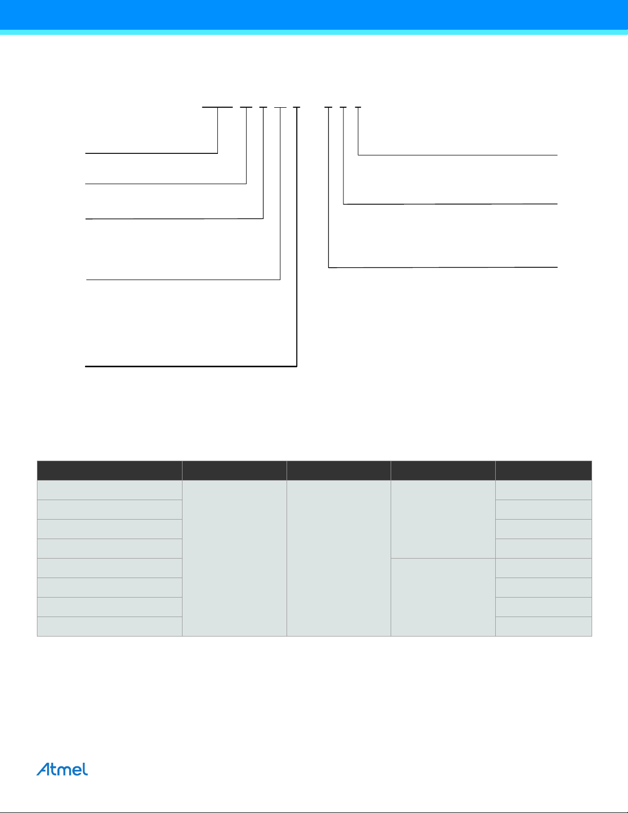
SAMD 21 E 15 A - M U T
Product Family
SAMD = General Purpose Microcontroller
21 = Cortex M0 + CPU, Basic Feature Set
E = 32 Pins
G = 48 Pins
J = 64 Pins
No character = Tray (Default)
T = Tape and Reel
U = -40 - 85
O
C Matte Sn Plating
F = -40 - 125
O
C Matte Sn Plating
A = TQFP
M = QFN
U = WLCSP
C = UFBGA
+ DMA + USB
Product Series
Flash Memory Density
Device Variant
A = Default Variant
B = Added RWW support for 32KB and 64KB memory options
Pin Count
Package Carrier
Package Grade
Package Type
18 = 256KB
17 = 128KB
16 = 64KB
15 = 32KB
2.1 SAM D21E
2.1.1 Device Variant A
Ordering Code FLASH (bytes) SRAM (bytes) Package Carrier Type
ATSAMD21E15A-AU
ATSAMD21E15A-AUT Tape & Reel
ATSAMD21E15A-AF Tray
ATSAMD21E15A-AFT Tape & Reel
ATSAMD21E15A-MU
ATSAMD21E15A-MUT Tape & Reel
ATSAMD21E15A-MF Tray
ATSAMD21E15A-MFT Tape & Reel
32K 4K
TQFP32
QFN32
Tray
Tray
Atmel | SMART SAM D21 [DATASHEET]
Atmel-42181G–SAM-D21_Datasheet–09/2015
5
Page 6

2.1.1 Device Variant A (Continued)
Ordering Code FLASH (bytes) SRAM (bytes) Package Carrier Type
ATSAMD21E16A-AU
Tray
ATSAMD21E16A-AUT Tape & Reel
TQFP32
ATSAMD21E16A-AF Tray
ATSAMD21E16A-AFT Tape & Reel
64K 8K
ATSAMD21E16A-MU
Tray
ATSAMD21E16A-MUT Tape & Reel
QFN32
ATSAMD21E16A-MF Tray
ATSAMD21E16A-MFT Tape & Reel
ATSAMD21E17A-AU
Tray
ATSAMD21E17A-AUT Tape & Reel
TQFP32
ATSAMD21E17A-AF Tray
ATSAMD21E17A-AFT Tape & Reel
128K 16K
ATSAMD21E17A-MU
Tray
ATSAMD21E17A-MUT Tape & Reel
QFN32
ATSAMD21E17A-MF Tray
ATSAMD21E17A-MFT Tape & Reel
ATSAMD21E18A-AU
Tray
ATSAMD21E18A-AUT Tape & Reel
TQFP32
ATSAMD21E18A-AF Tray
ATSAMD21E18A-AFT Tape & Reel
256K 32K
ATSAMD21E18A-MU
Tray
ATSAMD21E18A-MUT Tape & Reel
QFN32
ATSAMD21E18A-MF Tray
ATSAMD21E18A-MFT Tape & Reel
Atmel | SMART SAM D21 [DATASHEET]
Atmel-42181G–SAM-D21_Datasheet–09/2015
6
Page 7

2.1.2 Device Variant B
Ordering Code FLASH (bytes) SRAM (bytes) Package Carrier Type
ATSAMD21E15B-AU
ATSAMD21E15B-AUT Tape & Reel
TQFP32
ATSAMD21E15B-AF Tray
ATSAMD21E15B-AFT Tape & Reel
32K 4K
ATSAMD21E15B-MU
ATSAMD21E15B-MUT Tape & Reel
QFN32
ATSAMD21E15B-MF Tray
ATSAMD21E15B-MFT Tape & Reel
ATSAMD21E15B-UUT 32K 4K WLCSP35 Tape & Reel
ATSAMD21E16B-AU
ATSAMD21E16B-AUT Tape & Reel
TQFP32
ATSAMD21E16B-AF Tray
ATSAMD21E16B-AFT Tape & Reel
64K 8K
ATSAMD21E16B-MU
ATSAMD21E16B-MUT Tape & Reel
QFN32
ATSAMD21E16B-MF Tray
Tray
Tray
Tray
Tray
ATSAMD21E16B-MFT Tape & Reel
ATSAMD21E16B-UUT 64K 8K WLCSP35 Tape & Reel
2.2 SAM D21G
2.2.1 Device Variant A
Ordering Code FLASH (bytes) SRAM (bytes) Package Carrier Type
ATSAMD21G15A-AU
ATSAMD21G15A-AUT Tape & Reel
TQFP48
ATSAMD21G15A-AF Tray
ATSAMD21G15A-AFT Tape & Reel
32K 4K
ATSAMD21G15A-MU
ATSAMD21G15A-MUT Tape & Reel
QFN48
ATSAMD21G15A-MF Tray
ATSAMD21G15A-MFT Tape & Reel
Tray
Tray
Atmel | SMART SAM D21 [DATASHEET]
Atmel-42181G–SAM-D21_Datasheet–09/2015
7
Page 8

2.2.1 Device Variant A (Continued)
Ordering Code FLASH (bytes) SRAM (bytes) Package Carrier Type
ATSAMD21G16A-AU
Tray
ATSAMD21G16A-AUT Tape & Reel
TQFP48
ATSAMD21G16A-AF Tray
ATSAMD21G16A-AFT Tape & Reel
64K 8K
ATSAMD21G16A-MU
Tray
ATSAMD21G16A-MUT Tape & Reel
QFN48
ATSAMD21G16A-MF Tray
ATSAMD21G16A-MFT Tape & Reel
ATSAMD21G17A-AU
Tray
ATSAMD21G17A-AUT Tape & Reel
TQFP48
ATSAMD21G17A-AF Tray
ATSAMD21G17A-AFT Tape & Reel
ATSAMD21G17A-MU
128K 16K
Tray
ATSAMD21G17A-MUT Tape & Reel
QFN48
ATSAMD21G17A-MF Tray
ATSAMD21G17A-MFT Tape & Reel
ATSAMD21G17A-UUT WLCSP45 Tape & Reel
ATSAMD21G18A-AU
Tray
ATSAMD21G18A-AUT Tape & Reel
TQFP48
ATSAMD21G18A-AF Tray
ATSAMD21G18A-AFT Tape & Reel
ATSAMD21G18A-MU
256K 32K
Tray
ATSAMD21G18A-MUT Tape & Reel
QFN48
ATSAMD21G18A-MF Tray
ATSAMD21G18A-MFT Tape & Reel
ATSAMD21G18A-UUT WLCSP45 Tape & Reel
Atmel | SMART SAM D21 [DATASHEET]
Atmel-42181G–SAM-D21_Datasheet–09/2015
8
Page 9

2.2.2 Device Variant B
Ordering Code FLASH (bytes) SRAM (bytes) Package Carrier Type
ATSAMD21G15B-AU
ATSAMD21G15B-AUT Tape & Reel
TQFP48
ATSAMD21G15B-AF Tray
ATSAMD21G15B-AFT Tape & Reel
32K 4K
ATSAMD21G15B-MU
ATSAMD21G15B-MUT Tape & Reel
QFN48
ATSAMD21G15B-MF Tray
ATSAMD21G15B-MFT Tape & Reel
ATSAMD21G16B-AU
ATSAMD21G16B-AUT Tape & Reel
TQFP48
ATSAMD21G16B-AF Tray
ATSAMD21G16B-AFT Tape & Reel
64K 8K
ATSAMD21G16B-MU
ATSAMD21G16B-MUT Tape & Reel
QFN48
ATSAMD21G16B-MF Tray
ATSAMD21G16B-MFT Tape & Reel
Tray
Tray
Tray
Tray
2.3 SAM D21J
2.3.1 Device Variant A
Ordering Code FLASH (bytes) SRAM (bytes) Package Carrier Type
ATSAMD21J15A-AU
ATSAMD21J15A-AUT Tape & Reel
TQFP64
ATSAMD21J15A-AF Tray
ATSAMD21J15A-AFT Tape & Reel
32K 4K
ATSAMD21J15A-MU
ATSAMD21J15A-MUT Tape & Reel
QFN64
ATSAMD21J15A-MF Tray
ATSAMD21J15A-MFT Tape & Reel
Tray
Tray
Atmel | SMART SAM D21 [DATASHEET]
Atmel-42181G–SAM-D21_Datasheet–09/2015
9
Page 10

2.3.1 Device Variant A (Continued)
Ordering Code FLASH (bytes) SRAM (bytes) Package Carrier Type
ATSAMD21J16A-AU
Tray
ATSAMD21J16A-AUT Tape & Reel
TQFP64
ATSAMD21J16A-AF Tray
ATSAMD21J16A-AFT Tape & Reel
ATSAMD21J16A-MU
Tray
64K 8K
ATSAMD21J16A-MUT Tape & Reel
QFN64
ATSAMD21J16A-MF Tray
ATSAMD21J16A-MFT Tape & Reel
ATSAMD21J16A-CU
Tray
UFBGA64
ATSAMD21J16A-CUT Tape & Reel
ATSAMD21J17A-AU
Tray
ATSAMD21J17A-AUT Tape & Reel
TQFP64
ATSAMD21J17A-AF Tray
ATSAMD21J17A-AFT Tape & Reel
ATSAMD21J17A-MU
Tray
128K 16K
ATSAMD21J17A-MUT Tape & Reel
QFN64
ATSAMD21J17A-MF Tray
ATSAMD21J17A-MFT Tape & Reel
ATSAMD21J17A-CU
Tray
UFBGA64
ATSAMD21J17A-CUT Tape & Reel
ATSAMD21J18A-AU
Tray
ATSAMD21J18A-AUT Tape & Reel
TQFP64
ATSAMD21J18A-AF Tray
ATSAMD21J18A-AFT Tape & Reel
ATSAMD21J18A-MU
Tray
256K 32K
ATSAMD21J18A-MUT Tape & Reel
QFN64
ATSAMD21J18A-MF Tray
ATSAMD21J18A-MFT Tape & Reel
ATSAMD21J18A-CU
Tray
UFBGA64
ATSAMD21J18A-CUT Tape & Reel
Atmel | SMART SAM D21 [DATASHEET]
Atmel-42181G–SAM-D21_Datasheet–09/2015
10
Page 11

2.3.2 Device Variant B
Ordering Code FLASH (bytes) SRAM (bytes) Package Carrier Type
ATSAMD21J15B-AU
Tray
ATSAMD21J15B-AUT Tape & Reel
TQFP64
ATSAMD21J15B-AF Tray
ATSAMD21J15B-AFT Tape & Reel
32K 4K
ATSAMD21J15B-MU
Tray
ATSAMD21J15B-MUT Tape & Reel
QFN64
ATSAMD21J15B-MF Tray
ATSAMD21J15B-MFT Tape & Reel
ATSAMD21J16B-AU
Tray
ATSAMD21J16B-AUT Tape & Reel
TQFP64
ATSAMD21J16B-AF Tray
ATSAMD21J16B-AFT Tape & Reel
ATSAMD21J16B-MU
Tray
64K 8K
ATSAMD21J16B-MUT Tape & Reel
QFN64
ATSAMD21J16B-MF Tray
ATSAMD21J16B-MFT Tape & Reel
ATSAMD21J16B-CU
Tray
UFBGA64
ATSAMD21J16B-CUT Tape & Reel
Atmel | SMART SAM D21 [DATASHEET]
Atmel-42181G–SAM-D21_Datasheet–09/2015
11
Page 12
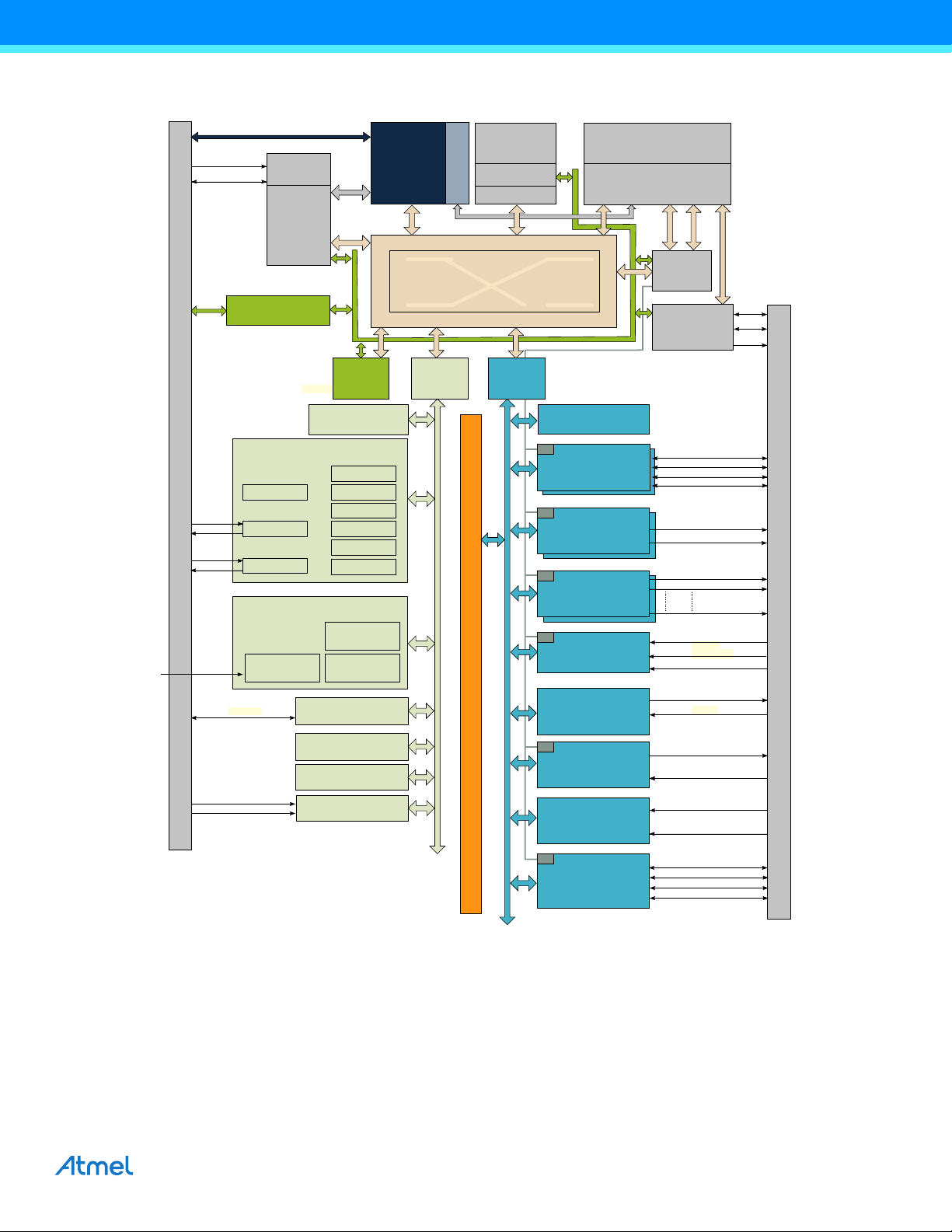
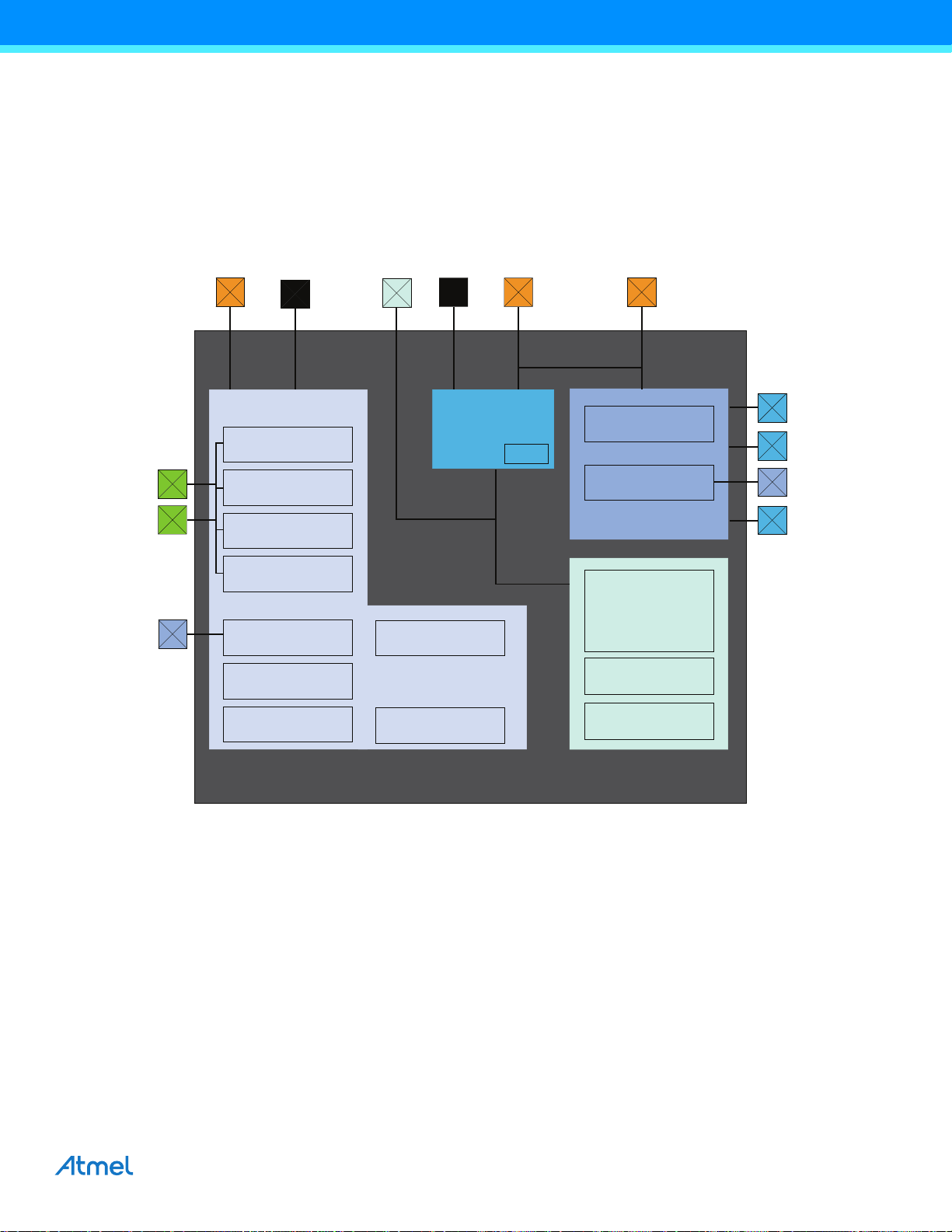
3. Block Diagram
6 x SERCOM
8 x Timer Counter
REAL TIME
COUNTER
AHB-APB
BRIDGE C
M
M
HIGH SPEED
BUS MATRIX
PORT
PORT
WATCHDOG
TIMER
SERIAL
WIRE
SWDIO
S
CORTEX-M0+
PROCESSOR
Fmax 48 MHz
SWCLK
DEVICE
SERVICE
UNIT
AHB-APB
BRIDGE A
20-CHANNEL
12-bit ADC 350KSPS
AIN[19..0]
VREFA
AIN[3..0]
S
SRAM
CONTROLLER
32/16/8/4KB
RAM
M
RESET
CONTROLLER
SLEEP
CONTROLLER
CLOCK
CONTROLLER
POWER MANAGER
RESETN
5 x TIMER / COUNTER
EVENT SYSTEM
S
6 x SERCOM
2 ANALOG
COMPARATORS
SYSTEM CONTROLLER
XOUT
XIN
XOUT32
XIN32
OSCULP32K
OSC32K
OSC8M
DFLL48M
BOD33
XOSC32K
XOSC
VREF
X[15..0]
Y[15..0]
PERIPHERAL
TOUCH
CONTROLLER
PERIPHERAL
ACCESS CONTROLLER
AHB-APB
BRIDGE B
VREFA
VOUT
10-bit DAC
EXTERNAL INTERRUPT
CONTROLLER
PERIPHERAL
ACCESS CONTROLLER
PERIPHERAL
ACCESS CONTROLLER
EXTINT[15..0]
NMI
GCLK_IO[7..0]
S
PAD0
WO1
PAD1
PAD2
PAD3
WO0
VREFB
256/128/64/32KB
NVM
NVM
CONTROLLER
Cache
S
DMA
USB FS
DEVICE
MINI-HOST
DP
DM
3x TIMER / COUNTER
FOR CONTROL
WOn
IOBUS
FDPLL96M
DMA
DMA
DMA
DMA
DMA
MCK[1..0]
SCK[1..0]
INTER-IC
SOUND
CONTROLLER
SD[1..0]
FS[1..0]
DMA
MICRO
TRACE BUFFER
SOF 1KHZ
WO0
WO1
(2)
GENERIC CLOCK
CONTROLLER
CMP[1..0]
1. Some products have different number of SERCOM instances, Timer/Counter instances, PTC signals and ADC sig-
2. The three TCC instances have different configurations, including the number of Waveform Output (WO) lines. Refer
nals. Refer to “Peripherals Configuration Summary” on page 48 for details.
to Table 30-1 on page 651 for details.
Atmel | SMART SAM D21 [DATASHEET]
Atmel-42181G–SAM-D21_Datasheet–09/2015
12
Page 13

4. Pinout
PA00
1
PA01
2
PA02
3
PA03
4
PB04
5
PB05
6
GNDANA
7
VDDANA
8
PB06
9
PB07
10
PB08
11
PB09
12
PA04
13
PA05
14
PA06
15
PA07
16
PA08
17
PA09
18
PA10
19
PA11
20
VDDIO
21
GND
22
PB10
23
PB11
24
PB12
25
PB13
26
PB14
27
PB15
28
PA12
29
PA13
30
PA14
31
PA15
32
VDDIO48
GND47
PA2546
PA2445
PA2344
PA2243
PA2142
PA2041
PB1740
PB1639
PA1938
PA1837
PA1736
PA1635
VDDIO34
GND33
PB22
49
PB23
50
PA27
51
RESETN
52
PA28
53
GND
54
VDDCORE
55
VDDIN
56
PA30
57
PA31
58
PB30
59
PB31
60
PB00
61
PB01
62
PB02
63
PB03
64
DIGITAL PIN
ANALOG PIN
OSCILLATOR
GROUND
INPUT SUPPLY
REGULATED OUTPUT SUPPLY
RESET PIN
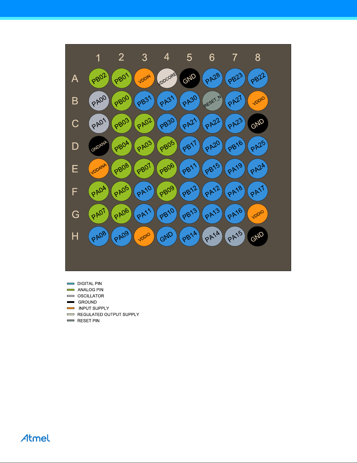
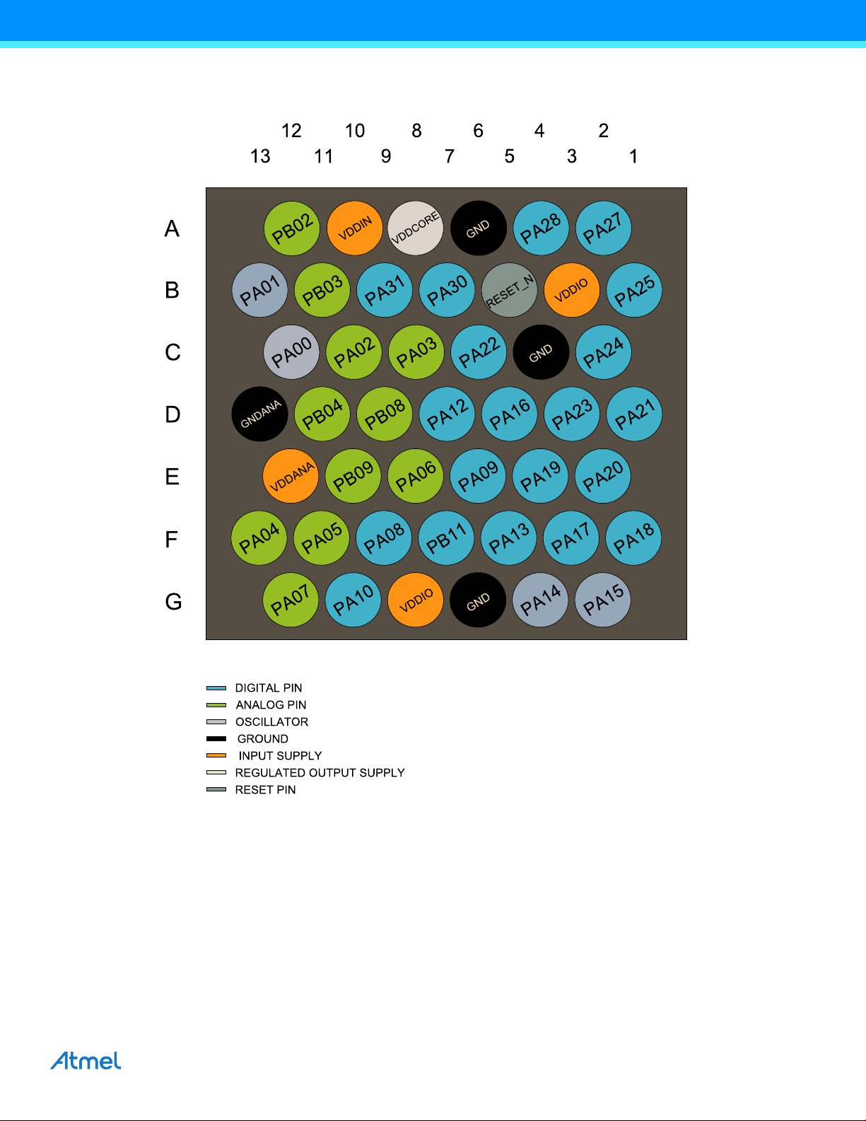
4.1 SAM D21J
4.1.1 QFN64 / TQFP64
Atmel | SMART SAM D21 [DATASHEET]
Atmel-42181G–SAM-D21_Datasheet–09/2015
13
Page 14
4.1.2 UFBGA64
Atmel | SMART SAM D21 [DATASHEET]
Atmel-42181G–SAM-D21_Datasheet–09/2015
14
Page 15
4.2 SAM D21G
PA21
PA00
1
PA01
2
PA02
3
PA03
4
GNDANA
5
VDDANA
6
PB08
7
PB09
8
PA04
9
PA05
10
PA06
11
PA07
12
PA08
13
PA09
14
PA10
15
PA11
16
VDDIO
17
GND
18
PB10
19
PB11
20
PA12 21
PA13
22
PA14
23
PA15
24
VDDIO36
GND35
PA2534
PA2433
PA2332
PA2231
30
PA2029
PA1928
PA1827
PA1726
PA1625
PB22
37
PB23
38
PA27
39
RESETN
40
PA28
41
GND
42
VDDCORE
43
VDDIN
44
PA30
45
PA31
46
PB02
47
PB03
48
DIGITAL PIN
ANALOG PIN
OSCILLATOR
GROUND
INPUT SUPPLY
REGULATED OUTPUT SUPPLY
RESET PIN
4.2.1 QFN48 / TQFP48
Atmel | SMART SAM D21 [DATASHEET]
Atmel-42181G–SAM-D21_Datasheet–09/2015
15
Page 16
4.2.2 WLCSP45
Atmel | SMART SAM D21 [DATASHEET]
Atmel-42181G–SAM-D21_Datasheet–09/2015
16
Page 17
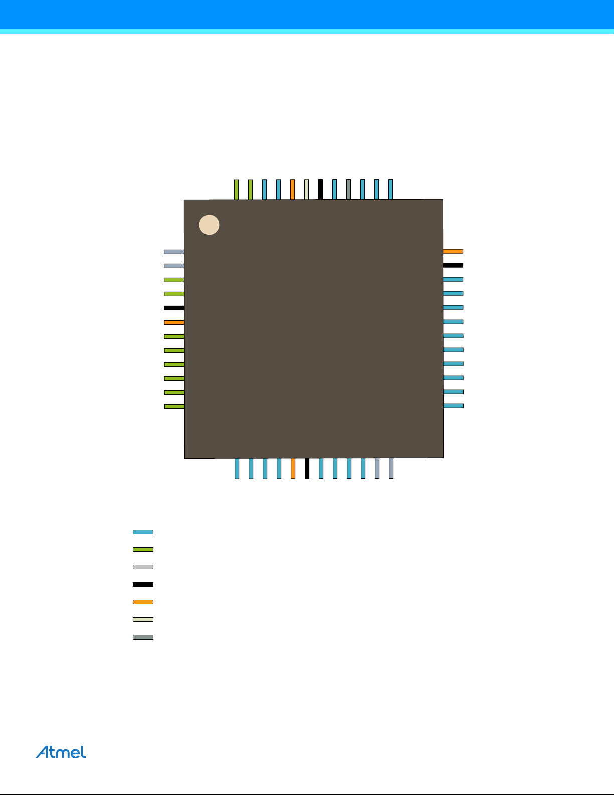
4.3 SAM D21E
PA00
1
PA01
2
PA02
3
PA03
4
PA04
5
PA05
6
PA06
7
PA07
8
VDDANA
9
GND
10
PA08
11
PA09
12
PA10
13
PA11
14
PA14
15
PA15
16
PA25
24
PA24
23
PA23
22
PA22
21
PA19
20
PA18
19
PA17
18
PA16
17
PA27
25
RESETN
26
PA28
27
GND
28
VDDCORE
29
VDDIN
30
PA30
31
PA31
32
DIGITAL PIN
ANALOG PIN
OSCILLATOR
GROUND
INPUT SUPPLY
REGULATED OUTPUT SUPPLY
RESET PIN
4.3.1 QFN32 / TQFP32
Atmel | SMART SAM D21 [DATASHEET]
Atmel-42181G–SAM-D21_Datasheet–09/2015
17
Page 18
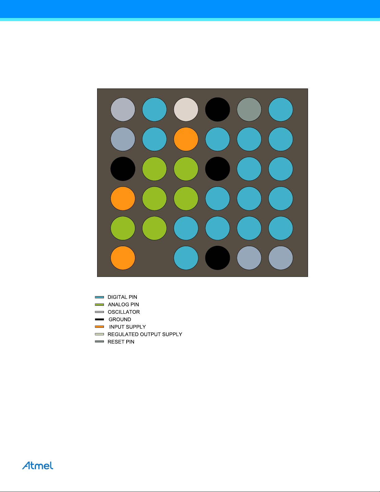
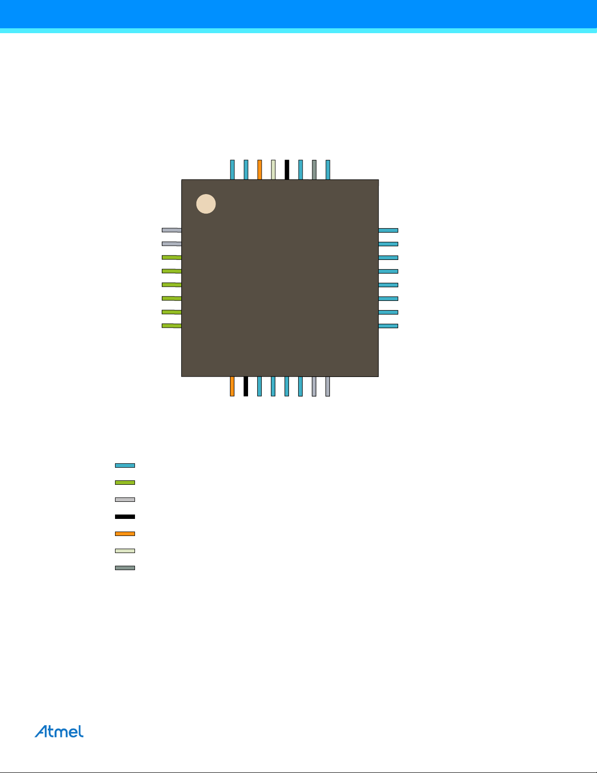
4.3.2 WLCSP35
PA00
PA01
GNDANA
VDDANA
PA06
VDDIO
PA15
PA18
PA19
PA23
PA24
PA25
PA14
PA16
PA17
PA22
PA27
RESET_N
PA03
PA05
PA10
PA08
VDDIN
VDDCORE
PA02
PA04
PA07
PA31
PA30
PA11
PA09
PA28
GND
GND
GND
1
2
3
4
5
6
ABCDEF
Atmel | SMART SAM D21 [DATASHEET]
Atmel-42181G–SAM-D21_Datasheet–09/2015
18
Page 19

5. Signal Descriptions List
The following table gives details on signal names classified by peripheral.
Signal Name Function Type Active Level
Analog Comparators - AC
AIN[3:0] AC Analog Inputs Analog
CMP[:0] AC Comparator Outputs Digital
Analog Digital Converter - ADC
AIN[19:0] ADC Analog Inputs Analog
VREFA ADC Voltage External Reference A Analog
VREFB ADC Voltage External Reference B Analog
Digital Analog Converter - DAC
VOUT DAC Voltage output Analog
VREFA DAC Voltage External Reference Analog
External Interrupt Controller
EXTINT[15:0] External Interrupts Input
NMI External Non-Maskable Interrupt Input
Generic Clock Generator - GCLK
GCLK_IO[7:0] Generic Clock (source clock or generic clock generator output) I/O
Inter-IC Sound Controller - I2S
MCK[1..0] Master Clock I/O
SCK[1..0] Serial Clock I/O
FS[1..0] I2S Word Select or TDM Frame Sync I/O
SD[1..0] Serial Data Input or Output I/O
Power Manager - PM
RESETN Reset Input Low
Serial Communication Interface - SERCOMx
PAD[3:0] SERCOM I/O Pads I/O
System Control - SYSCTRL
XIN Crystal Input Analog/ Digital
XIN32 32kHz Crystal Input Analog/ Digital
XOUT Crystal Output Analog
XOUT32 32kHz Crystal Output Analog
Timer Counter - TCx
Atmel | SMART SAM D21 [DATASHEET]
Atmel-42181G–SAM-D21_Datasheet–09/2015
19
Page 20

Signal Name Function Type Active Level
WO[1:0] Waveform Outputs Output
Timer Counter - TCCx
WO[1:0] Waveform Outputs Output
Peripheral Touch Controller - PTC
X[15:0] PTC Input Analog
Y[15:0] PTC Input Analog
General Purpose I/O - PORT
PA25 - PA00 Parallel I/O Controller I/O Port A I/O
PA28 - PA27 Parallel I/O Controller I/O Port A I/O
PA31 - PA30 Parallel I/O Controller I/O Port A I/O
PB17 - PB00 Parallel I/O Controller I/O Port B I/O
PB23 - PB22 Parallel I/O Controller I/O Port B I/O
PB31 - PB30 Parallel I/O Controller I/O Port B I/O
Universal Serial Bus - USB
DP DP for USB I/O
DM DM for USB I/O
SOF 1kHz USB Start of Frame I/O
Atmel | SMART SAM D21 [DATASHEET]
Atmel-42181G–SAM-D21_Datasheet–09/2015
20
Page 21

Atmel-42181G–SAM-D21_Datasheet–09/2015
[DATASHEET]
21
6. I/O Multiplexing and Considerations
6.1 Multiplexed Signals
Each pin is by default controlled by the PORT as a general purpose I/O and alternatively it can be assigned to one of the peripheral functions A, B, C,
D, E, F, G or H. To enable a peripheral function on a pin, the Peripheral Multiplexer Enable bit in the Pin Configuration register corresponding to that pin
(PINCFGn.PMUXEN, n = 0-31) in the PORT must be written to one. The selection of peripheral function A to H is done by writing to the Peripheral
Multiplexing Odd and Even bits in the Peripheral Multiplexing register (PMUXn.PMUXE/O) in the PORT.
Table 5-1 on page 11 describes the peripheral signals multiplexed to the PORT I/O pins.
Table 6-1. PORT Function Multiplexing
(1)
Pin
SAMD21E SAMD21GSAMD21J EIC REF ADC AC PTC DAC SERCOM
1 1 1 PA0 0 VDDANA EXTINT[0]
2 2 2 PA0 1 VDDANA EXTINT[1]
3 3 3 PA02 VDDANA EXTINT[2] AIN[0] Y[0] VOUT
4 4 4 PA03 VDDANA EXTINT[3]
7 11 PB08 VDDANA EXTINT[8] AIN[2] Y[14]
8 12 PB09 VDDANA EXTINT[9] AIN[3] Y[15]
5 9 13 PA0 4 VDDANA EXTINT[4]
6 10 14 PA 05 VDDANA EXTINT[5] AIN[5] AIN[1] Y[3]
7 11 15 PA 06 VDDANA EXTINT[6] AIN[6] AIN[2] Y[4]
8 12 16 PA 07 VDDANA EXTINT[7] AIN[7] AIN[3] Y[5]
11 13 17 PA 08 VDDIO I2C NMI AIN[16] X[0]
12 14 18 PA0 9 VDDIO I2C EXTINT[9] AIN[17] X[1]
13 15 19 PA1 0 VDDIO EXTINT[10] AIN[18] X[2]
14 16 20 PA11 VDDIO EXTINT[11] AIN[19] X[3]
I/O Pin Supply Typ e
5 PB04 VDDANA EXTINT[4] AIN[12] Y[10]
6 PB05 VDDANA EXTINT[5] AIN[13] Y[11]
9 PB06 VDDANA EXTINT[6] AIN[14] Y[12]
10 PB07 VDDANA EXTINT[7] AIN[15] Y[13]
A B
ADC/VREFA
DAC/VREFA
ADC/VREFB
(2)(3)
AIN[1] Y[1]
AIN[4] AIN[0] Y[2]
C D E F G H
SERCOM0/
PAD [0]
SERCOM0/
PAD [1]
SERCOM0/
PAD [2]
SERCOM0/
PAD [3]
(2)(3)
SERCOM-
ALT
SERCOM1/
PAD [0]
SERCOM1/
PAD [1]
SERCOM4/
PAD [0]
SERCOM4/
PAD [1]
SERCOM0/
PAD [0]
SERCOM0/
PAD [1]
SERCOM0/
PAD [2]
SERCOM0/
PAD [3]
SERCOM2/
PAD [0]
SERCOM2/
PAD [1]
SERCOM2/
PAD [2]
SERCOM2/
PAD [3]
(4)
TC
/TCC TCC COM AC/GCLK
TCC2/WO[0]
TCC2/WO[1]
TC4/WO[0]
TC4/WO[1]
TCC0/WO[0]
TCC0/WO[1]
TCC1/WO[0]
TCC1/WO[1] I2S/SD[0]
TCC0/WO[0]
TCC0/WO[1]
TCC1/WO[0]
TCC1/WO[1]
TCC1/
WO[2]
TCC1/
WO[3]
TCC0/
WO[2]
TCC0/
WO[3]
I2S/SD[1]
I2S/
MCK[0]
I2S/
SCK[0]
I2S/FS[0] GCLK_IO[5]
GCLK_IO[4]
Page 22

Atmel-42181G–SAM-D21_Datasheet–09/2015
[DATASHEET]
22
Table 6-1. PORT Function Multiplexing (Continued)
(1)
Pin
SAMD21E SAMD21GSAMD21J EIC REF ADC AC PTC DAC SERCOM
19 23 PB10 VDDIO EXTINT[10]
20 24 PB11 VDDIO EXTINT[11]
21 29 PA 12 VDDIO I2C EXTINT[12]
22 30 PA 13 VDDIO I2C EXTINT[13]
15 23 31 PA1 4 VDDIO EXTINT[14]
16 24 32 PA1 5 VDDIO EXTINT[15]
17 25 35 PA1 6 VDDIO I2C EXTINT[0] X[4]
18 26 36 PA1 7 VDDIO I2C EXTINT[1] X[5]
19 27 37 PA1 8 VDDIO EXTINT[2] X[6]
20 28 38 PA1 9 VDDIO EXTINT[3] X[7]
29 41 PA 20 VDDIO EXTINT[4] X[8]
30 42 PA 21 VDDIO EXTINT[5] X[9]
21 31 43 PA2 2 VDDIO I2C EXTINT[6] X[10]
22 32 44 PA2 3 VDDIO I2C EXTINT[7] X[11]
23 33 45 PA2 4 VDDIO EXTINT[12]
24 34 46 PA2 5 VDDIO EXTINT[13]
I/O Pin Supply Typ e
25 PB12 VDDIO I2C EXTINT[12] X[12]
26 PB13 VDDIO I2C EXTINT[13] X[13]
27 PB14 VDDIO EXTINT[14] X[14]
28 PB15 VDDIO EXTINT[15] X[15]
39 PB16 VDDIO I2C EXTINT[0]
40 PB17 VDDIO I2C EXTINT[1]
A B
(2)(3)
C D E F G H
SERCOM4/
PAD [0]
SERCOM4/
PAD [1]
SERCOM4/
PAD [2]
SERCOM4/
PAD [3]
SERCOM2/
PAD [0]
SERCOM2/
PAD [1]
SERCOM2/
PAD [2]
SERCOM2/
PAD [3]
SERCOM1/
PAD [0]
SERCOM1/
PAD [1]
SERCOM1/
PAD [2]
SERCOM1/
PAD [3]
SERCOM5/
PAD [0]
SERCOM5/
PAD [1]
SERCOM5/
PAD [2]
SERCOM5/
PAD [3]
SERCOM3/
PAD [0]
SERCOM3/
PAD [1]
SERCOM3/
PAD [2]
SERCOM3/
PAD [3]
(2)(3)
SERCOM-
ALT
SERCOM4/
PAD [2]
SERCOM4/
PAD [3]
SERCOM4/
PAD [0]
SERCOM4/
PAD [1]
SERCOM4/
PAD [2]
SERCOM4/
PAD [3]
SERCOM3/
PAD [0]
SERCOM3/
PAD [1]
SERCOM3/
PAD [2]
SERCOM3/
PAD [3]
SERCOM3/
PAD [2]
SERCOM3/
PAD [3]
SERCOM5/
PAD [0]
SERCOM5/
PAD [1]
SERCOM5/
PAD [2]
SERCOM5/
PAD [3]
(4)
TC
/TCC TCC COM AC/GCLK
TC5/WO[0]
TC5/WO[1]
TC4/WO[0]
TC4/WO[1]
TC5/WO[0] GCLK_IO[0]
TC5/WO[1] GCLK_IO[1]
TCC2/WO[0]
TCC2/WO[1]
TC3/WO[0]
TC3/WO[1]
TCC2/WO[0] TCC0/WO[6] GCLK_IO[2]
TCC2/WO[1] TCC0/WO[7] GCLK_IO[3]
TC3/WO[0]
TC3/WO[1]
TC6/WO[0]
TC6/WO[1]
TC7/WO[0]
TC7/WO[1]
TC4/WO[0]
TC4/WO[1]
TC5/WO[0]
TC5/WO[1]
TCC0/
WO[4]
TCC0/
WO[5]
TCC0/
WO[6]
TCC0/
WO[7]
TCC0/
WO[6]
TCC0/
WO[7]
TCC0/
WO[4]
TCC0/
WO[5]
TCC0/
WO[2]
TCC0/
WO[3]
TCC0/
WO[4]
TCC0/
WO[5]
TCC0/
WO[6]
TCC0/
WO[7]
TCC0/
WO[4]
TCC0/
WO[5]
TCC1/
WO[2]
TCC1/
WO[3]
I2S/
I2S/
I2S/
I2S/
1kHz
GCLK_IO[4]
GCLK_IO[5]
GCLK_IO[7]
AC/CMP[0]
AC/CMP[1]
GCLK_IO[0]
GCLK_IO[1]
AC/CMP[0]
GCLK_IO[3]
GCLK_IO[4]
GCLK_IO[6]
GCLK_IO[7]
MCK[1]
SCK[1]
I2S/FS[1] GCLK_IO[6]
I2S/SD[0] AC/CMP[1]
I2S/SD[1] GCLK_IO[2]
MCK[0]
SCK[0]
I2S/FS[0] GCLK_IO[5]
USB/SOF
USB/DM
USB/DP
Page 23

Table 6-1. PORT Function Multiplexing (Continued)
(1)
Pin
SAMD21E SAMD21GSAMD21J EIC REF ADC AC PTC DAC SERCOM
37 49 PB22 VDDIO EXTINT[6]
38 50 PB23 VDDIO EXTINT[7]
25 39 51 PA2 7 VDDIO EXTINT[15] GCLK_IO[0]
27 41 53 PA2 8 VDDIO EXTINT[8] GCLK_IO[0]
31 45 57 PA3 0 VDDIO EXTINT[10]
32 46 58 PA3 1 VDDIO EXTINT[11]
47 63 PB02 VDDANA EXTINT[2] AIN[10] Y[8]
48 64 PB03 VDDANA EXTINT[3] AIN[11] Y[9]
Notes: 1. Use the SAMD21J pinout muxing for WLCSP45 package.
2. All analog pin functions are on peripheral function B. Peripheral function B must be selected to disable the digital control of the pin.
3. Only some pins can be used in SERCOM I
characteristics.
4. Note that TC6 and TC7 are not supported on the SAM D21E and G devices. Refer to “Configuration Summary” on page 3 for details.
5. This function is only activated in the presence of a debugger.
I/O Pin Supply Typ e
59 PB30 VDDIO I2C EXTINT[14]
60 PB31 VDDIO I2C EXTINT[15]
61 PB00 VDDANA EXTINT[0] AIN[8] Y[6]
62 PB01 VDDANA EXTINT[1] AIN[9] Y[7]
2
C mode. See the Type column for using a SERCOM pin in I2C mode. Refer to “Electrical Characteristics” on page 935 for details on the I2C pin
A B
(2)(3)
C D E F G H
SERCOM-
(2)(3)
ALT
SERCOM5/
PAD [2]
SERCOM5/
PAD [3]
SERCOM1/
PAD [2]
SERCOM1/
PAD [3]
SERCOM5/
PAD [0]
SERCOM5/
PAD [1]
SERCOM5/
PAD [2]
SERCOM5/
PAD [3]
SERCOM5/
PAD [0]
SERCOM5/
PAD [1]
(4)
TC
/TCC TCC COM AC/GCLK
TC7/WO[0] GCLK_IO[0]
TC7/WO[1] GCLK_IO[1]
TCC1/WO[0] SWCLK GCLK_IO[0]
TCC1/WO[1] SWDIO
TCC0/WO[0]
TCC0/WO[1]
TC7/WO[0]
TC7/WO[1]
TC6/WO[0]
TC6/WO[1]
TCC1/
WO[2]
TCC1/
WO[3]
(5)
Atmel-42181G–SAM-D21_Datasheet–09/2015
[DATASHEET]
23
Page 24

6.2 Other Functions
6.2.1 Oscillator Pinout
The oscillators are not mapped to the normal PORT functions and their multiplexing are controlled by registers in the
System Controller (SYSCTRL).
Oscillator Supply Signal I/O Pin
XOSC VDDIO
XOSC32K VDDANA
6.2.2 Serial Wire Debug Interface Pinout
Only the SWCLK pin is mapped to the normal PORT functions. A debugger cold-plugging or hot-plugging detection will
automatically switch the SWDIO port to the SWDIO function.
Signal Supply I/O Pin
SWCLK VDDIO PA30
SWDIO VDDIO PA31
XIN PA1 4
XOUT PA1 5
XIN32 PA0 0
XOUT32 PA01
Atmel | SMART SAM D21 [DATASHEET]
Atmel-42181G–SAM-D21_Datasheet–09/2015
24
Page 25
7. Power Supply and Start-Up Considerations
VOLTAGE
REGULATOR
VDDIN
VDDCORE
GND
ADC
AC
DAC
PTC
XOSC32K
OSC32K
VDDANA
GNDANA
PA[7:2]
PB[9:0]
PA[1:0]
Digital Logic
(CPU, peripherals)
DFLL48M
VDDIO
OSC8M
XOSC
OSCULP32K
PA[31:16]
PB[31:10]
PA[15:14]
BOD33
POR
PA[13:8]
BOD12
FDPLL96M
7.1 Power Domain Overview
7.2 Power Supply Considerations
7.2.1 Power Supplies
The Atmel® SAM D21 has several different power supply pins:
z VDDIO: Powers I/O lines, OSC8M and XOSC. Voltage is 1.62V to 3.63V.
z VDDIN: Powers I/O lines and the internal regulator. Voltage is 1.62V to 3.63V.
z VDDANA: Powers I/O lines and the ADC, AC, DAC, PTC, OSCULP32K, OSC32K, XOSC32K. Voltage is 1.62V to
3.63V.
z VDDCORE: Internal regulated voltage output. Powers the core, memories, peripherals, DFLL48M and
FDPLL96M. Voltage is 1.2V.
The same voltage must be applied to both VDDIN, VDDIO and VDDANA. This common voltage is referred to as V
the datasheet.
DD
in
Atmel | SMART SAM D21 [DATASHEET]
Atmel-42181G–SAM-D21_Datasheet–09/2015
25
Page 26
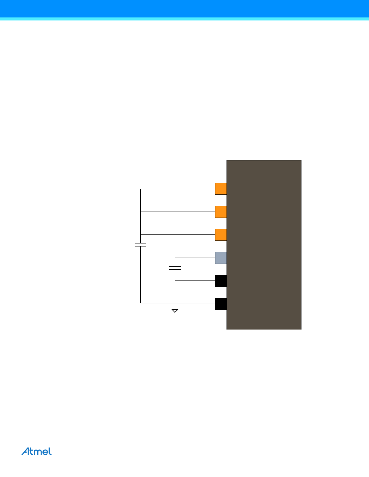
The ground pins, GND, are common to VDDCORE, VDDIO and VDDIN. The ground pin for VDDANA is GNDANA.
(1.62V — 3.63V)
Main Supply
VDDIO
VDDANA
VDDIN
VDDCORE
GND
GNDANA
SAM D21
For decoupling recommendations for the different power supplies, refer to the schematic checklist.
Refer to “Schematic Checklist” on page 1008 for details.
7.2.2 Voltage Regulator
The SAM D21 voltage regulator has two different modes:
z Normal mode: To be used when the CPU and peripherals are running
z Low Power (LP) mode: To be used when the regulator draws small static current. It can be used in standby mode
7.2.3 Typical Powering Schematics
The SAM D21 uses a single supply from 1.62V to 3.63V.
The following figure shows the recommended power supply connection.
Figure 7-1. Power Supply Connection
7.2.4 Power-Up Sequence
7.2.4.1 Minimum Rise Rate
7.2.4.2 Maximum Rise Rate
The integrated power-on reset (POR) circuitry monitoring the VDDANA power supply requires a minimum rise rate. Refer
to the “Electrical Characteristics” on page 935 for details.
The rise rate of the power supply must not exceed the values described in Electrical Characteristics. Refer to the
“Electrical Characteristics” on page 935 for details.
Atmel | SMART SAM D21 [DATASHEET]
Atmel-42181G–SAM-D21_Datasheet–09/2015
26
Page 27

7.3 Power-Up
This section summarizes the power-up sequence of the SAM D21. The behavior after power-up is controlled by the
Power Manager. Refer to “PM – Power Manager” on page 117 for details.
7.3.1 Starting of Clocks
After power-up, the device is set to its initial state and kept in reset, until the power has stabilized throughout the device.
Once the power has stabilized, the device will use a 1MHz clock. This clock is derived from the 8MHz Internal Oscillator
(OSC8M), which is divided by eight and used as a clock source for generic clock generator 0. Generic clock generator 0
is the main clock for the Power Manager (PM).
Some synchronous system clocks are active, allowing software execution.
Refer to the “Clock Mask Register” section in “PM – Power Manager” on page 117 for the list of default peripheral clocks
running. Synchronous system clocks that are running are by default not divided and receive a 1MHz clock through
generic clock generator 0. Other generic clocks are disabled except GCLK_WDT, which is used by the Watchdog Timer
(WDT).
7.3.2 I/O Pins
After power-up, the I/O pins are tri-stated.
7.3.3 Fetching of Initial Instructions
After reset has been released, the CPU starts fetching PC and SP values from the reset address, which is 0x00000000.
This address points to the first executable address in the internal flash. The code read from the internal flash is free to
configure the clock system and clock sources. Refer to “PM – Power Manager” on page 117, “GCLK – Generic Clock
Controller” on page 95 and “SYSCTRL – System Controller” on page 148 for details. Refer to the ARM Architecture
Reference Manual for more information on CPU startup (http://www.arm.com).
7.4 Power-On Reset and Brown-Out Detector
The SAM D21 embeds three features to monitor, warn and/or reset the device:
z POR: Power-on reset on VDDANA
z BOD33: Brown-out detector on VDDANA
z BOD12: Voltage Regulator Internal Brown-out detector on VDDCORE. The Voltage Regulator Internal BOD is
calibrated in production and its calibration configuration is stored in the NVM User Row. This configuration should
not be changed if the user row is written to assure the correct behavior of the BOD12.
7.4.1 Power-On Reset on VDDANA
POR monitors VDDANA. It is always activated and monitors voltage at startup and also during all the sleep modes. If
VDDANA goes below the threshold voltage, the entire chip is reset.
7.4.2 Brown-Out Detector on VDDANA
BOD33 monitors VDDANA. Refer to “SYSCTRL – System Controller” on page 148 for details.
7.4.3 Brown-Out Detector on VDDCORE
Once the device has started up, BOD12 monitors the internal VDDCORE.
Atmel | SMART SAM D21 [DATASHEET]
Atmel-42181G–SAM-D21_Datasheet–09/2015
27
Page 28

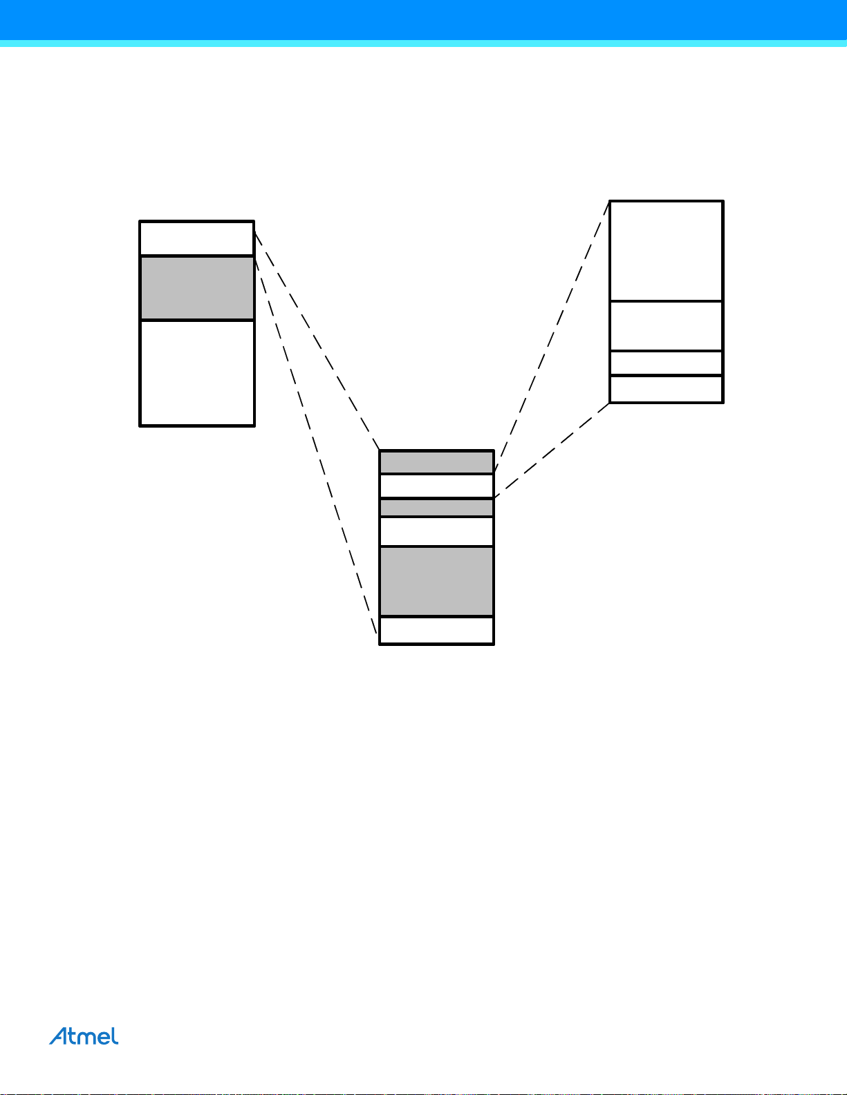
8. Product Mapping
Code
SRAM
Undefined
Peripherals
Reserved
Undefined
Global Memory Space
0x00000000
0x20000000
0x20008000
0x40000000
0x43000000
0x60000000
Internal SRAM
SRAM
AHB-APB
Bridge A
AHB-APB
Bridge B
AHB-APB
Bridge C
AHB-APB
Internal Flash
Reserved
Code
0x00000000
0x00040000
0x1FFFFFFF
0x20000000
0x20007FFF
0x40000000
0x41000000
0x42000000
0x42FFFFFF
Reserved
PAC0
PM
SYSCTRL
GCLK
WDT
RTC
EIC
AHB-APB Bridge A
0x40000000
0x40000400
0x40000800
0x40000C00
0x40001000
0x40001400
0x40001800
0x40FFFFFF
0x40001C00
AHB-APB Bridge B
Reserved
PAC1
DSU
NVMCTRL
PORT
0x41000000
0x41002000
0x41004000
0x41004400
0x41FFFFFF
0x41007000
SERCOM5
PAC2
EVSYS
SERCOM0
SERCOM1
SERCOM2
SERCOM3
SERCOM4
AHB-APB Bridge C
TC7
TCC0
TCC1
TCC2
TC3
TC4
TC5
TC6
ADC
AC
0x42000000
0x42000400
0x42000800
0x42000C00
0x42001000
0x42001400
0x42001800
0x42002000
0x42001C00
0x42003000
0x42003400
0x42003800
0x42003C00
0x42004000
0x42004400
0x42004800
Reserved
0x42FFFFFF
0x60000200
0xFFFFFFFF
Reserved
System
0xE0000000
DAC
0x42004C00
0x42002400
0x42002800
0x42002C00
PTC
0x42005400
0x42005000
I2S
DMAC
USB
MTB
0x41004800
0x41005000
0x41006000
0xE0000000
0xE000E000
0xE000F000
0xE00FF000
0xE0100000
0xFFFFFFFF
System
Reserved
SCS
Reserved
ROMTable
Reserved
Internal Flash
0x00000000
0x00400000
0x1FFFFFFF
Internal
RWW section
Device Variant A
Device Variant B
Figure 8-1. Atmel | SMART SAM D21 Product Mapping
This figure represents the full configuration of the Atmel® SAM D21 with maximum flash and SRAM capabilities and a full
set of peripherals. Refer to the “Configuration Summary” on page 3 for details.
Atmel | SMART SAM D21 [DATASHEET]
Atmel-42181G–SAM-D21_Datasheet–09/2015
28
Page 29

9. Memories
9.1 Embedded Memories
z Internal high-speed flash with Read-While-Write (RWW) capability on section of the array (Device Variant B).
z Internal high-speed flash
z Internal high-speed RAM, single-cycle access at full speed
9.2 Physical Memory Map
The High-Speed bus is implemented as a bus matrix. All High-Speed bus addresses are fixed, and they are never
remapped in any way, even during boot. The 32-bit physical address space is mapped as follow:
Table 9-1. SAM D21 physical memory map
Memory Start address
Internal Flash 0x00000000 256Kbytes 128Kbytes 64Kbytes 32Kbytes
Internal RWW section
Internal SRAM 0x20000000 32Kbytes 16Kbytes 8Kbytes 4Kbytes
Peripheral Bridge A 0x40000000 64Kbytes 64Kbytes 64Kbytes 64Kbytes
Peripheral Bridge B 0x41000000 64Kbytes 64Kbytes 64Kbytes 64Kbytes
Peripheral Bridge C 0x42000000 64Kbytes 64Kbytes 64Kbytes 64Kbytes
(2)
0x00010000 - - 2Kbytes 1Kbytes
(1)
Size
SAMD21x18 SAMD21x17 SAMD21x16 SAMD21x15
Notes: 1. x = G, J or E. Refer to “Ordering Information” on page 5 for details.
2. Only applicable for Device Variant B.
Table 9-2. Flash memory parameters
Device Flash size Number of pages Page size
SAMD21x18 256Kbytes 4096 64 bytes
SAMD21x17 128Kbytes 2046 64 bytes
(1)
SAMD21x16 64Kbytes 1024 64 bytes
SAMD21x15 32Kbytes 512 64 bytes
Note: 1. x = G, J or E. Refer to “Ordering Information” on page 5 for details.
2. The number of pages (NVMP) and page size (PSZ) can be read from the NVM Pages and Page Size bits in
the NVM Parameter register in the NVMCTRL (PARAM.NVMP and PARAM.PSZ, respectively). Refer to
PARAM for details.
Table 9-3. RWW section parameters
Device Flash size Number of pages Page size
SAMD21x16B 2Kbytes 32 64 bytes
SAMD21x15B 1Kbytes 16 64 bytes
Atmel | SMART SAM D21 [DATASHEET]
Atmel-42181G–SAM-D21_Datasheet–09/2015
29
Page 30
9.3 NVM Calibration and Auxiliary Space
0x00800000
AUX0 offset address
Automatic calibration
row
Calibration and auxiliary
space address offset
AUX0 – NVM User
Row
AUX1
0x00804000
0x00806000
AUX1 offset address
0x00806000
Area 3 offset ad
Area 1: Reserved (64 bits)
Area 2: Device configuration
area (64 bits)
Area 1 address
Area 2 offset ad
Area 3: Reserved
(128bits)
Area 4: Software
calibration area (256bits)
0x00806008
0x00806010
0x00806020
Area 4 offset add
AUX1
0x00806040
000000
NVM base address
+ NVM size
NVM main address
space
NVM Base Address
Calibration and
auxiliary space
NVM base address +
0x00800000
The device calibration data are stored in different sections of the NVM calibration and auxiliary space presented in Figure
9-1.
Figure 9-1. Calibration and Auxiliary Space
The values from the automatic calibration row are loaded into their respective registers at startup.
9.3.1 NVM User Row Mapping
The NVM User Row contains calibration data that are automatically read at device power on.
The NVM User Row can be read at address 0x804000.
To write the NVM User Row refer to “NVMCTRL – Non-Volatile Memory Controller” on page 355.
Note that when writing to the user row the values do not get loaded by the other modules on the device until a device
reset occurs.
Atmel | SMART SAM D21 [DATASHEET]
30
Atmel-42181G–SAM-D21_Datasheet–09/2015
Page 31

Table 9-4. NVM User Row Mapping
Bit Position Name Usage
2:0 BOOTPROT
3 Reserved
6:4 EEPROM
7 Reserved
13:8 BOD33 Level
14 BOD33 Enable BOD33 Enable at power on . Refer to BOD33 register. Default value = 1.
16:15 BOD33 Action BOD33 Action at power on. Refer to BOD33 register. Default value = 1.
24:17 Reserved
25 WDT Enable
26 WDT Always-On
30:27 WDT Period
34:31 WDT Window
Used to select one of eight different bootloader sizes. Refer to “NVMCTRL –
Non-Volatile Memory Controller” on page 355. Default value = 7.
Used to select one of eight different EEPROM sizes. Refer to “NVMCTRL –
Non-Volatile Memory Controller” on page 355. Default value = 7.
BOD33 Threshold Level at power on. Refer to BOD33 register.
Default value = 7.
Voltage Regulator Internal BOD (BOD12) configuration. These bits are written
in production and must not be changed. Default value = 0x70.
WDT Enable at power on. Refer to WDT CTRL register.
Default value = 0.
WDT Always-On at power on. Refer to WDT CTRL register.
Default value = 0.
WDT Period at power on. Refer to WDT CONFIG register.
Default value = 0x0B.
WDT Window mode time-out at power on. Refer to WDT CONFIG register.
Default value = 0x05.
38:35 WDT EWOFFSET
39 WDT WEN
40 BOD33 Hysteresis
41 Reserved
47:42 Reserved
63:48 LOCK
9.3.2 NVM Software Calibration Area Mapping
The NVM Software Calibration Area contains calibration data that are measured and written during production test.
These calibration values should be read by the application software and written back to the corresponding register.
The NVM Software Calibration Area can be read at address 0x806020.
The NVM Software Calibration Area can not be written.
WDT Early Warning Interrupt Time Offset at power on. Refer to WDT
EWCTRL register. Default value = 0x0B.
WDT Timer Window Mode Enable at power on. Refer to WDT CTRL register.
Default value = 0.
BOD33 Hysteresis configuration at power on. Refer to BOD33 register.
Default value = 0.
Voltage Regulator Internal BOD(BOD12) configuration. This bit is written in
production and must not be changed. Default value = 0.
NVM Region Lock Bits. Refer to “NVMCTRL – Non-Volatile Memory
Controller” on page 355.
Default value = 0xFFFF.
Atmel | SMART SAM D21 [DATASHEET]
Atmel-42181G–SAM-D21_Datasheet–09/2015
31
Page 32

Table 9-5. NVM Software Calibration Area Mapping
Bit Position Name Description
2:0 Reserved
14:3 Reserved
26:15 Reserved
34:27 ADC LINEARITY ADC Linearity Calibration. Should be written to CALIB register.
37:35 ADC BIASCAL ADC Bias Calibration. Should be written to CALIB register.
44:38 OSC32K CAL OSC32KCalibration. Should be written to OSC32K register.
49:45 USB TRANSN USB TRANSN calibration value. Should be written to PADCAL register.
54:50 USB TRANSP USB TRANSP calibration value. Should be written to PADCAL register.
57:55 USB TRIM USB TRIM calibration value. Should be written to the PADCAL register.
63:58 DFLL48M COARSE CAL DFLL48M Coarse calibration value. Should be written to DFLLVAL register.
73:64 DFLL48M FINE CAL DFLL48M Fine calibration value. Should be written to DFLLVAL register.
127:74 Reserved
9.3.3 Serial Number
Each device has a unique 128-bit serial number which is a concatenation of four 32-bit words contained at the following
addresses:
Word 0: 0x0080A00C
Word 1: 0x0080A040
Word 2: 0x0080A044
Word 3: 0x0080A048
The uniqueness of the serial number is guaranteed only when using all 128 bits.
Atmel | SMART SAM D21 [DATASHEET]
Atmel-42181G–SAM-D21_Datasheet–09/2015
32
Page 33

10. Processor And Architecture
10.1 Cortex M0+ Processor
The Atmel | SMART SAM D21 implements the ARM® Cortex™-M0+ processor, based on the ARMv6 Architecture and
Thumb®-2 ISA. The Cortex M0+ is 100% instruction set compatible with its predecessor, the Cortex-M0 core, and
upward compatible to Cortex-M3 and M4 cores. The ARM Cortex-M0+ implemented is revision r0p1. For more
information refer to www.arm.com.
10.1.1 Cortex M0+ Configuration
Table 10-1. Cortex M0+ Configuration
Features Configurable option
Interrupts External interrupts 0-32 28
Data endianness Little-endian or big-endian Little-endian
SysTick timer Present or absent Present
Number of watchpoint comparators 0, 1, 2 2
Number of breakpoint comparators 0, 1, 2, 3, 4 4
Halting debug support Present or absent Present
Atmel | SMART SAM D21
configuration
Multiplier Fast or small Fast (single cycle)
Single-cycle I/O port Present or absent Present
Wake-up interrupt controller Supported or not supported Not supported
Vector Table Offset Register Present or absent Present
Unprivileged/Privileged support Present or absent Absent
Memory Protection Unit Not present or 8-region Not present
Reset all registers Present or absent Absent
Instruction fetch width 16-bit only or mostly 32-bit 32-bit
Note: 1. All software run in privileged mode only.
The ARM Cortex-M0+ core has two bus interfaces:
z Single 32-bit AMBA-3 AHB-Lite system interface that provides connections to peripherals and all system
memory, which includes flash and RAM.
z Single 32-bit I/O port bus interfacing to the PORT with 1-cycle loads and stores.
10.1.2 Cortex-M0+ Peripherals
z System Control Space (SCS)
z The processor provides debug through registers in the SCS. Refer to the Cortex-M0+ Technical Reference
Manual for details (www.arm.com).
z System Timer (SysTick)
z The System Timer is a 24-bit timer that extends the functionality of both the processor and the NVIC. Refer
to the Cortex-M0+ Technical Reference Manual for details (www.arm.com).
(1)
Atmel | SMART SAM D21 [DATASHEET]
Atmel-42181G–SAM-D21_Datasheet–09/2015
33
Page 34

z Nested Vectored Interrupt Controller (NVIC)
z External interrupt signals connect to the NVIC, and the NVIC prioritizes the interrupts. Software can set the
priority of each interrupt. The NVIC and the Cortex-M0+ processor core are closely coupled, providing low
latency interrupt processing and efficient processing of late arriving interrupts. Refer to “Nested Vector
Interrupt Controller” on page 34 and the Cortex-M0+ Technical Reference Manual for details
(www.arm.com).
z System Control Block (SCB)
z The System Control Block provides system implementation information, and system control. This includes
configuration, control, and reporting of the system exceptions. Refer to the Cortex-M0+ Devices Generic
User Guide for details (www.arm.com).
z Micro Trace Buffer (MTB)
z The CoreSight MTB-M0+ (MTB) provides a simple execution trace capability to the Cortex-M0+ processor.
Refer to section “Micro Trace Buffer” on page 36 and the CoreSight MTB-M0+ Technical Reference Manual
for details (www.arm.com).
10.1.3 Cortex-M0+ Address Map
Table 10-2. Cortex-M0+ Address Map
Address Peripheral
0xE000E000 System Control Space (SCS)
0xE000E010 System Timer (SysTick)
0xE000E100 Nested Vectored Interrupt Controller (NVIC)
0xE000ED00 System Control Block (SCB)
0x41006000 (see also “Product Mapping” on page 28) Micro Trace Buffer (MTB)
10.1.4 I/O Interface
10.1.4.1 Overview
Because accesses to the AMBA® AHB-Lite™ and the single cycle I/O interface can be made concurrently, the CortexM0+ processor can fetch the next instructions while accessing the I/Os. This enables single cycle I/O accesses to be
sustained for as long as needed. Refer to “CPU Local Bus” on page 381 for more information.
10.1.4.2 Description
Direct access to PORT registers.
10.2 Nested Vector Interrupt Controller
10.2.1 Overview
The Nested Vectored Interrupt Controller (NVIC) in the SAM D21 supports 32 interrupt lines with four different priority
levels. For more details, refer to the Cortex-M0+ Technical Reference Manual (www.arm.com).
10.2.2 Interrupt Line Mapping
Each of the 28 interrupt lines is connected to one peripheral instance, as shown in the table below. Each peripheral can
have one or more interrupt flags, located in the peripheral’s Interrupt Flag Status and Clear (INTFLAG) register. The
interrupt flag is set when the interrupt condition occurs. Each interrupt in the peripheral can be individually enabled by
writing a one to the corresponding bit in the peripheral’s Interrupt Enable Set (INTENSET) register, and disabled by
Atmel | SMART SAM D21 [DATASHEET]
Atmel-42181G–SAM-D21_Datasheet–09/2015
34
Page 35

writing a one to the corresponding bit in the peripheral’s Interrupt Enable Clear (INTENCLR) register. An interrupt request
is generated from the peripheral when the interrupt flag is set and the corresponding interrupt is enabled. The interrupt
requests for one peripheral are ORed together on system level, generating one interrupt request for each peripheral. An
interrupt request will set the corresponding interrupt pending bit in the NVIC interrupt pending registers
(SETPEND/CLRPEND bits in ISPR/ICPR). For the NVIC to activate the interrupt, it must be enabled in the NVIC interrupt
enable register (SETENA/CLRENA bits in ISER/ICER). The NVIC interrupt priority registers IPR0-IPR7 provide a priority
field for each interrupt.
Table 10-3. Interrupt Line Mapping
Peripheral Source NVIC Line
EIC NMI – External Interrupt Controller NMI
PM – Power Manager 0
SYSCTRL – System Control 1
WDT – Watchdog Timer 2
RTC – Real Time Counter 3
EIC – External Interrupt Controller 4
NVMCTRL – Non-Volatile Memory Controller 5
DMAC - Direct Memory Access Controller 6
USB - Universal Serial Bus 7
EVSYS – Event System 8
SERCOM0 – Serial Communication Interface 0 9
SERCOM1 – Serial Communication Interface 1 10
SERCOM2 – Serial Communication Interface 2 11
SERCOM3 – Serial Communication Interface 3 12
SERCOM4 – Serial Communication Interface 4 13
SERCOM5 – Serial Communication Interface 5 14
TCC0 – Timer Counter for Control 0 15
TCC1 – Timer Counter for Control 1 16
TCC2 – Timer Counter for Control 2 17
Atmel | SMART SAM D21 [DATASHEET]
Atmel-42181G–SAM-D21_Datasheet–09/2015
35
Page 36

Table 10-3. Interrupt Line Mapping (Continued)
Peripheral Source NVIC Line
TC3 – Timer Counter 3 18
TC4 – Timer Counter 4 19
TC5 – Timer Counter 5 20
TC6 – Timer Counter 6 21
TC7 – Timer Counter 7 22
ADC – Analog-to-Digital Converter 23
AC – Analog Comparator 24
DAC – Digital-to-Analog Converter 25
PTC – Peripheral Touch Controller 26
I2S - Inter IC Sound 27
10.3 Micro Trace Buffer
10.3.1 Features
z Program flow tracing for the Cortex-M0+ processor
z MTB SRAM can be used for both trace and general purpose storage by the processor
z The position and size of the trace buffer in SRAM is configurable by software
z CoreSight compliant
10.3.2 Overview
When enabled, the MTB records changes in program flow, reported by the Cortex-M0+ processor over the execution
trace interface shared between the Cortex-M0+ processor and the CoreSight MTB-M0+. This information is stored as
trace packets in the SRAM by the MTB. An off-chip debugger can extract the trace information using the Debug Access
Port to read the trace information from the SRAM. The debugger can then reconstruct the program flow from this
information.
The MTB simultaneously stores trace information into the SRAM, and gives the processor access to the SRAM. The
MTB ensures that trace write accesses have priority over processor accesses.
The execution trace packet consists of a pair of 32-bit words that the MTB generates when it detects the processor PC
value changes non-sequentially. A non-sequential PC change can occur during branch instructions or during exception
entry. See the CoreSight MTB-M0+ Technical Reference Manual for more details on the MTB execution trace packet
format.
Tracing is enabled when the MASTER.EN bit in the Master Trace Control Register is 1. There are various ways to set the
bit to 1 to start tracing, or to 0 to stop tracing. See the CoreSight Cortex-M0+ Technical Reference Manual for more
details on the Trace start and stop and for a detailed description of the MTB’s MASTER register. The MTB can be
programmed to stop tracing automatically when the memory fills to a specified watermark level or to start or stop tracing
by writing directly to the MASTER.EN bit. If the watermark mechanism is not being used and the trace buffer overflows,
then the buffer wraps around overwriting previous trace packets.
The base address of the MTB registers is 0x41006000; this address is also written in the CoreSight ROM Table. The
offset of each register from the base address is fixed and as defined by the CoreSight MTB-M0+ Technical Reference
Manual. The MTB has 4 programmable registers to control the behavior of the trace features:
Atmel | SMART SAM D21 [DATASHEET]
Atmel-42181G–SAM-D21_Datasheet–09/2015
36
Page 37

z POSITION: Contains the trace write pointer and the wrap bit,
z MASTER: Contains the main trace enable bit and other trace control fields,
z FLOW: Contains the WATERMARK address and the AUTOSTOP and AUTOHALT control bits,
z BASE: Indicates where the SRAM is located in the processor memory map. This register is provided to enable
auto discovery of the MTB SRAM location, by a debug agent.
See the CoreSight MTB-M0+ Technical Reference Manual for a detailed description of these registers.
10.4 High-Speed Bus System
10.4.1 Features
High-Speed Bus Matrix has the following features:
z Symmetric crossbar bus switch implementation
z Allows concurrent accesses from different masters to different slaves
z 32-bit data bus
z Operation at a one-to-one clock frequency with the bus masters
Atmel | SMART SAM D21 [DATASHEET]
Atmel-42181G–SAM-D21_Datasheet–09/2015
37
Page 38

10.4.2 Configuration
CM0+ 0
DSU 1
High-Speed Bus SLAVES
Internal Flash
0
AHB-APB Bridge A
1
AHB-APB Bridge B
2
AHB-APB Bridge C
3
MTB
Multi-Slave
MASTERS
USB
DMAC WB
DMAC Fetch
CM0+
4
DMAC Data
DSU
6
SRAM
DSU 1
MTB
USB
DMAC WB
DMAC Fetch
Priviledged SRAM-access
MASTERS
DSU 2
DMAC Data
4
5
0123
65
SLAVE ID
SRAM PORT ID
MASTER ID
Table 10-4. Bus Matrix Masters
Bus Matrix Masters Master ID
CM0+ - Cortex M0+ Processor 0
DSU - Device Service Unit 1
DMAC - Direct Memory Access Controller / Data Access 2
Table 10-5. Bus Matrix Slaves
Bus Matrix Slaves Slave ID
Internal Flash Memory 0
AHB-APB Bridge A 1
AHB-APB Bridge B 2
AHB-APB Bridge C 3
SRAM Port 4 - CM0+ Access 4
SRAM Port 5 - DMAC Data Access 5
SRAM Port 6 - DSU Access 6
Atmel | SMART SAM D21 [DATASHEET]
Atmel-42181G–SAM-D21_Datasheet–09/2015
38
Page 39

Table 10-6. SRAM Port Connection
SRAM Port Connection Port ID Connection Type
MTB - Micro Trace Buffer 0 Direct
USB - Universal Serial Bus 1 Direct
DMAC - Direct Memory Access Controller - Write-Back Access 2 Direct
DMAC - Direct Memory Access Controller - Fetch Access 3 Direct
CM0+ - Cortex M0+ Processor 4 Bus Matrix
DMAC - Direct Memory Access Controller - Data Access 5 Bus Matrix
DSU - Device Service Unit 6 Bus Matrix
10.4.3 SRAM Quality of Service
To ensure that masters with latency requirements get sufficient priority when accessing RAM, the different masters can
be configured to have a given priority for different type of access.
The Quality of Service (QoS) level is independently selected for each master accessing the RAM. For any access to the
RAM the RAM also receives the QoS level. The QoS levels and their corresponding bit values for the QoS level
configuration is shown in Table 10-7.
Table 10-7. Quality of Service
Value Name Description
00 DISABLE Background (no sensitive operation)
01 LOW Sensitive Bandwidth
10 MEDIUM Sensitive Latency
11 HIGH Critical Latency
If a master is configured with QoS level 0x00 or 0x01 there will be minimum one cycle latency for the RAM access.
The priority order for concurrent accesses are decided by two factors. First the QoS level for the master and then a static
priority given by table nn-mm (table: SRAM port connection) where the lowest port ID has the highest static priority.
The MTB has fixed QoS level 3 and the DSU has fixed QoS level 1.
The CPU QoS level can be written/read at address 0x41007110, bits [1:0]. Its reset value is 0x0.
Refer to different master QOSCTRL registers for configuring QoS for the other masters (USB, DMAC).
Atmel | SMART SAM D21 [DATASHEET]
Atmel-42181G–SAM-D21_Datasheet–09/2015
39
Page 40

10.5 AHB-APB Bridge
T0 T1 T2 T3
Addr 1
Data 1
PADDR
PWRITE
PCLK
PSEL
PENABLE
PWDATA
PREADY
T0 T1 T2 T3
Addr 1
Data 1
PADDR
PWRITE
PCLK
PSEL
PENABLE
PWDATA
PREADY
T4 T5
Wait statesNo wait states
The AHB-APB bridge is an AHB slave, providing an interface between the high-speed AHB domain and the low-power
APB domain. It is used to provide access to the programmable control registers of peripherals (see “Product Mapping” on
page 28).
AHB-APB bridge is based on AMBA APB Protocol Specification V2.0 (ref. as APB4) including:
z Wait state support
z Error reporting
z Transaction protection
z Sparse data transfer (byte, half-word and word)
Additional enhancements:
z Address and data cycles merged into a single cycle
z Sparse data transfer also apply to read access
to operate the AHB-APB bridge, the clock (CLK_HPBx_AHB) must be enabled. See “PM – Power Manager” on page 117
for details.
Figure 10-1. APB Write Access.
Atmel | SMART SAM D21 [DATASHEET]
Atmel-42181G–SAM-D21_Datasheet–09/2015
40
Page 41

Figure 10-2. APB Read Access.
T0 T1 T2 T3
Addr 1
Data 1
PADDR
PWRITE
PCLK
PSEL
PENABLE
PRDATA
PREADY
T0 T1 T2 T3
Addr 1
Data 1
PADDR
PWRITE
PCLK
PSEL
PENABLE
PRDATA
PREADY
T4 T5
Wait statesNo wait states
10.6 PAC – Peripheral Access Controller
10.6.1 Overview
There is one PAC associated with each AHB-APB bridge. The PAC can provide write protection for registers of each
peripheral connected on the same bridge.
The PAC peripheral bus clock (CLK_PACx_APB) can be enabled and disabled in the Power Manager. CLK_PAC0_APB
and CLK_PAC1_APB are enabled are reset. CLK_PAC2_APB is disabled at reset. Refer to “PM – Power Manager” on
page 117 for details. The PAC will continue to operate in any sleep mode where the selected clock source is running.
Write-protection does not apply for debugger access. When the debugger makes an access to a peripheral, writeprotection is ignored so that the debugger can update the register.
Write-protect registers allow the user to disable a selected peripheral’s write-protection without doing a read-modify-write
operation. These registers are mapped into two I/O memory locations, one for clearing and one for setting the register
bits. Writing a one to a bit in the Write Protect Clear register (WPCLR) will clear the corresponding bit in both registers
(WPCLR and WPSET) and disable the write-protection for the corresponding peripheral, while writing a one to a bit in the
Write Protect Set (WPSET) register will set the corresponding bit in both registers (WPCLR and WPSET) and enable the
write-protection for the corresponding peripheral. Both registers (WPCLR and WPSET) will return the same value when
read.
If a peripheral is write-protected, and if a write access is performed, data will not be written, and the peripheral will return
an access error (CPU exception).
The PAC also offers a safety feature for correct program execution, with a CPU exception generated on double writeprotection or double unprotection of a peripheral. If a peripheral n is write-protected and a write to one in WPSET[n] is
detected, the PAC returns an error. This can be used to ensure that the application follows the intended program flow by
always following a write-protect with an unprotect, and vice versa. However, in applications where a write-protected
peripheral is used in several contexts, e.g., interrupts, care should be taken so that either the interrupt can not happen
while the main application or other interrupt levels manipulate the write-protection status, or when the interrupt handler
needs to unprotect the peripheral, based on the current protection status, by reading WPSET.
Atmel | SMART SAM D21 [DATASHEET]
Atmel-42181G–SAM-D21_Datasheet–09/2015
41
Page 42

10.6.2 Register Description
Atomic 8-, 16- and 32-bit accesses are supported. In addition, the 8-bit quarters and 16-bit halves of a 32-bit register, and
the 8-bit halves of a 16-bit register can be accessed directly.
Refer to “Product Mapping” on page 28 for PAC locations.
10.6.2.1 PAC0 Register Description
Write Protect Clear
Name: WPCLR
Offset: 0x00
Reset: 0x00000000
Property: -
Bit3130292827262524
AccessRRRRRRRR
Reset00000000
Bit2322212019181716
AccessRRRRRRRR
Reset00000000
Bit151413121110 9 8
AccessRRRRRRRR
Reset00000000
Bit76543210
EIC RTC WDT GCLK SYSCTRL PM
Access R R/W R/W R/W R/W R/W R/W R
Reset00000000
z Bits 31:7 – Reserved
These bits are unused and reserved for future use. For compatibility with future devices, always write these bits to
zero when this register is written. These bits will always return zero when read.
z Bits 6:1 – EIC, RTC, WDT, GCLK, SYSCTRL, PM: Write Protect Disable
0: Write-protection is disabled.
1: Write-protection is enabled.
Writing a zero to these bits has no effect.
Writing a one to these bits will clear the Write Protect bits for the corresponding peripherals.
z Bit 0 – Reserved
This bit is unused and reserved for future use. For compatibility with future devices, always write this bit to zero
when this register is written. This bit will always return zero when read.
Atmel | SMART SAM D21 [DATASHEET]
Atmel-42181G–SAM-D21_Datasheet–09/2015
42
Page 43

Write Protect Set
Name: WPSET
Offset: 0x04
Reset: 0x00000000
Property: -
Bit 3130292827262524
AccessRRRRRRRR
Reset00000000
Bit 2322212019181716
AccessRRRRRRRR
Reset00000000
Bit 15 14 13 12 11 10 9 8
AccessRRRRRRRR
Reset00000000
Bit76543210
EIC RTC WDT GCLK SYSCTRL PM
Access R R/W R/W R/W R/W R/W R/W R
Reset00000000
z Bits 31:7 – Reserved
These bits are unused and reserved for future use. For compatibility with future devices, always write these bits to
zero when this register is written. These bits will always return zero when read.
z Bits 6:1 – EIC, RTC, WDT, GCLK, SYSCTRL, PM: Write Protect Enable
0: Write-protection is disabled.
1: Write-protection is enabled.
Writing a zero to these bits has no effect.
Writing a one to these bits will set the Write Protect bit for the corresponding peripherals.
z Bit 0 – Reserved
This bit is unused and reserved for future use. For compatibility with future devices, always write this bit to zero
when this register is written. This bit will always return zero when read.
Atmel | SMART SAM D21 [DATASHEET]
Atmel-42181G–SAM-D21_Datasheet–09/2015
43
Page 44

10.6.2.2 PAC1 Register Description
Write Protect Clear
Name: WPCLR
Offset: 0x00
Reset: 0x00000002
Property: -
Bit3130292827262524
AccessRRRRRRRR
Reset00000000
Bit2322212019181716
AccessRRRRRRRR
Reset00000000
Bit151413121110 9 8
AccessRRRRRRRR
Reset00000000
Bit76543210
MTB USB DMAC PORT NVMCTRL DSU
Access R R/W R/W R/W R/W R/W R/W R
Reset00000010
z Bits 31:7 – Reserved
These bits are unused and reserved for future use. For compatibility with future devices, always write these bits to
zero when this register is written. These bits will always return zero when read.
z Bits 6:1 – MTB, USB, DMAC, PORT, NVMCTRL, DSU: Write Protect
0: Write-protection is disabled.
1: Write-protection is enabled.
Writing a zero to these bits has no effect.
Writing a one to these bits will clear the Write Protect bit for the corresponding peripherals.
z Bit 0 – Reserved
This bit is unused and reserved for future use. For compatibility with future devices, always write this bit to zero
when this register is written. This bit will always return zero when read.
Atmel | SMART SAM D21 [DATASHEET]
Atmel-42181G–SAM-D21_Datasheet–09/2015
44
Page 45

Write Protect Set
Name: WPSET
Offset: 0x04
Reset: 0x00000002
Property: -
Bit 3130292827262524
AccessRRRRRRRR
Reset00000000
Bit 2322212019181716
AccessRRRRRRRR
Reset00000000
Bit 15 14 13 12 11 10 9 8
AccessRRRRRRRR
Reset00000000
Bit76543210
MTB USB DMAC PORT NVMCTRL DSU
Access R R/W R/W R/W R/W R/W R/W R
Reset00000010
z Bits 31:7 – Reserved
These bits are unused and reserved for future use. For compatibility with future devices, always write these bits to
zero when this register is written. These bits will always return zero when read.
z Bits 6:1 – MTB, USB, DMAC, PORT, NVMCTRL, DSU: Write Protect
0: Write-protection is disabled.
1: Write-protection is enabled.
Writing a zero to these bits has no effect.
Writing a one to these bits will set the Write Protect bit for the corresponding peripherals.
z Bit 0 – Reserved
This bit is unused and reserved for future use. For compatibility with future devices, always write this bit to zero
when this register is written. This bit will always return zero when read.
Atmel | SMART SAM D21 [DATASHEET]
Atmel-42181G–SAM-D21_Datasheet–09/2015
45
Page 46

10.6.2.3 PAC2 Register Description
Write Protect Clear
Name: WPCLR
Offset: 0x00
Reset: 0x00800000
Property: -
Bit3130292827262524
AccessRRRRRRRR
Reset00000000
Bit2322212019181716
AC1 I2S PTC DAC AC ADC
Access R R R/W R/W R/W R/W R/W R/W
Reset10000000
Bit151413121110 9 8
TC7 TC6 TC5 TC4 TC3 TCC2 TCC1 TCC0
Access R/W R/W R/W R/W R/W R/W R/W R/W
Reset00000000
Bit76543210
SERCOM5 SERCOM4 SERCOM3 SERCOM2 SERCOM1 SERCOM0 EVSYS
Access R/W R/W R/W R/W R/W R/W R/W R
Reset00000000
z Bits 31:21 – Reserved
These bits are unused and reserved for future use. For compatibility with future devices, always write these bits to
reset value when this register is written. These bits will always return reset value when read.
z Bits 20:1 – I2S, PTC, DAC, AC, ADC, TC7, TC6, TC5, TC4, TC3, TCC2, TCC1, TCC0, SERCOM5, SERCOM4,
SERCOM3, SERCOM2, SERCOM1, SERCOM0, EVSYS: Write Protect
0: Write-protection is disabled.
1: Write-protection is enabled.
Writing a zero to these bits has no effect.
Writing a one to these bits will clear the Write Protect bit for the corresponding peripherals.
z Bit 0 – Reserved
This bit is unused and reserved for future use. For compatibility with future devices, always write this bit to zero
when this register is written. This bit will always return zero when read.
Atmel | SMART SAM D21 [DATASHEET]
Atmel-42181G–SAM-D21_Datasheet–09/2015
46
Page 47

Write Protect Set
Name: WPSET
Offset: 0x04
Reset: 0x00800000
Property: -
Bit3130292827262524
AccessRRRRRRRR
Reset00000000
Bit2322212019181716
AC1 I2S PTC DAC AC ADC
Access R R R/W R/W R/W R/W R/W R/W
Reset10000000
Bit151413121110 9 8
TC7 TC6 TC5 TC4 TC3 TCC2 TCC1 TCC0
Access R/W R/W R/W R/W R/W R/W R/W R/W
Reset00000000
Bit76543210
SERCOM5 SERCOM4 SERCOM3 SERCOM2 SERCOM1 SERCOM0 EVSYS
Access R/W R/W R/W R/W R/W R/W R/W R
Reset00000000
z Bits 31:21 – Reserved
These bits are unused and reserved for future use. For compatibility with future devices, always write these bits to
reset value when this register is written. These bits will always return reset value when read.
z Bits 20:1 – I2S, PTC, DAC, AC, ADC, TC7, TC6, TC5, TC4, TC3, TCC2, TCC1, TCC0, SERCOM5, SERCOM4,
SERCOM3, SERCOM2, SERCOM1, SERCOM0, EVSYS: Write Protect
0: Write-protection is disabled.
1: Write-protection is enabled.
Writing a zero to these bits has no effect.
Writing a one to these bits will set the Write Protect bit for the corresponding peripherals.
z Bit 0 – Reserved
This bit is unused and reserved for future use. For compatibility with future devices, always write this bit to zero
when this register is written. This bit will always return zero when read.
Atmel | SMART SAM D21 [DATASHEET]
Atmel-42181G–SAM-D21_Datasheet–09/2015
47
Page 48

Atmel-42181G–SAM-D21_Datasheet–09/2015
[DATASHEET]
48
11. Peripherals Configuration Summary
Table 11-1. Peripherals Configuration Summary
AHB Clock APB Clock Generic Clock PAC Events DMA
Peripheral
Name
AHB-APB
Bridge A
PAC 0 0x40000000 0 Y
PM 0x40000400 0 1 Y 1 N Y
SYSCTRL 0x40000800 1 2 Y
GCLK 0x40000C00 3 Y 3 N Y
WDT 0x40001000 2 4 Y 3 4 N
RTC 0x40001400 3 5 Y 4 5 N
EIC 0x40001800
AHB-APB
Bridge B
PAC 1 0x41000000 0 Y
DSU 0x41002000 3 Y 1 Y 1 Y
NVMCTRL 0x41004000 5 4 Y 2 Y 2 N
PORT 0x41004400 3 Y 3 N
DMAC 0x41004800 6 5 Y 4 Y 4 N 0-3: CH0-3 30-33: CH0-3
USB 0x41005000 7 6 Y 5 Y 6 5 N Y
MTB 0x41006000 6 N
AHB-APB
Bridge C
PAC 2 0x42000000 0 N
EVSYS 0x42000400 8 1 N
SERCOM0 0x42000800 9 2 N
SERCOM1 0x42000C00 10 3 N
SERCOM2 0x42001000 11 4 N
Base
Address
0x40000000 0 Y
0x41000000 1 Y
0x42000000 2 Y
IRQ
Line
NMI,
4
Index
Enabled
at Reset
Enabled
at Reset
Index
6 Y 5 6 N 12-27: EXTINT0-15 Y
Index Index
0: DFLL48M
reference
1: FDPLL96M clk
source
2: FDPLL96M
32kHz
7-18: one per
CHANNEL
20: CORE
19: SLOW
21: CORE
19: SLOW
22: CORE
19: SLOW
Prot at
Reset
2 N Y
1 N Y
2 N
3 N
4 N
User Generator Index SleepWalking
1: CMP0/ALARM0
2: CMP1
3: OVF
4-11: PER0-7
1: RX
2: TX
3: RX
4: TX
5: RX
6: TX
Y
Y
Y
Y
Page 49

Atmel-42181G–SAM-D21_Datasheet–09/2015
[DATASHEET]
Table 11-1. Peripherals Configuration Summary
AHB Clock APB Clock Generic Clock PAC Events DMA
Peripheral
Name
SERCOM3 0x42001400 12 5 N
SERCOM4 0x42001800 13 6 N
SERCOM5 0x42001C00 14 7 N
TCC0 0x42002000 15 8 N 26 8 N
TCC1 0x42002400 16 9 N 26 9 N
TCC2 0x42002800 17 10 N 27 10 N
TC3 0x42002C00 18 11 N 27 11 N 18: EV
TC4 0x42003000 19 12 N 28 12 N 19: EV
TC5 0x42003400 20 13 N 28 13 N 20: EV
TC6 0x42003800 21 14 N 29 14 N 21: EV
TC7 0x42003C00 22 15 N 29 15 N 22: EV
ADC 0x42004000 23 16 Y 30 16 N
AC 0x42004400 24 17 N
DAC 0x42004800 25 18 N 33 18 N 27: START 71: EMPTY 40: EMPTY Y
PTC 0x42004C00 26 19 N 34 19 N 28: STCONV
I2S 0x42005000 27 20 N 35-36 20 N
Base
Address
IRQ
Line
Index
Enabled
at Reset
Index
Enabled
at Reset
Index Index
23: CORE
19: SLOW
24: CORE
19: SLOW
25: CORE
19: SLOW
31: DIG
32: ANA
Prot at
Reset
5 N
6 N
7 N
17 N 25-26: SOC0-1
User Generator Index SleepWalking
4-5: EV0-1
6-9: MC0-3
10-11: EV0-1
12-13: MC0-1
14-15: EV0-1
16-17: MC0-1
23: START
24: SYNC
34: OVF
35: TRG
36: CNT
37-40: MC0-3
41: OVF
42: TRG
43: CNT
44-45: MC0-1
46: OVF
47: TRG
48: CNT
49-50: MC0-1
51: OVF
52-53: MC0-1
54: OVF
55-56: MCX0-1
57: OVF
58-59: MC0-1
60: OVF
61-62: MC0-1
63: OVF
64-65: MC0-1
66: RESRDY
67: WINMON
68-69: COMP0-1
70: WIN0
72: EOC
73: WCOMP
7: RX
8: TX
9: RX
10: TX
11: R X
12: TX
13: OVF
14-17: MC0-3
18: OVF
19-20: MC0-1
21: OVF
22-23: MC0-1
24: OVF
25-26: MC0-1
27: OVF
28-29: MC0-1
30: OVF
31-32: MC0-1
33: OVF
34-35: MC0-1
36: OVF
37-38: MC0-1
39: RESRDY Y
41:42: RX
43:44: TX
Y
Y
Y
Y
Y
Y
Y
Y
Y
Y
Y
Y
Y
49
Page 50

12. DSU – Device Service Unit
SU
SWC
CORESIG
OM
C
ST
C
E
RES
c
n
U
O
G
t
A
P
PORT
12.1 Overview
The Device Service Unit (DSU) provides a means to detect debugger probes. This enables the ARM Debug Access Port
(DAP) to have control over multiplexed debug pads and CPU reset. The DSU also provides system-level services to
debug adapters in an ARM debug system. It implements a CoreSight Debug ROM that provides device identification as
well as identification of other debug components in the system. Hence, it complies with the ARM Peripheral Identification
specification. The DSU also provides system services to applications that need memory testing, as required for
IEC60730 Class B compliance, for example. The DSU can be accessed simultaneously by a debugger and the CPU, as
it is connected on the High-Speed Bus Matrix. For security reasons, some of the DSU features will be limited or
unavailable when the device is protected by the NVMCTRL security bit (refer to “Security Bit” on page 361).
12.2 Features
z CPU reset extension
z Debugger probe detection (Cold- and Hot-Plugging)
z Chip-Erase command and status
z 32-bit cyclic redundancy check (CRC32) of any memory accessible through the bus matrix
z ARM
z Two debug communications channels
z Debug access port security filter
z Onboard memory built-in self-test (MBIST)
®
CoreSight™ compliant device identification
12.3 Block Diagram
Figure 12-1. DSU Bock Diagram
LK
WDI
ET
AP
HB-A
D
INTERFACE
DAP SECURITY FILTER
HT R
RC-32
MBI
HIP ERAS
ebugger_presen
pu_reset_extensio
CP
NVMCTRL
DB
Atmel | SMART SAM D21 [DATASHEET]
Atmel-42181G–SAM-D21_Datasheet–09/2015
50
Page 51

12.4 Signal Description
Signal Name Type Description
RESET Digital Input External reset
SWCLK Digital Input SW clock
SWDIO Digital I/O SW bidirectional data pin
Refer to “I/O Multiplexing and Considerations” on page 21 for details on the pin mapping for this peripheral.
12.5 Product Dependencies
In order to use this peripheral, other parts of the system must be configured correctly, as described below.
12.5.1 I/O Lines
The SWCLK pin is by default assigned to the DSU module to allow debugger probe detection and the condition to stretch
the CPU reset phase. For more information, refer to “Debugger Probe Detection” on page 52. The Hot-Plugging feature
depends on the PORT configuration. If the SWCLK pin function is changed in the PORT or if the PORT_MUX is disabled,
the Hot-Plugging feature is disabled until a power-reset or an external reset.
12.5.2 Power Management
The DSU will continue to operate in any sleep mode where the selected source clock is running.
Refer to “PM – Power Manager” on page 117 for details on the different sleep modes.
12.5.3 Clocks
The DSU bus clocks (CLK_DSU_APB and CLK_DSU_AHB) can be enabled and disabled in the Power Manager. For
more information on the CLK_DSU_APB and CLK_DSU_AHB clock masks, refer to “PM – Power Manager” on page
117.
12.5.4 DMA
Not applicable.
12.5.5 Interrupts
Not applicable.
12.5.6 Events
Not applicable.
12.5.7 Register Access Protection
All registers with write access are optionally write-protected by the Peripheral Access Controller (PAC), except the
following registers:
z Debug Communication Channel 0 register (DCC0)
z Debug Communication Channel 1 register (DCC1)
Write-protection is denoted by the Write-Protection property in the register description.
Write-protection does not apply for accesses through an external debugger. Refer to “PAC – Peripheral Access
Controller” on page 41 for details.
Atmel | SMART SAM D21 [DATASHEET]
Atmel-42181G–SAM-D21_Datasheet–09/2015
51
Page 52

12.5.8 Analog Connections
Clear
SWCLK
CPU reset
extension
CPU_STATE
reset
running
T
Not applicable.
12.6 Debug Operation
12.6.1 Principle of Operation
The DSU provides basic services to allow on-chip debug using the ARM Debug Access Port and the ARM processor
debug resources:
z CPU reset extension
z Debugger probe detection
For more details on the ARM debug components, refer to the ARM Debug Interface v5Architecture Specification.
12.6.2 CPU Reset Extension
“CPU reset extension” refers to the extension of the reset phase of the CPU core after the external reset is released. This
ensures that the CPU is not executing code at startup while a debugger connects to the system. It is detected on a
RESET
debugger if SWCLK is left unconnected. When the CPU is held in the reset extension phase, the CPU Reset Extension
bit (CRSTEXT) of the Status A register (STATUSA.CRSTEXT) is set. To release the CPU, write a one to
STATUSA.CRSTEXT. STATUSA.CRSTEXT will then be set to zero. Writing a zero to STATUSA.CRSTEXT has no
effect. For security reasons, it is not possible to release the CPU reset extension when the device is protected by the
NVMCTRL security bit (refer to “Security Bit” on page 361). Trying to do so sets the Protection Error bit (PERR) of the
Status A register (STATUSA.PERR).
release event when SWCLK is low. At startup, SWCLK is internally pulled up to avoid false detection of a
Figure 12-2. Typical CPU Reset Extension Set and Clear Timing Diagram
RESE
12.6.3 Debugger Probe Detection
12.6.3.1 Cold-Plugging
Cold-Plugging is the detection of a debugger when the system is in reset. Cold-Plugging is detected when the CPU reset
extension is requested, as described above.
12.6.3.2 Hot-Plugging
Hot-Plugging is the detection of a debugger probe when the system is not in reset. Hot-Plugging is not possible under
reset because the detector is reset when POR or RESET
edge is detected. The SWCLK pad is multiplexed with other functions and the user must ensure that its default function is
assigned to the debug system. If the SWCLK function is changed, the Hot-Plugging feature is disabled until a power-
are asserted. Hot-Plugging is active when a SWCLK falling
Atmel | SMART SAM D21 [DATASHEET]
Atmel-42181G–SAM-D21_Datasheet–09/2015
52
Page 53

reset or external reset occurs. Availability of the Hot-Plugging feature can be read from the Hot-Plugging Enable bit of the
SWCLK
Hot-Plugging
CPU_STATE
reset
running
Status B register (STATUSB.HPE).
Figure 12-3. Hot-Plugging Detection Timing Diagram
ESET
The presence of a debugger probe is detected when either Hot-Plugging or Cold-Plugging is detected. Once detected,
the Debugger Present bit of the Status B register (STATUSB.DBGPRES) is set. For security reasons, Hot-Plugging is not
available when the device is protected by the NVMCTRL security bit (refer to “Security Bit” on page 361).
This detection requires that pads are correctly powered. Thus, at cold startup, this detection cannot be done until POR is
released. If the device is protected, Cold-Plugging is the only way to detect a debugger probe, and so the external reset
timing must be longer than the POR timing. If external reset is deasserted before POR release, the user must retry the
procedure above until it gets connected to the device.
12.7 Chip-Erase
Chip-Erase consists of removing all sensitive information stored in the chip and clearing the NVMCTRL security bit (refer
to “Security Bit” on page 361). Hence, all volatile memories and the flash array (including the EEPROM emulation area)
will be erased. The flash auxiliary rows, including the user row, will not be erased. When the device is protected, the
debugger must reset the device in order to be detected. This ensures that internal registers are reset after the protected
state is removed. The Chip-Erase operation is triggered by writing a one to the Chip-Erase bit in the Control register
(CTRL.CE). This command will be discarded if the DSU is protected by the Peripheral Access Controller (PAC). Once
issued, the module clears volatile memories prior to erasing the flash array. To ensure that the Chip-Erase operation is
completed, check the Done bit of the Status A register (STATUSA.DONE). The Chip-Erase operation depends on clocks
and power management features that can be altered by the CPU. For that reason, it is recommended to issue a ChipErase after a Cold-Plugging procedure to ensure that the device is in a known and safe state.
The recommended sequence is as follows:
1. Issue the Cold-Plugging procedure (refer to “Cold-Plugging” on page 52). The device then:
1. Detects the debugger probe
2. Holds the CPU in reset
2. Issue the Chip-Erase command by writing a one to CTRL.CE. The device then:
1. Clears the system volatile memories
2. Erases the whole flash array (including the EEPROM emulation area, not including auxiliary rows)
3. Erases the lock row, removing the NVMCTRL security bit protection
3. Check for completion by polling STATUSA.DONE (read as one when completed).
4. Reset the device to let the NVMCTRL update fuses.
12.8 Programming
Programming of the flash or RAM memories is available when the device is not protected by the NVMCTRL security bit
(refer to “Security Bit” on page 361).
Atmel | SMART SAM D21 [DATASHEET]
Atmel-42181G–SAM-D21_Datasheet–09/2015
53
Page 54

1. At power up, RESET is driven low by a debugger. The on-chip regulator holds the system in a POR state until the
input supply is above the POR threshold (refer to “Power-On Reset (POR) Characteristics” on page 952). The system continues to be held in this static state until the internally regulated supplies have reached a safe operating
state.
2. The PM starts, clocks are switched to the slow clock (Core Clock, System Clock, Flash Clock and any Bus Clocks
that do not have clock gate control). Internal resets are maintained due to the external reset.
3. The debugger maintains a low level on SWCLK. Releasing RESET
procedure.
4. The debugger generates a clock signal on the SWCLK pin, the Debug Access Port (DAP) receives a clock.
5. The CPU remains in reset due to the Cold-Plugging procedure; meanwhile, the rest of the system is released.
6. A Chip-Erase is issued to ensure that the flash is fully erased prior to programming.
7. Programming is available through the AHB-AP.
8. After operation is completed, the chip can be restarted either by asserting RESET
to the Status A register CPU Reset Phase Extension bit (STATUSA.CRSTEXT). Make sure that the SWCLK pin is
high when releasing RESET
to prevent extending the CPU reset.
12.9 Intellectual Property Protection
Intellectual property protection consists of restricting access to internal memories from external tools when the device is
protected, and is accomplished by setting the NVMCTRL security bit (refer to “Security Bit” on page 361). This protected
state can be removed by issuing a Chip-Erase (refer to “Chip-Erase” on page 53). When the device is protected,
read/write accesses using the AHB-AP are limited to the DSU address range and DSU commands are restricted.
The DSU implements a security filter that monitors the AHB transactions generated by the ARM AHB-AP inside the DAP.
If the device is protected, then AHB-AP read/write accesses outside the DSU external address range are discarded,
causing an error response that sets the ARM AHB-AP sticky error bits (refer to the ARM Debug Interface v5 Architecture
Specification on http://www.arm.com).
The DSU is intended to be accessed either:
z Internally from the CPU, without any limitation, even when the device is protected
z Externally from a debug adapter, with some restrictions when the device is protected
For security reasons, DSU features have limitations when used from a debug adapter. To differentiate external accesses
from internal ones, the first 0x100 bytes of the DSU register map have been replicated at offset 0x100:
z The first 0x100 bytes form the internal address range
z The next 0x100 bytes form the external address range
When the device is protected, the DAP can only issue MEM-AP accesses in the DSU address range limited to the 0x1000x2000 offset range.
The DSU operating registers are located in the 0x00-0xFF area and remapped in 0x100-0x1FF to differentiate accesses
coming from a debugger and the CPU. If the device is protected and an access is issued in the region 0x100-0x1FF, it is
subject to security restrictions. For more information, refer to Table 12-1.
results in a debugger Cold-Plugging
, toggling power or writing a one
Atmel | SMART SAM D21 [DATASHEET]
Atmel-42181G–SAM-D21_Datasheet–09/2015
54
Page 55

Figure 12-4. APB Memory Mapping
0x0000
0x00FC
0x0100
0x01FD
0x1000
0x1FFC
DSU operating
registers
Replicated
DSU operating
registers
Empty
DSU CoreSight
ROM
Internal address range
(cannot be accessed from debug tools when the device is
protected by the NVMCTRL security bit)
External address range
(can be accessed from debug tools with some restrictions)
Some features not activated by APB transactions are not available when the device is protected:
Table 12-1. Feature Availability Under Protection
Features Availability When the Device is Protected
CPU reset extension Yes
Debugger Cold-Plugging Yes
Debugger Hot-Plugging No
12.10 Device Identification
Device identification relies on the ARM CoreSight component identification scheme, which allows the chip to be identified
as an ATMEL device implementing a DSU. The DSU contains identification registers to differentiate the device.
12.10.1 CoreSight Identification
A system-level ARM CoreSight ROM table is present in the device to identify the vendor and the chip identification
method. Its address is provided in the MEM-AP BASE register inside the ARM Debug Access Port. The CoreSight ROM
implements a 64-bit conceptual ID composed as follows from the PID0 to PID7 CoreSight ROM Table registers:
Figure 12-5. Conceptual 64-Bit Peripheral ID
Atmel | SMART SAM D21 [DATASHEET]
Atmel-42181G–SAM-D21_Datasheet–09/2015
55
Page 56

Table 12-2. Conceptual 64-Bit Peripheral ID Bit Descriptions
Field Size Description Location
JEP-106 CC code 4 Atmel continuation code: 0x0 PID4
JEP-106 ID code 7 Atmel device ID: 0x1F PID1+PID2
4KB count 4 Indicates that the CoreSight component is a ROM: 0x0 PID4
RevAnd 4 Not used; read as 0 PID3
CUSMOD 4 Not used; read as 0 PID3
PARTNUM 12 Contains 0xCD0 to indicate that DSU is present PID0+PID1
DSU revision (starts at 0x0 and increments by 1 at both major and minor
REVISION 4
revisions). Identifies DSU identification method variants. If 0x0, this
indicates that device identification can be completed by reading the
Device Identification register (DID)
For more information, refer to the ARM Debug Interface Version 5 Architecture Specification.
12.10.2 DSU Chip Identification Method:
The DSU DID register identifies the device by implementing the following information:
z Processor identification
z Product family identification
z Product series identification
z Device select
PID3
12.11 Functional Description
12.11.1 Principle of Operation
The DSU provides memory services such as CRC32 or MBIST that require almost the same interface. Hence, the
Address, Length and Data registers are shared. They must be configured first; then a command can be issued by writing
the Control register. When a command is ongoing, other commands are discarded until the current operation is
completed. Hence, the user must wait for the STATUSA.DONE bit to be set prior to issuing another one.
12.11.2 Basic Operation
12.11.2.1 Initialization
The module is enabled by enabling its clocks. For more details, refer to “Clocks” on page 51. The DSU registers can be
write-protected. Refer to “PAC – Peripheral Access Controller” on page 41.
12.11.2.2 Operation from a debug adapter
Debug adapters should access the DSU registers in the external address range 0x100 – 0x2000. If the device is
protected by the NVMCTRL security bit (refer to “Security Bit” on page 361), accessing the first 0x100 bytes causes the
system to return an error (refer to “Intellectual Property Protection” on page 54).
12.11.2.3 Operation from the CPU
There are no restrictions when accessing DSU registers from the CPU. However, the user should access DSU registers
in the internal address range (0x0 – 0x100) to avoid external security restrictions (refer to “Intellectual Property
Protection” on page 54).
Atmel | SMART SAM D21 [DATASHEET]
Atmel-42181G–SAM-D21_Datasheet–09/2015
56
Page 57

12.11.3 32-bit Cyclic Redundancy Check (CRC32)
The DSU unit provides support for calculating a cyclic redundancy check (CRC32) value for a memory area (including
flash and AHB RAM).
When the CRC32 command is issued from:
z The internal range, the CRC32 can be operated at any memory location
z The external range, the CRC32 operation is restricted; DATA, ADDR and LENGTH values are forced (see below)
Table 12-3. AMOD Bit Descriptions when Operating CRC32
AMOD[1:0] Short Name External Range Restrictions
0 ARRAY
1 EEPROM
2-3 Reserved
The algorithm employed is the industry standard CRC32 algorithm using the generator polynomial 0xEDB88320
(reversed representation).
12.11.3.1 Starting CRC32 Calculation
CRC32 calculation for a memory range is started after writing the start address into the Address register (ADDR) and the
size of the memory range into the Length register (LENGTH). Both must be word-aligned.
The initial value used for the CRC32 calculation must be written to the Data register. This value will usually be
0xFFFFFFFF, but can be, for example, the result of a previous CRC32 calculation if generating a common CRC32 of
separate memory blocks.
Once completed, the calculated CRC32 value can be read out of the Data register. The read value must be
complemented to match standard CRC32 implementations or kept non-inverted if used as starting point for subsequent
CRC32 calculations.
If the device is in protected state by the NVMCTRL security bit (refer to “Security Bit” on page 361), it is only possible to
calculate the CRC32 of the whole flash array when operated from the external address space. In most cases, this area
will be the entire onboard non-volatile memory. The Address, Length and Data registers will be forced to predefined
values once the CRC32 operation is started, and values written by the user are ignored. This allows the user to verify the
contents of a protected device.
The actual test is started by writing a one in the 32-bit Cyclic Redundancy Check bit of the Control register (CTRL.CRC).
A running CRC32 operation can be canceled by resetting the module (writing a one to CTRL.SWRST).
CRC32 is restricted to the full flash array area (EEPROM emulation area not included)
DATA forced to 0xFFFFFFFF before calculation (no seed)
CRC32 of the whole EEPROM emulation area
DATA forced to 0xFFFFFFFF before calculation (no seed)
12.11.3.2 Interpreting the Results
The user should monitor the Status A register. When the operation is completed, STATUSA.DONE is set. Then the Bus
Error bit of the Status A register (STATUSA.BERR) must be read to ensure that no bus error occurred.
12.11.4 Debug Communication Channels
The Debug Communication Channels (DCCO and DCC1) consist of a pair of registers with associated handshake logic,
accessible by both CPU and debugger even if the device is protected by the NVMCTRL security bit (refer to “Security Bit”
on page 361). The registers can be used to exchange data between the CPU and the debugger, during run time as well
as in debug mode. This enables the user to build a custom debug protocol using only these registers. The DCC0 and
DCC1 registers are accessible when the protected state is active. When the device is protected, however, it is not
possible to connect a debugger while the CPU is running (STATUSA.CRSTEXT is not writable and the CPU is held
under reset). Dirty bits in the status registers indicate whether a new value has been written in DCC0 or DCC1. These
bits,DCC0D and DCC1D, are located in the STATUSB registers. They are automatically set on write and cleared on
Atmel | SMART SAM D21 [DATASHEET]
Atmel-42181G–SAM-D21_Datasheet–09/2015
57
Page 58

read. The DCC0 and DCC1 registers are shared with the onboard memory testing logic (MBIST). Accordingly, DCC0 and
DCC1 must not be used while performing MBIST operations.
12.11.5 Testing of Onboard Memories (MBIST)
The DSU implements a feature for automatic testing of memory also known as MBIST. This is primarily intended for
production test of onboard memories. MBIST cannot be operated from the external address range when the device is
protected by the NVMCTRL security bit (refer to “Security Bit” on page 361). If a MBIST command is issued when the
device is protected, a protection error is reported in the Protection Error bit in the Status A register (STATUSA.PERR).
1. Algorithm
The algorithm used for testing is a type of March algorithm called "March LR". This algorithm is able to detect a
wide range of memory defects, while still keeping a linear run time. The algorithm is:
1. Write entire memory to 0, in any order.
2. Bit for bit read 0, write 1, in descending order.
3. Bit for bit read 1, write 0, read 0, write 1, in ascending order.
4. Bit for bit read 1, write 0, in ascending order.
5. Bit for bit read 0, write 1, read 1, write 0, in ascending order.
6. Read 0 from entire memory, in ascending order.
The specific implementation used has a run time of O(14n) where n is the number of bits in the RAM. The detected
faults are:
z Address decoder faults
z Stuck-at faults
z Transition faults
z Coupling faults
z Linked Coupling faults
z Stuck-open faults
2. Starting MBIST
To test a memory, you need to write the start address of the memory to the ADDR.ADDR bit group, and the size of
the memory into the Length register. See “Physical Memory Map” on page 29 to know which memories are available, and which address they are at.
For best test coverage, an entire physical memory block should be tested at once. It is possible to test only a subset of a memory, but the test coverage will then be somewhat lower.
The actual test is started by writing a one to CTRL.MBIST. A running MBIST operation can be canceled by writing
a one to CTRL.SWRST.
3. Interpreting the Results
The tester should monitor the STATUSA register. When the operation is completed, STATUSA.DONE is set.
There are three different modes:
z ADDR.AMOD=0: exit-on-error (default)
In this mode, the algorithm terminates either when a fault is detected or on successful completion. In both cases,
STATUSA.DONE is set. If an error was detected, STATUSA.FAIL will be set. User then can read the DATA and
ADDR registers to locate the fault. Refer to “Locating Errors” on page 58.
z ADDR.AMOD=1: pause-on-error
In this mode, the MBIST algorithm is paused when an error is detected. In such a situation, only STATUSA.FAIL is
asserted. The state machine waits for user to clear STATUSA.FAIL by writing a one in STATUSA.FAIL to resume.
Prior to resuming, user can read the DATA and ADDR registers to locate the fault. Refer to “Locating Errors” on
page 58.
4. Locating Errors
If the test stops with STATUSA.FAIL set, one or more bits failed the test. The test stops at the first detected error.
The position of the failing bit can be found by reading the following registers:
Atmel | SMART SAM D21 [DATASHEET]
Atmel-42181G–SAM-D21_Datasheet–09/2015
58
Page 59

z ADDR: Address of the word containing the failing bit.
z DATA: contains data to identify which bit failed, and during which phase of the test it failed. The DATA
register will in this case contains the following bit groups:
Table 12-4. DATA bits Description When MBIST Operation Returns An Error
Bit3130292827262524
Bit2322212019181716
Bit151413121110 9 8
phase
Bit76543210
bit_index
z bit_index: contains the bit number of the failing bit
z phase: indicates which phase of the test failed and the cause of the error. See Table 12-5 on page 59.
Table 12-5. MBIST Operation Phases
Phase Test A c t i o n s
0 Write all bits to zero. This phase cannot fail.
1 Read 0, write 1, increment address
2 Read 1, write 0
3 Read 0, write 1, decrement address
4 Read 1, write 0, decrement address
5 Read 0, write 1
6 Read 1, write 0, decrement address
7 Read all zeros. bit_index is not used
12.11.6 System Services Availability When Accessed Externally
External access: Access performed in the DSU address offset 0x200-0x1FFF range.
Internal access: Access performed in the DSU address offset 0x0-0x100 range.
Atmel | SMART SAM D21 [DATASHEET]
Atmel-42181G–SAM-D21_Datasheet–09/2015
59
Page 60

Table 12-6. Available Features When Operated From The External Address Range and Device is Protected
Availability From The External Address Range and Device is Protected
Features
Chip-Erase command and status Yes
CRC32 Yes, only full array or full EEPROM
CoreSight Compliant Device identification Ye s
Debug communication channels Ye s
Testing of onboard memories (MBIST) Ye s
STATUSA.CRSTEXT clearing No (STATUSA.PERR is set when attempting to do so)
Atmel | SMART SAM D21 [DATASHEET]
Atmel-42181G–SAM-D21_Datasheet–09/2015
60
Page 61

12.12 Register Summary
Table 12-7. Register Summary
Bit
Offset Name
0x0000 CTRL 7:0 CE MBIST CRC SWRST
0x0001 STATUSA 7:0
0x0002 STATUSB 7:0
0x0003 Reserved
0x0004
0x0005 15:8 ADDR[13:6]
0x0006 23:16 ADDR[21:14]
0x0007 31:24 ADDR[29:22]
0x0008
0x0009 15:8 LENGTH[13:6]
0x000A 23:16 LENGTH[21:14]
0x000B 31:24 LENGTH[29:22]
0x000C
0x000D 15:8 DATA[15:8]
0x000E 23:16 DATA[23:16]
0x000F 31:24 DATA[31:24]
0x0010
0x0011 15:8 DATA[15:8]
0x0012 23:16 DATA[23:16]
0x0013 31:24 DATA[31:24]
0x0014
0x0015 15:8 DATA[15:8]
0x0016 23:16 DATA[23:16]
0x0017 31:24 DATA[31:24]
0x0018
0x0019 15:8 DIE[3:0] REVISION[3:0]
0x001A 23:16 FAMILY
0x001B 31:24 PROCESSOR[3:0] FAMILY[4:1]
0x001C
...
0x00FF
0x0100
...
0x01FF
0x0200
...
0x0FFF
0x1000
0x1001 15:8 ADDOFF[3:0]
0x1002 23:16 ADDOFF[11:4]
0x1003 31:24 ADDOFF[19:12]
ADDR
LENGTH
DATA
DCC0
DCC1
DID
Reserved
Reserved
ENTRY0
Pos.
PERR FAIL BERR CRSTEXT DONE
HPE DCCD1 DCCD0 DBGPRES PROT
7:0 ADDR[5:0]
7:0 LENGTH[5:0]
7:0 DATA[7:0]
7:0 DATA[7:0]
7:0 DATA[7:0]
7:0 DEVSEL[7:0]
SERIES[5:0]
External address range:
Replicates the 0x00:0xFF address range,
Gives access to the same resources but with security restrictions when the device is protected.
This address range is the only one accessible externally (using the ARM DAP) when the device is protected.
7:0 FMT EPRES
Atmel | SMART SAM D21 [DATASHEET]
Atmel-42181G–SAM-D21_Datasheet–09/2015
61
Page 62

Bit
Offset Name
0x1004
0x1005 15:8 ADDOFF[3:0]
0x1006 23:16 ADDOFF[11:4]
0x1007 31:24 ADDOFF[19:12]
0x1008
0x1009 15:8 END[15:8]
0x100A 23:16 END[23:16]
0x100B 31:24 END[31:24]
0x100C
...
0x1FCB
0x1FCC
0x1FCD 15:8
0x1FCE 23:16
0x1FCF 31:24
0x1FD0
0x1FD1 15:8
0x1FD2 23:16
0x1FD3 31:24
0x1FD4
...
0x1FDF
0x1FE0
0x1FE1 15:8
0x1FE2 23:16
0x1FE3 31:24
0x1FE4
0x1FE5 15:8
0x1FE6 23:16
0x1FE7 31:24
0x1FE8
0x1FE9 15:8
0x1FEA 23:16
0x1FEB 31:24
0x1FEC
0x1FED 15:8
0x1FEE 23:16
0x1FEF 31:24
0x1FF0
0x1FF1 15:8
0x1FF2 23:16
0x1FF3 31:24
ENTRY1
END
Reserved
MEMTYPE
PID4
Reserved
PID0
PID1
PID2
PID3
CID0
Pos.
7:0 FMT EPRES
7:0 END[7:0]
7:0 SMEMP
7:0 FKBC[3:0] JEPCC[3:0]
7:0 PARTNBL[7:0]
7:0 JEPIDCL[3:0] PARTNBH[3:0]
7:0 REVISION[3:0] JEPU JEPIDCH[2:0]
7:0 REVAND[3:0] CUSMOD[3:0]
7:0 PREAMBLEB0[7:0]
Atmel | SMART SAM D21 [DATASHEET]
Atmel-42181G–SAM-D21_Datasheet–09/2015
62
Page 63

Bit
Offset Name
0x1FF4
0x1FF5 15:8
0x1FF6 23:16
0x1FF7 31:24
0x1FF8
0x1FF9 15:8
0x1FFA 23:16
0x1FFB 31:24
0x1FFC
0x1FFD 15:8
0x1FFE 23:16
0x1FFF 31:24
CID1
CID2
CID3
Pos.
7:0 CCLASS[3:0] PREAMBLE[3:0]
7:0 PREAMBLEB2[7:0]
7:0 PREAMBLEB3[7:0]
Atmel | SMART SAM D21 [DATASHEET]
Atmel-42181G–SAM-D21_Datasheet–09/2015
63
Page 64

12.13 Register Description
Registers can be 8, 16 or 32 bits wide. Atomic 8-, 16- and 32-bit accesses are supported. In addition, the 8-bit quarters
and 16-bit halves of a 32-bit register and the 8-bit halves of a 16-bit register can be accessed directly.
Some registers are optionally write-protected by the Peripheral Access Controller (PAC). Write protection is denoted by
the Write-Protected property in each individual register description. Refer to “Register Access Protection” on page 51 for
details.
Atmel | SMART SAM D21 [DATASHEET]
Atmel-42181G–SAM-D21_Datasheet–09/2015
64
Page 65

12.13.1 Control
Name: CTRL
Offset: 0x0000
Reset: 0x00
Property: Write-Protected
Bit 76543210
Access R R R W W W R W
Reset00000000
z Bits 7:5 – Reserved
These bits are unused and reserved for future use. For compatibility with future devices, always write these bits to
zero when this register is written. These bits will always return zero when read.
z Bit 4 – CE: Chip Erase
Writing a zero to this bit has no effect.
Writing a one to this bit starts the Chip-Erase operation.
z Bit 3 – MBIST: Memory Built-In Self-Test
Writing a zero to this bit has no effect.
Writing a one to this bit starts the memory BIST algorithm.
CE MBIST CRC SWRST
z Bit 2 – CRC: 32-bit Cyclic Redundancy Check
Writing a zero to this bit has no effect.
Writing a one to this bit starts the cyclic redundancy check algorithm.
z Bit 1 – Reserved
This bit is unused and reserved for future use. For compatibility with future devices, always write this bit to zero
when this register is written. This bit will always return zero when read.
z Bit 0 – SWRST: Software Reset
Writing a zero to this bit has no effect.
Writing a one to this bit resets the module.
Atmel | SMART SAM D21 [DATASHEET]
Atmel-42181G–SAM-D21_Datasheet–09/2015
65
Page 66

12.13.2 Status A
Name: STATUSA
Offset: 0x0001
Reset: 0x00
Property: Write-Protected
Bit 76543210
Access R R R R/W R/W R/W R/W R/W
Reset00000000
z Bits 7:5 – Reserved
These bits are unused and reserved for future use. For compatibility with future devices, always write these bits to
zero when this register is written. These bits will always return zero when read.
z Bit 4 – PERR: Protection Error
Writing a zero to this bit has no effect.
Writing a one to this bit clears the Protection Error bit.
This bit is set when a command that is not allowed in protected state is issued.
z Bit 3 – FAIL: Failure
Writing a zero to this bit has no effect.
Writing a one to this bit clears the Failure bit.
This bit is set when a DSU operation failure is detected.
PERR FAIL BERR CRSTEXT DONE
z Bit 2 – BERR: Bus Error
Writing a zero to this bit has no effect.
Writing a one to this bit clears the Bus Error bit.
This bit is set when a bus error is detected.
z Bit 1 – CRSTEXT: CPU Reset Phase Extension
Writing a zero to this bit has no effect.
Writing a one to this bit clears the CPU Reset Phase Extension bit.
This bit is set when a debug adapter Cold-Plugging is detected, which extends the CPU reset phase.
z Bit 0 – DONE: Done
Writing a zero to this bit has no effect.
Writing a one to this bit clears the Done bit.
This bit is set when a DSU operation is completed.
Atmel | SMART SAM D21 [DATASHEET]
Atmel-42181G–SAM-D21_Datasheet–09/2015
66
Page 67

12.13.3 Status B
Name: STATUSB
Offset: 0x0002
Reset: 0x1X
Property: Write-Protected
Bit 76543210
AccessRRRRRRRR
Reset000100XX
z Bits 7:5 – Reserved
These bits are unused and reserved for future use. For compatibility with future devices, always write these bits to
zero when this register is written. These bits will always return zero when read.
z Bit 4 – HPE: Hot-Plugging Enable
Writing a zero to this bit has no effect.
Writing a one to this bit has no effect.
This bit is set when Hot-Plugging is enabled.
This bit is cleared when Hot-Plugging is disabled. This is the case when the SWCLK function is changed. Only a
power-reset or a external reset can set it again.
HPE DCCD1 DCCD0 DBGPRES PROT
z Bits 3:2 – DCCDx [x=1..0]: Debug Communication Channel x Dirty
Writing a zero to this bit has no effect.
Writing a one to this bit has no effect.
This bit is set when DCCx is written.
This bit is cleared when DCCx is read.
z Bit 1 – DBGPRES: Debugger Present
Writing a zero to this bit has no effect.
Writing a one to this bit has no effect.
This bit is set when a debugger probe is detected.
This bit is never cleared.
z Bit 0 – PROT: Protected
Writing a zero to this bit has no effect.
Writing a one to this bit has no effect.
This bit is set at powerup when the device is protected.
This bit is never cleared.
Atmel | SMART SAM D21 [DATASHEET]
Atmel-42181G–SAM-D21_Datasheet–09/2015
67
Page 68

12.13.4 Address
Name: ADDR
Offset: 0x0004
Reset: 0x00000000
Property: Write-Protected
Bit 3130292827262524
AccessR/WR/WR/WR/WR/WR/WR/WR/W
Reset00000000
Bit 2322212019181716
AccessR/WR/WR/WR/WR/WR/WR/WR/W
Reset00000000
Bit 15141312 1110 9 8
ADDR[29:22]
ADDR[21:14]
ADDR[13:6]
AccessR/WR/WR/WR/WR/WR/WR/WR/W
Reset00000000
Bit 76543210
ADDR[5:0]
AccessR/WR/WR/WR/WR/WR/W R R
Reset00000000
z Bits 31:2 – ADDR[29:0]: Address
Initial word start address needed for memory operations.
z Bits 1:0 – Reserved
These bits are unused and reserved for future use. For compatibility with future devices, always write these bits to
zero when this register is written. These bits will always return zero when read.
Atmel | SMART SAM D21 [DATASHEET]
Atmel-42181G–SAM-D21_Datasheet–09/2015
68
Page 69

12.13.5 Length
Name: LENGTH
Offset: 0x0008
Reset: 0x00000000
Property: Write-Protected
Bit 3130292827262524
AccessR/WR/WR/WR/WR/WR/WR/WR/W
Reset00000000
Bit 2322212019181716
AccessR/WR/WR/WR/WR/WR/WR/WR/W
Reset00000000
Bit 15141312 1110 9 8
LENGTH[29:22]
LENGTH[21:14]
LENGTH[13:6]
AccessR/WR/WR/WR/WR/WR/WR/WR/W
Reset00000000
Bit 76543210
LENGTH[5:0]
AccessR/WR/WR/WR/WR/WR/W R R
Reset00000000
z Bits 31:2 – LENGTH[29:0]: Length
Length in words needed for memory operations.
z Bits 1:0 – Reserved
These bits are unused and reserved for future use. For compatibility with future devices, always write these bits to
zero when this register is written. These bits will always return zero when read.
Atmel | SMART SAM D21 [DATASHEET]
Atmel-42181G–SAM-D21_Datasheet–09/2015
69
Page 70

12.13.6 Data
Name: DATA
Offset: 0x000C
Reset: 0x00000000
Property: Write-Protected
Bit 3130292827262524
AccessR/WR/WR/WR/WR/WR/WR/WR/W
Reset00000000
Bit 2322212019181716
AccessR/WR/WR/WR/WR/WR/WR/WR/W
Reset00000000
Bit 15141312 1110 9 8
DATA[31:24]
DATA[23:16]
DATA[15:8]
AccessR/WR/WR/WR/WR/WR/WR/WR/W
Reset00000000
Bit 76543210
DATA[7:0]
AccessR/WR/WR/WR/WR/WR/WR/WR/W
Reset00000000
z Bits 31:0 – DATA[31:0]: Data
Memory operation initial value or result value.
Atmel | SMART SAM D21 [DATASHEET]
Atmel-42181G–SAM-D21_Datasheet–09/2015
70
Page 71

12.13.7 Debug Communication Channel n
Name: DCCn
Offset: 0x0010+n*0x4 [n=0..1]
Reset: 0x00000000
Property: -
Bit 3130292827262524
AccessR/WR/WR/WR/WR/WR/WR/WR/W
Reset00000000
Bit 2322212019181716
AccessR/WR/WR/WR/WR/WR/WR/WR/W
Reset00000000
Bit 15141312 1110 9 8
DATA[31:24]
DATA[23:16]
DATA[15:8]
AccessR/WR/WR/WR/WR/WR/WR/WR/W
Reset00000000
Bit 76543210
DATA[7:0]
AccessR/WR/WR/WR/WR/WR/WR/WR/W
Reset00000000
z Bits 31:0 – DATA[31:0]: Data
Data register.
Atmel | SMART SAM D21 [DATASHEET]
Atmel-42181G–SAM-D21_Datasheet–09/2015
71
Page 72

12.13.8 Device Identification
The information in this register is related to the ordering code. Refer to the “Ordering Information” on page 5 for details.
Name: DID
Offset: 0x0018
Reset: -
Property: Write-Protected
Bit 3130292827262524
AccessRRRRRRRR
Reset00000000
Bit 2322212019181716
PROCESSOR[3:0] FAMILY[4:1]
FAMILY
AccessRRRRRRRR
Reset00000000
Bit 15141312 1110 9 8
DIE[3:0] REVISION[3:0]
AccessRRRRRRRR
Reset00000000
Bit 76543210
DEVSEL[7:0]
AccessRRRRRRRR
Reset00000000
z Bits 31:28 – PROCESSOR[3:0]: Processor
SERIES[5:0]
The value of this field defines the processor used on the device. For this device, the value of this field is 0x1, corresponding to the ARM Cortex-M0+ processor.
z Bits 27:23 – FAMILY[4:0]: Product Family
The value of this field corresponds to the Product Family part of the ordering code. For this device, the value of this
field is 0x0, corresponding to the SAM D family of base line microcontrollers.
z Bit 22 – Reserved
This bit is unused and reserved for future use. For compatibility with future devices, always write this bit to zero
when this register is written. This bit will always return zero when read.
z Bits 21:16 – SERIES[5:0]: Product Series
The value of this field corresponds to the Product Series part of the ordering code. For this device, the value of this
field is 0x01, corresponding to a product with the Cortex-M0+ processor with DMA and USB features.
z Bits 15:12 – DIE[3:0]: Die Identification
Identifies the die in the family.
Atmel | SMART SAM D21 [DATASHEET]
Atmel-42181G–SAM-D21_Datasheet–09/2015
72
Page 73

z Bits 11:8 – REVISION[3:0]: Revision
Identifies the die revision number.
z Bits 7:0 – DEVSEL[7:0]: Device Select
DEVSEL is used to identify a device within a product family and product series. The value corresponds to the
Flash memory density, pin count and device variant parts of the ordering code. Refer to “Ordering Information” on
page 5 for details.
Table 12-8. Device Selection
DEVSEL Device Flash RAM Pincount
0x0 SAMD21J18A 256KB 32KB 64
0x1 SAMD21J17A 128KB 16KB 64
0x2 SAMD21J16A 64KB 8KB 64
0x3 SAMD21J15A 32KB 4KB 64
0x4 Reserved
0x5 SAMD21G18A 256KB 32KB 48
0x6 SAMD21G17A 128KB 16KB 48
0x7 SAMD21G16A 64KB 8KB 48
0x8 SAMD21G15A 32KB 4KB 48
0x0 - 0xB0x9 Reserved
0xA SAMD21E18A 256KB 32KB 32
0xB SAMD21E17A 128KB 16KB 32
0xC SAMD21E16AL 64KB 8KB 32
0xD SAMD21E15AL 32KB 4KB 32
0xE - 0xFF Reserved
Atmel | SMART SAM D21 [DATASHEET]
Atmel-42181G–SAM-D21_Datasheet–09/2015
73
Page 74

12.13.9 Coresight ROM Table Entry n
Name: ENTRYn
Offset: 0x1000+n*0x4 [n=0..1]
Reset: 0xXXXXX00X
Property: Write-Protected
Bit 3130292827262524
AccessRRRRRRRR
ResetXXXXXXXX
Bit 2322212019181716
AccessRRRRRRRR
ResetXXXXXXXX
Bit 15141312 1110 9 8
ADDOFF[19:12]
ADDOFF[11:4]
ADDOFF[3:0]
AccessRRRRRRRR
ResetXXXX0000
Bit 76543210
FMT EPRES
AccessRRRRRRRR
Reset0000001X
z Bits 31:12 – ADDOFF[19:0]: Address Offset
The base address of the component, relative to the base address of this ROM table.
z Bits 11:2 – Reserved
These bits are unused and reserved for future use. For compatibility with future devices, always write these bits to
zero when this register is written. These bits will always return zero when read.
z Bit 1 – FMT: Format
Always read as one, indicates a 32-bit ROM table.
z Bit 0 – EPRES: Entry Present
This bit indicates whether an entry is present at this location in the ROM table.
This bit is set at powerup if the device is not protected indicating that the entry is not present.
This bit is cleared at powerup if the device is not protected indicating that the entry is present.
Atmel | SMART SAM D21 [DATASHEET]
Atmel-42181G–SAM-D21_Datasheet–09/2015
74
Page 75

12.13.10Coresight ROM Table End
Name: END
Offset: 0x1008
Reset: 0x00000000
Property: -
Bit 3130292827262524
AccessRRRRRRRR
Reset00000000
Bit 2322212019181716
AccessRRRRRRRR
Reset00000000
Bit 15141312 1110 9 8
END[31:24]
END[23:16]
END[15:8]
AccessRRRRRRRR
Reset00000000
Bit 76543210
END[7:0]
AccessRRRRRRRR
Reset00000000
z Bits 31:0 – END[31:0]: End Marker
Indicates the end of the CoreSight ROM table entries.
Atmel | SMART SAM D21 [DATASHEET]
Atmel-42181G–SAM-D21_Datasheet–09/2015
75
Page 76

12.13.11Coresight ROM Table Memory Type
Name: MEMTYPE
Offset: 0x1FCC
Reset: 0x0000000X
Property: -
Bit 3130292827262524
AccessRRRRRRRR
Reset00000000
Bit 2322212019181716
AccessRRRRRRRR
Reset00000000
Bit 15141312 1110 9 8
AccessRRRRRRRR
Reset00000000
Bit 76543210
SMEMP
AccessRRRRRRRR
Reset0000000X
z Bits 31:1 – Reserved
These bits are unused and reserved for future use. For compatibility with future devices, always write these bits to
zero when this register is written. These bits will always return zero when read.
z Bit 0 – SMEMP: System Memory Present
This bit indicates whether system memory is present on the bus that connects to the ROM table.
This bit is set at powerup if the device is not protected indicating that the system memory is accessible from a
debug adapter.
This bit is cleared at powerup if the device is protected indicating that the system memory is not accessible from a
debug adapter.
Atmel | SMART SAM D21 [DATASHEET]
Atmel-42181G–SAM-D21_Datasheet–09/2015
76
Page 77

12.13.12Peripheral Identification 4
Name: PID4
Offset: 0x1FD0
Reset: 0x00000000
Property: -
Bit 3130292827262524
AccessRRRRRRRR
Reset00000000
Bit 2322212019181716
AccessRRRRRRRR
Reset00000000
Bit 15141312 1110 9 8
AccessRRRRRRRR
Reset00000000
Bit 76543210
FKBC[3:0] JEPCC[3:0]
AccessRRRRRRRR
Reset00000000
z Bits 31:8 – Reserved
These bits are unused and reserved for future use. For compatibility with future devices, always write these bits to
zero when this register is written. These bits will always return zero when read.
z Bits 7:4 – FKBC[3:0]: 4KB Count
These bits will always return zero when read, indicating that this debug component occupies one 4KB block.
z Bits 3:0 – JEPCC[3:0]: JEP-106 Continuation Code
These bits will always return zero when read, indicating a Atmel device.
Atmel | SMART SAM D21 [DATASHEET]
Atmel-42181G–SAM-D21_Datasheet–09/2015
77
Page 78

12.13.13Peripheral Identification 0
Name: PID0
Offset: 0x1FE0
Reset: 0x000000D0
Property: -
Bit 3130292827262524
AccessRRRRRRRR
Reset00000000
Bit 2322212019181716
AccessRRRRRRRR
Reset00000000
Bit 15141312 1110 9 8
AccessRRRRRRRR
Reset00000000
Bit 76543210
PARTNBL[7:0]
AccessRRRRRRRR
Reset11010000
z Bits 31:8 – Reserved
These bits are unused and reserved for future use. For compatibility with future devices, always write these bits to
zero when this register is written. These bits will always return zero when read.
z Bits 7:0 – PARTNBL[7:0]: Part Number Low
These bits will always return 0xD0 when read, indicating that this device implements a DSU module instance.
Atmel | SMART SAM D21 [DATASHEET]
Atmel-42181G–SAM-D21_Datasheet–09/2015
78
Page 79

12.13.14Peripheral Identification 1
Name: PID1
Offset: 0x1FE4
Reset: 0x000000FC
Property: -
Bit 3130292827262524
AccessRRRRRRRR
Reset00000000
Bit 2322212019181716
AccessRRRRRRRR
Reset00000000
Bit 15141312 1110 9 8
AccessRRRRRRRR
Reset00000000
Bit 76543210
JEPIDCL[3:0] PARTNBH[3:0]
AccessRRRRRRRR
Reset11111100
z Bits 31:8 – Reserved
These bits are unused and reserved for future use. For compatibility with future devices, always write these bits to
zero when this register is written. These bits will always return zero when read.
z Bits 7:4 – JEPIDCL[3:0]: Low part of the JEP-106 Identity Code
These bits will always return 0xF when read, indicating a Atmel device (Atmel JEP-106 identity code is 0x1F).
z Bits 3:0 – PARTNBH[3:0]: Part Number High
These bits will always return 0xC when read, indicating that this device implements a DSU module instance.
Atmel | SMART SAM D21 [DATASHEET]
Atmel-42181G–SAM-D21_Datasheet–09/2015
79
Page 80

12.13.15Peripheral Identification 2
Name: PID2
Offset: 0x1FE8
Reset: 0x00000009
Property: -
Bit 3130292827262524
AccessRRRRRRRR
Reset00000000
Bit 2322212019181716
AccessRRRRRRRR
Reset00000000
Bit 15141312 1110 9 8
AccessRRRRRRRR
Reset00000000
Bit 76543210
REVISION[3:0] JEPU JEPIDCH[2:0]
AccessRRRRRRRR
Reset00001001
z Bits 31:8 – Reserved
These bits are unused and reserved for future use. For compatibility with future devices, always write these bits to
zero when this register is written. These bits will always return zero when read.
z Bits 7:4 – REVISION[3:0]: Revision Number
Revision of the peripheral. Starts at 0x0 and increments by one at both major and minor revisions.
z Bit 3 – JEPU: JEP-106 Identity Code is used
This bit will always return one when read, indicating that JEP-106 code is used.
z Bits 2:0 – JEPIDCH[2:0]: JEP-106 Identity Code High
These bits will always return 0x1 when read, indicating an Atmel device (Atmel JEP-106 identity code is 0x1F).
Atmel | SMART SAM D21 [DATASHEET]
Atmel-42181G–SAM-D21_Datasheet–09/2015
80
Page 81

12.13.16Peripheral Identification 3
Name: PID3
Offset: 0x1FEC
Reset: 0x00000000
Property: -
Bit 3130292827262524
AccessRRRRRRRR
Reset00000000
Bit 2322212019181716
AccessRRRRRRRR
Reset00000000
Bit 15141312 1110 9 8
AccessRRRRRRRR
Reset00000000
Bit 76543210
REVAND[3:0] CUSMOD[3:0]
AccessRRRRRRRR
Reset00000000
z Bits 31:8 – Reserved
These bits are unused and reserved for future use. For compatibility with future devices, always write these bits to
zero when this register is written. These bits will always return zero when read.
z Bits 7:4 – REVAND[3:0]: Revision Number
These bits will always return 0x0 when read.
z Bits 3:0 – CUSMOD[3:0]: ARM CUSMOD
These bits will always return 0x0 when read.
Atmel | SMART SAM D21 [DATASHEET]
Atmel-42181G–SAM-D21_Datasheet–09/2015
81
Page 82

12.13.17Component Identification 0
Name: CID0
Offset: 0x1FF0
Reset: 0x0000000D
Property: -
Bit 3130292827262524
AccessRRRRRRRR
Reset00000000
Bit 2322212019181716
AccessRRRRRRRR
Reset00000000
Bit 15141312 1110 9 8
AccessRRRRRRRR
Reset00000000
Bit 76543210
PREAMBLEB0[7:0]
AccessRRRRRRRR
Reset00001101
z Bits 31:8 – Reserved
These bits are unused and reserved for future use. For compatibility with future devices, always write these bits to
zero when this register is written. These bits will always return zero when read.
z Bits 7:0 – PREAMBLEB0[7:0]: Preamble Byte 0
These bits will always return 0xD when read.
Atmel | SMART SAM D21 [DATASHEET]
Atmel-42181G–SAM-D21_Datasheet–09/2015
82
Page 83

12.13.18Component Identification 1
Name: CID1
Offset: 0x1FF4
Reset: 0x00000010
Property: -
Bit 3130292827262524
AccessRRRRRRRR
Reset00000000
Bit 2322212019181716
AccessRRRRRRRR
Reset00000000
Bit 15141312 1110 9 8
AccessRRRRRRRR
Reset00000000
Bit 76543210
CCLASS[3:0] PREAMBLE[3:0]
AccessRRRRRRRR
Reset00010000
z Bits 31:8 – Reserved
These bits are unused and reserved for future use. For compatibility with future devices, always write these bits to
zero when this register is written. These bits will always return zero when read.
z Bits 7:4 – CCLASS[3:0]: Component Class
These bits will always return 0x1 when read indicating that this ARM CoreSight component is ROM table (refer to
the ARM Debug Interface v5 Architecture Specification at http://www.arm.com).
z Bits 3:0 – PREAMBLE[3:0]: Preamble
These bits will always return 0x0 when read.
Atmel | SMART SAM D21 [DATASHEET]
Atmel-42181G–SAM-D21_Datasheet–09/2015
83
Page 84

12.13.19Component Identification 2
Name: CID2
Offset: 0x1FF8
Reset: 0x00000005
Property: -
Bit 3130292827262524
AccessRRRRRRRR
Reset00000000
Bit 2322212019181716
AccessRRRRRRRR
Reset00000000
Bit 15141312 1110 9 8
AccessRRRRRRRR
Reset00000000
Bit 76543210
PREAMBLEB2[7:0]
AccessRRRRRRRR
Reset00000101
z Bits 31:8 – Reserved
These bits are unused and reserved for future use. For compatibility with future devices, always write these bits to
zero when this register is written. These bits will always return zero when read.
z Bits 7:0 – PREAMBLEB2[7:0]: Preamble Byte 2
These bits will always return 0x05 when read.
Atmel | SMART SAM D21 [DATASHEET]
Atmel-42181G–SAM-D21_Datasheet–09/2015
84
Page 85

12.13.20Component Identification 3
Name: CID3
Offset: 0x1FFC
Reset: 0x000000B1
Property: -
Bit 3130292827262524
AccessRRRRRRRR
Reset00000000
Bit 2322212019181716
AccessRRRRRRRR
Reset00000000
Bit 15141312 1110 9 8
AccessRRRRRRRR
Reset00000000
Bit 76543210
PREAMBLEB3[7:0]
AccessRRRRRRRR
Reset10110001
z Bits 31:8 – Reserved
These bits are unused and reserved for future use. For compatibility with future devices, always write these bits to
zero when this register is written. These bits will always return zero when read.
z Bits 7:0 – PREAMBLEB3[7:0]: Preamble Byte 3
These bits will always return 0xB1 when read.
Atmel | SMART SAM D21 [DATASHEET]
Atmel-42181G–SAM-D21_Datasheet–09/2015
85
Page 86

Atmel | SMART SAM D21 [DATASHEET]
Atmel-42181G–SAM-D21_Datasheet–09/2015
86
Page 87

13. Clock System
0
x
0
z
0
A
s
_
C
96M
This chapter only aims to summarize the clock distribution and terminology in the SAM D21 device. It will not explain
every detail of its configuration. For in-depth documentation, see the referenced module chapters.
13.1 Clock Distribution
Figure 13-1. Clock distribution
YSCTRL
OS
DPLL
2K
M
LK
GCLK Generator
LK Generator 1
LK Generator
GCLK Multiplexer
(DFLL48M Reference)
LK Multiplexer 1
GCLK Multiplexer y
Peripheral
eneric
locks
Peripheral
Synchronous Clock
ontroller
HB/APB System Clock
The clock system on the SAM D21 consists of:
z Clock sources, controlled by SYSCTRL
z A Clock source is the base clock signal used in the system. Example clock sources are the internal 8MHz
oscillator (OSC8M), External crystal oscillator (XOSC) and the Digital frequency locked loop (DFLL48M).
z Generic Clock Controller (GCLK) which controls the clock distribution system, made up of:
z Generic Clock generators: A programmable prescaler, that can use any of the system clock sources as its
source clock. The Generic Clock Generator 0, also called GCLK_MAIN, is the clock feeding the Power
Manager used to generate synchronous clocks.
z Generic Clocks: Typically the clock input of a peripheral on the system. The generic clocks, through the
Generic Clock Multiplexer, can use any of the Generic Clock generators as its clock source. Multiple
instances of a peripheral will typically have a separate generic clock for each instance. The DFLL48M clock
input (when multiplying another clock source) is generic clock 0.
z Power Manager (PM)
z The PM controls synchronous clocks on the system. This includes the CPU, bus clocks (APB, AHB) as well
as the synchronous (to the CPU) user interfaces of the peripherals. It contains clock masks that can turn
on/off the user interface of a peripheral as well as prescalers for the CPU and bus clocks.
Figure 13-2 shows an example where SERCOM0 is clocked by the DFLL48M in open loop mode. The DFLL48M is
enabled, the Generic Clock Generator 1 uses the DFLL48M as its clock source, and the generic clock 20, also called
GCLK_SERCOM0_CORE, that is connected to SERCOM0 uses generator 1 as its source. The SERCOM0 interface,
clocked by CLK_SERCOM0_APB, has been unmasked in the APBC Mask register in the PM.
Atmel | SMART SAM D21 [DATASHEET]
Atmel-42181G–SAM-D21_Datasheet–09/2015
87
Page 88

Figure 13-2. Example of SERCOM clock
SYSCTRL
DFLL48M
1
20
SERCOM 0
Synchronous Clock
Controller
PM
CLK_SERCOM0_APB
GCLK_SERCOM0_CORE
GCLK
eneric Clock
enerator
eneric Clock
Multiplexer
13.2 Synchronous and Asynchronous Clocks
As the CPU and the peripherals can be clocked from different clock sources, possibly with widely different clock speeds,
some peripheral accesses by the CPU needs to be synchronized between the different clock domains. In these cases the
peripheral includes a SYNCBUSY status flag that can be used to check if a sync operation is in progress. As the nature
of the synchronization might vary between different peripherals, detailed description for each peripheral can be found in
the sub-chapter “synchronization” for each peripheral where this is necessary.
In the datasheet references to synchronous clocks are referring to the CPU and bus clocks, while asynchronous clocks
are clock generated by generic clocks.
13.3 Register Synchronization
There are two different register synchronization schemes implemented on this device: some modules use a common
synchronizer register synchronization scheme, while other modules use a distributed synchronizer register
synchronization scheme.
The modules using a common synchronizer register synchronization scheme are: GCLK, WDT, RTC, EIC, TC, ADC, AC,
DAC.
The modules using a distributed synchronizer register synchronization scheme are: SERCOM USART, SERCOM SPI,
SERCOM I2C, I2S, TCC, USB.
13.3.1 Common Synchronizer Register Synchronization
13.3.1.1 Overview
All peripherals are composed of one digital bus interface, which is connected to the APB or AHB bus and clocked using a
corresponding synchronous clock, and one core clock, which is clocked using a generic clock. Access between these
clock domains must be synchronized. As this mechanism is implemented in hardware the synchronization process takes
place even if the different clocks domains are clocked from the same source and on the same frequency. All registers in
the bus interface are accessible without synchronization. All core registers in the generic clock domain must be
synchronized when written. Some core registers must be synchronized when read. Registers that need synchronization
has this denoted in each individual register description. Two properties are used: write-synchronization and readsynchronization.
A common synchronizer is used for all registers in one peripheral, as shown in Figure 13-3. Therefore, only one register
per peripheral can be synchronized at a time.
Atmel | SMART SAM D21 [DATASHEET]
88
Atmel-42181G–SAM-D21_Datasheet–09/2015
Page 89

Figure 13-3. Synchronization
Non Synced reg
INTFLAG
STATUS
READREQ
Write-Synced reg
Write-Synced reg
R/W-Synced reg
Synchronizer
Sync
SYNCBUSY
Synchronous Domain
(CLK_APB)
Asynchronous Domain
(generic clock)
Peripheral bus
13.3.1.2 Write-Synchronization
The write-synchronization is triggered by a write to any generic clock core register. The Synchronization Busy bit in the
Status register (STATUS.SYNCBUSY) will be set when the write-synchronization starts and cleared when the writesynchronization is complete. Refer to “Synchronization Delay” on page 91 for details on the synchronization delay.
When the write-synchronization is ongoing (STATUS.SYNCBUSY is one), any of the following actions will cause the
peripheral bus to stall until the synchronization is complete:
z Writing a generic clock core register
z Reading a read-synchronized core register
z Reading the register that is being written (and thus triggered the synchronization)
Core registers without read-synchronization will remain static once they have been written and synchronized, and can be
read while the synchronization is ongoing without causing the peripheral bus to stall. APB registers can also be read
while the synchronization is ongoing without causing the peripheral bus to stall.
Atmel | SMART SAM D21 [DATASHEET]
Atmel-42181G–SAM-D21_Datasheet–09/2015
89
Page 90

13.3.1.3 Read-Synchronization
Reading a read-synchronized core register will cause the peripheral bus to stall immediately until the readsynchronization is complete. STATUS.SYNCBUSY will not be set. Refer to “Synchronization Delay” on page 91 for
details on the synchronization delay. Note that reading a read-synchronized core register while STATUS.SYNCBUSY is
one will cause the peripheral bus to stall twice; first because of the ongoing synchronization, and then again because
reading a read-synchronized core register will cause the peripheral bus to stall immediately.
13.3.1.4 Completion of synchronization
The user can either poll STATUS.SYNCBUSY or use the Synchronisation Ready interrupt (if available) to check when
the synchronization is complete. It is also possible to perform the next read/write operation and wait, as this next
operation will be started once the previous write/read operation is synchronized and/or complete.
13.3.1.5 Read Request
The read request functionality is only available to peripherals that have the Read Request register (READREQ)
implemented. Refer to the register description of individual peripheral chapters for details.
To avoid forcing the peripheral bus to stall when reading read-synchronized core registers, the read request mechanism
can be used.
Basic Read Request
Writing a one to the Read Request bit in the Read Request register (READREQ.RREQ) will request readsynchronization of the register specified in the Address bits in READREQ (READREQ.ADDR) and set
STATUS.SYNCBUSY. When read-synchronization is complete, STATUS.SYNCBUSY is cleared. The readsynchronized value is then available for reading without delay until READREQ.RREQ is written to one again.
The address to use is the offset to the peripheral's base address of the register that should be synchronized.
Continuous Read Request
Writing a one to the Read Continuously bit in READREQ (READREQ.RCONT) will force continuous readsynchronization of the register specified in READREQ.ADDR. The latest value is always available for reading without
stalling the bus, as the synchronization mechanism is continuously synchronizing the given value.
SYNCBUSY is set for the first synchronization, but not for the subsequent synchronizations. If another synchronization is
attempted, i.e. by executing a write-operation of a write-synchronized register, the read request will be stopped, and will
have to be manually restarted.
Note that continuous read-synchronization is paused in sleep modes where the generic clock is not running. This means
that a new read request is required if the value is needed immediately after exiting sleep.
13.3.1.6 Enable Write-Synchronization
Writing to the Enable bit in the Control register (CTRL.ENABLE) will also trigger write-synchronization and set
STATUS.SYNCBUSY. CTRL.ENABLE will read its new value immediately after being written. The Synchronisation
Ready interrupt (if available) cannot be used for Enable write-synchronization.
When the enable write-synchronization is ongoing (STATUS.SYNCBUSY is one), attempt to do any of the following will
cause the peripheral bus to stall until the enable synchronization is complete:
z Writing a core register
z Writing an APB register
z Reading a read-synchronized core register
APB registers can be read while the enable write-synchronization is ongoing without causing the peripheral bus to stall.
13.3.1.7 Software Reset Write-Synchronization
Writing a one to the Software Reset bit in CTRL (CTRL.SWRST) will also trigger write-synchronization and set
STATUS.SYNCBUSY. When writing a one to the CTRL.SWRST bit it will immediately read as one. CTRL.SWRST and
STATUS.SYNCBUSY will be cleared by hardware when the peripheral has been reset. Writing a zero to the
Atmel | SMART SAM D21 [DATASHEET]
Atmel-42181G–SAM-D21_Datasheet–09/2015
90
Page 91

CTRL.SWRST bit has no effect. The Synchronisation Ready interrupt (if available) cannot be used for Software Reset
5 P
GCLK
⋅ 2 P
APB
⋅+ D 6 P
GCLK
⋅ 3 P
APB
⋅+<<
P
GCLK
P
APB
2 P
APB
⋅
write-synchronization.
When the software reset is in progress (STATUS.SYNCBUSY and CTRL.SWRST are one), attempt to do any of the
following will cause the peripheral bus to stall until the Software Reset synchronization and the reset is complete:
z Writing a core register
z Writing an APB register
z Reading a read-synchronized register
APB registers can be read while the software reset is being write-synchronized without causing the peripheral bus to
stall.
13.3.1.8 Synchronization Delay
The synchronization will delay the write or read access duration by a delay D, given by the equation:
Where is the period of the generic clock and is the period of the peripheral bus clock. A normal peripheral
bus register access duration is .
13.3.2 Distributed Synchronizer Register Synchronization
13.3.2.1 Overview
All peripherals are composed of one digital bus interface, which is connected to the APB or AHB bus and clocked using a
corresponding synchronous clock, and one core clock, which is clocked using a generic clock. Access between these
clock domains must be synchronized. As this mechanism is implemented in hardware the synchronization process takes
place even if the different clocks domains are clocked from the same source and on the same frequency. All registers in
the bus interface are accessible without synchronization. All core registers in the generic clock domain must be
synchronized when written. Some core registers must be synchronized when read. Registers that need synchronization
has this denoted in each individual register description.
13.3.2.2 General Write synchronization
Inside the same module, each core register, denoted by the Write-Synchronized property, use its own synchronization
mechanism so that writing to different core registers can be done without waiting for the end of synchronization of
previous core register access.
To write again to the same core register in the same module, user must wait for the end of synchronization or the write
will be discarded.
For each core register, that can be written, a synchronization status bit is associated
Example:
REGA, REGB are 8-bit core registers. REGC is 16-bit core register.
Offset Register
0x00 REGA
0x01 REGB
0x02
0x03
REGC
Since synchronization is per register, user can write REGA (8-bit access) then immediately write REGB (8-bit access)
without error.
User can write REGC (16-bit access) without affecting REGA or REGB. But if user writes REGC in two consecutives 8-bit
accesses, second write will be discarded and generate an error.
Atmel | SMART SAM D21 [DATASHEET]
Atmel-42181G–SAM-D21_Datasheet–09/2015
91
Page 92

When user makes a 32-bit access to offset 0x00, all registers are written but REGA, REGB, REGC can be updated at a
5 P
GCLK
⋅ 2 P
APB
⋅+ D 6 P
GCLK
⋅ 3 P
APB
⋅+<<
P
GCLK
P
APB
2 P
APB
⋅
different time because of independent write synchronization
13.3.2.3 General read synchronization
Before any read of a core register, the user must check that the related bit in SYNCBUSY register is cleared.
Read access to core register is always immediate but the return value is reliable only if a synchonization of this core
register is not going.
13.3.2.4 Completion of synchronization
The user can either poll SYNCBUSY register or use the Synchronisation Ready interrupt (if available) to check when the
synchronization is complete.
13.3.2.5 Enable Write-Synchronization
Writing to the Enable bit in the Control register (CTRL.ENABLE) will also trigger write-synchronization and set
SYNCBUSY.ENABLE. CTRL.ENABLE will read its new value immediately after being written. The Synchronisation
Ready interrupt (if available) cannot be used for Enable write-synchronization.
13.3.2.6 Software Reset Write-Synchronization
Writing a one to the Software Reset bit in CTRL (CTRL.SWRST) will also trigger write-synchronization and set
SYNCBUSY.SWRST. When writing a one to the CTRL.SWRST bit it will immediately read as one. CTRL.SWRST and
SYNCBUSY.SWRST will be cleared by hardware when the peripheral has been reset. Writing a zero to the
CTRL.SWRST bit has no effect. The Synchronisation Ready interrupt (if available) cannot be used for Software Reset
write-synchronization.
13.3.2.7 Synchronization Delay
The synchronization will delay the write or read access duration by a delay D, given by the equation:
Where is the period of the generic clock and is the period of the peripheral bus clock. A normal peripheral
bus register access duration is .
13.4 Enabling a Peripheral
To enable a peripheral clocked by a generic clock, the following parts of the system needs to be configured:
z A running clock source.
z A clock from the Generic Clock Generator must be configured to use one of the running clock sources, and the
generator must be enabled.
z The generic clock, through the Generic Clock Multiplexer, that connects to the peripheral needs to be configured
with a running clock from the Generic Clock Generator, and the generic clock must be enabled.
z The user interface of the peripheral needs to be unmasked in the PM. If this is not done the peripheral registers will
read as all 0’s and any writes to the peripheral will be discarded.
Atmel | SMART SAM D21 [DATASHEET]
Atmel-42181G–SAM-D21_Datasheet–09/2015
92
Page 93

13.5 On-demand, Clock Requests
DFLL48M
Clock request
Clock request
iph
l
Clock request
ENABLE
RUNSTDBY
ONDEMAND
CLKEN
RUNSTDBY
ENABLE
RUNSTDBY
GENEN
Figure 13-4. Clock request routing
eneric Clock
enerator
eneric Clock
ultiplexer
er
era
All the clock sources in the system can be run in an on-demand mode, where the clock source is in a stopped state when
no peripherals are requesting the clock source. Clock requests propagate from the peripheral, via the GCLK, to the clock
source. If one or more peripheral is using a clock source, the clock source will be started/kept running. As soon as the
clock source is no longer needed and no peripheral have an active request the clock source will be stopped until
requested again. For the clock request to reach the clock source, the peripheral, the generic clock and the clock from the
Generic Clock Generator in-between must be enabled. The time taken from a clock request being asserted to the clock
source being ready is dependent on the clock source startup time, clock source frequency as well as the divider used in
the Generic Clock Generator. The total startup time from a clock request to the clock is available for the peripheral is:
Delay_start_max = Clock source startup time + 2 * clock source periods + 2 * divided clock source periods
Delay_start_min = Clock source startup time + 1 * clock source period + 1 * divided clock source period
The delay for shutting down the clock source when there is no longer an active request is:
Delay_stop_min = 1 * divided clock source period + 1 * clock source period
Delay_stop_max = 2 * divided clock source periods + 2 * clock source periods
The On-Demand principle can be disabled individually for each clock source by clearing the ONDEMAND bit located in
each clock source controller. The clock is always running whatever is the clock request. This has the effect to remove the
clock source startup time at the cost of the power consumption.
In standby mode, the clock request mechanism is still working if the modules are configured to run in standby mode
(RUNSTDBY bit).
13.6 Power Consumption vs Speed
Due to the nature of the asynchronous clocking of the peripherals there are some considerations that needs to be taken
if either targeting a low-power or a fast-acting system. If clocking a peripheral with a very low clock, the active power
consumption of the peripheral will be lower. At the same time the synchronization to the synchronous (CPU) clock
domain is dependent on the peripheral clock speed, and will be longer with a slower peripheral clock; giving lower
response time and more time waiting for the synchronization to complete.
13.7 Clocks after Reset
On any reset the synchronous clocks start to their initial state:
z OSC8M is enabled and divided by 8
z GCLK_MAIN uses OSC8M as source
z CPU and BUS clocks are undivided
On a power reset the GCLK starts to their initial state:
z All generic clock generators disabled except:
z the generator 0 (GCLK_MAIN) using OSC8M as source, with no division
z the generator 2 using OSCULP32K as source, with no division
Atmel | SMART SAM D21 [DATASHEET]
Atmel-42181G–SAM-D21_Datasheet–09/2015
93
Page 94

z All generic clocks disabled except:
z the WDT generic clock using the generator 2 as source
On a user reset the GCLK starts to their initial state, except for:
z generic clocks that are write-locked (WRTLOCK is written to one prior to reset or the WDT generic clock if the
WDT Always-On at power on bit set in the NVM User Row)
z The generic clock dedicated to the RTC if the RTC generic clock is enabled
On any reset the clock sources are reset to their initial state except the 32KHz clock sources which are reset only by a
power reset.
Atmel | SMART SAM D21 [DATASHEET]
Atmel-42181G–SAM-D21_Datasheet–09/2015
94
Page 95

14. GCLK – Generic Clock Controller
O
r
K
&
er
k
e
r
S
R
N
OSC
L
14.1 Overview
Several peripherals may require specific clock frequencies to operate correctly. The Generic Clock Controller consists of
number of generic clock generators and generic clock multiplexers that can provide a wide range of clock frequencies.
The generic clock generators can be set to use different external and internal clock sources. The selected clock can be
divided down in the generic clock generator. The outputs from the generic clock generators are used as clock sources for
the generic clock multiplexers, which select one of the sources to generate a generic clock (GCLK_PERIPHERAL), as
shown in Figure 14-2. The number of generic clocks, m, depends on how many peripherals the device has.
14.2 Features
z Provides generic clocks
z Wide frequency range
z Clock source for the generator can be changed on the fly
14.3 Block Diagram
The Generic Clock Controller can be seen in the clocking diagram, which is shown in Figure 14-1 .
Figure 14-1. Device Clocking Diagram
ENERIC CLOCK CONTROLLE
YSCTRL
X
ULP32K
32K
32
FLL48M
FDPLL96M
LK_I
eneric Clock Generato
lock
ivider
k
The Generic Clock Controller block diagram is shown in Figure 14-2.
eneric Clock Multiplexe
loc
at
LK_PERIPHERA
ERIPHERAL
LK_MAI
Atmel | SMART SAM D21 [DATASHEET]
Atmel-42181G–SAM-D21_Datasheet–09/2015
95
Page 96

Figure 14-2. Generic Clock Controller Block Diagram
&
]
)
]
)
e
0
e
e
m
]
)
]
)
]
)
1
n
&
(1)
Generic Clock Generator 0
lock Sources
LK_IO[0]
I/O input)
LK_IO[1]
I/O input
CLK_IO[n
I/O input
lock
ivider
r
eneric Clock Generator
lock
Divider &
r
eneric Clock Generator
lock
ivider
asker
GCLKGEN[0
LKGEN[1]
LKGEN[n]
eneric Clock Multiplexer
eneric Clock Multiplexer 1
eneric Clock Multiplexer
LKGEN[n:0]
Note: 1. If the GENCTRL.SRC=GCLKIN the GCLK_IO is set as an input.
LK_MAIN
LK_IO[0
(I/O output
Clock
at
LK_IO[1
I/O output
Clock
at
GCLK_IO[n
I/O output
lock
at
14.4 Signal Description
Table 14-1. Signal Description
Signal Name Type Description
GCLK_IO[7:0] Digital I/O
Refer to “I/O Multiplexing and Considerations” on page 21 for details on the pin mapping for this peripheral. One signal
can be mapped on several pins.
14.5 Product Dependencies
In order to use this peripheral, other parts of the system must be configured correctly, as described below.
14.5.1 I/O Lines
Using the Generic Clock Controller’s I/O lines requires the I/O pins to be configured. Refer to “PORT” on page 379 for
details.
14.5.2 Power Management
The Generic Clock Controller can operate in all sleep modes, if required. Refer to Table 15-4 for details on the different
sleep modes.
Source clock when input
Generic clock when output
14.5.3 Clocks
The Generic Clock Controller bus clock (CLK_GCLK_APB) can be enabled and disabled in the Power Manager, and the
default state of CLK_GCLK_APB can be found in the Peripheral Clock Masking section in APBAMASK.
Atmel | SMART SAM D21 [DATASHEET]
Atmel-42181G–SAM-D21_Datasheet–09/2015
96
Page 97

14.5.4 DMA
Not applicable.
14.5.5 Interrupts
Not applicable.
14.5.6 Events
Not applicable.
14.5.7 Debug Operation
Not applicable.
14.5.8 Register Access Protection
All registers with write-access are optionally write-protected by the Peripheral Access Controller (PAC).
Write-protection is denoted by the Write-Protection property in the register description.
When the CPU is halted in debug mode or the CPU reset is extended, all write-protection is automatically disabled.
Write-protection does not apply for accesses through an external debugger. Refer to “PAC – Peripheral Access
Controller” on page 41 for details.
14.5.9 Analog Connections
Not applicable.
14.6 Functional Description
14.6.1 Principle of Operation
The GCLK module is comprised of eight generic clock generators sourcing m generic clock multiplexers.
A clock source selected as input to one of the generic clock generators can be used directly, or it can be prescaled in the
generic clock generator before the generator output is used as input to one or more of the generic clock multiplexers.
A generic clock multiplexer provides a generic clock to a peripheral (GCLK_PERIPHERAL). A generic clock can act as
the clock to one or several of peripherals.
14.6.2 Basic Operation
14.6.2.1 Initialization
Before a generic clock is enabled, the clock source of its generic clock generator should be enabled. The generic clock
must be configured as outlined by the following steps:
1. The generic clock generator division factor must be set by performing a single 32-bit write to the Generic Clock
Generator Division register (GENDIV):
z The generic clock generator that will be selected as the source of the generic clock must be written to the ID
bit group (GENDIV.ID).
z The division factor must be written to the DIV bit group (GENDIV.DIV)
Refer to GENDIV register for details.
2. The generic clock generator must be enabled by performing a single 32-bit write to the Generic Clock Generator
Control register (GENCTRL):
z The generic clock generator that will be selected as the source of the generic clock must be written to the ID
bit group (GENCTRL.ID)
z The generic clock generator must be enabled by writing a one to the GENEN bit (GENCTRL.GENEN)
Atmel | SMART SAM D21 [DATASHEET]
Atmel-42181G–SAM-D21_Datasheet–09/2015
97
Page 98

Refer to GENCTRL register for details.
R
k
e
]
s
L
V
C
C
3. The generic clock must be configured by performing a single 16-bit write to the Generic Clock Control register
(CLKCTRL):
z The generic clock that will be configured must be written to the ID bit group (CLKCTRL.ID)
z The generic clock generator used as the source of the generic clock must be written to the GEN bit group
(CLKCTRL.GEN)
Refer to CLKCTRL register for details.
14.6.2.2 Enabling, Disabling and Resetting
The GCLK module has no enable/disable bit to enable or disable the whole module.
The GCLK is reset by writing a one to the Software Reset bit in the Control register (CTRL.SWRST). All registers in the
GCLK will be reset to their initial state except for generic clocks and associated generators that have their Write Lock bit
written to one. Refer to “Configuration Lock” on page 100 for details.
14.6.2.3 Generic Clock Generator
Each generic clock generator (GCLKGEN) can be set to run from one of eight different clock sources except
GCLKGEN[1] which can be set to run from one of seven sources. GCLKGEN[1] can act as source to the other generic
clock generators but can not act as source to itself.
Each generic clock generator GCLKGEN[x] can be connected to one specific GCLK_IO[x] pin. The GCLK_IO[x] can be
set to act as source to GCLKGEN[x] or GCLK_IO[x] can be set up to output the clock generated by GCLKGEN[x].
The selected source (GCLKGENSRC see Figure 14-3) can optionally be divided. Each generic clock generator can be
independently enabled and disabled.
Each GCLKGEN clock can then be used as a clock source for the generic clock multiplexers. Each generic clock is
allocated to one or several peripherals.
GCLKGEN[0], is used as GCLK_MAIN for the synchronous clock controller inside the Power Manager.
Refer to “PM – Power Manager” on page 117 for details on the synchronous clock generation.
Figure 14-3. Generic Clock Generator
lock Source
LK_IO[x]
ENCTRL.SR
14.6.2.4 Enabling a Generic Clock Generator
A generic clock generator is enabled by writing a one to the Generic Clock Generator Enable bit in the Generic Clock
Generator Control register (GENCTRL.GENEN).
14.6.2.5 Disabling a Generic Clock Generator
A generic clock generator is disabled by writing a zero to GENCTRL.GENEN. When GENCTRL.GENEN is read as zero,
the GCLKGEN clock is disabled and clock gated.
LKGENSR
IVIDE
GENCTRL.DIVSE
ENDIV.DI
loc
at
ENCTRL.GENEN
LKGEN[x
Atmel | SMART SAM D21 [DATASHEET]
Atmel-42181G–SAM-D21_Datasheet–09/2015
98
Page 99

14.6.2.6 Selecting a Clock Source for the Generic Clock Generator
k
e
]
[n]
Each generic clock generator can individually select a clock source by writing to the Source Select bit group in
GENCTRL (GENCTRL.SRC). Changing from one clock source, A, to another clock source, B, can be done on the fly. If
clock source B is not ready, the generic clock generator will continue running with clock source A. As soon as clock
source B is ready, however, the generic clock generator will switch to it. During the switching, the generic clock generator
holds clock requests to clock sources A and B and then releases the clock source A request when the switch is done.
The available clock sources are device dependent (usually the crystal oscillators, RC oscillators, PLL and DFLL clocks).
GCLKGEN[1] can be used as a common source for all the generic clock generators except generic clock generator 1.
14.6.2.7 Changing Clock Frequency
The selected generic clock generator source, GENCLKSRC can optionally be divided by writing a division factor
in the Division Factor bit group in the Generic Clock Generator Division register (GENDIV.DIV). Depending on the value
of the Divide Selection bit in GENCTRL (GENCTRL.DIVSEL), it can be interpreted in two ways by the integer divider.
Note that the number of DIV bits for each generic clock generator is device dependent.
Refer to Table 14-11 for details.
14.6.2.8 Duty Cycle
When dividing a clock with an odd division factor, the duty-cycle will not be 50/50. Writing a one to the Improve Duty
Cycle bit in GENCTRL (GENCTRL.IDC) will result in a 50/50 duty cycle.
14.6.2.9 Generic Clock Output on I/O Pins
Each Generic Clock Generator's output can be directed to a GCLK_IO pin. If the Output Enable bit in GENCTRL
(GENCTRL.OE) is one and the generic clock generator is enabled (GENCTRL.GENEN is one), the generic clock
generator requests its clock source and the GCLKGEN clock is output to a GCLK_IO pin. If GENCTRL.OE is zero,
GCLK_IO is set according to the Output Off Value bit. If the Output Off Value bit in GENCTRL (GENCTRL.OOV) is zero,
the output clock will be low when generic clock generator is turned off. If GENCTRL.OOV is one, the output clock will be
high when generic clock generator is turned off.
In standby mode, if the clock is output (GENCTRL.OE is one), the clock on the GCLK_IO pin is frozen to the OOV value
if the Run In Standby bit in GENCTRL (GENCTRL.RUNSTDBY) is zero. If GENCTRL.RUNSTDBY is one, the GCLKGEN
clock is kept running and output to GCLK_IO.
14.6.3 Generic Clock
Figure 14-4. Generic Clock Multiplexer
14.6.3.1 Enabling a Generic Clock
Before a generic clock is enabled, one of the generic clock generators must be selected as the source for the generic
clock by writing to CLKCTRL.GEN. The clock source selection is individually set for each generic clock.
GCLKGEN[0
LKGEN[1]
LKGEN[2]
GCLKGEN
LKCTRL.GEN
loc
at
LKCTRL.CLKEN
GCLK_PERIPHERAL
Atmel | SMART SAM D21 [DATASHEET]
Atmel-42181G–SAM-D21_Datasheet–09/2015
99
Page 100

When a generic clock generator has been selected, the generic clock is enabled by writing a one to the Clock Enable bit
L
L
i
j
L
]
L
in CLKCTRL (CLKCTRL.CLKEN). The CLKCTRL.CLKEN bit must be synchronized to the generic clock domain.
CLKCTRL.CLKEN will continue to read as its previous state until the synchronization is complete.
14.6.3.2 Disabling a Generic Clock
A generic clock is disabled by writing a zero to CLKCTRL.CLKEN. The SYNCBUSY bit will be cleared when this writesynchronization is complete. CLKCTRL.CLKEN will continue to read as its previous state until the synchronization is
complete. When the generic clock is disabled, the generic clock is clock gated.
14.6.3.3 Selecting a Clock Source for the Generic Clock
When changing a generic clock source by writing to CLKCTRL.GEN, the generic clock must be disabled before being reenabled with the new clock source setting. This prevents glitches during the transition:
1. Write a zero to CLKCTRL.CLKEN
2. Wait until CLKCTRL.CLKEN reads as zero
3. Change the source of the generic clock by writing CLKCTRL.GEN
4. Re-enable the generic clock by writing a one to CLKCTRL.CLKEN
14.6.3.4 Configuration Lock
The generic clock configuration is locked for further write accesses by writing the Write Lock bit (WRTLOCK) in the
CLKCTRL register. All writes to the CLKCTRL register will be ignored. It can only be unlocked by a power reset.
The generic clock generator sources of a locked generic clock are also locked. The corresponding GENCTRL and
GENDIV are locked, and can be unlocked only by a power reset.
There is one exception concerning the GCLKGEN[0]. As it is used as GCLK_MAIN, it can not be locked. It is reset by any
reset to startup with a known configuration.
The SWRST can not unlock the registers.
14.6.4 Additional Features
14.6.4.1 Indirect Access
The Generic Clock Generator Control and Division registers (GENCTRL and GENDIV) and the Generic Clock Control
register (CLKCTRL) are indirectly addressed as shown in Figure 14-5.
Figure 14-5. GCLK Indirect Access
ser Interface
GENCTR
ENDIV
LKCTR
Writing these registers is done by setting the corresponding ID bit group.
To read a register, the user must write the ID of the channel, i, in the corresponding register. The value of the register for
the corresponding ID is available in the user interface by a read access.
ENCTRL.ID=
ENDIV.ID=i
CLKCTRL.ID=
eneric Clock Generator [i
GENCTR
ENDIV
eneric Clock[j]
LKCTR
Atmel | SMART SAM D21 [DATASHEET]
Atmel-42181G–SAM-D21_Datasheet–09/2015
100
 Loading...