

Atmel SAMA5D2-XULT User Manual
Atmel | SMART SAMA5D2 Series
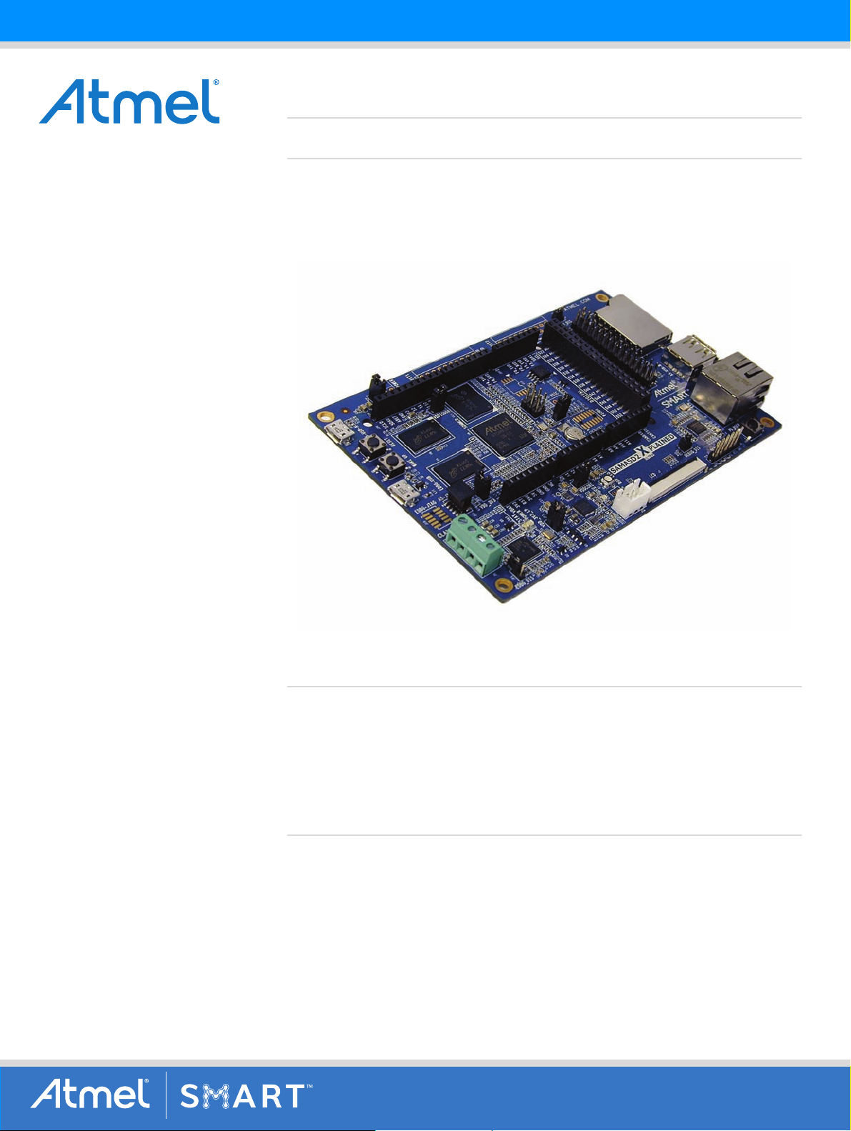
SAMA5D2 Xplained Ultra Evaluation Kit
USER GUIDE
Introduction
This user guide introduces the Atmel® SAMA5D2 Xplained Ultra evaluation kit
(SAMA5D2-XULT) and describes the development and debugging capabilities for
applications running on the Atmel | SMART SAMA5D2 ARM
®
Cortex®-A5-based
embedded microprocessor unit (eMPU).
Scope
This guide provides details on the SAMA5D2-XULT. It is made up of five main
sections:
Section 1. describes the evaluation kit content and its main features.
Section 2. provides instructions to power up the SAMA5D2-XULT board.
Section 3. provides information on obtaining sample code and technical
support.
Section 4. provides an overview of the SAMA5D2-XULT board.
Section 5. describes the SAMA5D2-XULT board components.
SMART
Atmel-44028B-ATARM-SAMA5D2-Xplained-Ultra-User Guide_02-Oct-15

Kit Contents
The SAMA5D2-XULT includes:
Board
One SAMA5D2-XULT board
Cables
One Micro-AB type USB cable
Welcome letter
2
SAMA5D2 Xplained Ultra [USER GUIDE]
Atmel-44028B-ATARM-SAMA5D2-Xplained-Ultra-User Guide_02-Oct-15

Table of Contents
Introduction. . . . . . . . . . . . . . . . . . . . . . . . . . . . . . . . . . . . . . . . . . . . . . . . . . . . . . . . . . . . . . . . . . . . . . . . . . . . 1
Scope . . . . . . . . . . . . . . . . . . . . . . . . . . . . . . . . . . . . . . . . . . . . . . . . . . . . . . . . . . . . . . . . . . . . . . . . . . . . . . . . . . 1
Kit Contents. . . . . . . . . . . . . . . . . . . . . . . . . . . . . . . . . . . . . . . . . . . . . . . . . . . . . . . . . . . . . . . . . . . . . . . . . . . . 2
Table of Contents . . . . . . . . . . . . . . . . . . . . . . . . . . . . . . . . . . . . . . . . . . . . . . . . . . . . . . . . . . . . . . . . . . . . . . 3
1. Evaluation Kit Specifications . . . . . . . . . . . . . . . . . . . . . . . . . . . . . . . . . . . . . . . . . . . . . . . . . . . . . 4
1.1 Electrostatic Warning . . . . . . . . . . . . . . . . . . . . . . . . . . . . . . . . . . . . . . . . . . . . . . . . . . . . . . . . . . . . . 4
1.2 Power Supply Warning . . . . . . . . . . . . . . . . . . . . . . . . . . . . . . . . . . . . . . . . . . . . . . . . . . . . . . . . . . . . 4
2. Power Source . . . . . . . . . . . . . . . . . . . . . . . . . . . . . . . . . . . . . . . . . . . . . . . . . . . . . . . . . . . . . . . . . . . . . 5
2.1 Power up the Board. . . . . . . . . . . . . . . . . . . . . . . . . . . . . . . . . . . . . . . . . . . . . . . . . . . . . . . . . . . . . . . 5
3. Sample Code and Technical Support . . . . . . . . . . . . . . . . . . . . . . . . . . . . . . . . . . . . . . . . . . . . . 6
4. Hardware Overview . . . . . . . . . . . . . . . . . . . . . . . . . . . . . . . . . . . . . . . . . . . . . . . . . . . . . . . . . . . . . . . 7
4.1 Introduction . . . . . . . . . . . . . . . . . . . . . . . . . . . . . . . . . . . . . . . . . . . . . . . . . . . . . . . . . . . . . . . . . . . . . 7
4.2 Equipment List. . . . . . . . . . . . . . . . . . . . . . . . . . . . . . . . . . . . . . . . . . . . . . . . . . . . . . . . . . . . . . . . . . . 7
4.3 Board Features . . . . . . . . . . . . . . . . . . . . . . . . . . . . . . . . . . . . . . . . . . . . . . . . . . . . . . . . . . . . . . . . . . 7
5. Board Components . . . . . . . . . . . . . . . . . . . . . . . . . . . . . . . . . . . . . . . . . . . . . . . . . . . . . . . . . . . . . . . 8
5.1 Board Overview. . . . . . . . . . . . . . . . . . . . . . . . . . . . . . . . . . . . . . . . . . . . . . . . . . . . . . . . . . . . . . . . . . 8
5.2 Connectors on board. . . . . . . . . . . . . . . . . . . . . . . . . . . . . . . . . . . . . . . . . . . . . . . . . . . . . . . . . . . . . . 9
5.3 Function Blocks. . . . . . . . . . . . . . . . . . . . . . . . . . . . . . . . . . . . . . . . . . . . . . . . . . . . . . . . . . . . . . . . . . 9
5.4 PIO Usage and Interface Connectors. . . . . . . . . . . . . . . . . . . . . . . . . . . . . . . . . . . . . . . . . . . . . . . . 22
5.5 PIO Usage on Expansion Connectors. . . . . . . . . . . . . . . . . . . . . . . . . . . . . . . . . . . . . . . . . . . . . . . . 44
5.6 SAMA5D2-XULT Board Schematics. . . . . . . . . . . . . . . . . . . . . . . . . . . . . . . . . . . . . . . . . . . . . . . . . 57
6. Revision History . . . . . . . . . . . . . . . . . . . . . . . . . . . . . . . . . . . . . . . . . . . . . . . . . . . . . . . . . . . . . . . . . 72
SAMA5D2 Xplained Ultra [USER GUIDE]
Atmel-44028B-ATARM-SAMA5D2-Xplained-Ultra-User Guide_02-Oct-15
3
1. Evaluation Kit Specifications
WARNING
Electrostatic
sensitive
device
WARNING
WARNING
Table 1-1. Evaluation Kit Specifications
Characteristic Specifications
Board SAMA5D2-XULT
Board supply voltage USB and/or Battery powered
Temperature
Relative Humidity 0 to 90% (non-condensing)
Dimensions: Main board 135 × 88 × 20 mm
RoHS status Compliant
Board Identification SAMA5D2 XPLAINED ULTRA
1.1 Electrostatic Warning
Operating 0°C to +70°C
Storage -40°C to +85°C
ESD-Sensitive Electronic Equipment!
The evaluation kit is shipped in a protect ive anti-static pa ckage. The board sys tem
must not be subject to high electrostatic potentials.
We recommend using a grounding strap or similar ESD protective device when
handling the board in hostile ESD environments (off ices with sy nthe tic car pet , for
example). Avoid touching the component pins or any other metallic element on
the board.
1.2 Power Supply Warning
Hardware Power Supply Limitation
Powering the board with voltages higher than 5 VCC (e.g., the 12 VCC power
adapters from other kits such as Arduino kits) may damage the board.
Hardware Power Budget
Using the USB as the main power source (max. 500 mA) is acce ptable only with the
use of the on-board peripherals and low-power LCD extension.
When external peripheral or add-on boards need to be powered, we recommend
the use of an external power adapter connected to the USB Micro-AB connectors
(can provide up to 1.2A on the 3.3V node).
4
SAMA5D2 Xplained Ultra [USER GUIDE]
Atmel-44028B-ATARM-SAMA5D2-Xplained-Ultra-User Guide_02-Oct-15
2. Power Source
WARNING
Several options are available to power up the SAMA5D2-XULT board:
USB-powered through the USB Micro-AB connector (J23 - defa ult configuration)
Powered through a rechargeable battery Li-polymer 3.7V connected to J3 or J4
Powered through the USB Micro-AB connector on the Atmel Embedded Debugger (EDBG) interface (J14)
2.1 Power up the Board
Unpack the board, taking care to avoid electrostatic discharge. Connect the USB Micro-AB cable to the connector
(J23). Then connect the other end of the cable to a free USB port of your PC.
Table 2-1. Electrical Characteristics
Electrical Parameter Value
Input voltage 5 VCC
Maximum Input voltage (limits) 6 VCC
Maximum DC 3.3V current available 1.2A
I/O voltage 3.3V only
Unlike Arduino Uno boards, the SAMA5D2-XULT board runs at 3.3V. The maximum
voltage that the I/O pins can tolerate is 3.3V. Providing higher voltages (e.g., 5V) to
an I/O pin could damage the board.
SAMA5D2 Xplained Ultra [USER GUIDE]
Atmel-44028B-ATARM-SAMA5D2-Xplained-Ultra-User Guide_02-Oct-15
5

3. Sample Code and Technical Support
WARNING
After boot up, you can run some sample code or your own application on the development kit. You can download
sample code and get technical support from www.atmel.com.
Linux software and demos can be found on http://www.at91.com/linux4sam/bin/view/Linux4SAM/.
Please make sure to load the latest software version before starting your
evaluation. For more information, please go to
http://www.at91.com/linux4sam/bin/view/Linux4SAM/.
SAMA5D2 Xplained Ultra [USER GUIDE]
Atmel-44028B-ATARM-SAMA5D2-Xplained-Ultra-User Guide_02-Oct-15
6
4. Hardware Overview
4.1 Introduction
The Atmel SAMA5D2XULT is a full-featured evaluation platform for the Atmel SAMA5D2 series ARM-based
embedded microprocessor units (eMPU). It allows users to extensively evaluate, prototype and create applicationspecific designs.
4.2 Equipment List
The SAMA5D2-XULT board is based on the integration of an ARM Cortex-A5-based microprocessor with external
memory, one Ethernet physical layer transceiver, one SD/MMC interface, one host USB port and one device USB
port, one 24-bit RGB LCD and debug interfaces.
Seven headers, compatible with Arduino R3 (Uno, Due) and two Xplained headers are available for various shield
connections.
4.3 Board Features
Table 4-1. Board Specifications
Characteristics Specifications
Dimensions (L x W x H) 135 x 88 x 20 mm
Processor SAMA5D27 (289-ball BGA package), 14x14 mm body, 0.8 mm ball pitch
MPU, EDBG: 12 MHz crystal
Oscillators
Main Memory
Accessory memories
SD/MMC One 4-bit SD card connector
USB
Display
Image Sensor One ISC interface and connector
Ethernet One Ethernet PHY (RMII 10/100 MHz)
Debug port
Expansion connector
Board supply voltage
Battery On-board PowerCap
RTC: 32.768 kHz
PHY: 25 MHz
2 x DDR3L SDRAM 2 Gbit - 16 Mbit x 16 x 8 banks (total 4 Gbit = 512 Mbyte)
1 x eMMC NAND Flash 4 Gbit
One Serial EEPROM SPI
One optional QSPI Serial Flash
One EEPROM with MAC Address and Serial Number
One USB Host with power switch
One Micro-AB USB device
One LCD interface connector, LCD TFT Controller with overlay, alpha-blending, rotation, scaling and color
space conversion
One JTAG interface connector
One EDBG interface with CDC
One serial debug console interface (3v3 level)
Arduino R3 compatible set of connectors
XPRO set of connectors
5V from USB
On-board power regulation by PMIC
External Battery powered capability
User interface
7
SAMA5D2 Xplained Ultra [USER GUIDE]
Atmel-44028B-ATARM-SAMA5D2-Xplained-Ultra-User Guide_02-Oct-15
Reset, Wake-up and free user push button
One tri-color user LED (red, green, blue)
5. Board Components
R18
R11
R24
C1
C3
TP3
C2
R17
R16
R15
R14
Q1
C8
R9
R8
Q2
C9
R10
R23
C5
C6
R5
R1
TP1 TP2
J1
R27
R22
R21
R7
R6
C7
C11
R12
R25
U1
C4
JP1
BP1
C12
L2
R35
R31
R32
R34
R33
R39
R36
R37
R38
J2
R28
J3
R26
R20
R19
L1
C13
L3
Q3
C10
R13
C14
R29
R2R3R4
L4
J5
C18
C16
R48
R45
R47
JP2
R40
R42
J4
R30
R41
D1
U2
C17
C20
TP5
Y1
D4
R46
D3
C15
R43
TP4
Q4
C21
J6
R64
U3
R61
R60
R49
C25
D2
R44
C19
C22
L6
L5
TP6
JP3
C24
R59
C35
C34
R70
R69
R68
R67
C36
C31
C28
C29
C30
C27
JP4
C37
TP7
C23
R63
C33
C26
Q5
Y2
R66
R65
J9
J8
C38
R58
R57
R56
R55
R54
R53
C39
R52
R51
R50
R71
R62
C32
R73
R72
J17
R81
R80
R79
R78
R77
R76
Y3
L10
J7
L7L8L9
R74
J11
C42
R123
R105
R100
C41
C40
R96
R95
R94
R93
R92
R91
R90
R89
R88
R87
R86
R85
R84
R83
R82
JP5
R75
J10
J13
J12
C43
R103
R122
R121
R120
R119
R118
R117
R116
R115
R114
R113
R112
R111
R110
R109
R108
R124
R104
R99
R130
C44
R129
C45
R131L12
L11
J18
R137
R136
R135
R134
R133
R132
JP6
C46
Y4
R138
C47
TP8
R102R101
79R89R
U5
J14
J19
R152
R146
C51
R143R142
R141R140
R139
C48
R128R127
R126R125
R107R106
U4
C50
C49
L13
U7
J15
R154
R151
R150
R149
R148
R147
R145
R144
U6
R153
U8
R158
R155
C52
J16
R163
R161
R159
R156
R162
R160
R157
BP2
U9
C53
U10
R169
R167
R165
R164
U11
R177
R175
R173
R171
R182
R181
C55
R180
C54
R179
R178
J22
R172
R170
R168
R166
JP7
L14
C56
J20
BP3
J21
R176
R174
J23
J24
JP8
C60
C59
R184
R183
C57
JP9
J26
J25
C58
42
3
42
3
4
1
3
4
2
3
2
D22
SCL1
F3_RXD
SDA1
F0_RXD
F3_TXD
F0_TXD
F4_RXD
F4_TXD
GND
AREF
SDA0
SCL0
A5-USB-A
D23
V5V5
8
10
9
12
11
13
BOOT_DIS
211920
17
18
XPRO EXT2
161415
1
0
324
567
XPRO EXT1
XPRO POWER
VDD_5V_IN
F1_TXD
F1_RXD
WWW.ATMEL.COM
D51
D49
D50
D48
PIOBU
A5-JTAGEDBG-JTAG
D47
D46
EDBG-USB
SDMMC1
ISC
D45
D43
D44
D42
DIGITAL
VDDBU
D41
D40
B
B
D39
D37
D38
D36
HSIC
A
WAKE UP
D35
D33
D34
D32
SDMMC0
D31
D30
RESET
D29
D27
D28
D26
VDDIODDR
D25
D24
D53
GND
GND
D52
A
A5-USB-B
R
CANTX1
CANRX1
VDD_3V3
CANRX0
CANTX0
VBAT
STAT
ETH
A11
A10
A9
A8
A7
A6
A5
A4
A3
A2
A1
A0
NC
GND
GND
5V
3V3
RST
3V3
CLASS D
TM
VDDCORE
POWER
3.3V LEVELS
RTS GND
RXD VCCTXD
CTS
EDBG_DIS
DEBUG
PB_USER
DEBUG_DIS
LCD
Pin1
VBAT
RGB LED
VDD_3V3_LP
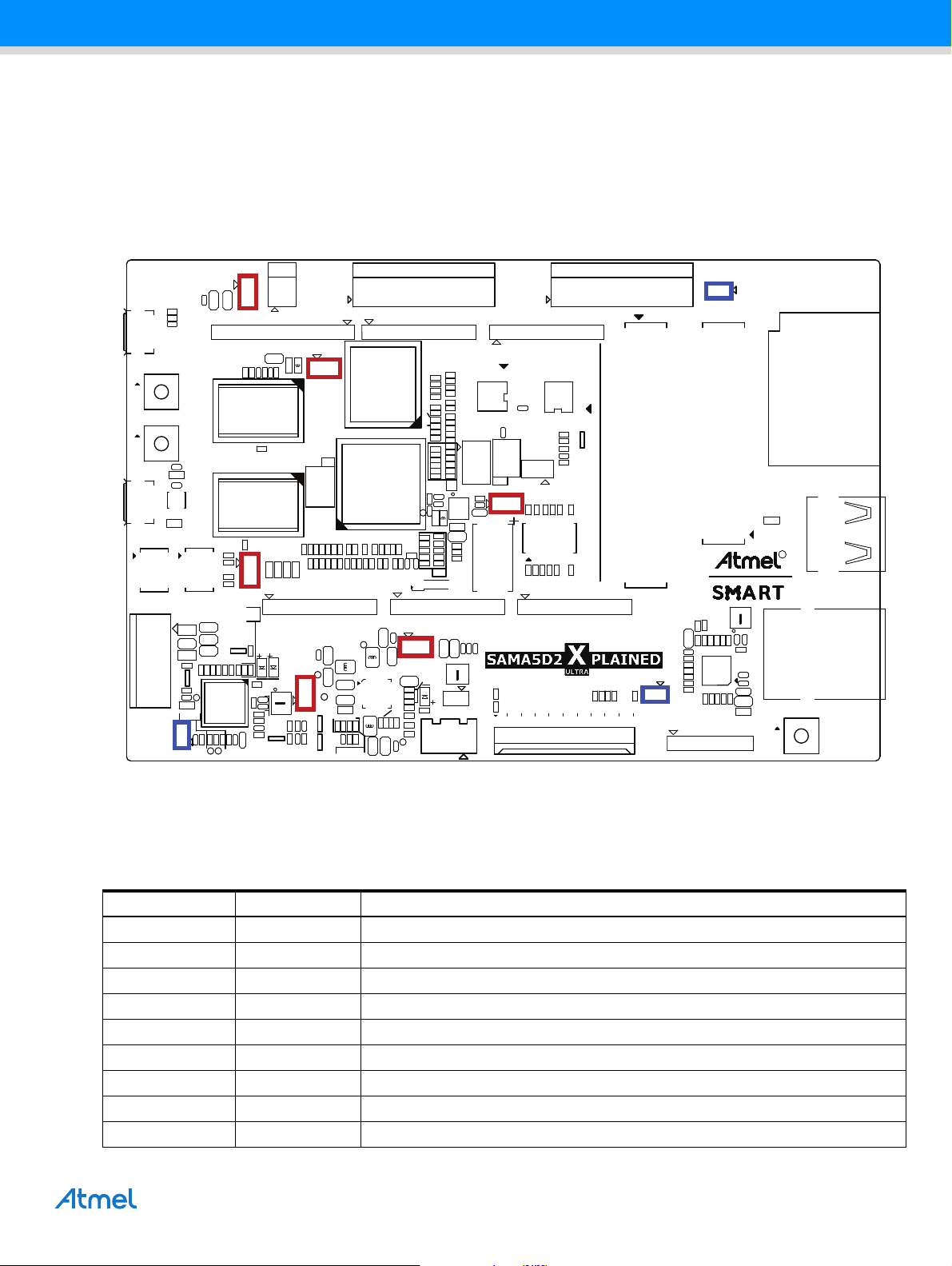
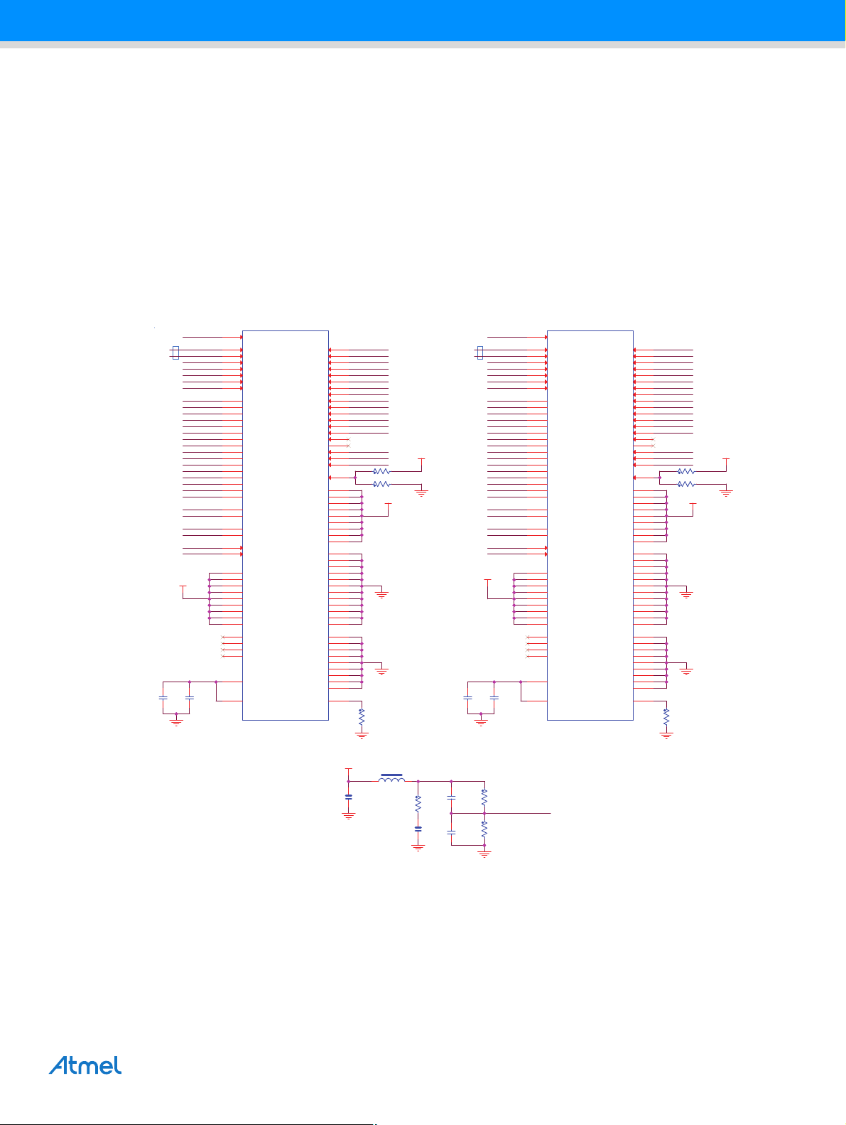
5.1 Board Overview
The fully-featured SAMA5D2-XULT board integrates multiple peripherals and in terface connectors as shown in
Figure 5-1.
Figure 5-1. SAMA5D2-XULT Board Overview
5.1.1 Default Jumper Settings
Figure 5-1 shows the default jumper settings. Blue jumpers are configuration items. Red jumpers are current
measurement points. Table 5-2 describes the functionality of the jumpers.
Table 5-1. SAMA5D2-XULT Jumper Settings
Jumper Default Function
JP1 OPEN Disable EDBG
JP2 OPEN Disable Debug
JP3 CLOSE VDD_3V3_LP current measurement
JP4 CLOSE VDDCORE current measurement
JP5 CLOSE VDDISC + VDDIOP0/1/2 current measurement
JP6 CLOSE VDDBU current measurement
JP7 CLOSE VDDIODDR_MPU current measurement
JP8 CLOSE VDD_5V_IN current measurement
JP9 OPEN Disable CS of SPI&QSPI&eMMC memories
8
SAMA5D2 Xplained Ultra [USER GUIDE]
Atmel-44028B-ATARM-SAMA5D2-Xplained-Ultra-User Guide_02-Oct-15
5.2 Connectors on board
Table 5-2 describes the interface connectors on the SAMA5D2-XULT.
Table 5-2. SAMA5D2-XULT Board Interface Connectors
Connector Interfaces to
J23 USB A Device. Supports USB device using a type Micro-AB connector
J13 USB Host B. Supports USB host using a type A connector
J1 Serial DBGU (3.3V level)
J11 JTAG, 10 pin IDC connector
J14 EDBG USB connector
J15 USB C (not populated)
J6 Ethernet
J2
J19 SDHCI SD/MMC connector
J3, J4 Battery connectors
J12 Tamper connector (not populated)
J7, J8, J9,
J16, J17,
J20, J21, J22
J24, J25, J26 Xplained Pro Expansion connectors
Expansion connector with all LCD controller signals for display module connection (QTouch
display with touchscreen and backlight)
Expansion connectors with Arduino R3 compatible PIO signals
®
, TFT LCD
J10 EDBG JTAG (not populated)
J18 ISC interface
J5 Class-D amplifier output
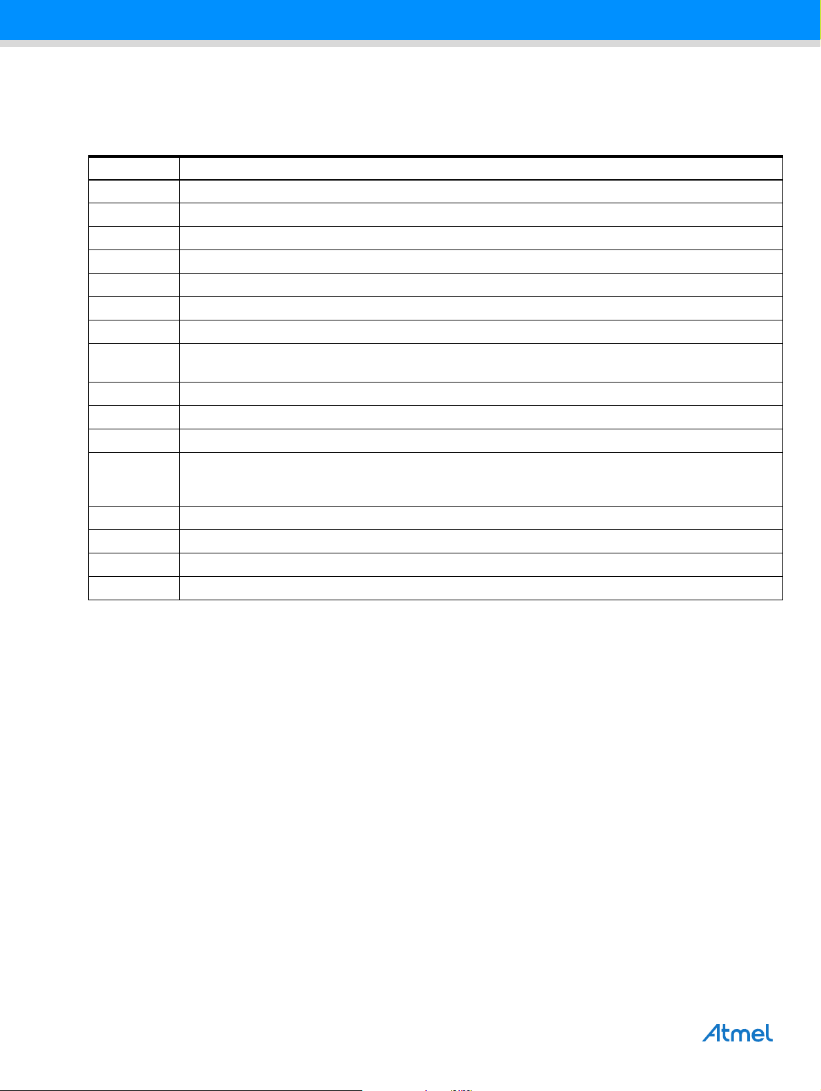
5.3 Function Blocks
5.3.1 Processor
The Atmel
ARM
5.3.2 Power Supply Topology and Power Distribution
5.3.2.1 Power Supplies
Detailed information on the device power supplies is provided in the tables “SAMA5D2 Power Supplies” and
“Power Supply Connections” in the SAMA5D2 Series datasheet.
®
®
| SMART SAMA5D2 Series is a high-performance, power-efficient embedded MPU based on the
Cortex®-A5 processor. Please refer to the SAMA5D2 Series datasheet for more information.
9
SAMA5D2 Xplained Ultra [USER GUIDE]
Atmel-44028B-ATARM-SAMA5D2-Xplained-Ultra-User Guide_02-Oct-15
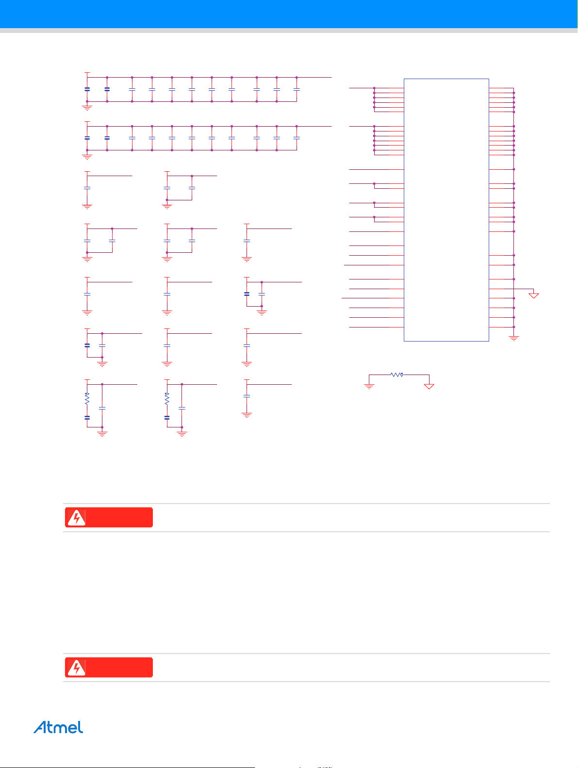
Figure 5-2. Processor Power Lines Supplies
(3V3)
(1V2)
(1V35)
(3V3)
(3V3) (3V3) (3V3)
(1V2) (2V5)
(3V3)
(3V3)
(3V3)
(3V3)
(3V3)
(3V3)
(3V3)
(3V3)
(3V3)
(1V35)
(1V2)
(1V2)
(1V2)
(1V2)
(2V5)
(3V3)
(1V2)
(1V2) (3V3)
(3V3)
(3V3)
(3V3 or 1V8)
(3V3 or 1V8)
VDDBU
VDDCORE
VDDPLLA
VDDIOP0
VDDIOP1
VDDIOP2
VDDHSIC
VDDUTMIC
VDDUTMII
VDDSDHC
VDDPLLA
VDDOSC
VDDISC
VDDFUSE
VDDAUDIOPLL
VDDBU
VDDIODDR
VDDANA
VDDANA
VDDIOP0 VDDIOP1 VDDIOP2
VDDHSIC VDDFUSE
VDDUTMII VDDSDHC
VDDOSC VDDISC
VDDUTMIC
VDDCORE
VDDIODDR
VDDAUDIOPLL
GNDUTMII
VDDBU
VDDCORE
VDDIODDR
VDDANA
VDDIOP0 VDDIOP1 VDDIOP2
VDDHSIC VDDFUSE
VDDUTMII VDDSDHC
VDDPLLA VDDOSC VDDISC
VDDUTMIC
GNDUTMII
VDDAUDIOPLL
C135
100nF
C31
100nF
C29
100nF
C128
100nF
C140
100nF
C132
100nF
C134
100nF
C43
4.7uF
C80
100nF
R269
1R 1%
C131
100nF
C102
100nF
C144
100nF
C27
10uF
C101
100nF
C136
100nF
C111
100nF
C118
100nF
C70
10uF
C97
1nF
C30
1nF
C108
100nF
C119
100nF
C142
4.7uF
C137
1nF
C28
10uF
C110
100nF
C138
100nF
R264 0R
C107
100nF
R131
1R 1%
C88
100nF
C71
10uF
C133
100nF
C104
100nF
C45
100nF
C120
100nF
C105
1nF
C125
100nF
C114
100nF
SAMA5D27-CN
U6G
GNDANA_2
K5
GNDBU
N6
GNDCORE_1
E7
GNDCORE_2
E9
GNDCORE_3
H4
GNDCORE_4
K12
GNDCORE_5
M5
GNDCORE_6
M9
GNDDDR_1
D14
GNDDDR_2
E11
GNDDDR_3
E12
GNDDDR_4
E14
GNDDDR_5
H14
GNDDDR_6
J14
GNDDDR_7
L14
GNDDPLL
T5
GNDAUDIOPLL
T4
GNDIOP0_1
F6
GNDIOP0_2
G7
GNDIOP1_1
M13
GNDIOP1_2
P14
GNDIOP2
F9
GNDISC
G4
GNDOSC
T6
GNDPLLA
U5
GNDSDMMC
R11
GNDUTMII
P9
GNDUTMIC
R7
VDDANA_2
L5
VDDBU
N7
VDDCORE_1
D7
VDDCORE_2
D9
VDDCORE_3
H3
VDDCORE_4
K13
VDDCORE_5
N5
VDDCORE_6
N9
VDDDDR_1
D11
VDDDDR_2
D12
VDDDDR_3
D15
VDDDDR_4
E15
VDDDDR_5
H15
VDDDDR_6
J15
VDDDDR_7
L15
VDDAUDIOPLL
T3
VDDFUSE
M12
VDDHSIC
R9
VDDIOP0_1
E6
VDDIOP0_2
F7
VDDIOP1_1
N13
VDDIOP1_2
R14
VDDIOP2
F10
VDDISC
F4
VDDOSC
T7
VDDPLLA
U4
VDDSDMMC
P11
VDDUTMII
P8
VDDUTMIC
P7
GNDANA_1
L3
VDDANA_1
K3
C122
1nF
C147
4.7uF
C103
100nF
C84
1nF
C143
100nF
C148
4.7uF
WARNING
WARNING
5.3.2.2 Power-up and Power-down Considerations
Power-up and power-down considerations are described in section “Power Considerations” of the SAMA5D2
Series datasheet.
5.3.2.3 ACT8945A Power Management IC
The ACT8945A is a complete, cost-effective and highly-efficient ActivePMU™ power management solution,
optimized to provide a single-chip power solution and voltage sequencing for Atmel
The power-up sequence provided in the SAMA5D2 Series datasheet must be
respected for reliable operation.
SAMA5D2/SAMA5D3/SAMA5D4 and SAM9 series MPUs. It also meets the contro l requirements of these de vices.
The ACT8945A features three step-down DC-DC converters and four low-noise, low-dropout linear regu lators
along with a complete battery charging solution featuring the advanced ActivePath™ system-power selection
function.
Refer to the ACT8945A datasheet at www.active-semi.com for more details.
SAMA5D2 Xplained Ultra [USER GUIDE]
Atmel-44028B-ATARM-SAMA5D2-Xplained-Ultra-User Guide_02-Oct-15
10
The three DC-DC converters utilize a high efficiency, fixed-frequency (2 MHz), current-mode PWM control
architecture that requires a minimum number of external components. Two DC-DC converters are capable of
supplying up to 1100 mA of output current, while t he third supports up to 1200 mA. All four low-dropout linear
regulators are high performance, low-noise regulators that supply up to 320 mA of output current.
Figure 5-3. Board Power Management
JP8
U12
D9
VDD_3V3
C10 100nF
(See note 1)
1
R610K
DNP(8.2K 1%)
R15
100K
3
VSYS_5V
2
8
3
2
Q7
DNP
(IRLML6402)
R710K
nPBSTAT
R26
R12
100K
IN1
VSNS
EN
IN26GND
TPS2113
32
C8
100nF
R13
49.9K 1%
1
Q3
BSS138
STAT
OUT
ILIM
C165
4.7uF
EDBG_USB_VBUS_5V[14]
USBA_VBUS_5V[10]
5V_EXT_INP[15]
DNP(11K 1%)
PMIC_CHGLEV_PA12[7]
PMIC_IRQ_PB13[7]
PMIC_LBO/EXP_PC8[8,15]
PMIC_TWD0_PD21[8]
PMIC_TWCK0_PD22[8]
SHDN[9]
1
Q2
BSS138
VDD_5V_IN
R11
(3.9K 1%)
R24
DNP
NRST[9,10,12,14,15]
R8
68K
3
2
R9 1K
R187 10K
R186 10K
(replaced with 0R-1206
- see User Guide)
R18
11K 1%
VSYS_5V
1
Q1
BSS138
Header 1X2
1
7
4
R185 390R 1%
5
VIN_5V
VBAT
R21 2.2M 1%
R22 1.5M 1%
R27
2.43K 1%
R16 100R 1%
R17 100R 1%
R20 100R 1%
VSYS_5V
C7
DNP(1nF)
R30 0R
R41 DNP(0R)
R14 49.9K 1%
TP11
TP14
SMD
SMD
3
BP2Tact Switch
2
WAKE UP RESET
1
2
C166
47nF
JPR8
Jumper
33
21
20
23
1
22
11
12
13
19
27
26
25
10
9
BP3Tact Switch
VDD_5V_IN
C59
10uF
U2 ACT8945AQJ405-T
CHGIN
ACIN
LBI
ISET
REFBP
CHGLEV
nRSTO
nIRQ
nPBSTAT
nLBO
SDA
SCL
VSEL
PWRHLD
nPBIN
R19
0R
C58
C60
100nF
10uF
GNDA3PWREN18GNDP1237GNDP314EXPAD
41
VSYS_5V VDDB_5V
R34510K
C180
10uF
31
VSYS1
32
VSYS2
39
VP1
35
VP2
16
VP3
6
INL
40
NC1
28
R44 100R 1%
nSTAT
29
BAT1
30
BAT2
24
TH
38
L5 2.2uH
SW1
2
OUT1
36
L6 2.2uH
SW2
34
OUT2
15
L1 2.2uH
SW3
17
OUT3
4
OUT4
5
OUT5
8
OUT6
7
OUT7
L27
0.47uH
VBAT
VDD_2V5
VDD_3V3
VDD_3V3
VDD_1V8
C169
4.7uF
U22
A3
B1
B2
B3
1
2
3
C17
4.7uF
VIN
SW1
SW2
EN
FAN48610
C163
10uF
D1 RED
J3
1X3Pin
C173
4.7uF
C20
10uF
C22
10uF
C3
10uF
VOUT1
VOUT2
PGND1
PGND2
AGND
C164
10uF
VBAT
C19
4.7uF
C13
4.7uF
A1
A2
C1
C2
C3
C176
10uF
VSYS_5V
C23
10uF
C37
10uF
C2
10uF
R327 0R
R330 0R
180ohm at 100MHz
VSYS_5V
1
2
C181
22uF
C167
100nF
J4
DNP(Header 1X2 2.00MM)
VDD_1V35
C24
100nF
VDD_1V2
C38
100nF
VDD_3V3
C1
100nF
VDDFUSE
VDD_3V3_LP
L3
1 2
VDD_3V3
RB160M-60TR
VDD_1V35
For DDR3 For MPU
VDD_LED
VDDSDHC1V8
D5
Header 1X2
JP7
1
R280 100R 1%
JPR7
Jumper
2
VDD_3V3_LP
VDDIODDR
VDD_3V3
JP3
Header 1X2
1
+
(Super)-Capacitor
energy storage
VDD_1V2
JP5
Header 1X2
JPR3
Jumper
2
C42
0.2F/3.3V
1
2
D6
BAT54C
1
2
R129 2R2
JPR5
Jumper
R293 2R2
R284 0R
R303 0R
R300 2R2
3
C44
DNP(1uF)
JP4
Header 1X2
2
1
180ohm at 100MHz
180ohm at 100MHz
180ohm at 100MHz
180ohm at 100MHz
180ohm at 100MHz
180ohm at 100MHz
180ohm at 100MHz
180ohm at 100MHz
C46
100nF
JPR4
Jumper
L12 10uH_150mA
L18
1 2
L16
1 2
L7
1 2
L8
1 2
L9
1 2
L10
1 2
L20 10uH_150mA
L19
1 2
L23
1 2
L22 10uH_150mA
JPR6
Jumper
Populate R if
no Super Cap
VDDCORE
VDDPLLA
VDDUTMIC
VDDHSIC
VDDIOP2
VDDIOP1
VDDIOP0
VDDISC
VDDOSC
VDDUTMII
VDDANA
VDDAUDIOPLL
Header 1X2
R139
DNP(2.2K)
JP6
VDDBU
1
2
Note: 1. Occasional board startup problems occurred when powered from a USB source having a weak VBUS level below 4.8V. To
avoid the voltage drop and consequential startup problems, production boards were assembled with a 0 Ω resistor in place
of the Schottky diode D9 shown here.
Supply Group Configuration
The ACT8945A provides:
All power supplies required by the SAMA5D2 device:
1.2V VDDCORE, VDDPLLA, VDDUTMIC, VDDHSIC
1.35V VDDIODDR
2.0V VDDBU
3.3V VDDIOP, VDDISC, VDDEDBG
2.5V VDDFUSE
3.3V VDDOSC, VDDUTMI, VDDANA, VDDAUDIOPLL
Power supplies to external chips on the main board:
1.8V VDDSDHC1V8
2.5V VDDLED
4.8V VSYS_5V
11
SAMA5D2 Xplained Ultra [USER GUIDE]
Atmel-44028B-ATARM-SAMA5D2-Xplained-Ultra-User Guide_02-Oct-15
5.3.2.4 Power Boost 5V
To generate a true 5V voltage from the PMIC output (4.8V typical), a FAN48610 low-power boost re gulator is
integrated into the design. This feeds the 5V USB host and the 5V LCD.
Figure 5-4. Power Boost 5V
5.3.2.5 Input Power Options
There are several power options for the SAMA5D 2- XUL T board .
The USB-powered operation is the default configuration. It comes from the USB device port connected to a PC or
a 5V DC supply. The USB supply is sufficient to power the board in most applications. It is important to note that
when the USB supply is used, the USB-B Host port has limited power. If USB Host port is required for the
application, it is recommended that an external DC supply be used.
Figure 5-5 provides the schematics of power options.
VSYS_5V VDDB_5V
A3
C180
10uF
R34510K
L27
0.47uH
B1
B2
B3
VIN
SW1
SW2
EN
U22
VOUT1
VOUT2
PGND1
PGND2
FAN48610
AGND
A1
A2
C1
C2
C3
C181
22uF
Figure 5-5. Input Powering Scheme
EDBG_USB_VBUS_5V[14]
USBA_VBUS_5V[10]
Note: USB-powered operation eliminates additional wires and batteries. It is the preferred mode of operation for
any project that requires only a 5V source at up to 500 mA.
5.3.2.6 Battery Supply Source
The ACT8945A features an advanced battery charger that incorporates the ActivePath architecture for system
power selection. This combination of circuits provides a complete, advanced battery-management system that
automatically selects the best available input supply, manages charge current to ensure system power availability,
and provides a complete, high accuracy (±0.5%), thermally regulated, full-featured single-cell linear Li+ charger .
The ActivePath circuitry monitors the state of the input supply, the battery, and the system, and automatically
reconfigures itself to optimize the power system. If a valid input supply is present, ActivePath powers the system
from the input while charging the battery in parallel. This allows the battery to charge as quickly as possible, while
supplying the system. If a valid input supply is not present, ActivePath powers the system from the battery. Finally,
if the input is present and the system current requirement exceeds the capability of the input supply, ActivePath
allows system power to be drawn from both the battery and the input supply.
R187 10K
R186 10K
8
IN1
3
VSNS
2
EN
IN26GND
U12
STAT
TPS2113
OUT
ILIM
1
7
4
R185 390R 1%
5
JP8
Header 1X2
1
2
JPR8
Jumper
VDD_5V_IN
C59
10uF
C60
10uF
C58
100nF
SAMA5D2 Xplained Ultra [USER GUIDE]
Atmel-44028B-ATARM-SAMA5D2-Xplained-Ultra-User Guide_02-Oct-15
12
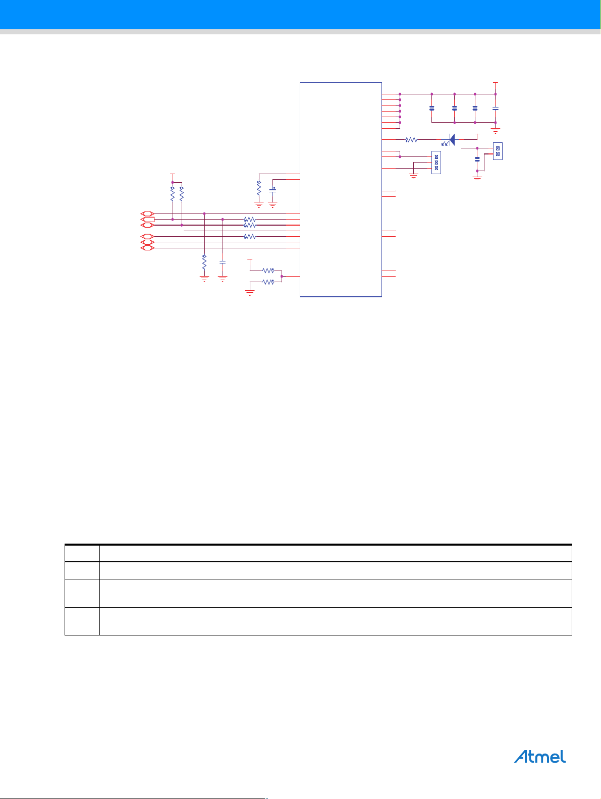
Figure 5-6. Battery Powering Scheme
nPBSTAT
VBAT
VBAT
VSYS_5V
VSYS_5V
VSYS_5V
VDD_3V3
PMIC_CHGLEV_PA12[7]
PMIC_IRQ_PB13[7]
PMIC_TWD0_PD21[8]
PMIC_TWCK0_PD22[8]
NRST[9,10,12,14,15]
PMIC_LBO/EXP_PC8[8,15]
C19
4.7uF
R17 100R 1%
R30 0R
J3
1X3Pin
1
2
3
R26
DNP(8.2K 1%)
R16 100R 1%
R710K
R27
2.43K 1%
R44 100R 1%
C7
DNP(1nF)
R610K
R20 100R 1%
C166
47nF
J4
DNP(Header 1X2 2.00MM)
1
2
C164
10uF
C163
10uF
C167
100nF
D1 RED
R41 DNP(0R)
C176
10uF
U2 ACT8945AQJ405-T
CHGIN
33
ACIN
21
LBI
20
ISET
23
REFBP
1
CHGLEV
22
nRSTO
11
nIRQ
12
nPBSTAT
13
nLBO
19
SDA
27
SCL
26
VSEL
25
VSYS1
31
VSYS2
32
VP1
39
VP2
35
VP3
16
INL
6
NC1
40
nSTAT
28
BAT1
29
BAT2
30
TH
24
SW1
38
OUT1
2
SW2
36
OUT2
34
SW3
15
OUT3
17
Charger Input Interrupts
In order to ease input supply detection and eliminate the size and cost of external detection circuitry, the charger
has the ability to generate interrupts based upon the status of the input supply. This function is capable of
generating an interrupt when the input is connected, disconnected, or both, whe n the charger state machine
transitions.
Charge Status Indicator
The charger provides a charge-status indicator output, nSTAT. nSTAT is an open-drain output which sinks current
when the charger is in an active-charging state, and is high-Z otherwise. nSTAT features an internal 8 mA current
limit, and is capable of directly driving a LED (D1).
Precision Voltage Detector
The LBI input connects to one input of a precision voltage comparator, which can be used to monitor a system
voltage such as the battery voltage. An external resistive-divider network can be used to set voltage monitoring
thresholds. The output of the comparator is present at the nLBO open-drain output and connected to the led red
D1.
Table 5-3. PIOs Used to Control the Battery Charger
PIO Function
PA12 CHGLEV: Charge Current Selection Input
PB13
PC8
13
SAMA5D2 Xplained Ultra [USER GUIDE]
Atmel-44028B-ATARM-SAMA5D2-Xplained-Ultra-User Guide_02-Oct-15
nIRQ: Open-Drain Interrupt Output. nIRQ is asserted any time an unmasked fault condition exists or a charger
interrupt occurs.
nLBO: Low Battery Indicator Output. nLBO is asserted low whenever the voltage at LBI is lower than1.2V; it is highZ otherwise.
Figure 5-7. Battery Connector J3 and Optional J4
R18
R11
R24
C1
C3
TP3
C2
R17
R16
R15
R14
Q1
C8
R9
R8
Q2
C9
R10
R23
C5
C6
R5
R1
TP1 TP2
J1
R27
R22
R21
R7
R6
C7
C11
R12
R25
U1
C4
JP1
BP1
C12
L2
R35
R31
R32
R34
R33
R39
R36
R37
R38
J2
R28
J3
R26
R20
R19
L1
C13
L3
Q3
C10
R13
C14
R29
R2R3R4
L4
J5
C18
C16
R48
R45
R47
JP2
R40
R42
J4
R30
R41
D1
U2
C17
C20
TP5
Y1
D4
R46
D3
C15
R43
TP4
Q4
C21
J6
R64
U3
R61
R60
R49
C25
D2
R44
C19
C22
L6
L5
TP6
JP3
C24
R59
C35
C34
R70
R69
R68
R67
C36
C31
C28
C29
C30
C27
JP4
C37
TP7
C23
R63
C33
C26
Q5
Y2
R66
R65
J9
J8
C38
R58
R57
R56
R55
R54
R53
C39
R52
R51
R50
R71
R62
C32
R73
R72
J17
R81
R80
R79
R78
R77
R76
Y3
L10
J7
L7L8L9
R74
J11
C42
R123
R105
R100
C41
C40
R96
R95
R94
R93
R92
R91
R90
R89
R88
R87
R86
R85
R84
R83
R82
JP5
R75
J10
J13
J12
C43
R103
R122
R121
R120
R119
R118
R117
R116
R115
R114
R113
R112
R111
R110
R109
R108
R124
R104
R99
R130
C44
R129
C45
R131L12
L11
J18
R137
R136
R135
R134
R133
R132
JP6
C46
Y4
R138
C47
TP8
R102R101
79R89R
U5
J14
J19
R152
R146
C51
R143R142
R141R140
R139
C48
R128R127
R126R125
R107R106
U4
C50
C49
L13
U7
J15
R154
R151
R150
R149
R148
R147
R145
R144
U6
R153
U8
R158
R155
C52
J16
R163
R161
R159
R156
R162
R160
R157
BP2
U9
C53
U10
R169
R167
R165
R164
U11
R177
R175
R173
R171
R182
R181
C55
R180
C54
R179
R178
J22
R172
R170
R168
R166
JP7
L14
C56
J20
BP3
J21
R176
R174
J23
J24
JP8
C60
C59
R184
R183
C57
JP9
J26
J25
C58
42
3
42
3
4
1
3
4
2
3
2
D22
SCL1
F3_RXD
SDA1
F0_RXD
F3_TXD
F0_TXD
F4_RXD
F4_TXD
GND
AREF
SDA0
SCL0
A5-USB-A
D23
V5V5
8
10912
11
13
BOOT_DIS
211920
17
18
XPRO EXT2
161415
1
0
32456
7
XPRO EXT1
XPRO POWER
VDD_5V_IN
F1_TXD
F1_RXD
WWW.ATMEL.COM
D51
D49
D50
D48
PIOBU
A5-JTAGEDBG-JTAG
D47
D46
EDBG-USB
SDMMC1
ISC
D45
D43
D44
D42
DIGITAL
VDDBU
D41
D40
B
B
D39
D37
D38
D36
HSIC
A
WAKE UP
D35
D33
D34
D32
SDMMC0
D31
D30
RESET
D29
D27
D28
D26
VDDIODDR
D25
D24
D53
GND
GND
D52
A
A5-USB-B
R
CANTX1
CANRX1
VDD_3V3
CANRX0
CANTX0
VBAT
STAT
ETH
A11
A10
A9
A8
A7
A6
A5
A4
A3
A2
A1
A0
NC
GND
GND
5V
3V3
RST
3V3
CLASS D
TM
VDDCORE
POWER
3.3V LEVELS
RTS GND
RXD VCCTXD
CTS
EDBG_DIS
DEBUG
PB_USER
DEBUG_DIS
LCD
Pin1
VBAT
RGB LED
VDD_3V3_LP
Populate R if
no Super Cap
(Super)-Capacitor
energy storage
VDDBU
VDD_3V3
D6
BAT54C
3
1
2
C46
100nF
C44
DNP(1uF)
+
C42
0.2F/3.3V
R139
DNP(2.2K)
JPR6
Jumper
D5
RB160M-60TR
JP6
Header 1X2
1
2
R280 100R 1%
Table 5-4. Battery J3 Signal Descriptions
Pin Mnemonic Signal Description
1 VBAT Battery I/O (exploitation and charging). Connect this pin directly to the battery anode (+ terminal)
2 GND Common ground
3TH
5.3.2.7 Backup Power Supply
The SAMA5D2-XULT board requires a power source in order to permanently power the backup part of the
SAMA5D2 device (refer to SAMA5D2 Series datasheet). A super capacitor sustains such permanent power to
VDDBU when all system power sources are off.
Figure 5-8. VDDBU Powering Scheme Option
5.3.2.8 Power Supply Control
In the ACT8945A, three DC-DC converters (1.8V, 1.2V, 3.3V) and two LDO outputs are available.
All ACT8945A outputs can be controlled by the TWI interface through software.
Temperature Sensing Input. Conne ct to battery thermistor. TH is pulled up with a 102 μA (typical)
current internally.
SAMA5D2 Xplained Ultra [USER GUIDE]
Atmel-44028B-ATARM-SAMA5D2-Xplained-Ultra-User Guide_02-Oct-15
14
The three DC-DC outputs can be enabled or disabled by the SAMA5D2 SHDN output:
WAKE UP RESET
VSYS_5V
VSYS_5V
VSYS_5V
SHDN[9]
R30 0R
R14 49.9K 1%
Q2
BSS138
1
3
2
R12
100K
C8
100nF
R9 1K C10 100nF
TP11
SMD
BP3Tact Switch
R19
0R
R8
68K
R13
49.9K 1%
R20 100R 1%
Q1
BSS138
1
3
2
BP2Tact Switch
Q3
BSS138
1
3
2
TP14
SMD
R41 DNP(0R)
R15
100K
nPBSTAT
nLBO
19
SDA
27
SCL
26
VSEL
25
PWRHLD
10
GNDA
3
PWREN
18
GNDP1237GNDP314EXPAD
41
SW2
OUT2
34
SW3
15
OUT3
17
OUT4
4
OUT5
5
OUT6
8
OUT7
7
nPBIN
9
SHDN = 0: The DC-DC output is disabled.
SHDN = 1: The DC-DC output is enabled.
Two push buttons are also available:
Wakeup push button: When pressed, the ACT8945A power outputs are restarted if the ACT8945A is in
shutdown mode.
Reset push button: When pressed, the ACT8945A transfers the reset signal to the MPU.
5.3.3 Reset Circuitry
The reset sources for SAMA5D2-XULT bo ar d are:
Power-on reset from the power management unit (PMIC)
Push button reset BP3
External reset from Arduino connectors
JTAG or EDBG reset from an in-circuit emulator
Figure 5-9. Reset/Wakeup and Shutdown Control
5.3.4 Clock Circuitry
The SAMA5D2-XULT board includes four clock sources:
Two clocks are alternatives for the SAMA5D2 processor (12 MHz, 32 kHz)
One crystal oscillator used for the Ethernet RMII chip (25 MHz)
One crystal oscillator used for the EDBG (12 MHz)
Figure 5-10. Clock Circuitry
15
SAMA5D2 Xplained Ultra [USER GUIDE]
Atmel-44028B-ATARM-SAMA5D2-Xplained-Ultra-User Guide_02-Oct-15
C47
27pF
R146 DNP(1M)
Y4
1
2
4
3
12MHz CL=15pF
XIN
XOUT
C45
27pF
C41
22pF
R109
DNP(1M)
32.768KHz CL=12.5pF
Y3
1
23
4
XOUT32
XIN32
C40
22pF
C34 22pF
23
C35
25MHz CL=20pF
22pF
ETH_XI
1
Y2
4
R68
DNP(1M)
ETH_XO
5.3.5 Memory
5.3.5.1 Memory Organization
The SAMA5D2 features a DDR/SDR memory interface and an External Bus Interface (EBI) to permit interfacing to
a wide range of external memories and to almost any kind of parallel peripheral.
This section describes the memory devices that equip the SAMA5D2-XULT board.
5.3.5.2 DDR3/SDRAM
Two DDR3L/SDRAM (MT41H128M16JT-125-K - 2 Gbit = 16 Mbit x 16 x 8 banks) are used as main system
memory and totalling 4 Gbit of SDRAM on the board. The memory bus is 32 bits wide and operates with a
frequency of up to 166 MHz.
Figure 5-11. DDR3L
DDR_RESETN DDR_RESETN
DDR_CLK+
DDR_CLKDDR_CKE
DDR_CS
DDR_RAS
DDR_CAS
DDR_WE
DDR_D0
DDR_D1
DDR_D2
DDR_D3
DDR_D4
DDR_D5
DDR_D6
DDR_D7
DDR_D8
DDR_D9
DDR_D10
DDR_D11
DDR_D12
DDR_D13
DDR_D14
DDR_D15
DDR_DQS1+
DDR_DQS1-
DDR_DQS0+
DDR_DQS0-
DDR_DQM1
DDR_DQM0
VDD_1V35
DDR_VREF DDR_VREF
C72
C91
100nF
100nF
U8
T2
RESET#
J7
CK
K7
CK#
K9
CKE
L2
CS#
J3
RAS#
K3
CAS#
L3
WE#
E3
DQ0
F7
DQ1
F2
DQ2
F8
DQ3
H3
DQ4
H8
DQ5
G2
DQ6
H7
DQ7
D7
DQ8
C3
DQ9
C8
DQ10
C2
DQ11
A7
DQ12
A2
DQ13
B8
DQ14
A3
DQ15
C7
UDQS
B7
UDQS#
F3
LDQS
G3
LDQS#
D3
UDM
E7
LDM
A1
VDDQ1
A8
VDDQ2
C1
VDDQ3
C9
VDDQ4
D2
VDDQ5
E9
VDDQ6
F1
VDDQ7
H2
VDDQ8
H9
VDDQ9
J1
NC1
J9
NC2
L1
NC3
L9
NC4
M8
VREFCA
H1
VREFDQ
A10/AP
A12/BC#
ODT
VDD1
VDD2
VDD3
VDD4
VDD5
VDD6
VDD7
VDD8
VDD9
VSS1
VSS2
VSS3
VSS4
VSS5
VSS6
VSS7
VSS8
VSS9
VSS10
VSS11
VSS12
VSSQ1
VSSQ2
VSSQ3
VSSQ4
VSSQ5
VSSQ6
VSSQ7
VSSQ8
VSSQ9
MT41K128M16JT-125:K
U4
T2
DDR_A0
N3
A0
DDR_A1
P7
A1
DDR_A2
P3
A2
DDR_A3
N2
A3
DDR_A4
P8
A4
DDR_A5
P2
A5
DDR_A6
R8
A6
DDR_A7
R2
A7
DDR_A8
T8
A8
DDR_A9
R3
A9
DDR_A10
L7
DDR_A11
R7
A11
DDR_A12
N7
DDR_A13
T3
A13
T7
A14
M7
A15
DDR_BA0
M2
BA0
BA1
BA2
DDR_BA1
N8
DDR_BA2
M3
R179 DNP(1K)
K1
R178 0R R258 0R
B2
G7
R9
K2
K8
N1
N9
R1
D9
A9
B3
E1
G8
J2
J8
M1
M9
P1
P9
T1
T9
B1
B9
D1
D8
E2
E8
F9
G1
G9
L8
ZQ
VDD_1V35
VDD_1V35
R238
240R 1%
VDD_1V35
C145
100nF
DDR_CLK+
DDR_CLKDDR_CKE
DDR_CS
DDR_RAS
DDR_CAS
DDR_WE
DDR_D16
DDR_D17
DDR_D18
DDR_D19
DDR_D20
DDR_D21
DDR_D22
DDR_D23
DDR_D24
DDR_D25
DDR_D26
DDR_D27
DDR_D28
DDR_D29
DDR_D30
DDR_D31
DDR_DQS3+
DDR_DQS3-
DDR_DQS2+
DDR_DQS2-
DDR_DQM3
DDR_DQM2
C121
100nF
RESET#
J7
CK
K7
CK#
K9
CKE
L2
CS#
J3
RAS#
K3
CAS#
L3
WE#
E3
DQ0
F7
DQ1
F2
DQ2
F8
DQ3
H3
DQ4
H8
DQ5
G2
DQ6
H7
DQ7
D7
DQ8
C3
DQ9
C8
DQ10
C2
DQ11
A7
DQ12
A2
DQ13
B8
DQ14
A3
DQ15
C7
UDQS
B7
UDQS#
F3
LDQS
G3
LDQS#
D3
UDM
E7
LDM
A1
VDDQ1
A8
VDDQ2
C1
VDDQ3
C9
VDDQ4
D2
VDDQ5
E9
VDDQ6
F1
VDDQ7
H2
VDDQ8
H9
VDDQ9
J1
NC1
J9
NC2
L1
NC3
L9
NC4
M8
VREFCA
H1
VREFDQ
A10/AP
A12/BC#
VDD1
VDD2
VDD3
VDD4
VDD5
VDD6
VDD7
VDD8
VDD9
VSS1
VSS2
VSS3
VSS4
VSS5
VSS6
VSS7
VSS8
VSS9
VSS10
VSS11
VSS12
VSSQ1
VSSQ2
VSSQ3
VSSQ4
VSSQ5
VSSQ6
VSSQ7
VSSQ8
VSSQ9
MT41K128M16JT-125:K
ODT
DDR_A0
N3
A0
DDR_A1
P7
A1
DDR_A2
P3
A2
DDR_A3
N2
A3
DDR_A4
P8
A4
DDR_A5
P2
A5
DDR_A6
R8
A6
DDR_A7
R2
A7
DDR_A8
T8
A8
DDR_A9
R3
A9
DDR_A10
L7
DDR_A11
R7
A11
DDR_A12
N7
DDR_A13
T3
A13
T7
A14
M7
A15
DDR_BA0
M2
BA0
DDR_BA1
N8
BA1
DDR_BA2
M3
BA2
ZQ
K1
B2
G7
R9
K2
K8
N1
N9
R1
D9
A9
B3
E1
G8
J2
J8
M1
M9
P1
P9
T1
T9
B1
B9
D1
D8
E2
E8
F9
G1
G9
L8
R254 DNP(1K)
VDD_1V35
VDD_1V35
R124
240R 1%
VDDIODDR
C83
4.7uF
L14 10uH_150mA
R182
1R 1%
C56
4.7uF
C55
R181
100nF
6.8K 1%
DDR_VREF
R180
C54
6.8K 1%
100nF
SAMA5D2 Xplained Ultra [USER GUIDE]
Atmel-44028B-ATARM-SAMA5D2-Xplained-Ultra-User Guide_02-Oct-15
16
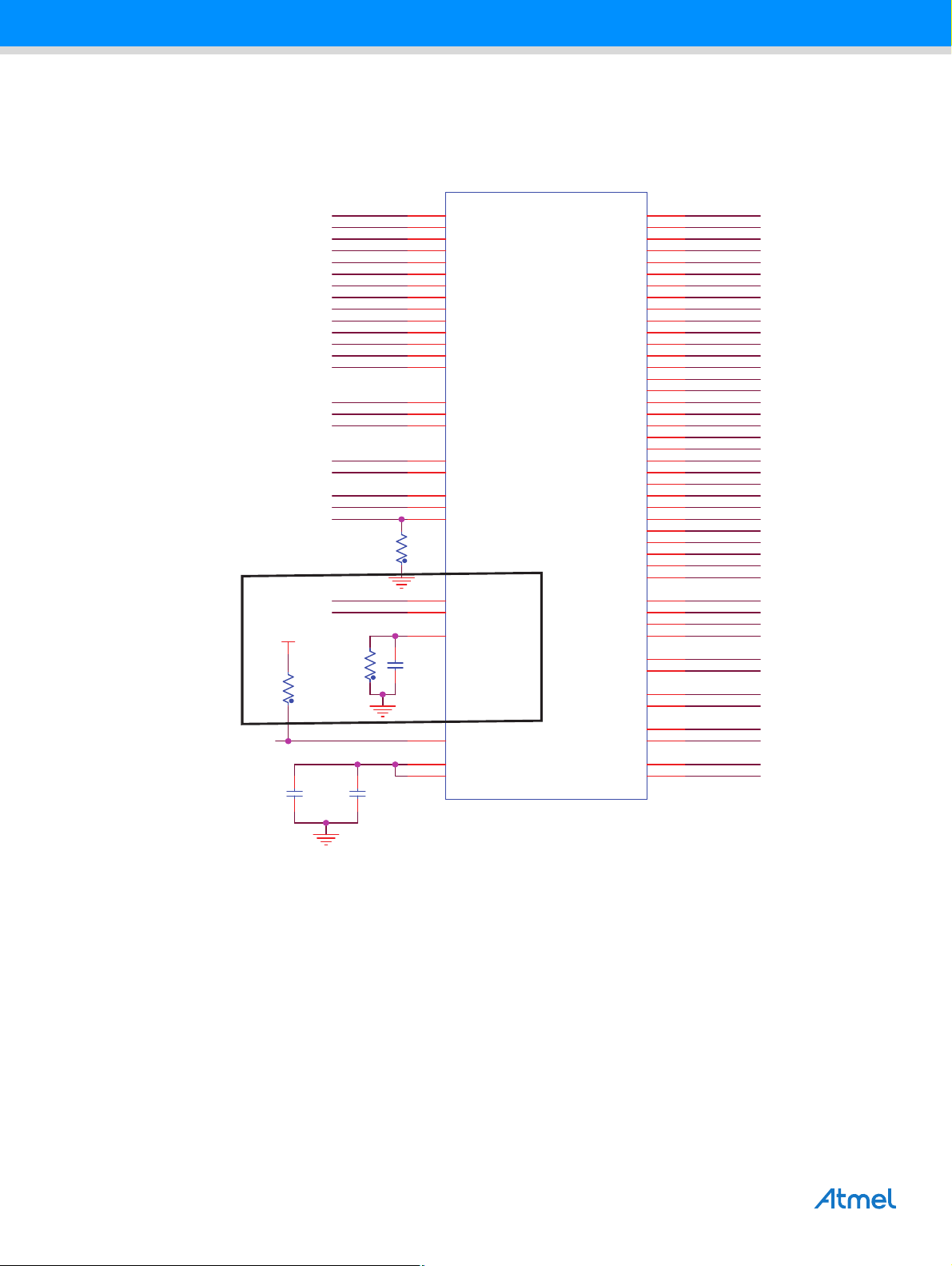
5.3.5.3 DDR_CAL Analog Input
One specific analog input, DDR_CAL, is used to calibrate all DDR I/Os.
Figure 5-12. DDR Signals and CAL Analog Input
VDD_1V35
DDR_RAS
DDR_CAS
DDR_CLK+
DDR_CLKDDR_CKE
DDR_CS
DDR_WE
23.2K 1%
R250
R242
100K
DDR_RESETN
DDR_VREF
C100
100nF
DDR_A0
DDR_A1
DDR_A2
DDR_A3
DDR_A4
DDR_A5
DDR_A6
DDR_A7
DDR_A8
DDR_A9
DDR_A10
DDR_A11
DDR_A12
DDR_A13
DDR_BA0
DDR_BA1
DDR_BA2
R243
100K
C99
100nF
F12
C17
B17
B16
C16
G14
F14
F11
C14
D13
C15
A16
A17
G11
H12
H13
F17
F13
G12
E17
D17
F16
G13
F15
E13
22pF
C106
E16
H16
D16
U6E
DDR_A0
DDR_A1
DDR_A2
DDR_A3
DDR_A4
DDR_A5
DDR_A6
DDR_A7
DDR_A8
DDR_A9
DDR_A10
DDR_A11
DDR_A12
DDR_A13
DDR_BA0
DDR_BA1
DDR_BA2
DDR_RAS
DDR_CAS
DDR_CLK
DDR_CLKN
DDR_CKE
DDR_CS
DDR_WE
DDR_CAL
DDR_RESETN
DDR_VREFB0
DDR_VREFCM
SAMA5D27-CN
DDR_D0
DDR_D1
DDR_D2
DDR_D3
DDR_D4
DDR_D5
DDR_D6
DDR_D7
DDR_D8
DDR_D9
DDR_D10
DDR_D11
DDR_D12
DDR_D13
DDR_D14
DDR_D15
DDR_D16
DDR_D17
DDR_D18
DDR_D19
DDR_D20
DDR_D21
DDR_D22
DDR_D23
DDR_D24
DDR_D25
DDR_D26
DDR_D27
DDR_D28
DDR_D29
DDR_D30
DDR_D31
DDR_DQM0
DDR_DQM1
DDR_DQM2
DDR_DQM3
DDR_DQS0
DDR_DQSN0
DDR_DQS1
DDR_DQSN1
DDR_DQS2
DDR_DQSN2
DDR_DQS3
DDR_DQSN3
B12
A12
C12
A13
A14
C13
A15
B15
G17
G16
H17
K17
K16
J13
K14
K15
B8
B9
C9
A9
A10
D10
B11
A11
J12
H10
J11
K11
L13
L11
L12
M17
C11
G15
C8
H11
B13
B14
J17
J16
C10
B10
L17
L16
DDR_D0
DDR_D1
DDR_D2
DDR_D3
DDR_D4
DDR_D5
DDR_D6
DDR_D7
DDR_D8
DDR_D9
DDR_D10
DDR_D11
DDR_D12
DDR_D13
DDR_D14
DDR_D15
DDR_D16
DDR_D17
DDR_D18
DDR_D19
DDR_D20
DDR_D21
DDR_D22
DDR_D23
DDR_D24
DDR_D25
DDR_D26
DDR_D27
DDR_D28
DDR_D29
DDR_D30
DDR_D31
DDR_DQM0
DDR_DQM1
DDR_DQM2
DDR_DQM3
DDR_DQS0+
DDR_DQS0-
DDR_DQS1+
DDR_DQS1-
DDR_DQS2+
DDR_DQS2-
DDR_DQS3+
DDR_DQS3-
17
SAMA5D2 Xplained Ultra [USER GUIDE]
Atmel-44028B-ATARM-SAMA5D2-Xplained-Ultra-User Guide_02-Oct-15
5.3.5.4 eMMC
The Secure Digital Multimedia Card (SDMMC) Controller supports the Embedded MultiMedia Card (e.MMC)
Specification V4.41, the SD Memory Card Specification V3.0, and the SDIO V3.0 specification. It is compliant with
the SD Host Controller Standard V3.0 specification
One MTFC4GLDEA 4 GB eMMC is connected to the processor through the SDMMC0 port.
Table 5-5. SDMMC Reference Documents
Name Link
SD Host Controller Simplified Specification V3.00 www.sdcard.org
SDIO Simplified Specification V3.00 www.sdcard.org
Physical Layer Simplified Specification V3.01 www.sdcard.org
Embedded MultiMedia Card (e.MMC) Electrical Standard 4.51 www.jedec.org
Figure 5-13. eMMC
VDDSDHC
VDD_3V3
R23747K
R14247K
R14447K
R14747K
SDHC0_DAT0_PA2[7]
SDHC0_DAT1_PA3[7]
SDHC0_DAT2_PA4[7]
SDHC0_DAT3_PA5[7]
SDHC0_DAT4_PA6[7]
SDHC0_DAT5_PA7[7]
SDHC0_DAT6_PA8[7]
SDHC0_DAT7_PA9[7]
SDHC0_CMD_PA1[7]
SDHC0_CK_PA0[7]
SDHC0_RSTN_PA10[7]
VDDSDHC
VDD_3V3
SDHC0_VDDSEL_PA11[7]
R140 39R
R235
47K pull down on SDHC0_CMD_PA1 close to MPU.
DNP(47K)
39R on SDHC0_CK_PA0 close to MPU.
R225
10K
C81
100nF
VDD_3V3
(3V3)
C73
2.2uF
R210 DNP(0R)
R212 DNP(0R)
VDD_3V3
2
VDD
6
S2
4
1
D
S1
IN
GND
3
U13
ADG849
(3V3 or 1V8)
C61
2.2uF
VDDSDHC1V8 VDDSDHC
R23447K
R15147K
C69
100nF
C86
100nF
5
R211 0R
IN=0: S1 Closed
IN=1: S2 Closed
R23347K
R255DNP(47K)
R23247K
R14947K
R23647K
A3
DAT0
A4
DAT1
A5
DAT2
B2
DAT3
B3
DAT4
B4
DAT5
B5
DAT6
B6
DAT7
M5
CMD
M6
CLK
K5
RST
K6
NC123
N6
NC122
E5
NC121
N9
NC120
N8
NC119
N7
NC118
J12
NC117
P14
NC116
N3
NC115
P10
NC114
N1
NC113
M14
NC112
M13
NC111
M12
NC110
M11
NC109
M10
NC108
M9
NC107
M8
NC106
M7
NC105
P11
NC104
P12
NC103
P13
NC102
M3
NC101
M2
NC100
M1
NC99
L14
NC98
L13
NC97
L12
NC96
A10
NC95
A11
NC94
A12
NC93
A13
NC92
A14
NC91
B1
NC90
B7
NC89
G1
NC88
L3
NC87
L2
NC86
L1
NC85
K14
NC84
K13
NC83
K12
NC82
VDDSDHC
(3V3 or 1V8)
C85
C79
1uF
E7
N4
C6
P5
F5
E6
K9
P3
J10
VCC1
VCC0
NC81
NC79
NC80
G2
G3
K10
VCC2
VCC3
VCCQ1
VCCQ3
VCCQ2
Impedance match of
CLK/CMD/DAT[7:0] 50R
NC78
NC74
NC77
NC75
NC73
NC76
K7
K3
B8
N11
N10
G10
M4
VCCQ5
VCCQ4
NC70
NC69
NC71
NC67
NC72
NC68
K2
K1
J14
J13
N13
N12
U11 MTFC4GLDEA-0M WT
N2
N14
P6
VSSQ1
VSSQ2
NC66
NC65
P1
P4
P2
C4
VSSQ3
VSSQ4
NC63
NC64
P7
K8
N5
G5
H10
C2
E1
NC1
E2
NC2
VDDI
VSS2
VSS4
VSS5
VSS1
VSS3
NC61
NC58
NC60
NC62
NC59
J2
J5
J3
P8
P9
E3
NC3
A2
NC4
A6
NC5
A7
NC6
A8
NC7
E8
NC8
E9
NC9
E10
NC10
A1
NC11
E12
NC12
E13
NC13
E14
NC14
F1
NC15
F2
NC16
F3
NC17
A9
NC18
B14
NC19
C14
NC20
C13
NC21
C12
NC22
C11
NC23
F10
NC24
C10
NC25
F12
NC26
F13
NC27
F14
NC28
C9
NC29
C8
NC30
C7
NC31
C5
NC32
C3
NC33
C1
NC34
D14
NC35
D13
NC36
D12
NC37
D4
NC38
D3
NC39
G12
NC40
G13
NC41
G14
NC42
H1
NC43
H2
NC44
H3
NC45
D2
NC46
H5
NC47
D1
NC48
B13
NC49
B12
NC50
B11
NC51
B10
NC52
B9
NC53
H12
NC54
NC57
NC56
NC55
J1
H13
H14
100nF
SAMA5D2 Xplained Ultra [USER GUIDE]
Atmel-44028B-ATARM-SAMA5D2-Xplained-Ultra-User Guide_02-Oct-15
18
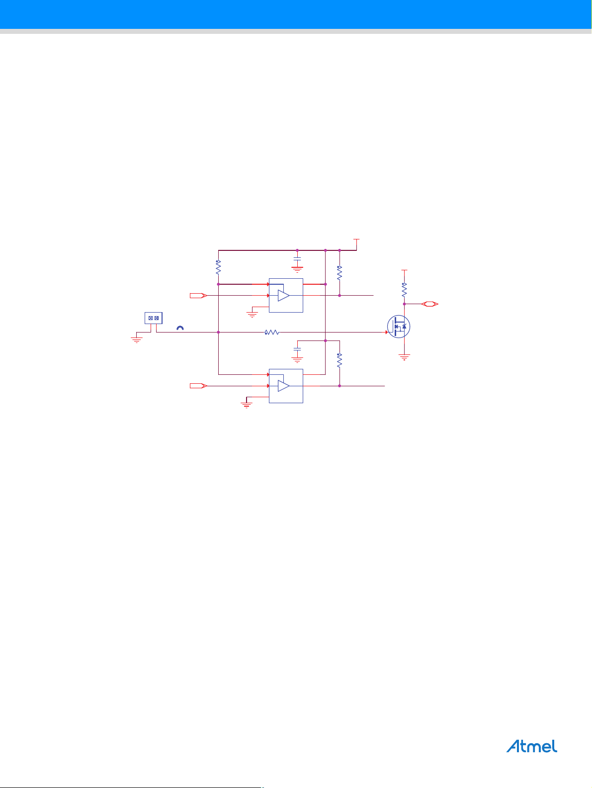
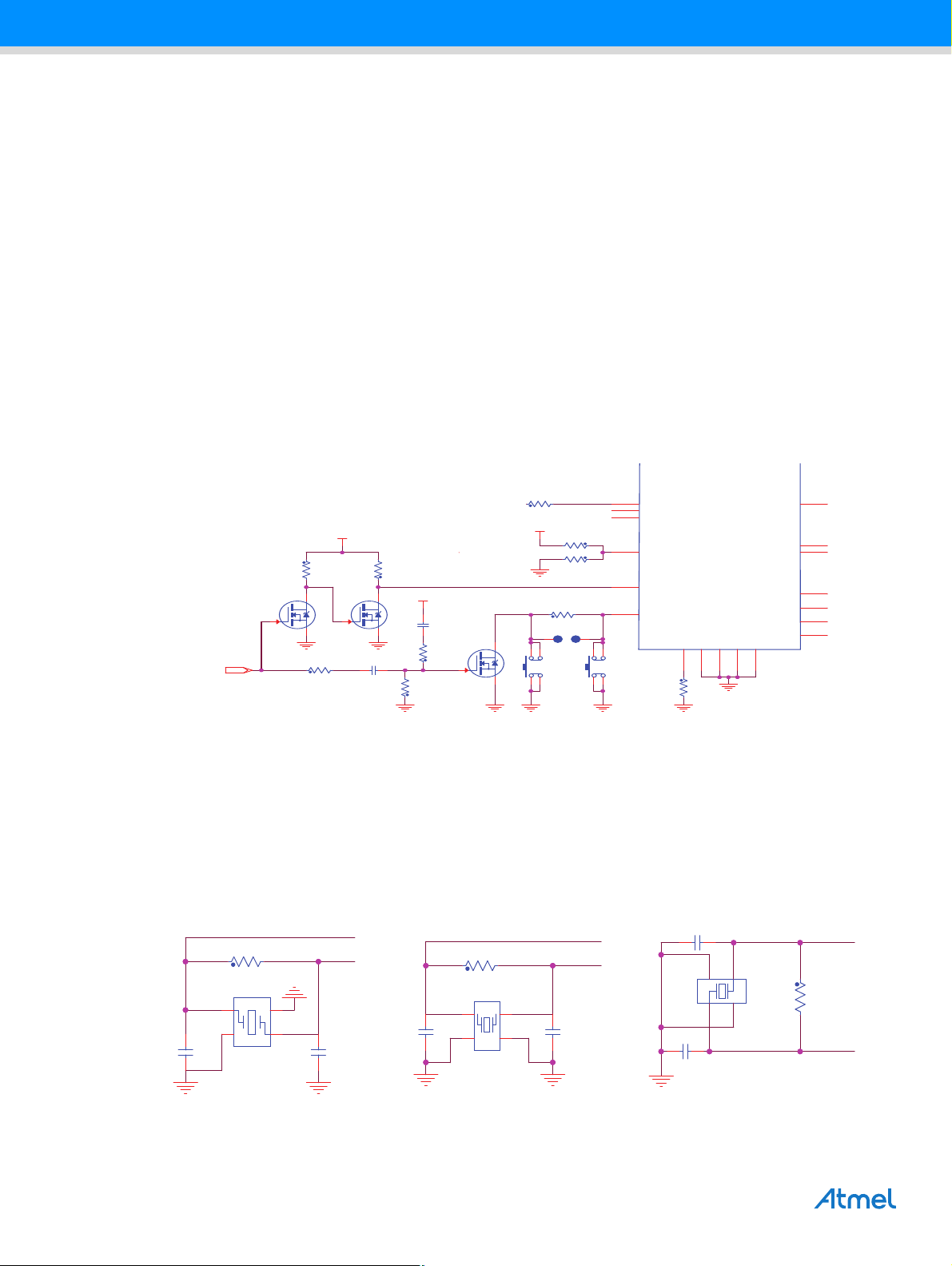
5.3.5.5 CS Disable
BOOT_DIS
QSPI Flash CS
eMMC Flash CS
SPI Flash CS
QSPI0_CS
SPI0_CS0_PA17
VDD_3V3
VDD_3V3
QSPI0_CS_PA23[7]
SPI0_NPCS0_PA17[7]
SDHC0_CD_PA13 [7]
C62
100nF
JPR9
Jumper
VCC
GND
U15
NL17SZ126DFT2G
1
2
3
4
5
Q6
BSS138
1
3
2
R227 100R 1%
VCC
GND
U14
NL17SZ126DFT2G
1
2
3
4
5
JP9
Header 1X2
1
2
R218
10K
C63
100nF
R230
10K
R217
10K
R226
10K
The SAMA5D2 device boots according to the following sequence:
1. SD CARD connected on SDHC1
2. DataFlash connected on NPCS0 SPI0
3. Optional QSPI flash connected on QSPI0 QSPI_CS0
4. eMMC connected to SDHC0
In this sequence, the first device found w ith bootable contents is select ed as the boot source. The ot hers are
disregarded.
On-board jumper (JP9) controls the selection (CS#) of the on-board bootable memory components (eMMC and
Serial DataFlash) using a non-inverting 3- state bu ffe r.
Figure 5-14. CS Disable
The rule of operation is:
JP9 = OFF (default) → enable normal boot from eMMC or serial Flash if mounted
JP9 = ON → booting from optional serial DataFlash or eMMC is disabled
Refer to the SAMA5D2 Series datasheet for more information on standard boot strategies and sequencing.
19
SAMA5D2 Xplained Ultra [USER GUIDE]
Atmel-44028B-ATARM-SAMA5D2-Xplained-Ultra-User Guide_02-Oct-15
5.3.6 Additional Memories
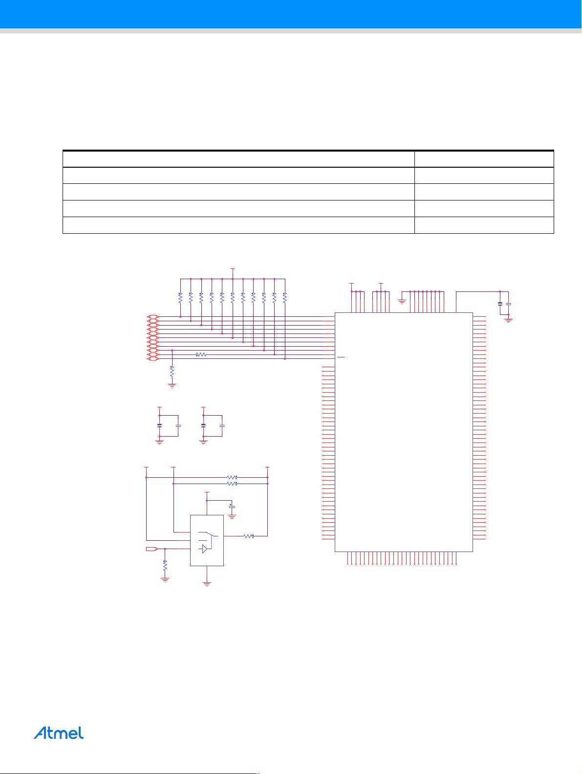
5.3.6.1 Serial Data Flash
The SAMA5D2 provides two high-speed Serial Peripheral Interface (SPI) controllers. One port is used to interface
with the on-board serial DataFlash.
The four main signals used in the SPI are Clock, Data In, Data Out, and Chip Select. The SPI is a serial interface
similar to the I
It operates at a higher speed.
Transmit and receive data lines are separate.
Device access is chip select-based instead of address-based.
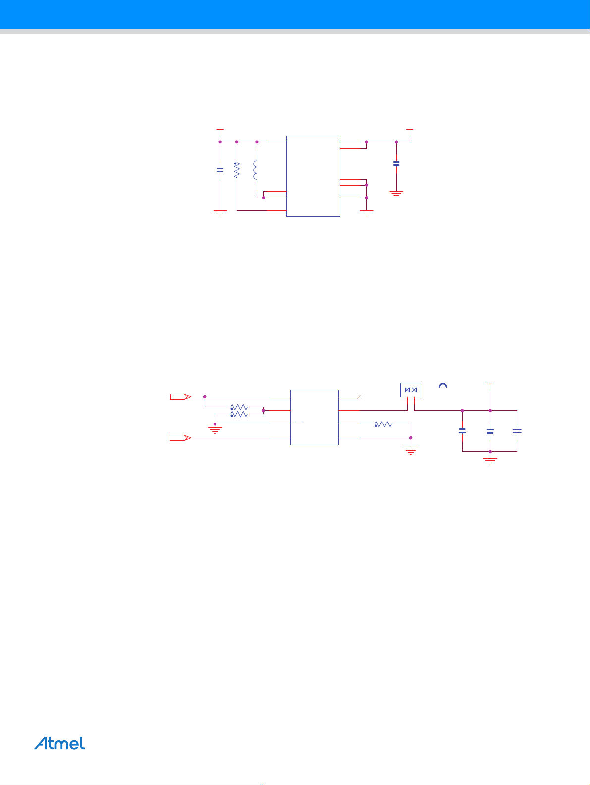
Figure 5-15. Serial DataFlash
2
C bus interface but with three main differences:
5.3.6.2 QSPI Serial Flash
The SAMA5D2 provides two Quad Serial Peripheral Interfaces (QSPI). One port is used to interface with the optional
on-board QSPI serial DataFlash.
The Quad SPI Interface (QSPI) is a synchronous serial data link that provides communication with external
devices in Master mode.
The QSPI can be used in SPI mode to interface to serial peripherals (such as ADCs, DACs, LCD controllers, CAN
controllers and sensors), or in Serial Memory mode to interface to serial Flash memories.
The QSPI allows the system to execute code directly from a serial Flash memory (XIP) without code shadowing to
RAM. The serial Flash memory mapping is seen in the system as other memories (ROM, SRAM, DRAM,
embedded Flash memory, etc.).
SPI0_MOSI_PA15[7]
SPI0_MISO_PA16[7]
SPI0_SPCK_PA14[7]
SPI0_CS0_PA17
5
SI
2
SO
6
SCK
1
CS
AT25DF321A
U9
VCC
WP
HOLD
GND
VDD_3V3
8
3
7
4
C53
100nF
With the support of the Quad SPI protocol, the QSPI allows the system to use high-performance serial Flash
memories which are small and inexpensive, in place of larger and more expensive parallel Flash memories
Figure 5-16. Optional QSPI Se rial DataFlash
VDD_3V3
QSPI0_IO0_PA24[7]
QSPI0_IO1_PA25[7]
QSPI0_IO2_PA26[7]
QSPI0_IO3_PA27[7]
5
2
3
7
DNP(N25Q128A13ESE40F)
U10
DQ0
DQ1
W#/VPP/DQ2
HOLD#/DQ3
VCC
Vss
8
4
1
S#
6
C
SAMA5D2 Xplained Ultra [USER GUIDE]
Atmel-44028B-ATARM-SAMA5D2-Xplained-Ultra-User Guide_02-Oct-15
C52
100nF
QSPI0_CS
QSPI0_SCK_PA22 [7]
20
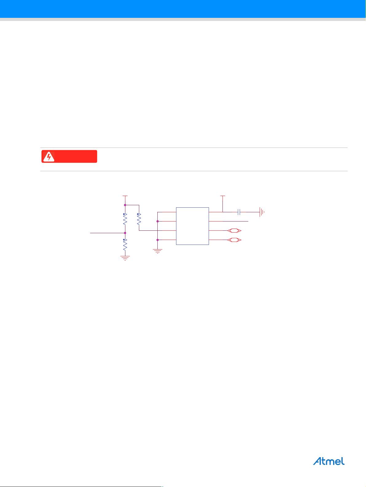
5.3.6.3 Serial EEPROM with Unique MAC Address
WARNING
The SAMA5D2-XULT board embeds one Atmel AT24MAC402/602 EEPROM using a TWI1 interface.
The AT24MAC402/602 provides 20 48 bits of Serial Electrically-Erasable Programmable Read-Only Me mory
(EEPROM) organized as 256 words of eight bits each and is accessed via an I
interface. In addition, the AT24MAC402/602 incorporates an easy and inexpensive method to obtain a globally
unique MAC or EUI address (EUI-48 or EUI-64).
The EUI-48/64 addresses can be assigned as the actual physica l address of a system hardwa re device or node, o r
it can be assigned to a software instance. These addresses are factory-programmed by Atmel and guaranteed
unique. They are permanently write-protected in an extend ed me mor y block located outsid e of the standa rd 2-Kbit
memory array.
In addition, the AT24MAC402/602 provides the value-add ed feature of a factory-program med, also guaranteed
unique 128-bit serial number located in the extended memory block (same area as the EUI address values).
The EEPROM device is used as a “software label” to store board information such as
chip type, manufacture name and production date, using the last two 16-byte blocks in
memory. The information contained in these blocks should not be modified.
Figure 5-17. EEPROM
VDD_3V3 VDD_3V3
R320DNP(10K)
R31910K
EEPROM_WP
R316
0R
U18
1
A0
2
A1
3
A2
4
GND
AT24MAC402-MAHM-T
VCC
WP
SCL
SDA
8
7
6
5
C161 100nF
EEPROM_WP
EEPROM_TWCK1_PD5 [8]
EEPROM_TWD1_PD4 [8]
2
C-compatible (2-wire) serial
21
SAMA5D2 Xplained Ultra [USER GUIDE]
Atmel-44028B-ATARM-SAMA5D2-Xplained-Ultra-User Guide_02-Oct-15
5.4 PIO Usage and Interface Connectors
(MCI1_CD)
(SDHC1_WP)
(MCI1_DA1)
(MCI1_DA0)
(MCI1_CK)
(MCI1_CDA)
(MCI1_DA3)
(MCI1_DA2)
VDD_3V3
VDD_3V3
SDHC1_DAT0_PA18[7]
SDHC1_DAT1_PA19[7]
SDHC1_DAT2_PA20[7]
SDHC1_DAT3_PA21[7]
SDHC1_CMD_PA28[7]
SDHC1_CK_PA22[7]
SDHC1_CD_PA30[7]
R20910K
C75
100nF
R24168K
R19268K
R24568K
R214
0R
J19
SD Card Connector
8
5
7
6
4
3
2
1
9
14
15
16
13
12
11
10
R18968K
R2490R
C64
10uF
R22910K
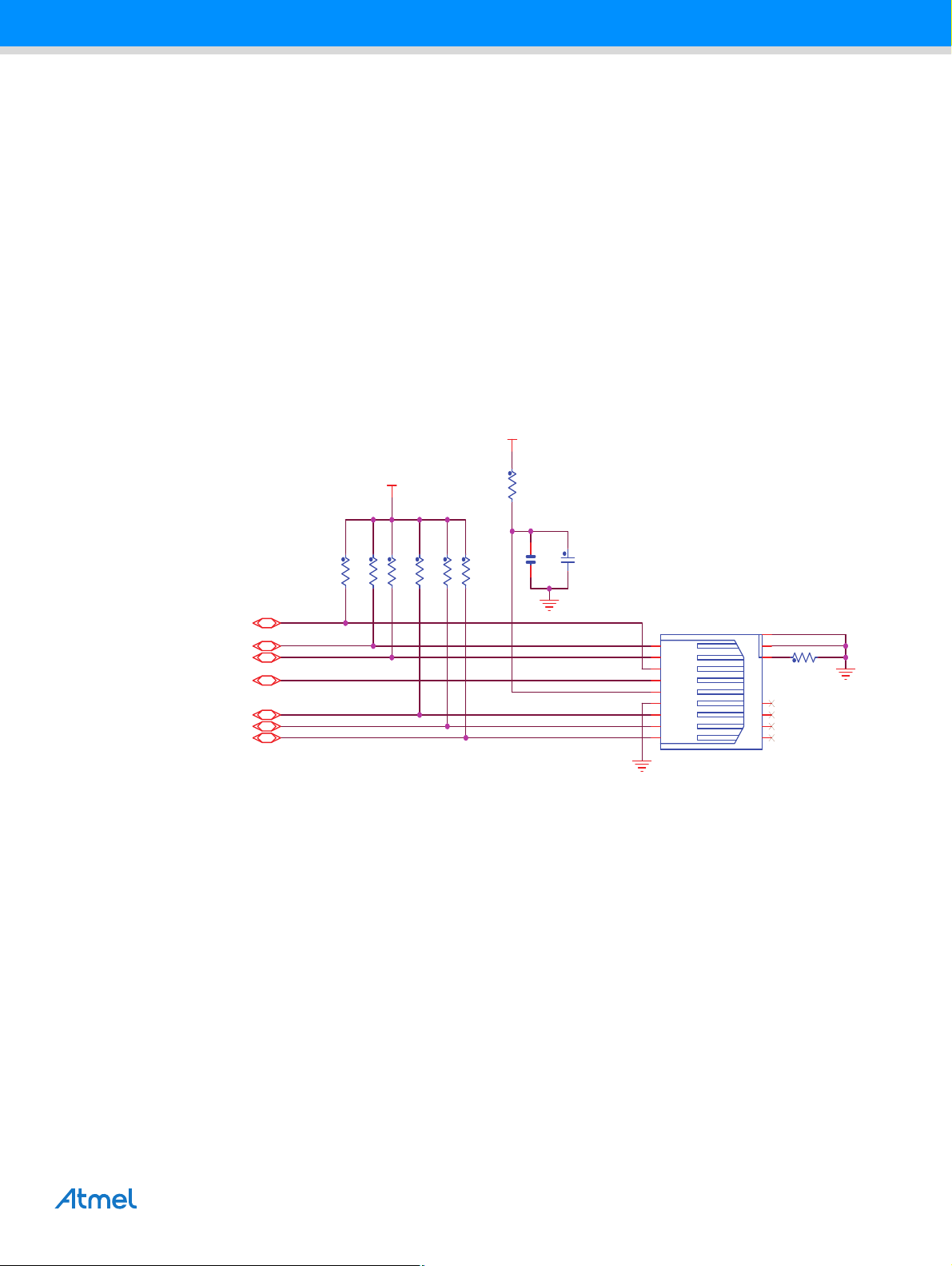
5.4.1 Secure Digital Multimedia Card Interface (SDMMC)
5.4.1.1 Secure Digital Multimedia Card (SDMMC) Controller
The SAMA5D2-XULT board has two Secure Digital Multimedia Card (SDMMC) interfaces that support the
MultiMedia Card (e.MMC) Specification V4.41, the SD Memory Card Specification V3.0, and the SDIO V3.0
specification. It is compliant with the SD Host Controller Standard V3.0 specification.
SDMMC0 interface is connected to the eMMC.
SDMMC1 Interface based on a 7-pin interface (clock, command, 4-bit data, power lines).
5.4.1.2 SDMMC1 Card Connector
A standard MMC/SD card connector, connected to SDMMC1, is mounted on the top side of the board. It includes
a card detection switch.
Figure 5-18. SDMMC1
SAMA5D2 Xplained Ultra [USER GUIDE]
Atmel-44028B-ATARM-SAMA5D2-Xplained-Ultra-User Guide_02-Oct-15
22
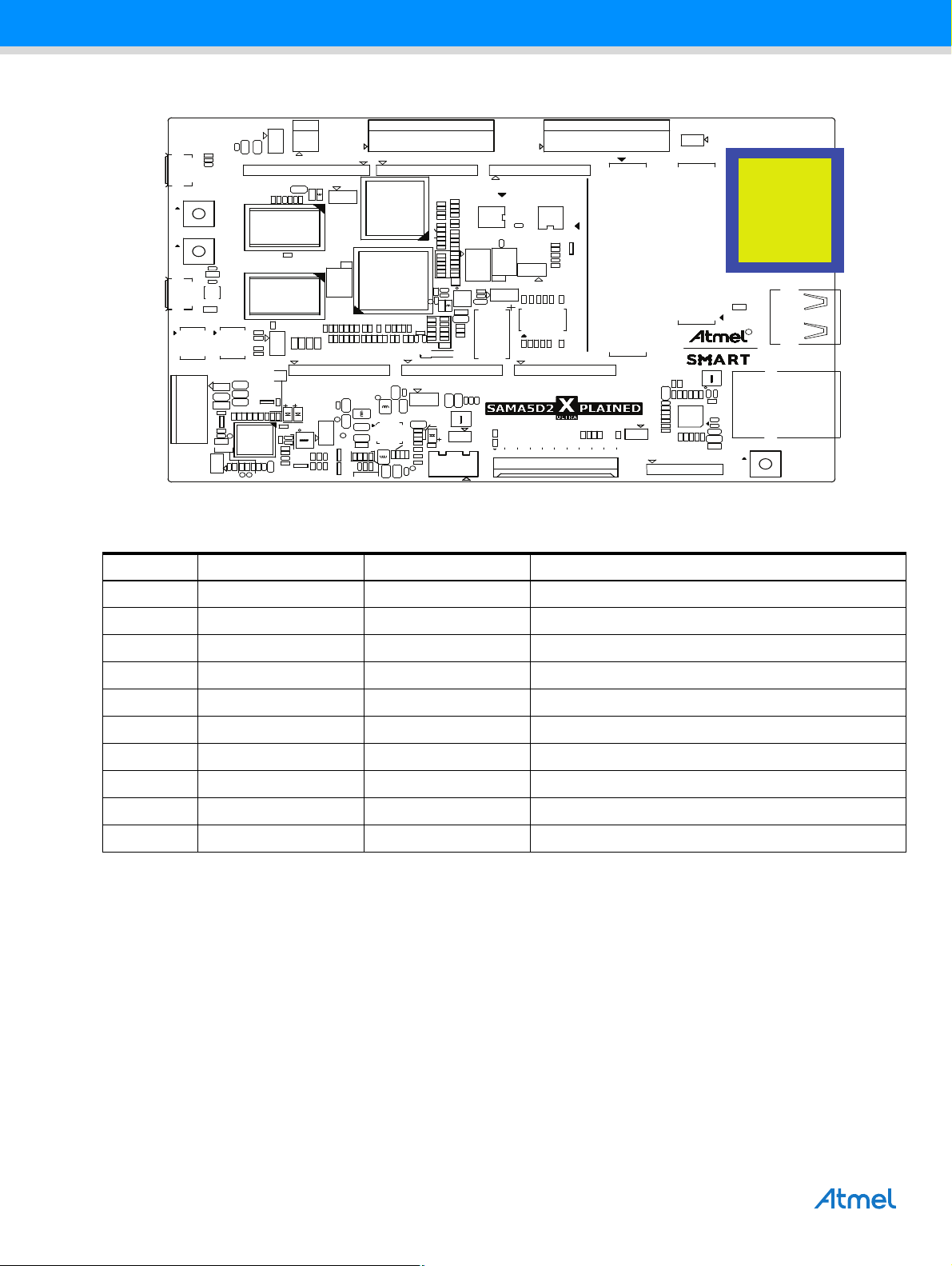
Figure 5-19. Standard SD Socket J19
J10
CLASS D
J5
J23
BP3
BP2
J14
R71
C32
R62
R59
R43
C15
L4
JP1
EDBG_DIS
C58
R184
R183
C57
J20
A5-USB-A
3
42
RESET
3
42
WAKE UP
C50
L13
C49
U5
EDBG-USB
L11
A5-JTAGEDBG-JTAG
R50
Q4
TP4
R2R3R4
C4
R1
TP1 TP2
VDD_5V_IN
J24
JP8
C60
C59
13
GND
AREF
SDA0
SCL0
C56
R181
R180
R179
R178
C55
C54
R104
R99
R75
VDD_3V3
R74
J11
R53
R52
R51
C39
C33
C26
R182
R153
U8
U4
R124
JP5
R58
R57
R56
R55
R54
R5
3V3
VBAT
Q5
R63
STAT
POWER
VDD_3V3_LP
D3
D4
Y1
R46
R29
C14
C11
R12
U1
R25
R23
R8
C9
C5
C6
Q2
R10
XPRO POWER
11
L14
VDDIODDR
R108
L10J7L7L8L9
RST
JP3
R13
C10
R9
C8
J25
XPRO EXT1
7
8
10912
JP7
U11
SDMMC0
U6
A
R128R127
R126R125
R107R106
R102R101
79R89R
R122
R121
R120
R119
R118
R117
R116
R115
R114
R113
R112
R111
R110
R109
R95
R94
R93
R92
R91
R90
R89
R88
R87
R86
R85
R84
R83
R82
5V
3V3
C23
C24
TP6
C20
C17
TP5
C13
L3
Q3
Q1
J8
NC
C38
GND
GND
C37
TP7
L5
L6
VDDCORE
C22
U2
L1
R20
R19
R21
R6
C7
R14
R22
R7
R15
R17
R16
C1
C3
C2
1032456
J21
R176
R174
R172
R170
R168
F4_RXD
F4_TXD
R166
R177
R175
R173
R171
R169
R167
R164
R165
R163
R162
R161
R160
R159
R157
TP8
R131L12
R103
C41
R96
C40
JP4
R44
C19
R41
R30
R27
R24
R18
TP3
R11
J16
R156
B
C48
R139
R138
C45
A2A1A0
R26
JP6
C47
Y4
C46
C44
R129
C43
R123
R105
A
R100
Y3
A6
A5
A4
A3
C28
C27
C31
C29
C30
4
1
D2
3
2
RGB LED
D1
J4
Pin1
J3
VBAT
R151
R149
R147
R144
F1_TXD
J22
B
VDDBU
A7
R42
R28
J26
F1_RXD
XPRO EXT2
17
18
161415
SDA1
F3_RXD
F0_RXD
F3_TXD
F0_TXD
U10
C53
U9
R158
R155
C52
R154
R150
J15
HSIC
R148
R145
R143R142
R141R140
J12
C42
J9
A8
U7
R152
C51
R146
R137
R136
R135
R134
R133
R132
PIOBU
R81
R80
R79
R78
R77
R76
CANRX1
A9
A11
A10
J2
LCD
Table 5-6. Standard SD Socket J19 Signal Descriptions
Pin Mnemonic PIO Signal Description
1DAT3 PA21 Data Bit 3
WWW.ATMEL.COM
JP9
211920
D22
SCL1
D24
D26
D28
D30
D32
D34
D36
D38
D40
D42
DIGITAL
D44
D46
D48
D50
D52
GND
CANTX1
CANRX0
CANTX0
JP2
R40
R39
R36
R37
R38
DEBUG_DIS
BOOT_DIS
V5V5
D23
D25
D27
D29
D31
D33
D35
D37
D39
D41
D43
D45
D47
D49
D51
D53
GND
J17
R73
R72
R66
R65
R68
R67
C36
C25
R61
R60
R49
R48
R47
R45
R31
R32
R33
J1
DEBUG
CTS
RXD VCCTXD
R69
R34
Y2
R70
R35
RTS GND
J19
SDMMC1
ISC
J18
R130
A5-USB-B
R
J13
TM
ETH
C35
C34
R64
J6
U3
C21
C18
C16
C12
L2
PB_USER
3.3V LEVELS
BP1
3
4
2
2 CDA PA28 Command Line
3 GND – Common ground
4 VCC – Supply Voltage 3.3V
5 CLK PA22 Clock / Command Line
6 CD P A30 Card Detect
7DAT0 PA18 Data Bit 0
8DAT1 PA19 Data Bit 1
9DAT2 PA20 Data Bit 2
10 GND – Common ground
23
SAMA5D2 Xplained Ultra [USER GUIDE]
Atmel-44028B-ATARM-SAMA5D2-Xplained-Ultra-User Guide_02-Oct-15
 Loading...