

Atmel SAM9N12/CN11-EK User Manual

SAM9N12/CN11-EK
....................................................................................................................
User Guide
11186A–ATARM–29-Nov-12

Section 1
Introduction.................................................................................................................1-1
1.1 SAM9N12/CN11 Evaluation Kit.......................................................................................... 1-1
1.2 User Guide Content ................................... ... ... ... .... ...................................... .... ... ..............1-1
1.3 References and Applicable Documents............................................................................. 1-1
Section 2
Kit Contents................................................................................................................2-1
2.1 Deliverables ....................................................................................................................... 2-1
2.2 Evaluation Board Specifications......................................................................................... 2-2
2.3 Electrostatic Warning ......................................................................................................... 2-2
Section 3
Power Up....................................................................................................................3-1
3.1 Power up the Board ...................................... ... ... .... ...................................... .... ... ..............3-1
3.2 Battery................................................................................................................................ 3-1
3.3 Sample Code and Technical Support ............................................................................... 3-1
3.4 Recovery Procedure ............................... ... ... ... ... .... ...................................... .... ... .............. 3-1
Section 4
Evaluation Kit Hardware.............................................................................................4-1
4.1 Board Overview................... ... ....................................... ... .... ...................................... ........ 4-1
4.2 Equipment List ................................................................................................................... 4-2
4.2.1 Features List........................................................................................................ 4-2
4.2.2 Interface Connection............................................................................................ 4-3
4.2.3 Configuration Items.............................................................................................. 4-3
4.3 Function Blocks.................................................................................................................. 4-5
4.3.1 Processor............................................................................................................. 4-5
4.3.2 Clock Distribution..... .... ... ....................................... ... ... ....................................... . 4-5
4.3.3 Reset and Wake-up Circuitry............................................................................... 4-6
4.3.4 Power Supplies.................................................................................................... 4-6
4.3.5 Power Rails.......................................................................................................... 4-7
4.3.6 Battery Backup .................................................................................................... 4-8
4.3.7 Memory................................................................................................................ 4-9
4.3.8 UART DBGU...... ... ... ....................................... ... .... ...................................... .... .. 4-10
4.3.9 JTAG Interface................................................................................................... 4-10
4.3.10 Serial Peripheral Interface (SPI) Controller ....................................................... 4-11
4.3.11 Two Wire Interface (TWI)................................................................................... 4-11
4.3.12 USB Ports.................... ... ... ... .... ...................................... .... ... ... ......................... 4-12
4.3.13 1-Wire EEPROM................................................................................................ 4-13
4.3.14 ETH on EBI........................................................................................................ 4-13
SAM9N12/CN11-EK User Guide 1-1
11186A–ATARM–29-Nov-12

4.3.15 Audio.................................................................................................................. 4-14
4.3.16 SD Card....................... ...................................... .... ... ....................................... .. 4-15
4.3.17 ZigBee Interface ................................................................................................ 4-15
4.3.18 Analog Interface ....................................... ... ... ....................................... ... ... ...... 4-16
4.3.19 LED Indicators ................................................................................................... 4-16
4.3.20 Push Buttons ..................... ... .... ...................................... .... ... ............................ 4-17
4.3.21 Expansion Ports................................................................................................. 4-18
4.3.22 PIO Usage ........................................................................................................ 4-19
4.4 Connectors....................................................................................................................... 4-23
4.4.1 Power Supply..................................................................................................... 4-23
4.4.2 JTAG/ICE Connector......................................................................................... 4-23
4.4.3 DBGU ................................................................................................................ 4-24
4.4.4 USB MicroB .................................................... ... .... ... ....................................... .. 4-25
4.4.5 USB Type A port.......... ... ... ....................................... ... ... ................................... 4-25
4.4.6 SD Card MCI ..................... ... .... ... ... ....................................... ... ... ...................... 4-26
4.4.7 Ethernet RJ45 Socket........................................................................................ 4-27
4.4.8 Zigbee Socket J12............................................................................................. 4-27
4.4.9 LCD Socket........................................................................................................ 4-28
4.4.10 IO Expansion Port ............................................................................................. 4-30
Section 5
EK Schematics ...........................................................................................................5-1
5.1 SAM9N12-EK Schematics ................................................................................................. 5-1
5.2 SAM9CN11-EK Schematics............................................................................................... 5-2
Section 6
Display Module Hardware...........................................................................................6-1
6.1 Board Overview................... ... ....................................... ... .... ...................................... ........ 6-1
6.2 Equipment List ................................................................................................................... 6-1
6.3 Function Blocks.................................................................................................................. 6-2
6.3.1 3.3V Regulator...... ... .... ...................................... .... ... ....................................... ... . 6-2
6.3.2 TFT LCD with Touch Panel ................................................................................. 6-2
6.3.3 Back Light............................................................................................................ 6-3
6.3.4 QTouch................................................................................................................ 6-4
6.3.5 1-Wire .................................................................................................................. 6-4
Section 7
DM Schematics...........................................................................................................7-1
7.1 DM Board Schematics ....................................................................................................... 7-1
Section 8
Revision History..........................................................................................................8-1
1-2 SAM9N12/CN11-EK User Guide
11186A–ATARM–29-Nov-12

8.1 Revision History......................................... ... ... ....................................... ... ... ..................... 8-1
SAM9N12/CN11-EK User Guide 1-3
11186A–ATARM–29-Nov-12
1.1 SAM9N12/CN11 Evaluation Kit
This User Guide introduces the SAM9N12 and SAM9CN11 Evaluation Kits and describes their development and debugging capabilities running on S
®
The Atmel
SAM9N12/CN11 Evaluation Kit is a fully-featured evaluation platform for the Atmel
SAM9N12 and SAM9CN11 microcontrollers. The evaluation kit allows users to extensively evaluate,
prototype and create application-spec ific de sig ns.
SAM9N12/CN11 Evaluation Kit consists of two boards:
The Evaluation Kit (EK) board
The Display Module (DM) board
1.2 User Guide Content
This guide gives details on how the SAM9N12/CN11-EK has be en d esigned. I t is mad e up o f 8 sections:
Section 1
Introduction
AM9N12 and SAM9CN11 devices.
Section 1 Introduction (including references, applicable documents)
Section 2 Kit Contents
Section 3 Power Up
Section 4 Evaluation Kit Hardware
Section 5 EK Schematics
Section 6 Display Module Hardware
Section 7 DM Schematics
Section 8 Revision History
1.3 References and Applicable Documents
The documents listed below should be referred for more information on the SAM9CN11-EK.
Table 1-1. Refe
rences and Applicable Documents
Title Comment
SAM9N12/CN11 Datasheet
www.atmel.com
SAM9N12/CN11-EK User Guide 1-1
11186A–ATARM–29-Nov-12
2.1 Deliverables
The Atmel SAM9N12/CN11 Evaluation Kit contains the following items:
Board
– One SAM9N12/CN11-EK board
– One SAM9N12/CN11-DM board
Pow er supply
– Universal input AC/DC power supply with US, Europe and UK plug adapters
– One 3V lithium battery type CR1225
Cables
– One serial RS232 cable
– One micro A/B-type USB cable
– One RJ45 crossed cable
A Welcome letter
Section 2
Kit Contents
Figure 2-1. Unpacked SAM9N12/CN11-EK
SAM9N12/CN11-EK User Guide 2-1
11186A–ATARM–29-Nov-12

Unpack and inspect the kit carefully. Contact your local Atmel distributor, should you have issues concerning the contents of the kit.
2.2 Evaluation Board Specifications
Table 2-1. SAM9N
Characteristics Specifications
Clock speed 400 MHz PCK, 133 MHz MCK
Ports Ethernet, USB, RS232, JTAG, Audio, SD card
Board supply voltage
Temperature
- operating
- storage
Relative humidity 0 to 90% (non condensing)
Dimensions
- SAM9N12/CN11-EK
- SAM9N12/CN11-DM
RoHS status Compliant
2.3 Electrostatic Warning
The SAM9N12/CN11 Evaluation Kit is shipped in a protective anti-static package. The board system
must not be subjected to high electrostatic potentials. We strongly recommend using a grounding strap
or similar ESD protective device when handling the board in hostile ESD environments (offices with synthetic carpet, for example). Avoid touching
board.
12/CN11 Evaluation Kit Specifications
5V DC from connector,
or 5V DC from Micro USB receptacle
-10°C to + 50°C
-40°C to + 85°C
135 mm x 100 mm
135 mm x 70 mm
the component pins
or any other metallic element on the
2-2 SAM9N12/CN11-EK User Guide
11186A–ATARM–29-Nov-12

3.1 Power up the Board
Unpack the board, taking care to avoid el ectrostatic d ischarg e. Unpack t he power supply, sele ct th e right
power plug adapter corresponding to that of your country, and insert it in the power supply.
Section 3
Power Up
Connect the power supply DC connector to the board and plug t
The board LCD should light up and display a graphic demo program. Then, click or touch icons displayed on the screen and enjoy the demo.
3.2 Battery
The SAM9N12/CN11-EK ships with a 3V coin battery.
This battery is not required for the board to start up.
The coin battery is provided for user convenience in case t
time backup function of the SAM9N12/CN11 devices when the board is switched off.
3.3 Sample Code and Technical Support
After boot-up, designers can run sample code or t heir ow n applica tion on the developm ent kit. Users can
download sample code and get technical suppor t from th e Atm el web site : http://www.atmel.com/.
3.4 Recovery Procedure
All boards of Evaluation Kit have passed strict test procedures before shipment. The demo software
boots from SPI DataFlash
the Flash have been deleted, follow the instructions below to recover it to the state as it was when
shipped by Atmel.
®
and stores the binary image in the NAND Flash. If the contents of either of
he power supply to an AC power plug.
he u
ser would like to exercise the date and
Under the web page of SAM9N12/CN11-EK, find the test package of AT91SAM9N12/CN11EK_test_xx_public.zip (xx is the version number), which is the file for Flash content burning. A step-bystep instruction is available in name of SAM9N12/CN11_EK_Test_Software on how to recover the contents and how to make test for each section of the boards.
SAM9N12/CN11-EK User Guide 3-1
11186A–ATARM–29-Nov-12

4.1 Board Overview
This section introduces the Atmel SAM9N12/CN11 Evaluation Kit design. It intr oduces system- level concepts, such as power distribution, memory, and interface assignments.
The SAM9N12/CN11-EK board is built around on the integration of an ARM
(BGA 217 package) with on-board SDRAM, NAND-Flash and a set of popular peripherals. It is designed
to provide a high performance processor evaluation solution with high flexibility for various kinds of
applications.
Figure 4-1. SAM9N12 Board Architecture
Section 43
Evaluation Kit Hardware
®
926-based microcontroller
SAM9N12/CN11-EK User Guide 4-1
11186A–ATARM–29-Nov-12
Figure 4-2. SAM9CN11 Board Architecture
4.2 Equipment List
4.2.1 Features List
Here is the list of the EK board components:
SAM9N12/CN11 microcontroller BGA
– 16 MHz crystal
– 32.768 kHz cry stal
Memory
– 1 Gbit DDR2 memory
– 2 Gbits NAND Flash memor y with chip selection control switch
– Optional NOR Flash
– 32 Mbits SPI serial DataFlash with chip selection control switch
– 512 Kbits serial EEPROM
– 1 Kbit 1-Wire EEPROM
4-2 SAM9N12/CN11-EK User Guide
11186A–ATARM–29-Nov-12

– SD/MMC interface
Communication
– One Ethernet Physical Transceiver Layer with RJ45 connector
– UART DBGU port with level shifter IC
– JTAG/ICE port
– USB Host and Device
–ZigBee
Add-on Display Module
– TFT LCD module with touch screen
–QTouch
Audio CODEC with input stereo headphone and microphone
On-board power regulation and backup battery
Two user LEDs and one power LED
System buttons: NRST, WKUP, OE_CS
One user button
4.2.2 Interface Connection
The SAM9N12/CN11-EK board includes hardware interfaces such as:
DC power supply (J1)
Backup battery (Bt1)
USB host, type A connector (J2)
USB device, micro B connector (J3)
One Ethernet 10/100 interface through an ETH controller (J16)
DBGU (RX and TX only) connected to a 9-way male RS232 connector (J11)
JTAG, 20 pin IDC connector (J4)
SD connector (J8)
Headphone (J13), line-in (J15), on board mic-phone (mic1)
DM board connection for QTouch and TFT LCD display with touch screen and backlight (J9, J10)
ZigBee connector (J12)
Three IO expansion ports (J5, J6, J7)
Test points (various test points are located throughout the board )
®
®
elements for user QTouch: K1 to K4
4.2.3 Configuration Items
Power selection switch (SW1)
Push button - NAND/DataFlash OS_CS (PB1)
Push button - NRST, board reset (PB2)
Push button - Wake-up (PB3)
Push button - PB_USER (PB4)
SAM9N12/CN11-EK User Guide 4-3
11186A–ATARM–29-Nov-12
Figure 4-3. SAM9N12-EK Board Layout
4-4 SAM9N12/CN11-EK User Guide
11186A–ATARM–29-Nov-12
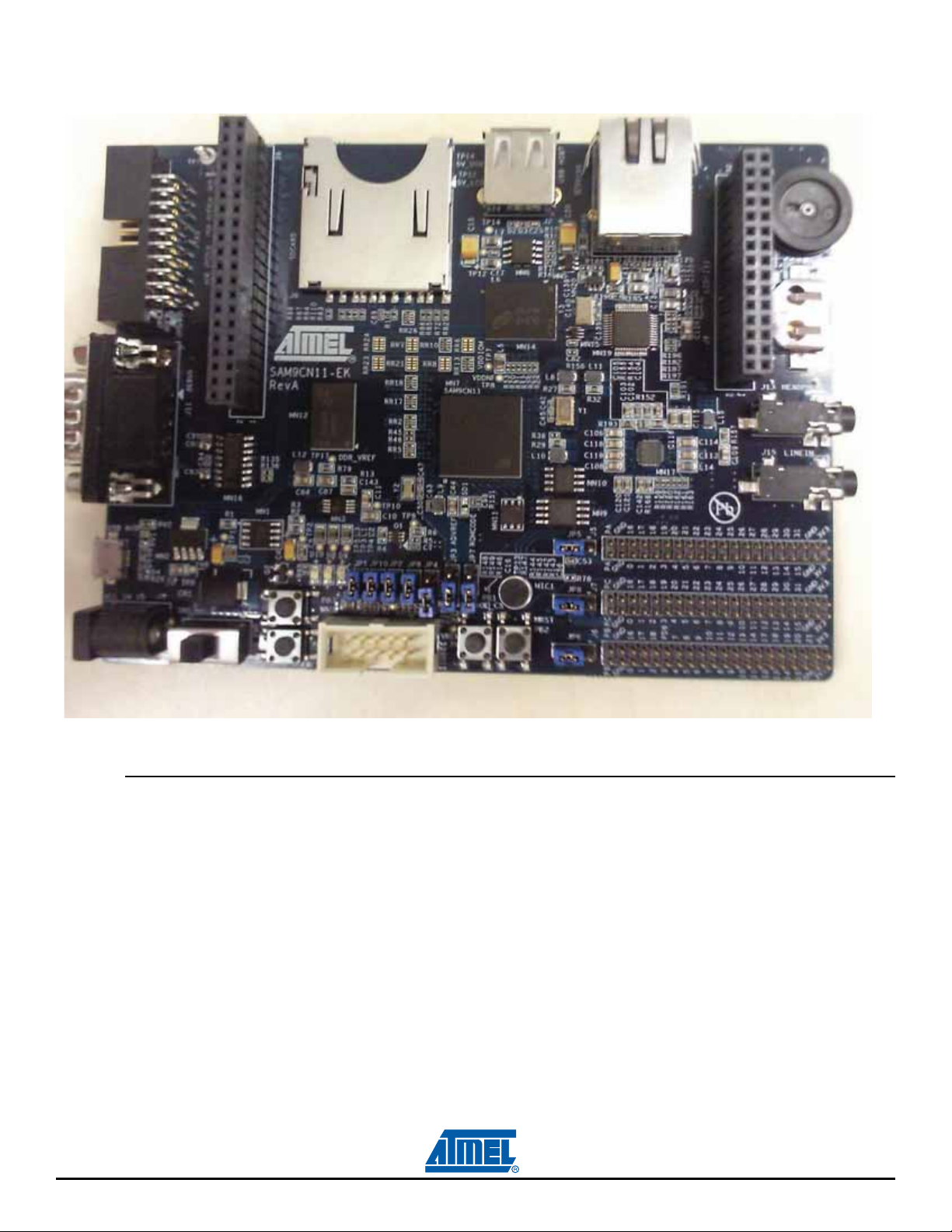
Figure 4-4. SAM9CN11-EK Board Layout
4.3 Function Blocks
4.3.1 Processor
The EK board is equipped with a SAM9N12/CN11 device in BGA2
nominal frequency of 400 MHz for the core and 133 MHz for the system bus.
4.3.2 Clock Distribution
The SAM9N12/CN11-EK board includes three clock systems. Two of the clock systems are alternatives
for the S
AM9N12/CN11 main clock and one clock system is an oscillator used for the Ethernet controller
chip.
SAM9N12/CN11-EK User Guide 4-5
17 package. The processor runs at a
11186A–ATARM–29-Nov-12
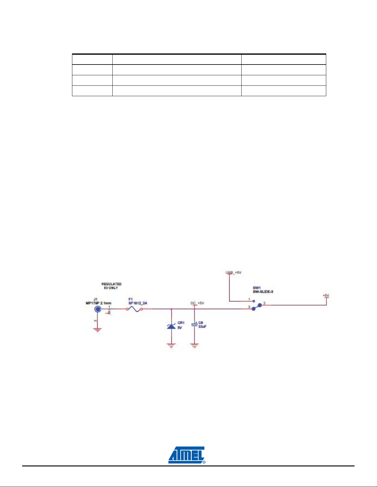
Table 4-1 lists the main components associated with these clock systems.
Tabl
e 4-1. Main Components Associated with the Clock Systems
QTY Description Component assignment
1 Crystal for Internal Clock, 16 MHz Y1
1 Crystal for RTC Clock, 32.768 kHz Y2
1 Crystal for Ethernet Clock, 25 MHz Y3
4.3.3 Reset and Wake-up Circuitry
The reset sources for the EK board are:
Power-on reset
Push-button reset (PB2)
JTAG reset from an in-circuit emulator (JTAG interface is equipped on EK board)
To disable any bootable content in NAND Fl
4.3.4 Power Supplies
The SAM9N12/CN11-EK board evaluation and development platform em beds all the necessary power
ils re
quired for the SAM9N12/CN11 processor and peripherals. The SAM9N12/CN11-EK board can be
ra
supplied by either a USB connection via J3 or a 5V DC block through input J1 (refer to usb schematic).
A manual power supply selection (SW1) between the USB supply a
to select the main power line.
Figure 4-5. Power Input
ash or DataFlash, please refer to “Push Buttons” .
nd the 5V power supply is provided
4-6 SAM9N12/CN11-EK User Guide
11186A–ATARM–29-Nov-12
Connector J1 is provided for use with a DC adapter. I t is a 2.5 mm male po wer jack. Tab le 4-2 below lists
R1
100K
C5
1uF
C3
100nF
TP3
TP4
L2
2 20ohm at 1 00MHz
1 2
L3
2 20ohm at 1 00MHz
1 2
VDDIOP1
TP5
PWR_EN
R2
47K
TP1
R3
15K
+
C1
10uFC21uF
MN1
RT9018A
PGOOD
1
EN
2
VIN
3
VDD
4
NC
5
VOUT
6
ADJ
7
GND8GND
9
+3V3 VDDIOP0
VDDANA
TP2
+
C4
10uF
L1
2 20ohm at 1 00MHz
1 2
+5V
the DC adapter connector pinouts.
Table 4-2. Power Input Configuration
PIN INPUT
1 (Center) Positive
2 No connection
3 (Outside) Ground
4.3.5 Power Rails
The SAM9N12/CN11-EK Board contains three regulated power supplies:
3.3V DC supply
1.8V DC supply
1.0V DC core supply
The outputs of these regulated power supplies are distributed as necessary to the circuits on boards.
The USB supplies and the 5V input DC block are further regulated to 3.3V. The main 3.3V regula tor is
a
sed on a RICHTEK RT9018A low dropout regulator prov iding a fixed output of 3.3V. Its output is used
b
for:
VDDIOP0
VDDIOP1
VDDANA
VDDOSC
VDDUSB
VDDFUSE
When the 3.3V supply is present, power LED D10 is lit.
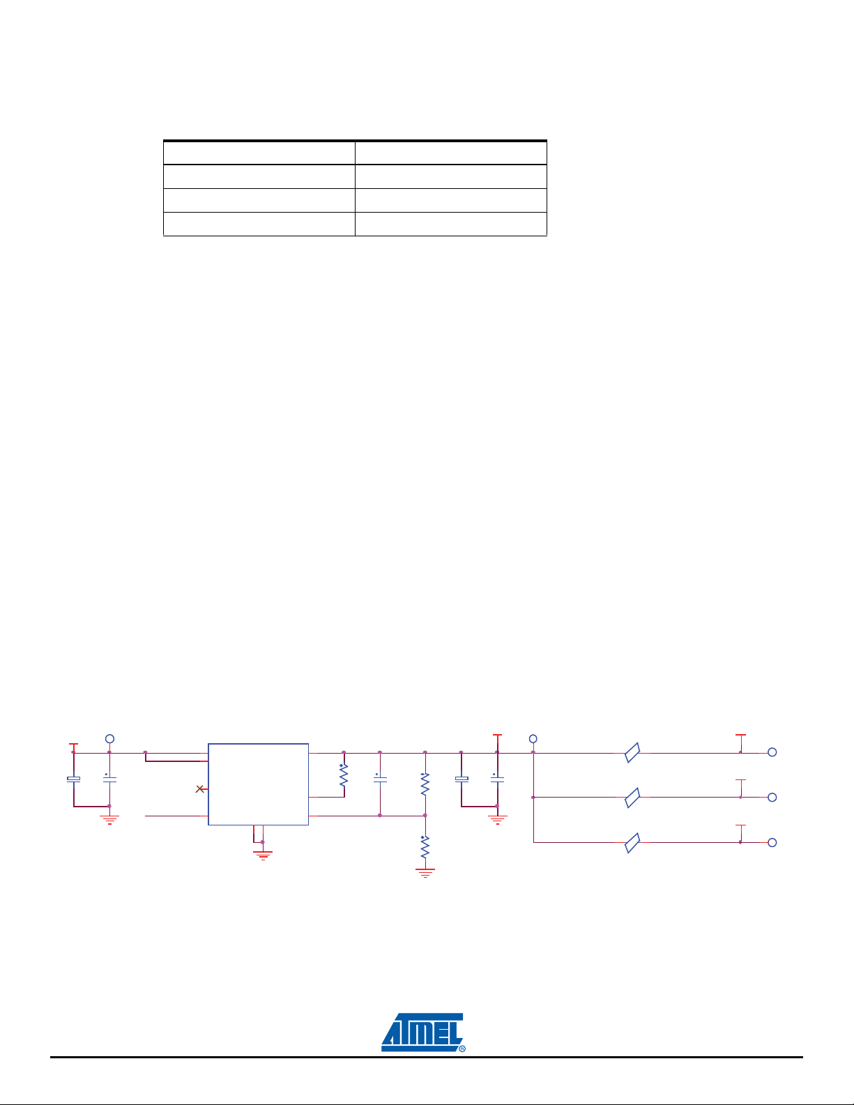
Test points TP2 to TP5 are used to perform testing.
3V Su
pply
11186A–ATARM–29-Nov-12
Figure 4-6. 3.
SAM9N12/CN11-EK User Guide 4-7
The 1.8V DC core supply is based on an LDO LP38692MP IC. It is powered by the 5V DC supply. Its
PWR_EN
TP7
VDDNF
L5
220ohm at 100MHz
1 2
C9
10uF
C8
4.7uF
+5V +1V8
MN2
LP38692MP-1.8
VIN
4
VOUT
3
VEN
1
NC
2
GND
5
VDDIOM
TP6
L4
220ohm at 100MHz
1 2
TP8
JP2
+3V3
BT1
D1
BAT54C
3
2
1
TP13
C18
2.2uF
VDDBU
C16
100nF
output is used for VDDIOM and VDDNF. Test point TP6 is used to perform testing.
Figure 4-7. 1.8V
Supply
The 1.0V DC core supply is based on an LDO ADP1715AR. It is powered by the output of the 3.3V CC
supp
ly. Its output is used for VDDCORE and VDDPLL. Test point TP10 is used to perform testing.
Figure 4-8. 1V Su
+3V3
C10
10uF
pply
C147
22pF
TP10
MN3
1
2
EN
IN
5
ADP1715ARMZ
OUT
ADP1715
ADJ
GND6GND
GND
GND
7
8
3
4
C143
10nf
R13
47K 1%
R10
12 K 1%
C11
10uF
+1V
C144
100nF
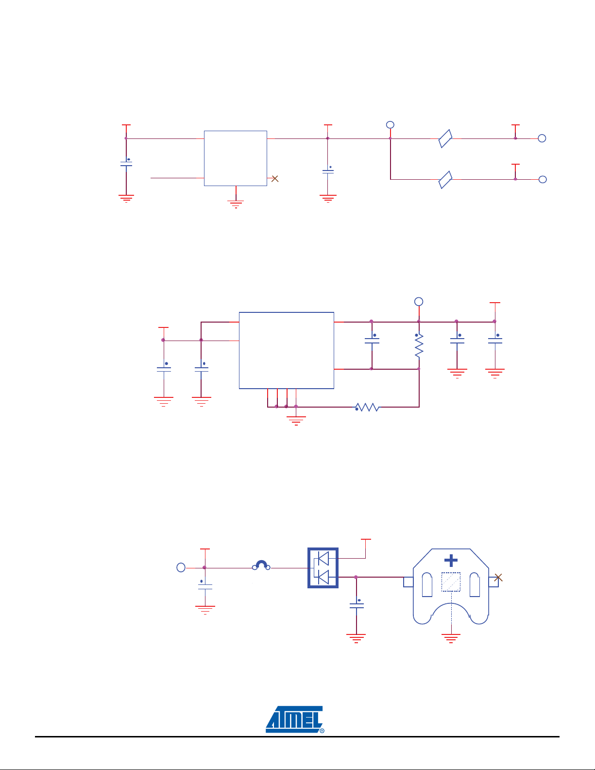
4.3.6 Battery Backup
VDDBU pin is powered from the 3.3V rail and a backup bat
point TP13 and jumper JP2 are used to perform testing.
Figure 4-9. Backup Battery
4-8 SAM9N12/CN11-EK User Guide
11186A–ATARM–29-Nov-12
Note: Test points (TPn) are provided for easy access to each of the regulated power lines.
tery BT1 via a dual Schottky diode D1. Test
4.3.7 Memory
4.3.7.1 DDR2 SDRAM
The SAM9N12/CN11 processor uses DDR2 SDRAM as the system memory. The DDR2 interface uses
1.8V power. The DDR2 chips and SAM9N12/CN11 processor are connected directly. The interface is
1.8V provided by an on-board voltage regulator.
VREF, which is half the interface voltage, or 0.9V, is provide
One 1 Gbit DDR2-SDRAM memory (Micron MT47H64M16HR 8Meg*16*8), 16 bits data interface
connected to D[0-15].
4.3.7.2 NAND FLASH
The SAM9N12/CN11-EK has native support for NAND Flash memory and implements an 8-bit NAND
Flash w
One 2 Gbits NAND Flash (Micro MT29F2G08ABDHC), 16 bits data interface connected to D[0-15].
ith 2 Gbits in size.
4.3.7.3 NOR FLASH
The SAM9N12/CN11-EK provides an optiona
The Flash memory is used with the 16-bit port size.
One reserved position for 128 Mbits NOR Flash (N umonyx JS28F128P30TF75A).
Figure 4-10. External memory
DDR2_D[0..15]
DDR2_A[2..18]
DDR2_SDCKE
DDR2_SDCK
DDR2_NSDCK
DDR2_NCS1
DDR2_CAS
DDR2_RAS
DDR2_SDWE
DDR2_DQS1
DDR2_DQS0
DDR2_DQM1
DDR2_DQM0
C84
4.7uF
+1 V8
L12
10uH/150mA
150mA
R79
1R
C87
4.7uF
C86
100nF
C88
100nF
DDR2_A2
DDR2_A3
DDR2_A4
DDR2_A5
DDR2_A6
DDR2_A7
DDR2_A8
DDR2_A9
DDR2_A10
DDR2_A11
DDR2_A12
DDR2_A13
DDR2_A14
DDR2_A17
DDR2_A18
DDR2_A15
DDR2_A15
R80
1.5K 1%
DDR_VREF
R81
1.5K 1%
M8
M3
M7
N2
N8
N3
N7
P2
P8
P3
M2
P7
R2
L2
L3
L1
K9
K2
J8
K8
L8
L7
K7
K3
B7
A8
F7
E8
B3
F3
A2
E2
R3
R7
R8
MN12
A0
A1
A2
A3
A4
A5
A6
A7
A8
A9
A10
A11
A12
BA0
BA1
BA2
OD T
CKE
CK
CK
CS
CAS
RAS
WE
UDQ S
UDQ S
LD QS
LD QS
UDM
LD M
RFU 1
RFU 2
RFU 3
RFU 4
RFU 5
DDR2 SDRAM
MT47 H 64 M 16 HR
DQ1 0
DQ1 1
DQ1 2
DQ1 3
DQ1 4
DQ1 5
VDDL
VDD Q
VDD Q
VDD Q
VDD Q
VDD Q
VDD Q
VDD Q
VDD Q
VDD Q
VDD Q
VREF
VSSQ
VSSQ
VSSQ
VSSQ
VSSQ
VSSQ
VSSQ
VSSQ
VSSQ
VSSQ
VSSDL
DQ0
DQ1
DQ2
DQ3
DQ4
DQ5
DQ6
DQ7
DQ8
DQ9
VDD
VDD
VDD
VDD
VDD
VSS
VSS
VSS
VSS
VSS
DD R2 SDRAM
TP17
Te s t P o i nt
G8
G2
H7
H3
H1
H9
F1
F9
C8
C2
D7
D3
D1
D9
B1
B9
A1
E1
J9
M9
R1
J1
A9
C1
C3
C7
C9
E9
G1
G3
G7
G9
J2
A3
E3
J3
N1
P9
A7
B2
B8
D2
D8
E7
F2
F8
H2
H8
J7
+1 V8
DDR _VREF
DDR2_D0
DDR2_D1
DDR2_D2
DDR2_D3
DDR2_D4
DDR2_D5
DDR2_D6
DDR2_D7
DDR2_D8
DDR2_D9
DDR2_D10
DDR2_D11
DDR2_D12
DDR2_D13
DDR2_D14DDR2_A16
DDR2_D15
OE_Dataflash
C79
100 nF
C61 100nF
C62 100nF
C63 100nF
C64 100nF
C65 100nF
C66 100nF
C67 100nF
C70 100nF
C71 100nF
C72 100nF
C73 100nF
C74 100nF
C75 100nF
C76 100nF
C77 100nF
C78 100nF
VDDI OP0
NAN D CS
R54
10K
3
d by a simple voltage divider of 1.8V.
l 128 Mbits of Flash memory using a chip-select signal.
FLASH_D[0..15]
OE_Nandflash
+1V8
21
D11
BAT54C
R156
10K
FL A SH _A[ 1 .. 23 ]
NOR_NRST
NCS0
NRD
NWR E
NAND_FSH_D[0..7]
NANDR_B
MN15
NL17SZ126
OE1VCC
2
IN
3
GN D
OE_Nandflash
PB1
3
4 2
FLASH_A1
FLASH_A2
FLASH_A3
FLASH_A4
FLASH_A5
FLASH_A6
FLASH_A7
FLASH_A8
FLASH_A9
FLASH_A10
FLASH_A11
FLASH_A12
FLASH_A13
FLASH_A14
FLASH_A15
FLASH_A16
FLASH_A17
FLASH_A18
FLASH_A19
FLASH_A20
FLASH_A21
FLASH_A22
FLASH_A23
+1 V8
R70 0R
R71 100K
VDDN F
VDDN F
+1V8
NANDCLE
NANDALE
NANDOE
NANDWE
C82
100 nF
R72 100K
R73 470K
R165 DNP
R74 470 K
R75 470 K
R76 470 K
R77
DNP
JP9
PD6
5
4
OUT
1
29
25
24
23
22
21
20
19
8
7
6
5
4
3
2
1
55
18
17
16
11
10
9
45
44
15
30
32
14
43
R166
DNP
D5
C4
D4
C7
C6
CE
C8
RB
C3
WP
G5
A1
A2
A9
A10
B1
B9
B10
D6
D7
D8
E3
E4
E5
E6
E7
E8
F3
F4
F5
F6
F8
G3
G8
L1
L2
MN 1 3
A1
A2
A3
A4
A5
A6
A7
A8
A9
A10
A11
A12
A13
A14
A15
A16
A17
A18
A19
A20
A21
A22
A23
CLK
RST#
WP#
CE#
OE#
WE#
VPP
JS28F128P30TF75A
RFU1
RFU2
VCCQ
DQ1 0
DQ1 1
DQ1 2
DQ1 3
DQ1 4
DQ1 5
WAIT
ADV#
DQ0
DQ1
DQ2
DQ3
DQ4
DQ5
DQ6
DQ7
DQ8
DQ9
NC
VCC
VSS
VSS
VSS
NOR FLASH (DNP)
MN14
CLE
ALE
RE
WE
CE
R/ B
WP
LOC K
N. C1
N. C2
N. C3
N. C4
N. C5
N. C6
N. C7
N. C8
N. C9
N. C10
N. C11
N. C12
N. C13
N. C14
N. C15
N. C16
N. C17
N. C18
N. C19
N. C20
N. C21
N. C22
N. C23
N. C24
N. C25
MT29F2G08ABDHC:D
NAND FLA SH
MT29F2G08ABD
VFBGA-63
N.C26
N.C27
N.C28
N.C29
N.C30
N.C31
N.C32
N.C33
N.C34
N.C35
N.C36
N.C37
N.C38
N.C39
I/O 0
I/O 1
I/O 2
I/O 3
I/O 4
I/O 5
I/O 6
I/O 7
VCC
VCC
VCC
VCC
VSS
VSS
VSS
VSS
NAND FLASH
34
FLASH_D0
36
FLASH_D1
39
FLASH_D2
FLASH_D3
41
FLASH_D4
47
49
FLASH_D5
51
FLASH_D6
FLASH_D7
53
FLASH_D8
35
37
FLASH_D9
40
FLASH_D10
FLASH_D11
42
FLASH_D12
48
50
FLASH_D13
52
FLASH_D14
54
FLASH_D15
56
46
26
27
13
33
38
C68
12
100n F
28
31
H4
NAND_FSH_D0
NAND_FSH_D1
J4
NAND_FSH_D2
K4
K5
NAND_FSH_D3
K6
NAND_FSH_D4
J7
NAND_FSH_D5
NAND_FSH_D6
K7
J8
NAND_FSH_D7
H3
J3
H5
J5
H6
G6
H7
G7
L9
L10
M1
M2
M9
M10
VDDNF
D3
G4
H8
J6
C5
F7
K3
K8
+1V8
C80100nF
C81100nF
C83100nF
C85100nF
C69
100n F
SAM9N12/CN11-EK User Guide 4-9
11186A–ATARM–29-Nov-12
A 3-state buffer is in serial with NAND flash’s CE signal, with PB1 to give a manually disable manner for
NAND boot.
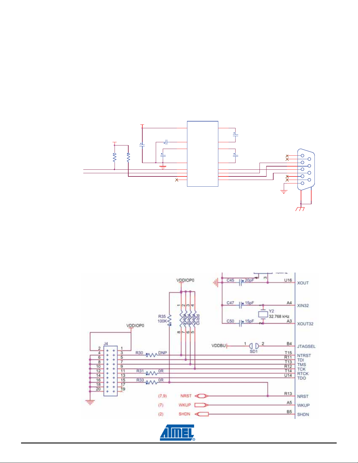
4.3.8 UART DBGU
The Universal Asynchronous Receiver Transmitter features a two-pin UART that can be used for communication and trace purposes and offers an ideal medium for in-situ programming solutions.
This two-pin UART (TXD and RXD only) is buffered throu gh an RS232 transceiver MN16 and brought to
DB9 male connector J11.
the
Figure 4-11. UART
MN 16
VDDI OP0
R135
100K
PA10
(D TXD )
PA9
(DRXD)
R136
100K
VDD I OP0
C92
100 nF
C90
100nF
C93
100nF
MAX323 2CSE
16
VCC
2
V+
6
V-
15
GND
11
T1IN
12
R1OUT
10
T2IN
9
R2OUT
UART
C1+
C2+
T1OU T
R1IN
T2OU T
R2IN
C1-
C2-
1
C91
3
4
5
14
13
7
8
100nF
C94
100nF
J11
1
6
2
7
3
8
4
9
5
10
11
4.
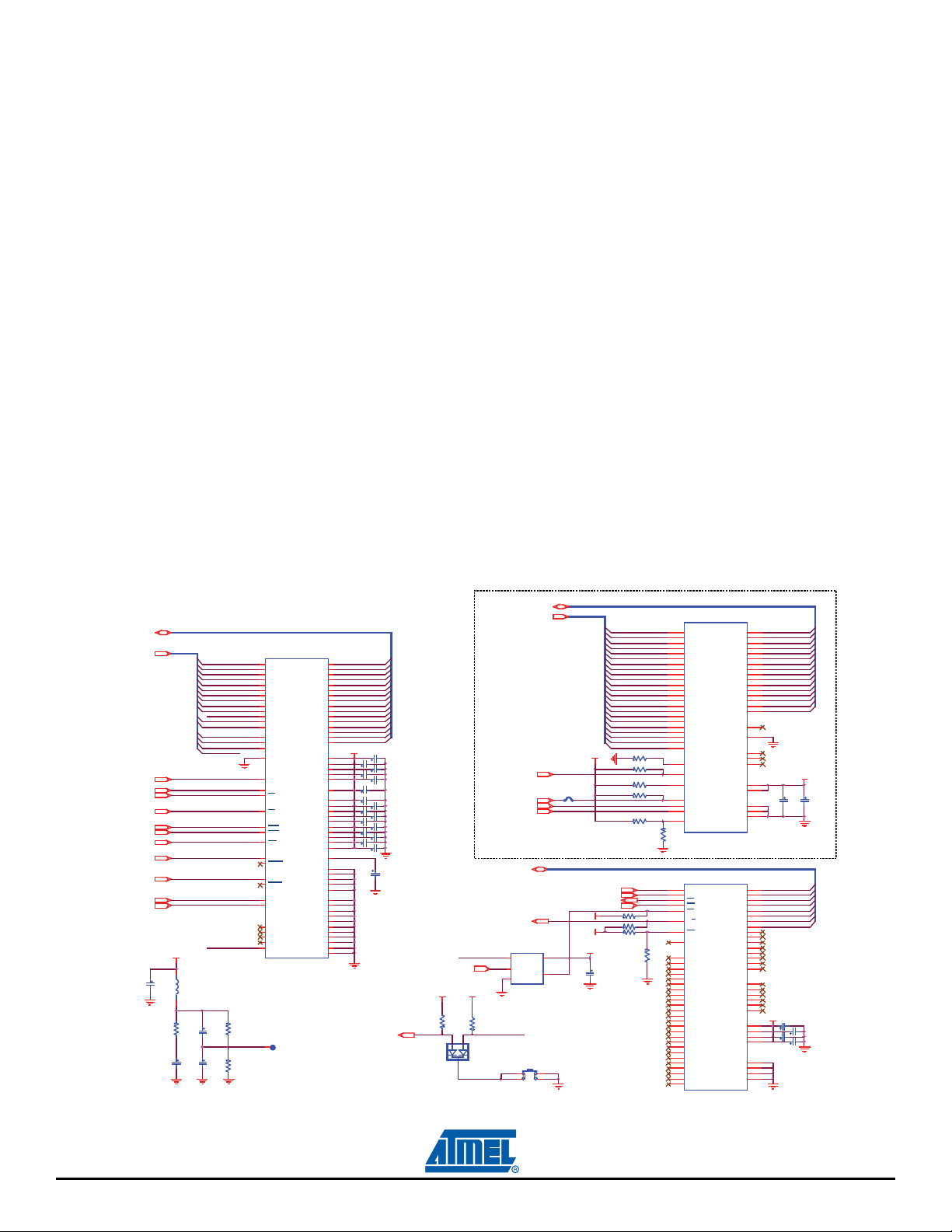
3.9 JTAG Interface
The SAM9N12/CN11-EK board includes a JTAG interface port (J4), to provide deb ug level access t o the
ocessor. The JTAG port is a 20-pin male connector. This port provides the required interface for in-cir-
pr
cuit emulators such as ARM’s Multi-ICE.
Figure 4-12. JTAG
4-10 SAM9N12/CN11-EK User Guide
11186A–ATARM–29-Nov-12
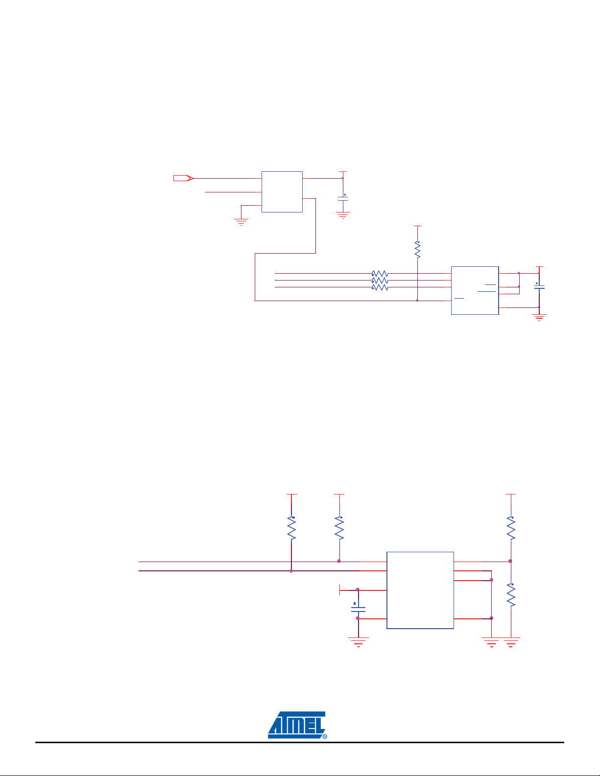
4.3.10 Serial Peripheral Interface (SPI) Controller
R56 0R
R57 0R
R58 0R
VDDIOP0
VDDIOP0
MN9
AT25DF321A
HOLD
7
GND
4
VCC
8
CS
1
SCK
6
SI
5
SO
2
WP
3
PA12
PA11
(SPI0_MOSI)
(SPI0_MIS0)
(SPI0_SPCK)
(SPI0_NPCS0)
C59
100nF
R55
470K
OE_Dataf lash
VDDIOP0
PA14
C58
100nF
MN8
NL17SZ126
OE1VCC
5
GND
3
OUT
4
IN
2
PA13
MN10
AT24C512C-SSHD-T
A0
1
A1
2
WP
7
SCL
6
VCC
8
A3
3
SDA
5
GND
4
VDDIOP0
R61
10K
VDDIOP0VDDIOP0
PA31
PA30
(TW DO)
(TW CKO)
R59
4.7K
VDDIOP0 R62
DNP
R60
4.7K
C60
100nF
The SAM9N12/CN11 serial processor provides two high-speed Serial Peripheral Interface (SPI) controllers. One port is used to interface with the on-board serial DataFlash.
A 3-state buffer is in serial with DataFlash CS signal, with PB1 to give a manually disable manner for
Flash boot.
Data
Figure 4-13. SPI DataFlash
4.3.
11 Two Wire Interface (TWI)
The SAM9N12/CN11 processor has two full speed (400 kHz) master/slave I2 C serial controllers. The
rollers are fully compatible with the industry standard I2C interfaces. On the EK board, TWI0 port is
cont
used to interface with serial EEPROM, QTouch device and audio CODEC interface.
SAM9N12/CN11 processor supports TWI EEPROM boot at the device
address of 0x50. On board, the
EEPROM device address is 0x51. Customer needs to dismount R61 and mount R62 as 10 kohms, if
EEPROM boot is needed.
Figure 4-14. EEPROM
SAM9N12/CN11-EK User Guide 4-11
11186A–ATARM–29-Nov-12
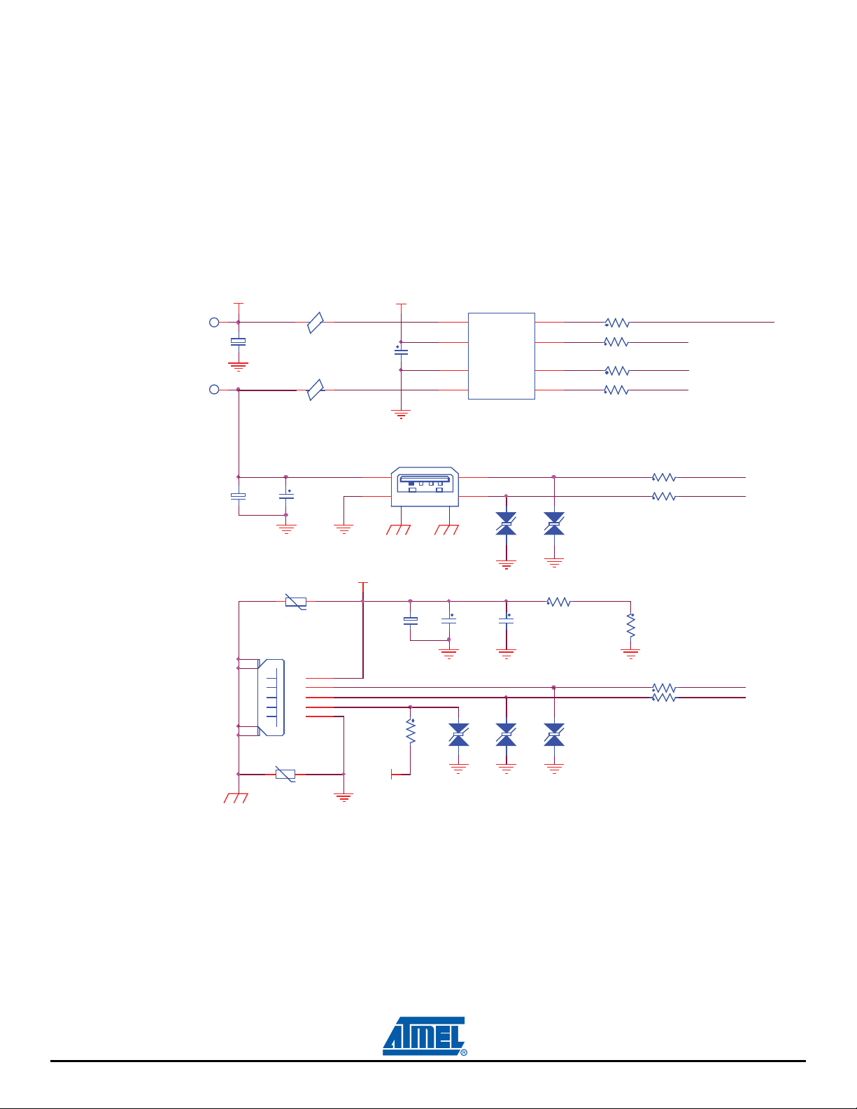
4.3.12 USB Ports
TP12
+5V
+
C37
10uF
C32
10pF
D6
TVS
1
2
D5
TVS
1
2
R16 0R
R17 0R
R18 0R
R19 0R
D4
TVS
1
2
USB_A
J2
USB-AF-4
1
4
5
2
3
6
USB_+5V
PC31
RV1
V5.5MLA0603
PB8
VBUS
SHD
DM
DP
ID
GN D
J3
USB Micro B
1
2
3
4
5
7
6
8
9
C31
100nF
R21 27R
R20 27R
R24 27R
R25 27R
R26
47K
MN6
SP2526A-2
ENA
1
FLGA
2
ENB
4
OUTA
8
GNG6FLGB
3
IN
7
OUTB
5
D2
TVS
1
2
PB7
L7
220ohm at 100MH z
1 2
R22 47K
C17
100nF
L6
220ohm at 100MH z
1 2
+5V_LCD
D3
TVS
1
2
R23
68K
+3V3
TP14
RV2
V5.5MLA0603
+
C15
33uF
PB16
+
C20
33uF
C25
100nF
The SAM9N12/CN11-EK features two full speed (OHCI) USB ports:
Host full speed, type A USB receptacle, J2
Device full speed, micro B USB receptacle, J3
SAM9N12/CN11-EK features USB power function from device
port J3. SW1 functions as switch
between USB supply and DC input jack J1.
The USB host ports are equipped with 500 mA power switch for bus-powered applications.
Figure 4-15. USB Port
4-12 SAM9N12/CN11-EK User Guide
11186A–ATARM–29-Nov-12
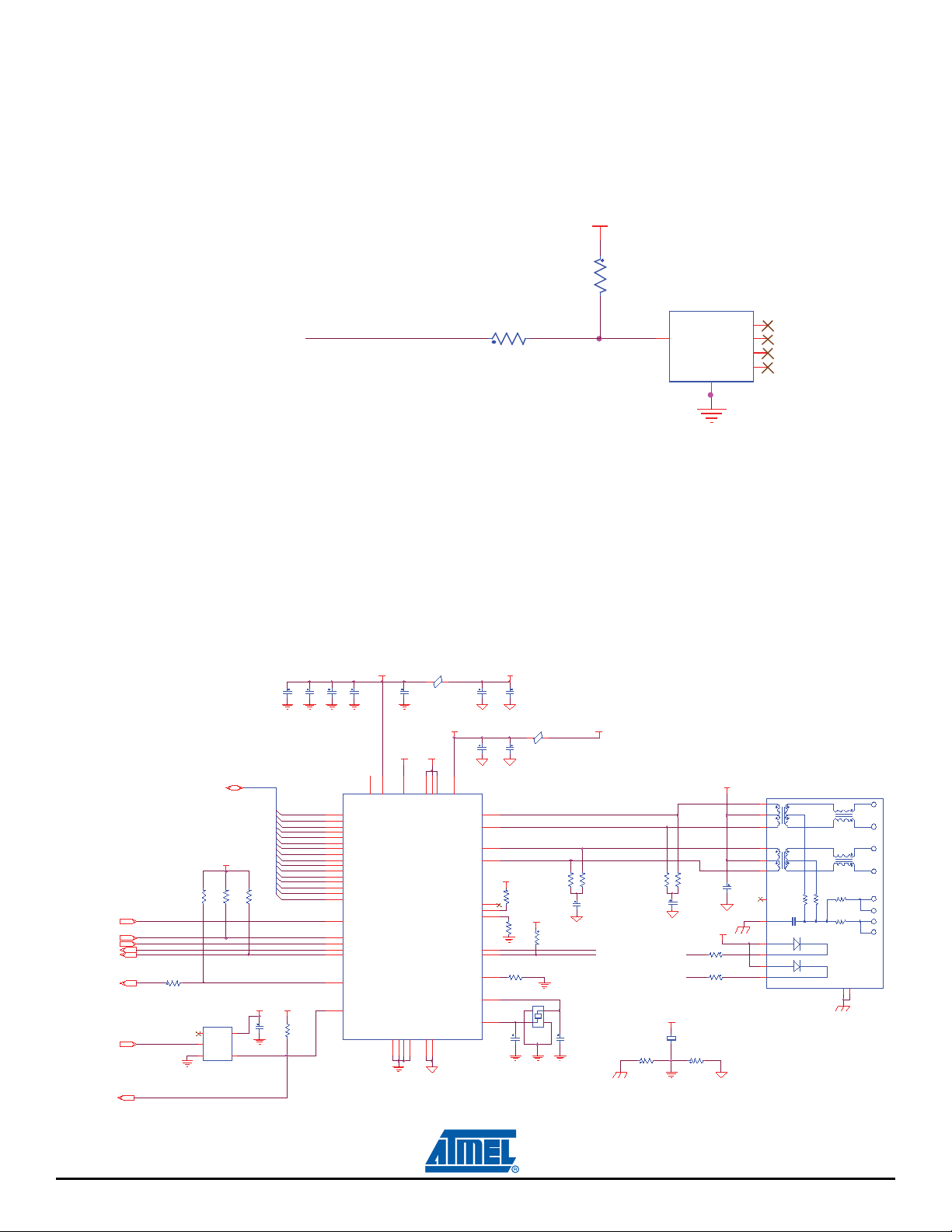
4.3.13 1-Wire EEPROM
MN11
DS2431P+
IO
2
GND
1
NC1
3
NC2
4
NC3
5
NC4
6
VDDIOP0
R65 0R
PA4
R64
1.5K
The SAM9N12/CN11 Evaluation Kit uses 1-Wire device as “soft label” to store the information such as
chip type, manufacture’s name, production date, etc.
Figure 4-16. 1-Wir
4.3.14 ETH on EBI
The SAM9N12/CN11 Evaluation Kit uses EBI-based 8-bit EMAC controller KSZ8851 to implement a
10/10
status LEDs.
For more information about the Ethernet controller device, refer to the Micrel KSZ8851 manufacturer's
data
e
0 Ethernet access. The board integrates an RJ45 connector with embedded transformer, and two
sheet.
Figure 4-17. Ethernet
VDD_D1.8
7
C130
10 0nF
A1V8
14
VD D_ A 1. 8
DGND26AGND13AGND
DGND28DGND
DGND
37
L22
220 ohm at 100 MHz
1 2
+1 V 8
27
46
VDD_IO
VDD_IO38VD D_ I O
18
GND_ETH
A3V3
A1V8
C131
C132
100nF
4.7 uF
GND_ ETHGND_ ETH
L23
220 ohm a t 100 MHz
1 2
C133
C134
100nF
10u F
GND_ ETH
GND_ ETH
21
19
TXP1
VD D_ A 3. 3
20
TXM 1
16
RXP1
17
RXM1
+1 V 8
49 .9R 1%
R183
DNP
15
EECS
10
EESK
9
EE D _ I O
P1 L E D 0
P1 L E D 1
ISET
X1
X2
R196
1K
2
1
22
R185 3.01K 1%
24
25
C139
22p F
+1V8
R197
4.7K
Y3
1234
25M Hz
+3 V3
A3V3
J16
J00 -00 61
1
TD+
4
CT
2
TD-
3
RD+
5
CT
6
R177
R 176
49. 9R 1%
C136
100 nF
GND_ ETH
P1LED0
P1LED1
C140
22p F
R178
49. 9R 1%
R189
0R
GND _ETH
+1V8
+
C137
10 0nF
C141
10 uF
R179
49. 9R 1%
P1LED0
P1LED1
R190
0R
GND_ ETH
R184
470 R
R186
470 R
GN D_ETH
+3V3
RD-
C135
10u F
7
8
9
10
12
11
7575
NC
1nF
1
TX +
2
TX -
3
RX +
6
RX -
75
4
5
75
7
8
13
14
11186A–ATARM–29-Nov-12
ET H _D [ 0. . 15 ]
+1V8
R182
R181
R180
47K
47K
DN P
A1
PD19
NW RE
NR D
PD21
PD20
NR ST
NOR_NRST
R 187 22R
MN20
SN 74LVC 1G07
1
N.C.
2
A
GND3Y
+3V3
C138
5
VCC
100 nF
4
C127
C126
100 nF
10 uF
ETH_D0
ETH_D1
ETH_D2
ETH_D3
ETH_D4
ETH_D5
ETH_D6
ETH_D7
ETH_D8
ETH_D9
ETH_D10
ETH_D11
ETH_D12
ETH_D13
ETH_D14
ETH_D15
+1V8
R188
4. 7K
C 128
1 00n F
48
47
45
44
43
42
41
40
39
36
35
34
33
32
31
30
11
12
6
5
4
3
23
MN19
SD0
SD1
SD2
SD3
SD4
SD5
SD6
SD7
SD8
SD9
SD10
SD11
SD12
SD13
SD14
SD15
CMD
CSN
WRN
RDN
INTRN
PME
RSTN
C129
10 0nF
+1 V 8
8
29
VD D_ C O 1 . 8
KSZ8 851-1 6MLL
SAM9N12/CN11-EK User Guide 4-13
 Loading...