

Page 1

SAM9G15-EK
SAM9G25-EK
SAM9G35-EK
SAM9X25-EK
SAM9X35-EK
...................................................................................................................
User Guide
11115A–ATARM–27-Jul-11
Page 2

1-2 Evaluation Kit (EK) User Guide
11115A–ATARM–27-Jul-11
Page 3

Section 1
Introduction.................................................................................................................1-1
1.1 Scope................................................................................................................................. 1-1
1.2 Applicable Documents ....................................................................................................... 1-2
Section 2
Kit Contents ................................................................................................................2-1
2.1 Deliverables ....................................................................................................................... 2-1
2.2 Evaluation Board Specifications......................................................................................... 2-2
2.3 Electrostatic Warning .........................................................................................................2-3
Section 3
Power Up....................................................................................................................3-1
3.1 Power Up the Board........................................................................................................... 3-1
3.2 DevStart ............................................................................................................................. 3-1
3.3 Recovery Procedure .......................................................................................................... 3-2
3.4 Sample Code and Technical Support ................................................................................ 3-2
Section 4
Evaluation Kit Hardware .............................................................................................4-1
4.1 Introduction ........................................................................................................................ 4-1
4.2 Computer Module (CM)...................................................................................................... 4-3
4.2.1 CM Board Overview ............................................................................................. 4-3
4.2.2 Equipment List ..................................................................................................... 4-3
4.2.3 Function Blocks ................................................................................................... 4-5
4.2.4 Configuration ..................................................................................................... 4-14
4.2.5 Connectors ........................................................................................................ 4-15
4.2.6 Schematics ........................................................................................................ 4-16
4.3 EK Board Description....................................................................................................... 4-21
4.3.1 EK Board Overview ........................................................................................... 4-21
4.3.2 Equipment List ................................................................................................... 4-22
4.3.3 Function Blocks ................................................................................................. 4-23
4.3.4 Configuration ..................................................................................................... 4-39
4.3.5 Connectors ........................................................................................................ 4-45
4.3.6 Schematics ........................................................................................................ 4-63
4.4 Optional Display Module (DM) Board Hardware .............................................................. 4-78
4.4.1 DM Board Overview ........................................................................................... 4-78
4.4.2 Equipment List ................................................................................................... 4-78
4.4.3 Function Blocks ................................................................................................. 4-78
Evaluation Kit (EK) User Guide i
11115A–ATARM–27-Jul-11
Page 4

4.4.4 Schematics ........................................................................................................ 4-82
Section 5
Revision History..........................................................................................................5-1
5.1 Revision History ................................................................................................................. 5-1
ii Evaluation Kit (EK) User Guide
11115A–ATARM–27-Jul-11
Page 5

1.1 Scope
Section 1
Introduction
This User Guide introduces the Evaluation Kit and describes the development and debugging capabilities running on an AT91SAM9 ARM®-based Embedded MPUs as listed below:
SAM9G15
SAM9G25
SAM9X25
SAM9G35
SAM9X35
The User Guide pertains to the following Evaluation Kit references:
SAM9G15-EK
SAM9G25-EK
SAM9X25-EK
SAM9G35-EK
SAM9X35-EK
This User Guide gives design details on the Evaluation Kit and is made up of 5 sections:
Section 1 includes a photo of the board, device and kit references and applicable documents.
Section 2 describes the kit contents, its main features.
Section 3 provides instructions to power up the Evaluation Kit and describes how to use it.
Section 4 describes the CPU Module (CM), the Main Board (MB) and optional Display Module (DM).
Evaluation Kit (EK) User Guide 1-1
11115A–ATARM–27-Jul-11
Page 6
Introduction
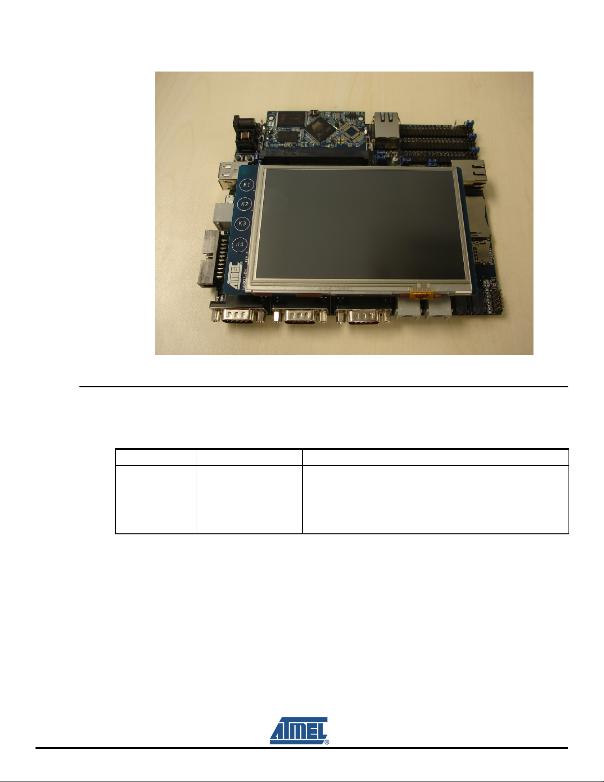
Figure 1-1. Board Photo (Display module is optional)
1.2 Applicable Documents
Table 1-1. Applicable Documents
Reference Title Comment
Atmel lit° 11052
Atmel lit° 11032
Atmel lit° 11054
Atmel lit° 11053
Atmel lit° 11055
http://www.atmel.com/products/at91/default.asp?category_id=163&family_id=605&source=global_nav
SAM9G15 datasheet
SAM9G25 datasheet
SAM9X25 datasheet
SAM9G35 datasheet
SAM9X35 datasheet
These documents provide technical support for each one of the
Atmel ARM-based Embedded MPU products supported by these
Evaluation Kits.
The datasheets can be found on www.atmel.com in the
SAM9G/SAM9X product families by means of the link below:
1-2 Evaluation Kit (EK) User Guide
11115A–ATARM–27-Jul-11
Page 7

2.1 Deliverables
The Evaluation Kits include:
Board
– One EK board
– One of the five available CPU modules (CM)
– One optional DM board featured in SAM9G15, SAM9G35, SAM9X35 kits only.
Power supply
– Universal input AC/DC power supply with US, Europe and UK plug adapters
– One 3V Lithium Battery type CR1225
Cables
– One serial RS232 cable
– One micro A/B-type USB cable
– One RJ45 crossed cable
A Welcome Letter
Section 2
Kit Contents
SAM9G15-CM
SAM9G35-CM
SAM9X35-CM
SAM9G25-CM
SAM9X25-CM
Evaluation Kit (EK) User Guide 2-1
11115A–ATARM–27-Jul-11
Page 8
Kit Contents
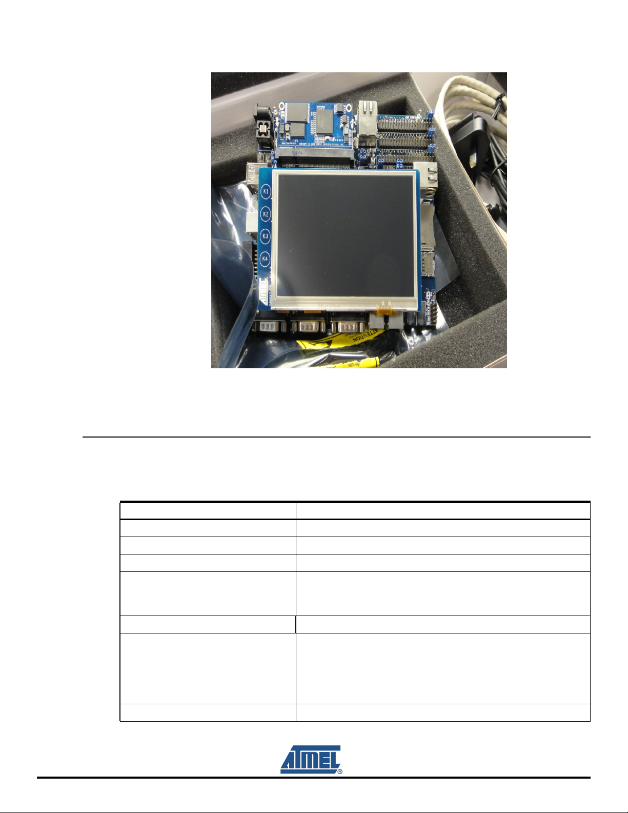
Figure 2-1. Unpacked Evaluation Kit
Unpack and inspect the kit carefully. Contact your local Atmel distributor, should there be issues concerning the contents of the kit.
2.2 Evaluation Board Specifications
Table 2-1. Evaluation Kit Specifications
Characteristics Specifications
Clock speed 400 MHz PCK, 133 MHz MCK
Ports Ethernet, USB, RS232, DBGU, JTAG, CAN, Audio, SD Card
Board supply voltage 5 VDC from connector
Temperature
- operating
- storage
Relative humidity 0 to 90% (non condensing)
Dimensions
EK (Evaluation Kit)
CM (Computer Module)
DM (Display Module)
-10° to +50° C
-40° to +85° C
165 mm x 135 mm
67.6 mm x 35 mm
135 mm x 80 mm
RoHS status Compliant
2-2 Evaluation Kit (EK) User Guide
11115A–ATARM–27-Jul-11
Page 9

2.3 Electrostatic Warning
The Evaluation Kit is shipped in a protective anti-static package. The board system must not be subjected to high electrostatic potentials. A grounding strap or similar ESD protective device should be worn
when handling the board in hostile ESD environments (offices with synthetic carpet, for example). Avoid
touching the component pins or any other metallic element on the board.
Kit Contents
Evaluation Kit (EK) User Guide 2-3
11115A–ATARM–27-Jul-11
Page 10

3.1 Power Up the Board
Unpack the board taking care to avoid electrostatic discharge. Unpack the power supply, select the right
power plug adapter corresponding to that of your country, and insert it in the power supply.
Connect the power supply DC connector to the board and plug the power supply to an AC power plug.
The board LCD should light up and display a welcome page. Then, click or touch icons displayed on the
screen and enjoy the demo.
3.2 DevStart
The on-board NAND Flash contains an installation guide named: “SAM9x5-EK DevStart”.
It is stored in the “SAM9x5-EK DevStart” folder on the USB Flash disk available when the Evaluation Kit
is connected to a host computer.
Click the file “welcome.html” in this folder to launch the SAM9x5-EK DevStart.
Section 3
Power Up
DevStart guides the user through the installation processes of IAR™ EWARM, Keil™ MDK and GNU
toolkits. Then, it gives step-by-step instructions on how to rebuild a single example project and how to
program it into the Evaluation Kit. Optionally, if the user has a SAM-ICE™ interface, instructions are also
given about how to debug the code.
It is strongly recommended that users backup the “SAM9x5-EK DevStart” folder on their computer before launching it.
Evaluation Kit (EK) User Guide 3-1
11115A–ATARM–27-Jul-11
Page 11
Power Up
3.3 Recovery Procedure
The DevStart ends by giving step-by-step instructions on how to recover the Evaluation Kit to the state
as it was when shipped by Atmel.
Follow the instructions if contents of the NAND Flash or the SPI DataFlash®have been deleted, in order
to recover from this situation.
3.4 Sample Code and Technical Support
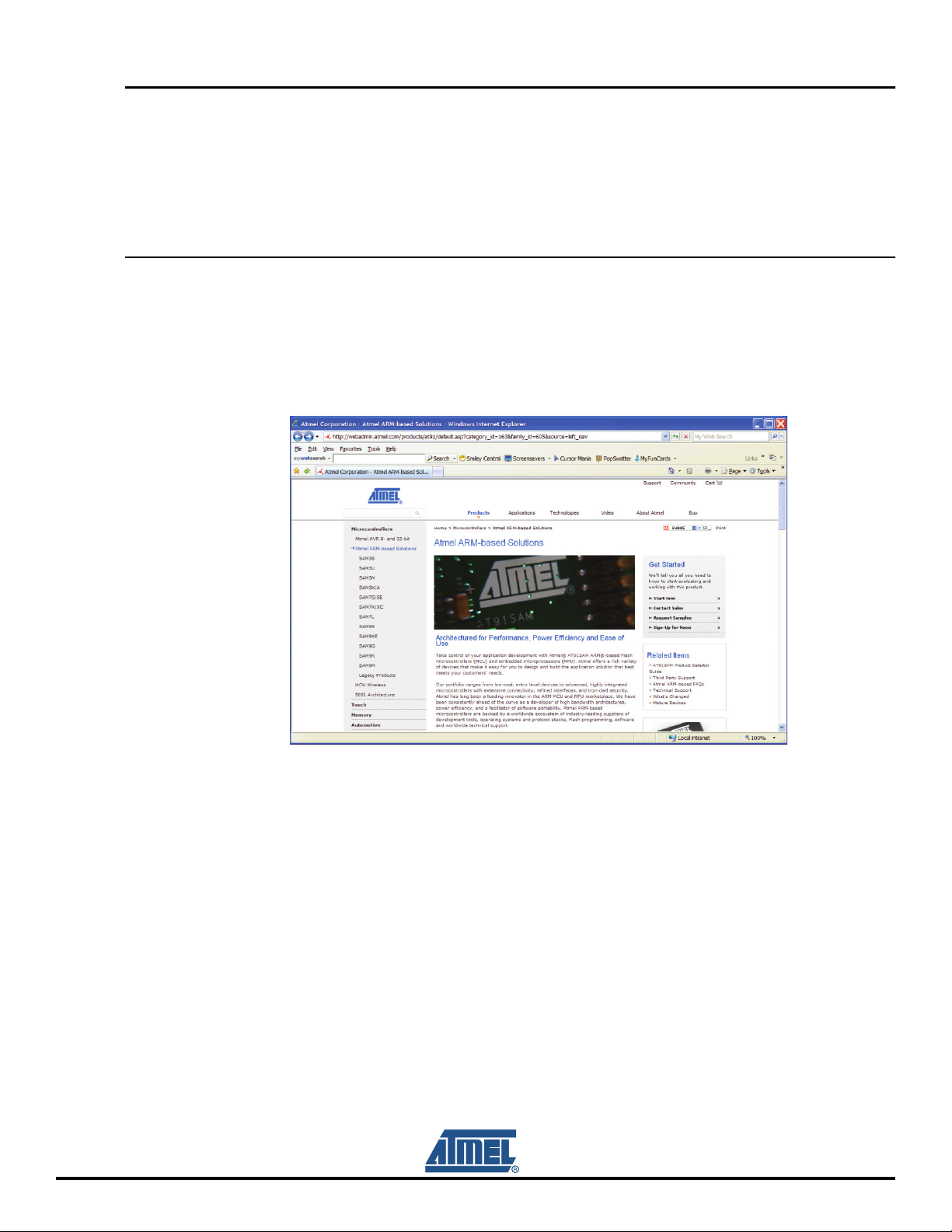
After boot up, designers can run sample code or their own application, on the development kit. Users
can download sample code and get technical support from the Atmel web site:
http://www.atmel.com/products/at91/default.asp?category_id=163&family_id=605&source=global_nav
Figure 3-1. Atmel Web Site
Note: Different interfaces on the EK boards share the same connections to the CPU module. Therefore the actual
usage depends on the CPU module featured in the evaluation kit.
3-2 Evaluation Kit (EK) User Guide
11115A–ATARM–27-Jul-11
Page 12

4.1 Introduction
The Evaluation Kit is a fully-featured evaluation platform for the Atmel MPU. The Evaluation Kit enables
users to extensively evaluate, prototype and create application-specific designs.
The Evaluation Kit is a new platform architecture based on a Main Board (MB), a CPU Module (CM)
equipped with one of the five processors and an optional Display Module (DM).
The Evaluation Kit consists of three boards:
1. The CPU Module (CM) board, is a single-board computer that integrates all the core components
and is mounted onto an application-specific carrier board (EK board). The CPU Module has specified pinouts based on the SODIMM200 connector. It provides the functional requirements for an
embedded application. These functions include, but are not limited to, graphics, audio, mass storage,
network and multiple serial and USB ports. A single SODIMM200 connector provides an interface for
the carrier board to carry all the I/O signals to and from the CPU Module.
2. The Evaluation Kit board (EK Main Board) provides all the interface connectors required to attach
the system to the application specific peripherals. This versatility allows the designer to create a
densely packed solution, which results in a more reliable product while simplifying system
integration.
3. The optional Display Module (DM) board integrates LCD, TouchScreen and Qtouch®technology.
Section 4
Evaluation Kit Hardware
Table 4-1, on the page that follows, lists the features provided on the Evaluation Kit:
Evaluation Kit (EK) User Guide 4-1
11115A–ATARM–27-Jul-11
Page 13
Evaluation Kit Hardware
Table 4-1. Evaluation Kit Features
Supported modules SAM9 products
Expansion Slot SO-DIMM200
Processor options
LAN
USART/UART
CAN CAN interface Shared interface
USB
SMD Software Modem Device X X X X X
Memory Card Support
MII/RMII Ethernet 10/100 w/PHY and three
Led status
RMII Ethernet 10/100 w/PHY and three Led
status
RS232 four wires/RS485
Shared interface
SAM9
G15
ETH0 X X X X
ETH1 X
COM0 X X X X X
SAM9
G25
SAM9
G35
SAM9
X25
SAM9
X35
RS232 four wires COM3 X X
RS232 two wires DBGU X X X X X
CAN0 X X
CAN1 X X
2 * USB 2.0 Host X X X X X
1 * USB 2.0 Host/Device X X X X X
µSD Card Slot Onboard
MMC/MMC+/SD/SDIO/CE-ATA
HSMCI
0
HSMCI
1
XXXXX
XXXXX
ISI X
LCD + Touch Screen 24-bit Output Mode X X X
ZigBee
®
XXXXX
SPI XXXXX
TWI XXXXX
DEBUG JTAG Test Access Port X X X X X
4-2 Evaluation Kit (EK) User Guide
11115A–ATARM–27-Jul-11
Page 14
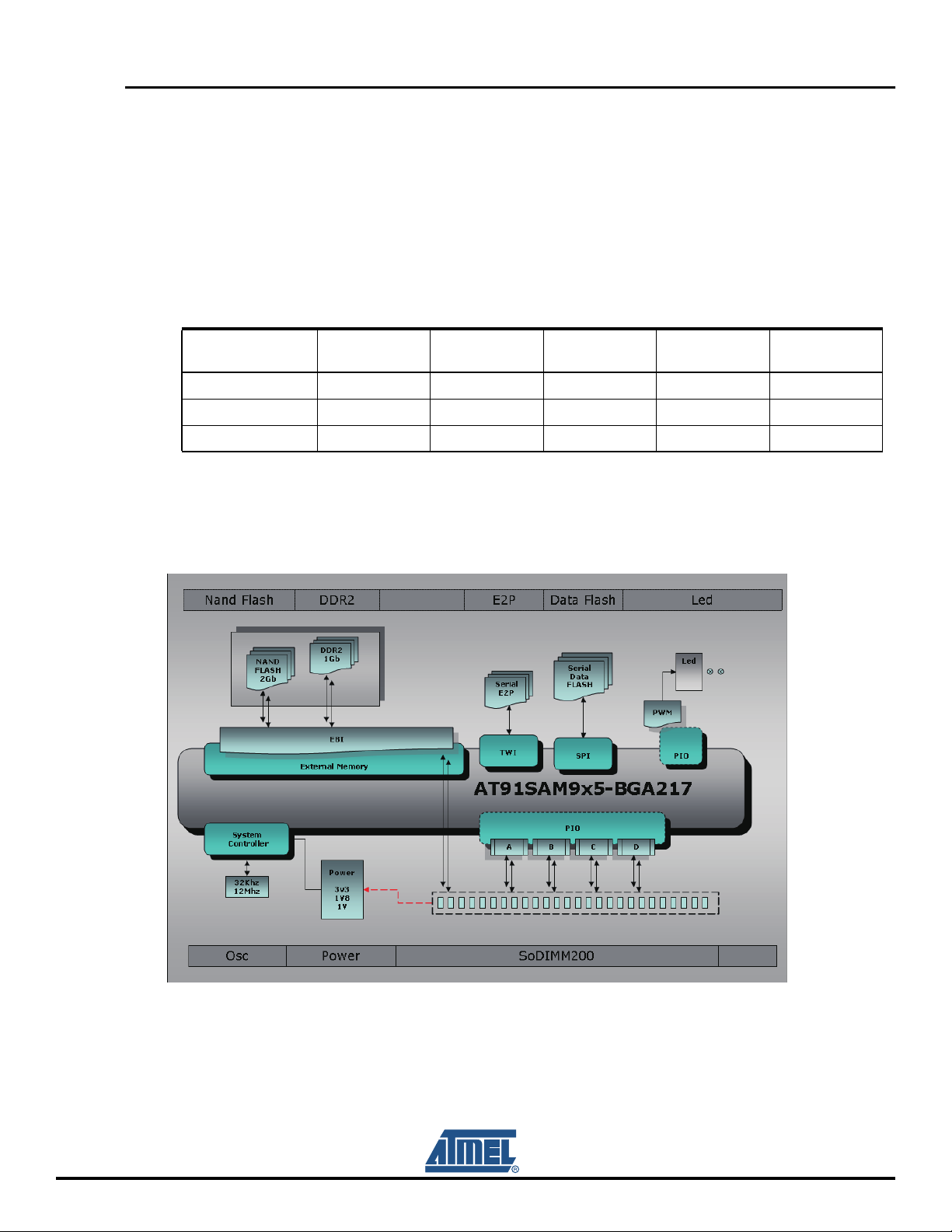
4.2 Computer Module (CM)
4.2.1 CM Board Overview
The CM board is the CPU module at the heart of the system. It connects to the EK board through a SODIMM200 interface. It carries the processor and external memories. The CM board serves as a minimal
CPU sub-system. All five processors:SAM9G15, SAM9G25, SAM9X25,SAM9G35 and SAM9X35 share
the same CM circuitry with minor configuration settings.
Note: There are three CM boards from three different manufacturers. The five processors are
implemented as shown in Table 4-2 below:
Table 4-2. CM Board Implementation
Evaluation Kit Hardware
Manufacturer &
Module kind
mfg 1 x x
mfg 2 x x
mfg3xxxxx
The three CM boards share the same circuitry design but with different designator information and PCB layouts. The
circuitry reference in this guide, for common design parts, refers to schematics from SAM9G25-CM (mfg 3). All the
other schematics are provided in
Figure 4-1. Board Architecture
SAM9G15-CM SAM9G25-CM SAM9G35-CM SAM9X25-CM SAM9X35-CM
Section 4.2.6 ”Schematics”.
4.2.2 Equipment List
The CM board is built around the integration of an ARM926-based microcontroller (BGA217 package)
with external memory and optional Ethernet PHYsical Layer Transceiver.
Evaluation Kit (EK) User Guide 4-3
11115A–ATARM–27-Jul-11
Page 15
Evaluation Kit Hardware
4.2.2.1 Devices
Following is the list of the CM board components:
One SAM9 Embedded MPU from the list below
– SAM9G15
– SAM9G25
– SAM9G35
– SAM9X25
– SAM9X35
12 MHz crystal
32.768 KHz crystal
1 Gbit DDR2 memory
2 Gits NAND Flash memory with Chip Selection control switch
32 Mbits SPI Serial DataFlash with Chip Selection control switch
512 Kbits EEPROM
1 Kbyte 1-Wire EEPROM
On-board power regulation
Two user LEDs
Optional PHY
4.2.2.2 Interface Connection
SODIMM200 card edge interface
4.2.2.3 Configuration Items
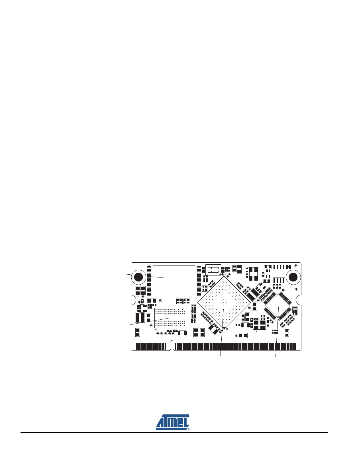
Dual ON/OFF switch for NAND Flash and SPI DataFlash Chip Select connection
Figure 4-2. CM Board Layout Commented
DDR2 SDRAM
NAND Flash
Sodimm200 card edge
SAM9 chip
PHY
4-4 Evaluation Kit (EK) User Guide
11115A–ATARM–27-Jul-11
Page 16
4.2.3 Function Blocks
4.2.3.1 Processor
The CM Board is equipped with an Atmel ARM-based embedded MPU, as listed below, in a 217-ball
BGA package. The five devices share an identical footprint. All five share the same CM Board PCB with
minor configuration differences.
The five devices are:
SAM9G15
SAM9G25
SAM9G35
SAM9X25
SAM9X35
As different interfaces can be defined using the same pins, it depends on the actual configuration of the
CPU as to which functions are in fact available to the EK board.
Refer to Section 4.2.4.1 ”Chip Identification” for details. The processor runs at a nominal frequency of
400 MHz for the core and 133 MHz for the system bus.
The peripheral configuration possibilities and implementation requirements of the CM are dependent on
the module's chipset. Two configuration resistors are implemented on board in order to select the mode
of configuration.
Evaluation Kit Hardware
4.2.3.2 Clock Circuitry
The CM includes 3 clock sources:
Two are alternatives for the processor main clock
One crystal and one crystal oscillator are used for the Ethernet MII/RMII chip
Table 4-3. Main Components Associated with the Clock Systems
Quantity Description Component assignment
4.2.3.3 Reset Circuitry
The reset sources for the CM board are:
Power on reset
Push button reset (Push button is equipped on EK board)
JTAG reset from an in-circuit emulator (JTAG interface is equipped on EK board)
1 Crystal for Internal Clock, 12 MHz Y1
1 Crystal for RTC Clock, 32.768 kHz Y2
1 Oscillator for Ethernet Clock RMII, 50 MHz Y3
Evaluation Kit (EK) User Guide 4-5
11115A–ATARM–27-Jul-11
Page 17

Evaluation Kit Hardware
4.2.3.4 Power Supplies
The CM Board is driven by +3V3 input power rail from the EK board through the SODIMM200 connector.
The CM Board embeds all the necessary power rails required for the micro processor.
When additional voltages are required, for example VDDCORE, they are generated on board from the
3.3V supply. The detailed power supply requirements for any given module are specified within the cor-
responding product documentation. The following table summarizes the power specifications.
Table 4-4. Power Rails Associated with the Systems
Nominal Name Powers Component
3.3v VDDNF
3.3v VDDIOP0 Partial Peripheral I/O lines From SODIMM200 connector
3.3v VDDIOP1 Partial Peripheral I/O lines From SODIMM200 connector
3.0v VDDBU
3.3v VDDUTMII the USB device and host UTMI+ interface From SODIMM200 connector
3.3v VDDOSC the Main Oscillator cells From SODIMM200 connector
3.3v VDDANA the Analog to Digital Converter From SODIMM200 connector
1.8v VDDIOM the External Memory Interface I/O lines on-board
1.0v VDDUTMIC DC Supply UDPHS and UHPHS UTMI+ Core on-board
3.3v VDDPLLUTMI
1.0v VDDPLLA the PLLA cell on-board
1.0v VDDCORE
3.0V or 3.3V
configurable
ADVREF ADC Reference voltage From SODIMM200 connector
the NAND Flash I/O and control, D16-D32 and
multiplexed SMC lines
the Slow Clock oscillator, the internal 32 kHz
RC, the internal 12 MHz RC and a part of the
System Controller
DC Supply UDPHS and UHPHS UTMI+
Interface
the core, including the processor, the
embedded memories and the peripherals
From SODIMM200 connector
From SODIMM200 connector
From SODIMM200 connector
on-board
4-6 Evaluation Kit (EK) User Guide
11115A–ATARM–27-Jul-11
Page 18
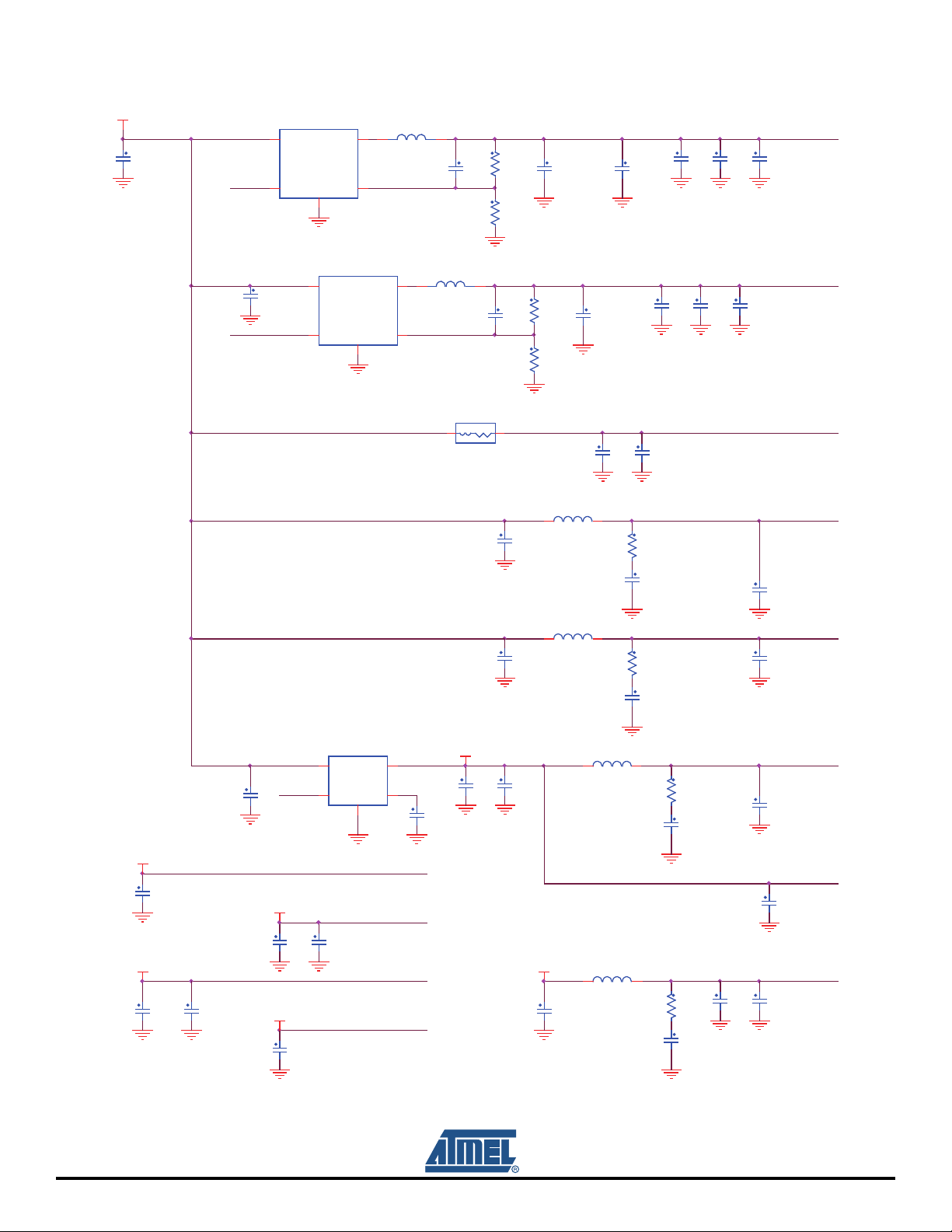
Figure 4-3. CM Power Supply
+3V3 MN3
4
C10
4.7uF
1
PWR_EN
AS1301EHT-adj
IN
GND
EN
2
LX
FB
3
2.2uH 3D 16
5
Evaluation Kit Hardware
L2
C7
C11
22pF
R2
39.2K 1%
R4
59K 1%
C12
10uF
C3
4.7uF
C6
100nF
100nF
C8
100nF
VDDCORE
PWR_EN
C1
4.7uF
MN1
AS1301EHT-adj
4
IN
1
EN
L1
3
LX
2.2uH 3D 16
R1
C9
118K 1%
5
GND
FB
2
120 OHM@100MHZ
22pF
R3
59K 1%
B2
21
C38
100nF
C41
100nF
C2
10uF
L5
10uH/150m A
L6
10uH/150m A
C39
4.7uF
C43
4.7uF
C4
100nF
R22
1R
R25
1R
C5
100nF
C13
100nF
C14
100nF
C15
100nF
C40
100nF
C42
100nF
VDDIOM
VDDNF
VDDUTMII
VDDOSC
C27
100nF
L4
10uH/150m A
L3
10uH/150m A
C34
4.7uF
C28
4.7uF
R17
1R
R10
1R
C25
100nF
C33
100nF
C30
100nF
C26
100nF
VDDPLLA
VDDUTMIC
VDDAN A
ADVREF
C35
100nF
VDDI OP0
C20
100nF
C21
100nF
C17
1uF
VDDBU
VDDIOP1
PWR_EN
C36
1uF
C23
100nF
MN4
TPS71710DCK
IN1OUT
GND
EN3NR
2
C37
100nF
5
4
ADVREF
VDDBU
VDDI OP0
VDDI OP1
C18
10nF
+1V
C16
1uF
C32
100nF
VDDANA
Evaluation Kit (EK) User Guide 4-7
11115A–ATARM–27-Jul-11
Page 19

Evaluation Kit Hardware
4.2.3.5 Memory
The Device serial processor features a DDR/SDR memory interface and an External Bus Interface (EBI)
to enable interfacing to a wide range of external memories and to almost any kind of parallel peripheral.
The External Bus Interface (EBI) is connected to two kinds of memory devices:
One 1 Gbyte DDR2 SDRAM
One 2 Gbytes (or 4 Gbytes depending on supplier) NAND Flash
4-8 Evaluation Kit (EK) User Guide
11115A–ATARM–27-Jul-11
Page 20
Figure 4-4. CM Board External Memory
C50 100nF
C52 100nF
C48 100nF
C49 100nF
J1
VDD
VDDL
CKEK2CKJ8CK
K8
DDR2_SDCK
DDR2_NSDCK
A9
C1
VDDQ
C51 100nF
VDDQC3VDDQC7VDDQ
VDDQ
CS
L8
DDR2_NCS1
DDR2_D9
DDR 2_D12
DDR 2_D11
DDR 2_D10
DDR 2_D14
DDR2_D2
DDR2_D1
DDR2_D0
DDR2_D3
DDR2_D4
DDR2_D5
DDR2_D6
DDR2_D7
F9
DQ0G8DQ1G2DQ2H7DQ3H3DQ4H1DQ5H9DQ6F1DQ7
DDR2 SDRAM
MT47H64M16HR
A0M8A1M3A2M7A3N2A4N8A5N3A6N7A7P2A8P8A9P3A10M2BA0L2ODT
MN5
EBI_A3
EBI_A4
EBI_A5
EBI_A6
EBI_A7
EBI_A8
EBI_A2
EBI_A9
DDR2_D8
EBI_A10
C2
DQ8C8DQ9
EBI_A11
DDR 2_D13
DQ10D7DQ11D3DQ12D1DQ13D9DQ14B1DQ15
A11P7BA1
A12R2BA2
EBI_SDA10
EBI_A13
EBI_A14
EBI_A16
B9
L3
DDR 2_D15
EBI_A17
L1
EBI_A18
VDDI OM
C44 100nF
C47 100nF
C45 100nF
C46 100nF
M9
E1
A1
R1
VDDJ9VDD
VDD
VDD
K9
DDR2_SDCKE
C53 100nF
C9
C54 100nF
C56 100nF
C55 100nF
E9
VDDQ
VDDQG1VDDQG7VDDQ
CASL7RASK7WE
DDR2_RAS
DDR2_CAS
G3
C57 100nF
VDDQ
K3
DDR2_SDWE
C58 100nF
G9
C59 100nF
Evaluation Kit Hardware
C66
100nF
C60
100nF
C65
12
37
VCC
VCC
N.C811N.C710N.C914N.C10
100nF
34
39
36
13
25
48
VSS
VSS
VSS_N.C
N.C1223N.C13
VSS_N.C
DNU121DNU2
N.C14
DNU3
MT29F2G08AAD
22
24
35
38
NANDCS
NANDCLE
NANDALE
NANDWE
NANDOE
NANDR_B
VCC_N .C
VCC_N .C
N.C11
20
15
DDR2 SDRAM
DDR_VREF
J2
E3
VSSA3VSS
VREF
UDQSB7UDQS
A8
DDR2_DQS1
B2
J3
N1
P9
VSS
VSS
VSS
VSSQA7VSSQB8VSSQH2VSSQ
UDM
LDQSE8LDQS
F3
B3
F7
DDR2_DQM1
DDR2_DQM0
DDR2_DQS0
VSSQ
LDM
D2
VSSQD8VSSQE7VSSQF2VSSQ
VSSQ
F8
RFU1A2RFU2
RFU3
E2
R3
H8
J7
VSSDL
RFU4R7RFU5
R8
EBI_A15
NAND_FSH_D2
NAND_FSH_D6
NAND_FSH_D3
NAND_FSH_D4
NAND_FSH_D5
NAND_FSH_D1
NAND_FSH_D0
29
I/O0
I/O130I/O332I/O2
MN1 1
ALE
CLE
17
16
CLE
ALE
R40 0R
R43 0R
PD3
PD2
NAND_FSH_D7
31
41
I/O744I/O643I/O542I/O4
WE
CE9RE
R/B
8
7
18
19
WP
CEWERE
RB
R47 470K
R42 0R
R44 0R
R41 0R
R46 470K
R48 470K
PD0
PD1
PD5
NAND FLASH
28
33
45
40
27
I/O8_N.C26I/O9_N.C
I/O10_N .C
I/O11_N .C
I/O12_N .C
WP
N.C11N.C22N.C33N.C4
5
4
R49
DNP
I/O15_N .C47I/O14_N .C46I/O13_N .C
N.C5
6
VDDNF
N.C6
DDR2_D1
DDR2_D0
DDR2_D5
DDR2_D4
DDR2_D3
DDR2_D2
DDR2_D6
RR1B
RR1A
RR2C
RR1D
RR2A
RR1C
2 7
EBI_D0
SAM9x5_LBGA217 - EBI
MN2 F
RR2B
1 8
3 6
4 5
1 8
3 6
2 7
EBI_D1
EBI_D3
EBI_D2
EBI_D5
EBI_D4
EBI_D6
EBI_D2
EBI_D3
EBI_D4
EBI_D5
EBI_D0
EBI_D1
D14D1D15D2A16D3B16D4A17D5B15D6C14D7B14D8A15D9C15
D0
VDDNF
VDDNF
R34
1.5K 1%
DDR2_D9
DDR2_D8
DDR2_D7
RR2D
4 5
EBI_D7
EBI_D6
DDR2_D13
DDR2_D12
DDR2_D11
DDR2_D10
DDR2_D15
DDR2_D14
EBI_A11
F15
DDR2_SDCK
R36 27R
EBI_SDC K
D17
A11
A12
DDR2_NSDCK
R37 27R
EBI_NSDCK
EBI_A13
C17
EBI_A14
E16
A13
A14
EBI_A15
D16
A15
DDR2_NCS1
R38 27R
EBI_NCS1_SDCS
EBI_A16
C16
A16/BA0
EBI_A17
B17
EBI_A18
E15
A17/BA1
A18/BA2
E14
A19
EBI_DQM0
A10
C62
104
R33
1R
L7
10uH
150mA
C61
4.7uF
VDDIOM
EBI_DQS0
EBI_DQM1
EBI_DQS1
EBI_RAS
EBI_SDW E
EBI_CAS
A9
A11
B10
B11
C10
A12
RAS
CAS
DQS1
DQS0
DQM1
DQM0
DDR2_DQS1
EBI_A4
R29 27R
EBI_DQS1
EBI_A5
EBI_A6
DDR2_RAS
R30 27R
EBI_RAS
DDR2_CAS
R31 27R
EBI_CAS
EBI_A7
EBI_A8
DDR2_SDWE
R32 27R
EBI_SDW E
EBI_A9
R35 27R
EBI_SDC KE
EBI_A10
G14
A10
DDR2_DQM1
DDR2_DQM0
DDR2_DQS0
RR3A
RR3D
RR4B
4 5
2 7
EBI_D9
EBI_D8
EBI_D7
EBI_D8
RR4C
RR4A
RR3B
RR3C
RR4D
1 8
3 6
1 8
2 7
3 6
4 5
EBI_D13
EBI_D12
EBI_D11
EBI_D10
EBI_D15
EBI_D14
EBI_D9
EBI_D11
EBI_D10
EBI_D14
EBI_D12
EBI_D13
D12
C13
A14
B13
A13
D10
D11
D12
D13
D14
R26 27R
EBI_DQM0
EBI_D15
C12
J15
H16
D15
A0/NBS0
R28 27R
R27 27R
EBI_DQM1
EBI_DQS0
EBI_A2
EBI_A3
H15A3H17A4G17A5G16A6F17A7E17A8F16A9G15
A2
A1/NBS2/ DQM2/NWR2
DDR2_SDCKE
SDWE
EBI_SDC KE
B12
R39
1.5K 1%
ON
C64
104
1
SW1A
SWITCH -2-1.27mm
C63
4.7uF
NCS0
EBI_SDC K
EBI_NSD CK
EBI_SDA10
EBI_NCS1_SDCS
A8
C11
C8
D11
SDCK
SDA10
SDCKE
C7
D9
C9
B9
B8
NWR 1/NBS1
NWR0/NWRE
NRD
NWR 3/NBS3/DQM3
NCS0
#SDCK
NCS1/ SDCS
1 4
PD4
(NAND OE)
PD0
P13
SAM9x5_LBGA217 - PIOD
MN2 E
NAND_FSH_D1
NAND_FSH_D0
NAND_FSH_D3
NAND_FSH_D2
NAND_FSH_D6
NAND_FSH_D5
NAND_FSH_D4
NAND_FSH_D7
RR16A
RR16B
RR16C
RR17A
RR17B
1 8
2 7
PD7
PD6
PD[5..21] {3,5}
(NAND CS)
(NAND CLE)
(NAND WE)
(NAND ALE)
PD5
PD4
PD6
PD1
PD3
PD2
N14
P14
R14
P15
R13
P12
PD6/D 16
PD4/N CS3
PD5/N WAIT
PD0/N ANDOE
PD1/N ANDWE
PD2/A21/ NANDALE
PD3/A22/ NANDCLE
RR16D
RR17C
RR17D
1 8
2 7
3 6
3 6
4 5
PD9
PD8
PD12
PD11
PD10
PD7
PD9
PD8
PD10
PD11
R15
M14
N16
N17
N15
PD7/D 17
PD8/D 18
PD9/D 19
PD10/D 20
PD11/D 21
4 5
PD13
PD12
K15
R50 0R
R51 0R
R55 0R
R52 0R
R53 0R
R54 0R
(NANDCS)
(NANDCLE)
(NANDWE)
(NAND OE)
(NANDALE)
(NANDR/B)
PD6
PD3
PD4
PD1
PD0
PD2
PD13
PD15
PD14
PD19
PD18
PD17
PD16
PD20
PD21
M16
L16
L15
K17
J17
K16
PD16/D 26/A23
PD17/D 27/A24
PD18/D 28/A25
J16
PD19/D 29/NCS2
PD20/D 30/NCS4
PD21/D 31/NCS5
M15
L14
PD12/D 22
PD13/D 23
PD14/D 24
PD15/D 25/A20
Evaluation Kit (EK) User Guide 4-9
11115A–ATARM–27-Jul-11
Page 21
Evaluation Kit Hardware
4.2.3.6 Serial Peripheral Interface (SPI) Controller
The serial processor provides two high-speed Serial Peripheral Interface (SPI) controllers. One port is
used to interface with the on-board serial DataFlash
Figure 4-5. SPI
PA14
4.2.3.7 Two Wire Interface (TWI)
The serial processor has a full speed (400 kHz) master/slave TWI Serial Controller. The controller is
mostly compatible with industry standard I2C and SMBus Interfaces. This port is used to interface with
the on-board Serial EEPROM, ISI, QTouch device and audio codec interface.
Figure 4-6. TWI
SW1B
SWITCH -2-1.27mm
2 3
ON
2
PA12
PA11
PA13
(SPI0_MOSI)
(SPI0_MIS0)
(SPI0_SPCK)
(SPI0_NPC S0)
VDDI OP0
®
.
VDDI OP0
R56
470K
MN7
AT25DF321
R57 0R
R58 0R
R59 0R
VDDI OP0 VDDIOP0
5
2
6
1
SI
SO
SCK
CS
VCC
WP
HOLD
GND
VDDIOP0
8
3
7
4
C69
100nF
4.2.3.8 1-Wire EEPROM
The Evaluation Kit uses a 1-Wire device as “firmware label” to store the information such as chip type,
manufacturer’s name, production date etc.
Figure 4-7. 1-Wire Device
PA31
PA30
PB18
(TWCKO)
(TWDO)
R61
4.7K
VDDI OP0 R64
R66 0R
C70
100nF
R62
4.7K
VDDAN A
6
5
8
4
MN8
AT24C512BN-SH25-B
MN9
DS2431P+
2
IO
WP
A0
A1
A3
R65
1.5K
SCL
SDA
VCC
GND
1
2
3
7
NC1
NC2
NC3
GND
NC4
1
R63
10K
DNP
3
4
5
6
4-10 Evaluation Kit (EK) User Guide
11115A–ATARM–27-Jul-11
Page 22

4.2.3.9 Optional PHY
Some of the device modules provide a location for a 10/100 Ethernet MAC/PHY interface.
For more information about the Ethernet controller device, refer to the Davicom DM9161 controller manufacturer's datasheet.
Evaluation Kit Hardware
Evaluation Kit (EK) User Guide 4-11
11115A–ATARM–27-Jul-11
Page 23
Evaluation Kit Hardware
Figure 4-8. Ethernet
PB[0.. 18]
PB6
PB5
PB8
E0_MDIO
E0_MDC
E0_INTR
1 8
1 8
2 7
RR15A
RR14A
RR14B
VDDAN A
NRST
R99 0R
10KX4
10KX4
RR7
RR8
1
2
3
4 5
1
2
3
4 5
R91 DNP
R92 4.7K
R93 10K
R94 10K
R95 DNP
C80 100nF
C81 100nF
8
7
6
8
7
6
VDDAN A
R86 1.5K
PB3
PB1
PB0
PB2
E0_RX0
E0_RX1
E0_RXDV
E0_RXER
4 5
2 7
3 6
RR15C
3 6
RR14D
RR15B
RR14C
TP27
SMD
PB4
PB10
PB9
PB7
E0_TX0
E0_TX1
E0_TXEN
E0_TXCK
R73 22R
2 7
4 5
3 6
RR13B
RR13D
RR13C
R74 22R
DNP to remain
single PHY
connection on
EK board
VSS OUT
32
100nF
Y3
OE
50MHz
R70
10K
VDD
41
VDDAN A
C71
VDDAN A
40
15
33
VDDANA
+
C82
10uF
R100
0R
GND_ETH
RESET
N.C
45
PWRD WN10DGND
CABLESTS/LIN KSTS
DGND44DGND
LED2/OP213LED1/OP112LED0/OP0
14
LEDMODE
BGRES
31
11
1
2
3
4 5
23
DVDD
DVDD30DVDD
BGRESG
48
R97
6.8K
R98
10K
8
7
6
RR9
10KX4
41
47
R96 0RC79 100nF
GND_ETH
GND_ETH
32
24
DM9161AEP
AVDDT
C74 100nF
+
C75
10uF
+
C76
10uF
49.9R 1%
49.9R 1%
38
TX_ER/TXD416COL/R MII36MDC
CRS/ PHYAD435MDI O25MDI NTR
2
RX_CLK/10BTSER34RX_DV/TESTMODE37RX_ER/RXD4/RPTR
AVDDR1AVDDR
RX-
4
C73 100nF
BLM21BD222TN1
AVDDTB1
TP28
SMD
R83
R84
39
DISMDIX
AVDDT
AGND5AGND
AGND
9
6
46
C77 100nF
VDDAN A
C78
100nF
RXD0/PHYAD029RXD1/PHYAD128RXD2/PHYAD227RXD3/PHYAD3
RX+
3
22
26
TX_EN
TX-
8
21
TXD317TXD218TXD020TXD119TX_CLK/I SOLATE
TX+7XT1
42
MN1 0
REF_CLK/XT2
43
49.9R 1%
R71
C72 100nF
R72
49.9R 1%
GND_ETH
ETH0_RX+
LED0
LED1
LED2
ETH0_RX-
ETH0_TX+
ETH0_TX-
4-12 Evaluation Kit (EK) User Guide
11115A–ATARM–27-Jul-11
Page 24
4.2.3.10 SODIMM200 Interface
The CM board uses SODIMM200 card edge connector to interface with the EK board.
Figure 4-9. SODIMM200 Interface on CM Board
+3V3
C83
VDDI OP0
VDDI OP1
HHSD PC
HHSDMC
HHSDMB
HHSD PB
DIBP
DIBN
HHSDMA
HHSD PA
NANDOE
NAND ALE
NANDCS
NANDR_B
ETH0_TX+
ETH0_TXETH0_RX+
ETH0_RX-
PD8
PD10
PD12
PD14
PD16
PD18
PD20
PA0
PA2
PA4
PA11
PA13
PA8
PA22
PA31
PA16
PA18
PA20
PA5
PA10
PA25
PA27
PA29
PC0
PC2
PC4
PC7
PC9
PC11
PC12
PC14
PC17
PC19
PC21
PC22
PC24
PC26
PC29
PC31
PB0
PB2
PB4
PB6
PB8
PB9
PB11
PB13
PB15
PB17
PB18
10uF
VDDNF
VDDANA
J1
VCC_3V31VCC_3V3
VCC_3V33VCC_3V3
5
GND
USBC_D P7JTAGSEL
USBC_D M9WKUP
11
GND
13
USBB_DM
15
USBB_DP
17
GND
19
DIBP
21
DIBN
23
GND
25
USBA_DM
27
USBA_DP
29
GND
31
RFU1
33
RFU3
35
RFU5
37
RFU7
39
RFU9
41
GND
43
RFU11
45
RFU13
47
RFU15
49
RFU17
51
GND
53
RFU19
55
RFU21
57
RFU23
59
RFU25
61
VDDNF
63
PD0
65
PD2
67
PD4
69
PD6
71
PD8
73
NC
75
PD10
77
PD12
79
PD14
81
PD16
83
PD18
85
PD20
VDDIOP087VDDIOP0
89
PA0
91
PA2
93
PA4
95
PA11
97
PA13
99
GND
101
PA8
103
PA22
105
PA31
107
GND
109
PA16
111
PA18
113
PA20
115
PA5
117
PA10
119
GND
121
PA25
123
PA27
125
PA29
127
VDDIOP1
129
PC0
131
PC2
133
PC4
135
GND
137
PC7
139
PC9
141
PC11
143
PC12
145
PC14
147
GND
149
PC17
151
PC19
153
PC21
155
PC22
157
PC24
159
PC26
161
GND
163
PC29
165
PC31
167
VDDANA
169
PB0
171
PB2
173
PB4
175
PB6
177
PB8
179
PB9
181
PB11
183
PB13
185
PB15
187
PB17
189
PB18
191
GND
193
ETH0_TX+
195
ETH0_TX-
197
ETH0_RX+
199
ETH0_RX-
PIO 200-pin SODI MM
VBAT
SHDN
BMS
nRST
nTRST
TCK
TMS
TDO
RTCK
PWR_EN
RFU2
RFU4
RFU6
RFU8
RFU10
GND
RFU12
RFU14
RFU16
RFU18
GND
RFU20
RFU22
RFU24
RFU26
VDDNF
PD1
PD3
PD5
PD7
PD9
GND
PD11
PD13
PD15
PD17
PD19
PD21
PA1
PA3
GND
PA12
PA14
PA7
PA21
PA23
PA30
PA15
PA17
PA19
GND
PA6
PA9
PA24
PA26
PA28
GND
VDDIOP1
PC1
PC3
PC5
PC6
PC8
PC10
GND
PC13
PC15
PC16
PC18
PC20
GND
PC23
PC25
PC27
PC28
PC30
SELCONFIG0
VDDANA
PB1
PB3
PB5
PB7
GNDANA
PB10
PB12
PB14
PB16
GNDANA
ADVREF
LED0
LED1
LED2
AVDDT
GND_ETH
Evaluation Kit Hardware
VDDBU
VDDNF
VDDANA
GND_ETH
C84
1uF
PD5
PD7
PD9
PD11
PD13
PD15
PD17
PD19
PD21
PA1
PA3
PA12
PA14
PA7
PA21
PA23
PA30
PA15
PA17
PA19
PA6
PA9
PA24
PA26
PA28
PC1
PC3
PC5
PC6
PC8
PC10
PC13
PC15
PC16
PC18
PC20
PC23
PC25
PC27
PC28
PC30
PB1
PB3
PB5
PB7
PB10
PB12
PB14
PB16
AVDDT
C85
4.7uF
JTAGSEL
WKUP
SHDN
BMS
NRST
NTRST
TDI
TCK
TMS
TDO
RTCK
PWR_EN
NANDWE
NANDCLE
VDDI OP0
VDDI OP1
ADVREF
LED0
LED1
LED2
C86
4.7uF
C87
4.7uF
+3V3
R101
DNP
R102
0R
C88
1uF
R101 only if G15, G35, X35
R102 only if G25, X25
+3V3
2
4
6
8
10
12
14
16
18
20
TDI
22
24
26
28
30
32
34
36
38
40
42
44
46
48
50
52
54
56
58
60
62
64
66
68
70
72
74
76
78
80
82
84
86
88
90
92
94
96
98
100
102
104
106
108
110
112
114
116
118
120
122
124
126
128
130
132
134
136
138
140
142
144
146
148
150
152
154
156
158
160
162
164
166
168
170
172
174
176
178
180
182
184
186
188
190
192
194
196
198
200
Evaluation Kit (EK) User Guide 4-13
11115A–ATARM–27-Jul-11
Page 25
Evaluation Kit Hardware
4.2.4 Configuration
4.2.4.1 Chip Identification
The CM board may be equipped with any of the five processors, all sharing an identical BGA217 footprint. There are two resistors on the CM board for the purpose of identifying which of the five is the one
actually mounted.
The tables below show in detail how the CM board, relative to different processors, determines the dedicated “SELCONFIG” logic.
Table 4-5. Resistor Identification
Resistor SAM9G15 SAM9G25 SAM9G35 SAM9X25 SAM9X35
R49 Populated Not Populated
R50 Not Populated Populated
R87 Populated Populated
R88 Not Populated Not Populated
R101 Populated Not Populated Populated Not Populated Populated
R102 Not Populated Populated Not Populated Populated Not Populated
Table 4-6. Module Configuration Identification
SAM9G15
module
R101 Populated Populated Populated Not Populated Not Populated
CM
Setting
EK
Setting
DM
Setting
R102 Not Populated Not Populated Not Populated Populated Populated
SELCONFIG
(SODIMM200
pin 166)
USART3 Not Selected Not Selected Not Selected Selected Selected
ETH1 Not Selected Not Selected Not Selected Not Selected Selected
LCD Selected Selected Selected Not Selected Not Selected
High High High Low Low
SAM9G35
module
SAM9X35
module
SAM9G25
module
SAM9X25
module
4-14 Evaluation Kit (EK) User Guide
11115A–ATARM–27-Jul-11
Page 26
4.2.4.2 Boot Configuration
In order to use SAM-BA boot, the NAND Flash and SPI DataFlash must be deselected. SW1 is dedicated to this purpose.
Table 4-7. Boot Configuration
4.2.5 Connectors
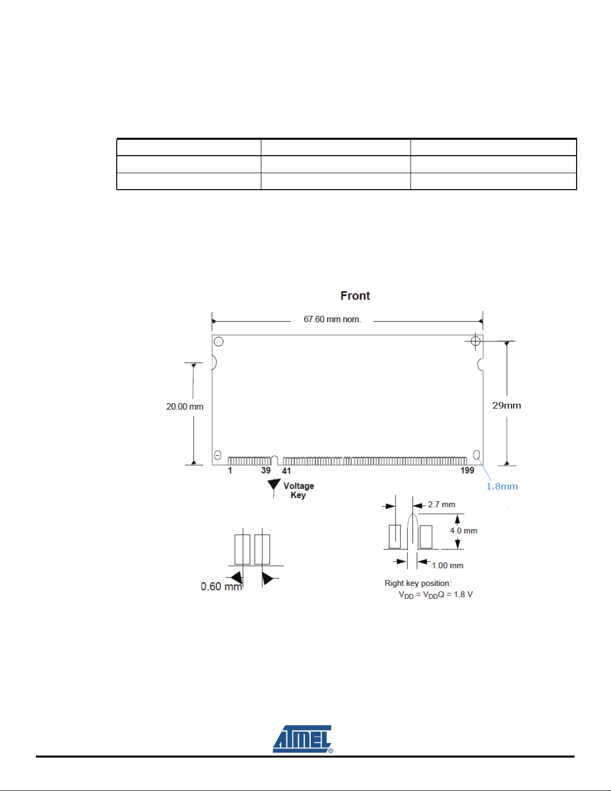
Figure 4-10. CM Board Dimensions
Evaluation Kit Hardware
Designation Default Setting Feature
SW1 (1, 4) ON Set to OFF disables the NAND flash
SW1 (2, 3) ON Set to OFF disables the SPI DataFlash
Evaluation Kit (EK) User Guide 4-15
11115A–ATARM–27-Jul-11
Page 27
Evaluation Kit Hardware
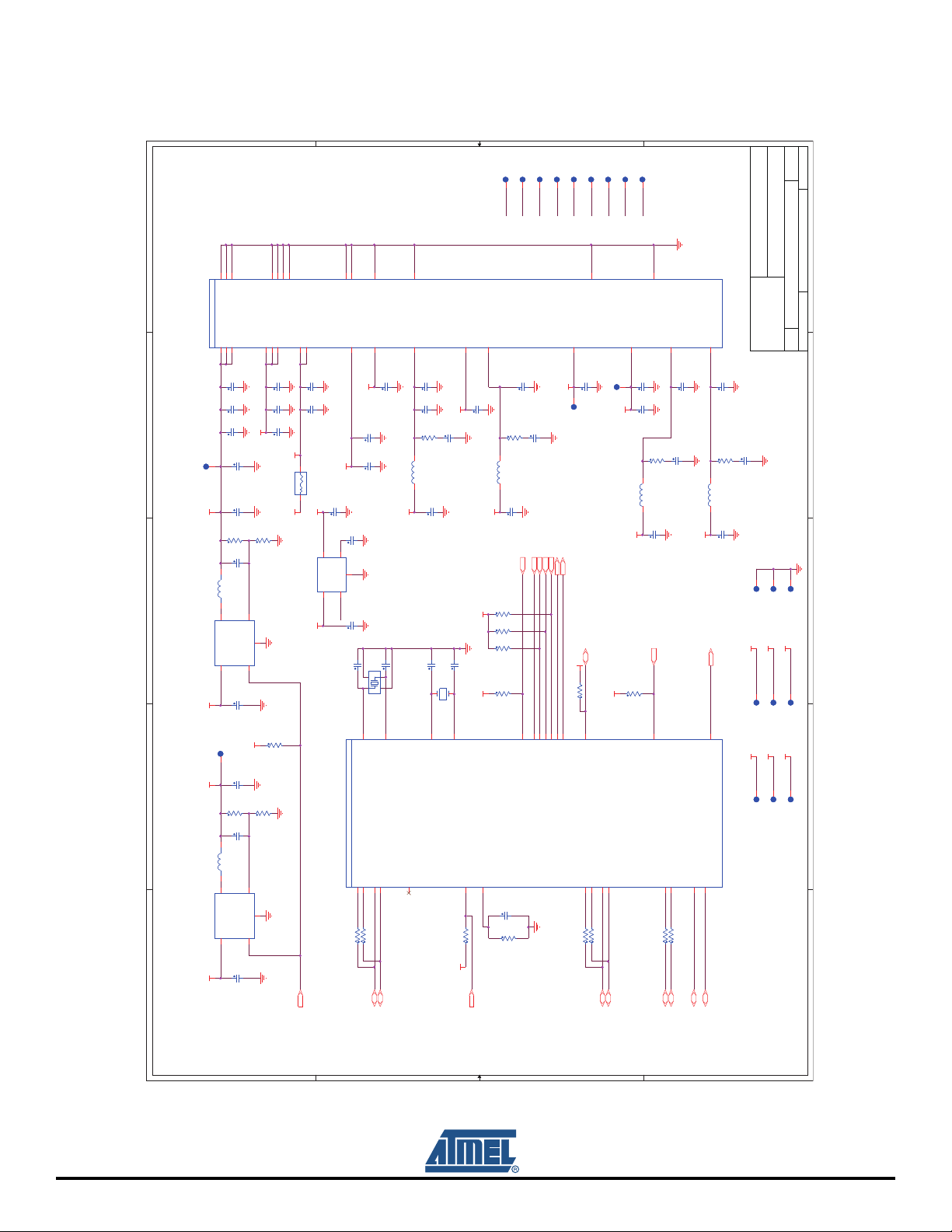
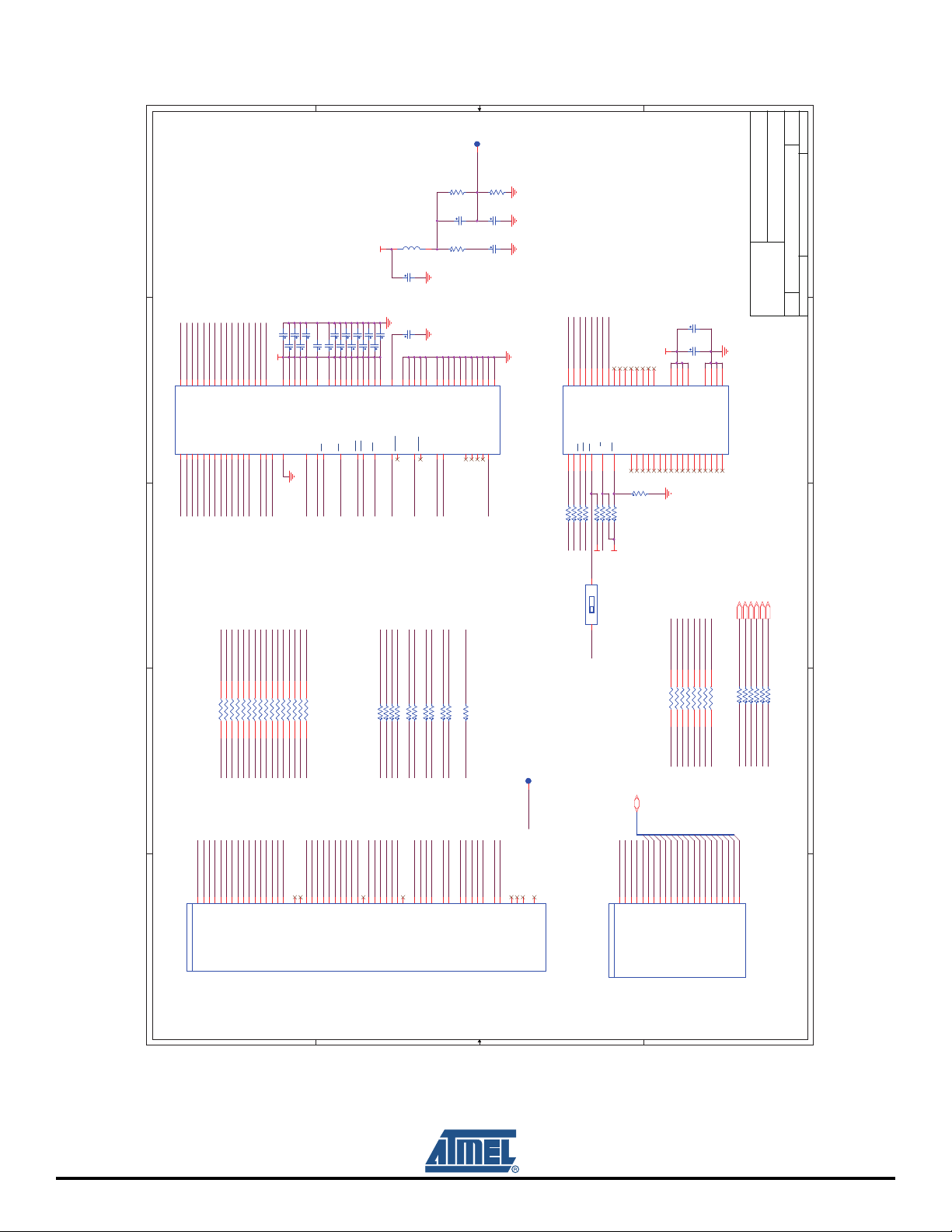
4.2.6 Schematics
Figure 4-11. CM Board Schematics – 1of 5
15Thursday,November 04,2010Zhu Xueliang
15Thursday,November 04,2010Zhu Xueliang
SMD
SMD
TP3
TP3
NTRST
SMD
SMD
SMD
SMD
TP4
TP4
TDI
SMD
SMD
SMD
SMD
TP5
TP5
TMS
SMD
SMD
TP6
TP6
TP8
TP8
TP9
TP9
TCK
RTCK
TDO
SMD
SMD
SMD
SMD
SMD
SMD
TP13
TP13
TP10
TP10
TP12
TP12
NRST
WKUP
SHDN
15Thursday,November 04,2010Zhu Xueliang
1
J10
H10
H9
K10
H8
GNDIOM
GNDIOMJ9GNDIOM
GNDIOM
GNDCOREJ8GNDCORE
GNDCORE
VDDIOM
VDDIOM
VDDIOM
VDDCOREK9VDDCOREK8VDDCORE
SAM9X5_LBGA217 - POWER
SAM9X5_LBGA217 - POWER
MN2A
MN2A
H14
C8
C7
2
3
C6
TP1
SMD
TP1
SMD
L2
2.2uH 3D16L22.2uH 3D16
3
LX
IN4EN
MN3
AS1301EHT-adj
MN3
AS1301EHT-adj
SMD
SMD
TP2
TP2
4
VDDIOM+3V3 VDDCORE+3V 3
100nFC8100nF
100nFC7100nF
100nFC6100nF
C3
C12
C12
R2
C11
C11
C10
C10
C2
R1
C9
F14
D13
D10
C15
C15
100nF
100nF
C14
C14
100nF
100nF
C13
C13
100nF
100nF
VDDIOM
4.7uFC34.7uF
10uF
10uF
39.2K 1%R239.2K 1%
22pF
22pF
VDDNF
B2
+3V3
R4
59K 1%R459K 1%
5
FB
GND
2
1
4.7uF
4.7uF
R6
DNPR6DNP
+3V3
10uFC210uF
118K 1%R1118K 1%
R3
59K 1%R359K 1%
22pFC922pF
M4
P6
GNDIOP
GNDIOP
VDDNF
VDDNF
J14
K14
21
VDDIOP 0P7VDDIOP 1
C5
100nFC5100nF
C4
100nFC4100nF
VDDIOP0
120 OHM@100MHZB2120 OHM@100MHZ
C16
C16
1uF
1uF
C18
C18
10nF
10nF
4
5
NR
OUT
GND
2
IN
EN
MN4
TPS71710DCK
MN4
TPS71710DCK
1
3
PWR_EN
C17
C17
1uF
1uF
+3V3 +1V
C19 20pFC19 20pF
1234
T12
XIN
T16
D6
GNDANA
GNDUTMI
C26
C26
100nF
100nF
C25
C25
100nF
100nF
R101RR10
10uH/150mAL310uH/150mA
C24
C24
1R
C27
C27
100nF
100nF
20pF
20pF
12
A6
XIN32
VDDUTMIC
VDDPLLA
T17
R12
C33
C33
100nF
100nF
C30
C30
100nF
100nF
+1V
R171RR17
1R
C34
C28
C28
4.7uF
4.7uF
L4
VDDIOP0
C29 20pFC29 20pF
VDDBU
Y2 32.768 kHzY2 32.768 kHz
A5
XOUT32
C34
4.7uF
4.7uF
10uH/150mAL410uH/150mA
C32
C32
100nF
100nF
+1V
NTRST {5}
TDI {5}
JTAGSEL {5}
R15
100K
R15
100K
R14
100K
R14
100K
R13
100K
R13
100K
R12
DNP
R12
DNP
NTRST
TDI
D7
T11
T9
TDI
NTRST
JTAGSEL
VDDANA
C6
H4
C23
C23
100nF
100nF
VDDIOP1
C21
C21
100nF
100nF
C20
C20
100nF
100nF
L3
VDDANA
Y1
12MHzY112MHz
C22 20pFC22 20pF
U12
XOUT
B6
GNDBU
ADVREF
A4
C35
C35
100nF
100nF
ADVREF
TP7
SMD
TP7
SMD
TDO {5}
RTCK {5}
TMS {5}
TCK {5}
NRST {4,5}
VDDIOP0
NRST
TMS
TCK
RTCK
TDO
R18 100KR18 100K
U10
U11
T10
R10
P10
TCK
TMS
TDO
RTCK
NRST
TP11
TP11
VDDBU
VDDBUB5VDDUTMII
SMD
SMD
VDDBU
L5
10uH/150mAL510uH/150mA
+3V3
R21
100K
R21
100K
U13
GNDOSC
VDDOSC
T13
U16
C40
C40
C37
C37
100nF
100nF
C36
C36
1uF
1uF
R221RR22
1R
C38
C38
100nF
100nF
WKUP {5}
WKUP
A7
WKUP
C42
C42
100nF
100nF
100nF
100nF
R251RR25
1R
C43
C39
C39
4.7uF
4.7uF
C43
4.7uF
4.7uF
L6
10uH/150mAL610uH/150mA
C41
C41
100nF
100nF
+3V3
TP16
SMD
TP16
SMD
SHDN {5}
VDDIOP0
SHDN
TP15
SMD
TP15
SMD
D8
SHDN
+3V3
TP14
SMD
TP14
SMD
1
MBC-SAM9X5
MBC-SAM9X5
MBC-SAM9X5
Title:
Title:
Title:
Date: Sheet: of
Date: Sheet: of
Date: Sheet: of
AT91SAM9G45-I&POWER A
AT91SAM9G45-I&POWER A
AT91SAM9G45-I&POWER A
A3
A3
A3
Size: Document Number: Rev:
Size: Document Number: Rev:
Draw By:
Draw By:
Draw By:
Size: Document Number: Rev:
2
TP19
SMD
TP19
SMD
TP22
SMD
TP22
SMD
3
VDDIOP1
VDDNF
TP18
SMD
TP18
SMD
TP21
SMD
TP21
SMD
+1V
VDDANA
4
TP17
SMD
TP17
SMD
TP20
SMD
TP20
SMD
L1
SAM9x5_LBGA217 - INTERFACE
2.2uH 3D16L12.2uH 3D16
3
5
LX
FB
GND
2
IN4EN
MN1
AS1301EHT-adj
MN1
AS1301EHT-adj
1
C1
5
4.7uFC14.7uF
D D
PWR_EN
PWR_EN{5 }
SAM9x5_LBGA217 - INTERFACE
HHSDMA
HHSDPA
HFSDMA
HFSDPA
MN2G
MN2G
T15
T14
U15
U14
R8 39RR8 39R
R7 39RR7 39R
HHSDMA{5}
HHSDPA{5 }
C C
M17
R23 27RR23 27R
HHSDMC{5}
HFSDPC
HFSDMC
L17
R24 27RR24 27R
HHSDPC{5}
DIBN
DIBP
P11
R11
5
DIBP{5}
DIBN{5}
A A
HHSDMB
HHSDPB
HFSDMB
TST
B7
BMSP9VBG
U17
C31
10pF
C31
10pF
R16
R16
6.8K
6.8K
R11 100KR11 100K
VDDIOP0
BMS{5}
HFSDPB
P17
P16
R17
R16
R19 39RR19 39R
R20 39RR20 39R
HHSDMB{5}
HHSDPB{5 }
B B
4-16 Evaluation Kit (EK) User Guide
11115A–ATARM–27-Jul-11
Page 28
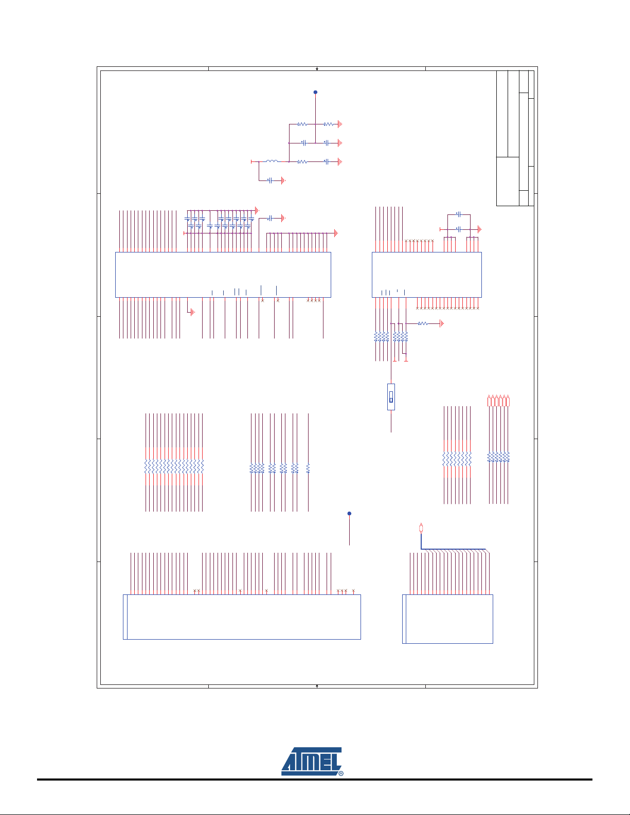
Figure 4-12. CM Board Schematics – 2 of 5
1
DDR2 SDRAM
C53 100nFC53 100nF
C54 100nFC54 100nF
C50 100nFC50 100nF
C48 100nFC48 100nF
C51 100nFC51 100nF
C52 100nFC52 100nF
C47 100nFC47 100nF
C49 100nFC49 100nF
A9
C9
C1
R1
J1
VDD
VDDL
VDDQ
VDDQC3VDDQC7VDDQ
VDDQ
CKEK2CKJ8CKK8CASL7RASK7WE
CS
L8
DDR2_NCS1
DDR2_SDCKE
DDR2_SDCK
DDR2_NSDCK
DDR2_D15
DDR2_D2
DDR2_D1
DDR2_D0
DDR2_D4
DDR2_D3
DDR2_D6
DDR2_D5
2
DQ0G8DQ1G2DQ2H7DQ3H3DQ4H1DQ5H9DQ6F1DQ7
DDR2 SDRAM
DDR2 SDRAM
MT47H64M16HR
MT47H64M16HR
A0M8A1M3A2M7A3N2A4N8A5N3A6N7A7P2A8P8A9P3A10M2BA0L2ODT
MN5
MN5
EBI_A3
EBI_A4
EBI_A5
EBI_A6
EBI_A7
EBI_A8
EBI_A2
3
DDR2_D7
DDR2_D8
F9
DQ8C8DQ9
EBI_A10
EBI_A9
DDR2_D0
DDR2_D1
DDR2_D9
DDR2_D10
DDR2_D11
DDR2_D12
C2
DQ10D7DQ11D3DQ12D1DQ13D9DQ14B1DQ15
A11P7BA1L3A12R2BA2
EBI_A11
EBI_SDA10
EBI_A13
EBI_A14
DDR2_D2
DDR2_D3
DDR2_D4
DDR2_D5
C46 100nFC46 100nF
C44 100nFC44 100nF
C45 100nFC45 100nF
DDR2_D13
DDR2_D15
DDR2_D14
VDDIOM
M9
E1
A1
B9
VDDJ9VDD
VDD
VDD
L1
K9
EBI_A16
EBI_A17
EBI_A18
DDR2_D6
DDR2_D7
DDR2_D8
DDR2_D9
DDR2_D10
DDR2_D11
DDR2_D12
DDR2_D13
DDR2_D14
Evaluation Kit Hardware
25Thursday,November 04,2010Zhu Xueliang
25Thursday,November 04,2010Zhu Xueliang
SMD
SMD
TP23
TP23
DDR_VREF
R34
1.5K 1%
R34
1.5K 1%
R39
1.5K 1%
R39
1.5K 1%
C64
104
C64
104
C62
104
C62
104
L7
10uH
150mAL710uH
150mA
VDDIOM
C61
4.7uF
C61
4.7uF
C58 100nFC58 100nF
C59 100nFC59 100nF
C55 100nFC55 100nF
C56 100nFC56 100nF
C57 100nFC57 100nF
C60
100nF
C60
100nF
DDR_VREF
E9
G9
G3
J2
VDDQ
VDDQG1VDDQG7VDDQ
VDDQ
K3
DDR2_DQS1
DDR2_SDWE
DDR2_RAS
DDR2_CAS
DDR2_DQM0
DDR2_DQM1
DDR2_DQS0
VREF
UDQSB7UDQS
A8
DDR2_DQS1
B2
E3
J3
N1
P9
VSSA3VSS
VSS
VSS
VSS
VSSQ
LDM
UDMB3LDQSE8LDQS
F3
F7
DDR2_DQM0
DDR2_DQM1
DDR2_DQS0
DDR2_SDCKE
DDR2_SDWE
DDR2_SDCK
DDR2_RAS
DDR2_CAS
R331RR33
1R
VSSQD8VSSQE7VSSQF2VSSQ
VSSQD2VSSQA7VSSQB8VSSQH2VSSQ
RFU1A2RFU2
DDR2_NCS1
DDR2_NSDCK
C63
4.7uF
C63
4.7uF
NAND FLASH
C66
C66
100nF
100nF
C65
C65
100nF
NAND_FSH_ D2
NAND_FSH_ D4
NAND_FSH_ D3
NAND_FSH_ D6
NAND_FSH_ D7
NAND_FSH_ D5
NAND_FSH_ D0
NAND_FSH_ D1
F8
H8
J7
VSSDL
RFU3
RFU4R7RFU5
E2
R3
R8
EBI_A15
29
31
41
28
33
45
40
27
I/O0
I/O130I/O332I/O2
I/O744I/O643I/O542I/O4
I/O8_N.C26I/O9_N.C
I/O10_N.C
I/O11_N.C
I/O12_N.C
MN11
MN11
WE
CE9RE
WP19N.C5
N.C11N.C22N.C33N.C4
R/B
ALE
CLE
8
7
17
16
18
REWECERBCLE
ALE
R40 0RR40 0R
R43 0RR43 0R
R44 0RR44 0R
R41 0RR41 0R
R46 470KR46 470K
PD3
PD2
PD0
PD1
VDDNF
ON
ON
1
1
SW1A
SWITCH-2-1.27mm
SW1A
SWITCH-2-1.27mm
1 4
PD4
4
WP
R49
R49
DNP
DNP
R48 470KR48 470K
R47 470KR47 470K
R42 0RR42 0R
PD5
VDDNF
100nF
VDDNF
34
39
25
48
36
13
37
12
VSS
VSS
VCC
VCC
VSS_N.C
VSS_N.C
VCC_N.C
VCC_N.C
I/O15_N.C47I/O14_N.C46I/O13_N.C
N.C6
N.C11
DNU121DNU2
N.C1223N.C13
N.C14
N.C811N.C710N.C914N.C10
6
5
NAND_FSH_ D0
NAND_FSH_ D1
DNU3
MT29F2G08AAD
MT29F2G08AAD
20
22
24
35
38
15
NANDCLE {5}
NANDALE {5}
NANDWE {5}
NANDOE {5 }
NAND_FSH_ D2
NAND_FSH_ D3
NAND_FSH_ D4
NAND_FSH_ D5
NAND_FSH_ D6
NAND_FSH_ D7
25Thursday,November 04,2010Zhu Xueliang
1
MBC-SAM9X5
MBC-SAM9X5
MBC-SAM9X5
Title:
Title:
Title:
Date: Sheet: of
Date: Sheet: of
Date: Sheet: of
AT91SAM9G45-II&DDR2&NANDFLASH A
AT91SAM9G45-II&DDR2&NANDFLASH A
AT91SAM9G45-II&DDR2&NANDFLASH A
A3
A3
A3
Size: Document Number: Rev:
Size: Document Number: Rev:
Size: Document Number: Rev:
Draw By:
Draw By:
Draw By:
2
3
NANDCS {5}
NANDR_B {5}
4
5
RR1BRR1B
2 7
EBI_D0
EBI_D2
EBI_D4
EBI_D3
EBI_D0
EBI_D1
D14D1D15D2A16D3B16D4A17D5B15D6C14D7B14D8A15D9C15
D0
SAM9x5_LBGA217 - EBI
SAM9x5_LBGA217 - EBI
MN2F
MN2F
RR17CRR17C
RR17ARR17A
RR16CRR16C
RR16ARR16A
RR17DRR17D
RR17BRR17B
RR16DRR16D
RR16BRR16B
R50 0RR50 0R
R51 0RR51 0R
R52 0RR52 0R
R53 0RR53 0R
R54 0RR54 0R
PD19
PD18
PD20
J17
K16
K17
PD18/D28/A25
PD19/D29/NCS2
PD20/D30/NCS4
A A
(NANDOE )
(NANDWE )
(NANDAL E)
(NANDCLE )
(NANDCS )
PD3
PD0
PD1
PD4
PD2
PD21
J16
PD21/D31/NCS5
R55 0RR55 0R
(NANDR/B)
4
PD6
5
3 6
1 8
3 6
1 8
4 5
2 7
4 5
PD6
N14
PD6/D16
PD7
R15
PD6
PD8
PD9
M14
N16
PD7/D17
PD8/D18
PD7
PD8
PD11
PD10
N17
N15
PD9/D19
PD10/D20
PD9
PD10
PD13
PD12
K15
M15
PD11/D21
PD12/D22
2 7
PD11
PD12
PD14
PD15
L14
M16
PD13/D23
PD14/D24
PD15/D25/A20
PD13
PD16
PD17
L16
L15
PD16/D26/A23
PD17/D27/A24
RR2ARR2A
RR1CRR1C
RR1ARR1A
RR2CRR2C
RR1DRR1D
1 8
3 6
1 8
3 6
4 5
EBI_D1
EBI_D2
EBI_D3
EBI_D4
EBI_D5
EBI_D6
EBI_D7
EBI_D8
EBI_D5
EBI_D9
D D
RR3ARR3A
RR2BRR2B
2 7
EBI_D6
EBI_D10
D12
D10
RR4CRR4C
RR2DRR2D
RR3DRR3D
RR4BRR4B
RR4ARR4A
RR3BRR3B
RR3CRR3C
RR4DRR4D
1 8
3 6
4 5
4 5
2 7
1 8
2 7
3 6
4 5
EBI_D7
EBI_D8
EBI_D9
EBI_D10
EBI_D11
EBI_D12
EBI_D13
EBI_D14
EBI_D15
EBI_A2
EBI_A3
EBI_A4
EBI_A5
H16
H15A3H17A4G17A5G16A6F17A7E17A8F16A9G15
A2
A0/NBS0
EBI_A8
EBI_A6
EBI_A7
EBI_D11
EBI_D12
EBI_D15
EBI_D14
EBI_D13
C13
A14
B13
A13
C12
J15
D11
D12
D13
D14
D15
A1/NBS2/DQM2/NWR2
R28 27RR28 27R
R35 27RR35 27R
R29 27RR29 27R
R36 27RR36 27R
R30 27RR30 27R
R37 27RR37 27R
R32 27RR32 27R
R31 27RR31 27R
R26 27RR26 27R
R27 27RR27 27R
EBI_DQM1
EBI_DQM0
EBI_DQS0
EBI_RAS
EBI_DQS1
EBI_CAS
EBI_A9
EBI_A10
EBI_A11
EBI_A14
EBI_A13
EBI_A18
EBI_A16
EBI_A17
EBI_A15
EBI_DQM0
G14
F15
D17
C17
E16
D16
E14
C16
B17
E15
A10
A10
A11
A12
A13
A14
A15
A19
DQM0
A16/BA0
A17/BA1
A18/BA2
C C
R38 27RR38 27R
EBI_SDCKE
EBI_SDCK
EBI_NSDCK
EBI_SDWE
EBI_NCS1_SDCS
EBI_SDCKE
EBI_DQM1
EBI_DQS0
A11
B10
DQS0
DQM1
EBI_SDCK
EBI_NSDCK
EBI_RAS
EBI_DQS1
EBI_CAS
EBI_SDWE
EBI_SDA10
A9
DQS1
C11
B12
D11
C8
B11
C10
A12
RAS
CAS
SDCK
SDWE
SDA10
#SDCK
SDCKE
NCS0
EBI_NCS1_SDCS
B9
B8
NCS0
C7
C9
NCS1/SDCS
NWR0/NWRE
SMD
SMD
TP24
TP24
NCS0
D9
A8
NRD
NWR1/NBS1
NWR3/NBS3/DQM3
PD[5..21] {3,5}
(NANDOE )
(NANDWE )
(NANDAL E)
(NANDCLE )
(NANDCS )
PD4
PD5
PD0
PD1
PD2
PD3
P14
R13
P15
P12
P13
R14
PD4/NCS3
PD5/NWAIT
PD0/NANDOE
PD1/NANDWE
PD2/A21/NANDALE
PD3/A22/NANDCLE
SAM9x5_LBGA217 - PIOD
SAM9x5_LBGA217 - PIOD
MN2E
MN2E
B B
Evaluation Kit (EK) User Guide 4-17
11115A–ATARM–27-Jul-11
Page 29
Evaluation Kit Hardware
Figure 4-13. CM Board Schematics – 3 of 5
1
DDR2 SDRAM
C53 100nFC53 100nF
C54 100nFC54 100nF
C50 100nFC50 100nF
C48 100nFC48 100nF
C51 100nFC51 100nF
C52 100nFC52 100nF
C47 100nFC47 100nF
C49 100nFC49 100nF
J1
A9
C9
C1
R1
VDD
VDDL
VDDQ
VDDQC3VDDQC7VDDQ
VDDQ
CKEK2CKJ8CKK8CASL7RASK7WE
CS
L8
DDR2_NCS1
DDR2_SDCKE
DDR2_SDCK
DDR2_NSDCK
DDR2_D15
DDR2_D2
DDR2_D1
DDR2_D0
DDR2_D4
DDR2_D3
DDR2_D6
DDR2_D5
2
DQ0G8DQ1G2DQ2H7DQ3H3DQ4H1DQ5H9DQ6F1DQ7
DDR2 SDRAM
DDR2 SDRAM
MT47H64M16HR
MT47H64M16HR
A0M8A1M3A2M7A3N2A4N8A5N3A6N7A7P2A8P8A9P3A10M2BA0L2ODT
MN5
MN5
EBI_A3
EBI_A4
EBI_A5
EBI_A6
EBI_A7
EBI_A8
EBI_A2
3
DDR2_D7
DDR2_D8
F9
DQ8C8DQ9
EBI_A10
EBI_A9
DDR2_D0
DDR2_D1
DDR2_D9
DDR2_D10
DDR2_D11
DDR2_D12
C2
DQ10D7DQ11D3DQ12D1DQ13D9DQ14B1DQ15
A11P7BA1L3A12R2BA2
EBI_A11
EBI_SDA10
EBI_A13
EBI_A14
DDR2_D2
DDR2_D3
DDR2_D4
DDR2_D5
C46 100nFC46 100nF
C44 100nFC44 100nF
C45 100nFC45 100nF
DDR2_D13
DDR2_D15
DDR2_D14
VDDIOM
B9
M9
E1
A1
VDDJ9VDD
VDD
VDD
L1
K9
EBI_A16
EBI_A17
EBI_A18
DDR2_D6
DDR2_D7
DDR2_D8
DDR2_D9
DDR2_D10
DDR2_D11
DDR2_D12
DDR2_D13
DDR2_D14
C55 100nFC55 100nF
C56 100nFC56 100nF
E9
VDDQ
VDDQG1VDDQG7VDDQ
DDR2_RAS
DDR2_CAS
VDDIOM
C58 100nFC58 100nF
C59 100nFC59 100nF
C57 100nFC57 100nF
J2
G9
G3
VDDQ
K3
DDR2_SDWE
DDR2_DQM0
DDR2_DQM1
L7
10uH
150mAL710uH
150mA
C61
4.7uF
C61
4.7uF
C60
100nF
C60
100nF
DDR_VREF
E3
J3
N1
P9
VSSA3VSS
VSS
VSS
VSS
VREF
UDQSB7UDQSA8LDM
F7
DDR2_DQS1
DDR2_DQS0
DDR2_SDCKE
DDR2_SDWE
DDR2_RAS
DDR2_CAS
DDR2_DQS1
DDR2_DQS0
B2
VSSQ
UDMB3LDQSE8LDQS
F3
DDR2_DQM0
DDR2_DQM1
DDR2_SDCK
DDR2_NSDCK
SMD
SMD
TP23
TP23
DDR_VREF
R34
1.5K 1%
R34
1.5K 1%
C62
104
C62
104
R331RR33
1R
F8
H8
VSSQD8VSSQE7VSSQF2VSSQ
VSSQD2VSSQA7VSSQB8VSSQH2VSSQ
RFU1A2RFU2
RFU3
RFU4R7RFU5
E2
R3
R8
EBI_A15
DDR2_NCS1
25Thursday,November 04,2010Zhu Xueliang
25Thursday,November 04,2010Zhu Xueliang
25Thursday,November 04,2010Zhu Xueliang
R39
1.5K 1%
R39
1.5K 1%
C64
104
C64
104
C63
4.7uF
C63
4.7uF
NAND FLASH
C66
C66
100nF
100nF
C65
C65
100nF
NAND_FSH_ D2
NAND_FSH_ D4
NAND_FSH_ D3
NAND_FSH_ D6
NAND_FSH_ D7
NAND_FSH_ D5
NAND_FSH_ D0
NAND_FSH_ D1
J7
VSSDL
29
I/O0
MN11
MN11
CLE
16
R40 0RR40 0R
PD3
27
31
41
28
33
45
40
I/O130I/O332I/O2
I/O744I/O643I/O542I/O4
I/O8_N.C26I/O9_N.C
I/O10_N.C
I/O11_N.C
I/O12_N.C
WE
CE9RE
WP
N.C11N.C22N.C33N.C4
R/B
ALE
8
7
18
17
REWECERBCLE
ALE
R43 0RR43 0R
R44 0RR44 0R
R41 0RR41 0R
R46 470KR46 470K
PD2
PD0
PD1
VDDNF
ON
ON
1
1
SW1A
SWITCH-2-1.27mm
SW1A
SWITCH-2-1.27mm
1 4
PD4
4
19
WP
R49
R49
DNP
DNP
R48 470KR48 470K
R47 470KR47 470K
R42 0RR42 0R
PD5
VDDNF
100nF
VDDNF
34
39
25
48
36
13
37
12
VSS
VSS
VCC
VCC
VSS_N.C
VSS_N.C
VCC_N.C
VCC_N.C
I/O15_N.C47I/O14_N.C46I/O13_N.C
N.C6
N.C11
N.C5
6
5
N.C811N.C710N.C914N.C10
NAND_FSH_ D0
NAND_FSH_ D1
DNU121DNU2
N.C1223N.C13
N.C14
DNU3
MT29F2G08AAD
MT29F2G08AAD
20
22
24
35
38
15
NANDCS {5}
NANDCLE {5}
NANDALE {5}
NANDWE {5}
NANDOE {5 }
NAND_FSH_ D2
NAND_FSH_ D3
NAND_FSH_ D4
NAND_FSH_ D5
NAND_FSH_ D6
NAND_FSH_ D7
1
MBC-SAM9X5
MBC-SAM9X5
MBC-SAM9X5
Title:
Title:
Title:
Date: Sheet: of
Date: Sheet: of
Date: Sheet: of
AT91SAM9G45-II&DDR2&NANDFLASH A
AT91SAM9G45-II&DDR2&NANDFLASH A
AT91SAM9G45-II&DDR2&NANDFLASH A
A3
A3
A3
Size: Document Number: Rev:
Size: Document Number: Rev:
Size: Document Number: Rev:
Draw By:
Draw By:
Draw By:
2
3
NANDR_B {5}
4
5
RR1BRR1B
2 7
EBI_D0
EBI_D2
EBI_D4
EBI_D3
EBI_D0
EBI_D1
D14D1D15D2A16D3B16D4A17D5B15D6C14D7B14D8A15D9C15
D0
SAM9x5_LBGA217 - EBI
SAM9x5_LBGA217 - EBI
MN2F
MN2F
RR17CRR17C
RR17ARR17A
RR16CRR16C
RR16ARR16A
RR17DRR17D
RR17BRR17B
RR16DRR16D
RR16BRR16B
R50 0RR50 0R
R51 0RR51 0R
R52 0RR52 0R
R53 0RR53 0R
R54 0RR54 0R
PD19
PD18
PD20
J17
K16
K17
PD18/D28/A25
PD19/D29/NCS2
PD20/D30/NCS4
A A
(NANDOE )
(NANDWE )
(NANDAL E)
(NANDCLE )
(NANDCS )
PD3
PD0
PD1
PD4
PD2
PD21
J16
PD21/D31/NCS5
R55 0RR55 0R
(NANDR/B)
4
PD6
5
3 6
1 8
3 6
1 8
4 5
2 7
4 5
PD6
N14
PD5/NWAIT
PD7
PD8
R15
M14
PD6/D16
PD7/D17
PD6
PD7
PD9
PD10
N16
N17
PD8/D18
PD9/D19
PD8
PD9
PD12
PD11
N15
K15
PD10/D20
PD11/D21
PD12/D22
2 7
PD10
PD11
PD14
PD13
M15
L14
PD13/D23
PD12
PD13
PD15
PD16
M16
L16
PD14/D24
PD15/D25/A20
PD16/D26/A23
PD17
L15
PD17/D27/A24
RR2ARR2A
RR1CRR1C
RR1ARR1A
RR2CRR2C
RR1DRR1D
1 8
3 6
1 8
3 6
4 5
EBI_D1
EBI_D2
EBI_D3
EBI_D4
EBI_D5
EBI_D6
EBI_D7
EBI_D8
EBI_D5
EBI_D9
D D
RR3ARR3A
RR2BRR2B
2 7
EBI_D6
EBI_D10
D12
D10
RR4CRR4C
RR2DRR2D
RR3DRR3D
RR4BRR4B
RR4ARR4A
RR3BRR3B
RR3CRR3C
RR4DRR4D
1 8
3 6
4 5
4 5
2 7
1 8
2 7
3 6
4 5
EBI_D7
EBI_D8
EBI_D9
EBI_D10
EBI_D11
EBI_D12
EBI_D13
EBI_D14
EBI_D15
EBI_A2
EBI_A3
EBI_A4
J15
H16
H15A3H17A4G17A5G16A6F17A7E17A8F16A9G15
A2
A0/NBS0
EBI_A8
EBI_A5
EBI_A6
EBI_A7
EBI_D11
EBI_D12
EBI_D15
EBI_D14
EBI_D13
C13
A14
B13
A13
C12
D11
D12
D13
D14
D15
A1/NBS2/DQM2/NWR2
R28 27RR28 27R
R35 27RR35 27R
R29 27RR29 27R
R36 27RR36 27R
R30 27RR30 27R
R37 27RR37 27R
R32 27RR32 27R
R31 27RR31 27R
R26 27RR26 27R
R27 27RR27 27R
EBI_DQM1
EBI_DQM0
EBI_DQS0
EBI_RAS
EBI_DQS1
EBI_CAS
EBI_A9
EBI_A10
EBI_A11
EBI_A14
EBI_A13
EBI_A18
EBI_A16
EBI_A17
EBI_A15
EBI_DQM0
G14
F15
D17
C17
E16
D16
E14
C16
B17
E15
A10
A10
A11
A12
A13
A14
A15
A19
DQM0
A16/BA0
A17/BA1
A18/BA2
C C
R38 27RR38 27R
EBI_SDCKE
EBI_SDCK
EBI_NSDCK
EBI_SDWE
EBI_NCS1_SDCS
EBI_SDCKE
EBI_DQM1
EBI_DQS0
B10
A11
DQS0
DQM1
EBI_SDCK
EBI_NSDCK
EBI_RAS
EBI_DQS1
EBI_CAS
EBI_SDWE
EBI_SDA10
C11
B12
D11
C8
B11
C10
A12
A9
RAS
CAS
DQS1
SDCK
SDWE
SDA10
#SDCK
SDCKE
NCS0
EBI_NCS1_SDCS
B9
B8
NCS0
C7
C9
NCS1/SDCS
NWR0/NWRE
SMD
SMD
TP24
TP24
NCS0
D9
A8
NRD
NWR1/NBS1
NWR3/NBS3/DQM3
PD[5..21] {3,5}
(NANDOE )
(NANDWE )
(NANDAL E)
(NANDCLE )
(NANDCS )
PD4
PD5
PD0
PD1
PD2
PD3
P14
R13
P15
P12
P13
R14
PD4/NCS3
PD0/NANDOE
PD1/NANDWE
PD2/A21/NANDALE
PD3/A22/NANDCLE
SAM9x5_LBGA217 - PIOD
SAM9x5_LBGA217 - PIOD
MN2E
MN2E
B B
4-18 Evaluation Kit (EK) User Guide
11115A–ATARM–27-Jul-11
Page 30

Figure 4-14. CM Board Schematics – 4 of 5
Evaluation Kit Hardware
45Thursday,November 04,2010Zhu Xueliang
45Thursday,November 04,2010Zhu Xueliang
45Thursday,November 04,2010Zhu Xueliang
1
ETH0_RX+ {5}
ETH0_TX+ {5}
GND_ETH
R72
49.9R1%
R72
49.9R1%
C72 100nFC72 100nF
R71
R71
49.9R1%
49.9R1%
2
43
7
8
XT1
TX+
3
REF_CLK/XT2
TX_EN
TXD317TXD218TXD020TXD119TX_CLK/ISOLATE22RXD0/PHYAD029RXD1/PHYAD128RXD2/PHYAD227RXD3/PHYAD3
MN10
MN10
42
21
C71
100nF
C71
100nF
VDDANA
41
32
VDD
VDD
R70
10K
R70
10K
50MHz
50MHz
VSS OUT
OE
VSS OUT
OE
Y3
Y3
4
R74 22RR74 22R
TP27
SMD
TP27
SMD
ETH0_RX- {5}
ETH0_TX- {5}
R84
49.9R1%
R84
49.9R1%
C78
100nF
C78
100nF
R83
R83
49.9R1%
49.9R1%R86 1.5KR86 1.5K
SMD
SMD
TP28
TP28
C76
10uF+C76
10uF
+
AVDDT
C75
10uF+C75
10uF
+
C74 100nFC74 100nF
AVDDT
2
DM9161AE P
DM9161AE P
CRS/PHYAD435MDIO25MDINTR
24
VDDANA
VDDANA
C77 100nFC77 100nF
9
6
46
AGND5AGND
AVDDT
DISMDIX39DVDD30DVDD
32
VDDANA
AGND
5
6
7
8
6
7
8
B1
BLM21BD222TN1B1BLM21BD222TN1
C73 100nFC73 100nF
3
4
TX-
RX-
RX+
AVDDR1AVDDR
TX_ER/TXD416COL/RMII36MDC
RX_CLK/10BTSER34RX_DV/TESTMODE37RX_ER/RXD4/RPTR
26
38
GND_ETHGND_ETH
6
7
8
R96 0RR96 0R
47
BGRESG
DVDD
41
C79 100nFC79 100nF
RR9
RR9
R98
R98
R97
R97
C80 100nFC80 100nF
10KX4
10KX4
10K
10K
6.8K
6.8K
23
C81 100nFC81 100nF
R95 DNPR95 DNP
R
94 10KR94 10K
R93 1 0KR93 1 0K
R
92 4.7KR92 4.7K
91 DNPR91 DNP
R
4
3
2
1
4 5
3
2
1
LED0 {5}
4 5
3
2
1
31
11
48
BGRES
LEDMODE
DGND33RESET
15
RR8
RR8
10KX4
10KX4
RR7
RR7
10KX4
10KX4
LED1 {5}
LED2 {5}
13
LED1/OP112LED0/OP0
DGND44DGND
VDDANA
45
14
LED2/OP2
CABLESTS/LINKSTS
PWRDWN
40
10
R99 0RR99 0R
N.C
GND_ETH
R1000RR100
0R
C82
10uF+C82
10uF
+
VDDANA
NRST{1,5}
ETHERNET
1
MBC-SAM9X5
MBC-SAM9X5
MBC-SAM9X5
Title:
Title:
Title:
Date: Sheet: of
Date: Sheet: of
Date: Sheet: of
ETHERNET A
ETHERNET A
ETHERNET A
A3
A3
A3
Size: Document Number: Rev:
Draw By:
Draw By:
Draw By:
Size: Document Number: Rev:
Size: Document Number: Rev:
2
3
4
RR14CRR14C
RR13BRR13B
RR14DRR14D
RR13CRR13C
RR13DRR13D
2 7
3 6
4 5
R73 22RR73 22R
E0_TX1
E0_TX0
E0_TXEN
E0_TXCK
PB4
PB10
PB9
PB7
5
PB[0..18]{3,5}
D D
RR15BRR15B
3 6
4 5
2 7
E0_RX1
E0_RX0
E0_RXDV
PB1
PB0
PB3
C C
RR15ARR15A
RR14BRR14B
RR15CRR15C
RR14ARR14A
1 8
2 7
3 6
1 8
E0_MDC
E0_MDIO
E0_INTR
E0_RXER
PB2
PB6
PB5
PB8
5
Install as need to
alter PHYaddress,
must override internal
pullup on SAM9x5
B B
A A
Evaluation Kit (EK) User Guide 4-19
11115A–ATARM–27-Jul-11
Page 31

Evaluation Kit Hardware
Figure 4-15. CM Board Schematics – 5 of 5
55Thursday,November 04,2010Zhu Xueliang
55Thursday,November 04,2010Zhu Xueliang
55Thursday,November 04,2010Zhu Xueliang
PD15
PD14
PD[5..21] {2,3}
PD9
PD8
PD11
PD10
PD13
PD12
PD17
PD16
PD19
PD18
PD20
PD15
PD14
PD5
PD7
C86
4.7uF
C86
4.7uF
PA6
PA21
PA23
PA30
PA15
PA17
PA19
PA12
PA14
PA7
PA1
PA3
PD17
PD19
PD21
90
92
100
94
96
98
88
82
84
86
PA1
PA3
GND
PA12
PA14
PD17
PD19
PD21
VDDIOP0
PD16
PD18
PD20
VDDIOP 0
PA0
PA2
PA4
PA11
81
PD16
PA13
83
85
87
89
91
93
95
97
PA0
PA2
PA4
PA11
PD18
PD20
PA13
116
114
102
104
106
108
110
112
PA7
PA6
GND
PA21
PA23
PA30
PA15
PA17
PA19
GND
PA8
PA22
PA31
GND
PA16
PA18
PA20
99
PA5
101
103
105
107
109
111
113
115
PA8
PA22
PA31
PA16
PA18
PA20
PA5
PD21
R1020RR102
R101
R101
0R
DNP
DNP
+3V3
C87
4.7uF
C87
4.7uF
VDDIOP1VDDIOP1
PC23
PC25
PC27
PC28
PC13
PC15
PC1
PC3
PC5
PC6
PC8
PA9
PA24
PA26
118
120
122
PA9
PA24
PA26
PA10
GND
PA25
117
119
121
PA10
PA25
PC10
PA28
126
142
130
132
134
136
138
124
128
140
144
146
PC1
PC3
PC5
PC6
PC8
GND
PA28
PA27
123
125
PA27
PA29
GND
PC10
PC13
VDDIOP1
PA29
VDDIOP 1
127
129
PC0
PC15
PC0
PC2
PC4
GND
PC7
PC9
PC11
PC12
PC14
131
133
135
137
139
141
143
145
PC2
PC4
PC7
PC9
PC11
PC12
PC14
PC30
PC16
PC18
PC20
154
148
150
152
156
158
160
162
164
GND
PC16
PC18
PC20
PC23
PC25
PC27
PC28
PC30
GND
PC17
PC19
PC21
PC22
PC24
PC26
GND
147
PC29
149
151
153
155
157
159
161
163
PC17
PC19
PC21
PC22
PC24
PC26
PC29
C88
C88
1uF
1uF
ADVREF
PB1
PB3
PB5
PB7
VDDANAVDDANA
166
170
172
174
176
168
PB1
PB3
PB5
VDDANA
SELCONFIG0
PC31
VDDANA
PB0
PB2
PB4
165
167
169
171
173
175
PC31
PB0
PB2
PB4
PB6
LED0 {4}
LED1 {4}
LED2 {4}
PB12
PB11
AVDDT
PB14
PB16
198
190
200
184
186
188
192
194
196
PB14
PB16
LED0
LED1
LED2
AVDDT
ADVREF
GNDANA
GND_ETH
PB13
PB15
PB17
PB18
GND
ETH0_TX+
ETH0_TX-
ETH0_RX+
183
PB13
ETH0_RX-
185
187
189
191
193
195
197
199
PB15
PB17
PB18
PB10
PB12
180
182
178
PB7
PB10
GNDANA
PB6
PB8
PB9
177
179
181
PB8
PB9
PB11
1
MBC-SAM9X5
MBC-SAM9X5
MBC-SAM9X5
Title:
Title:
Title:
Date: Sheet: of
Date: Sheet: of
Date: Sheet: of
AT91SAM9G45-II A
AT91SAM9G45-II A
AT91SAM9G45-II A
A3
A3
A3
Size: Document Number: Rev:
Size: Document Number: Rev:
Size: Document Number: Rev:
Draw By:
Draw By:
Draw By:
2
GND_ETH
3
PIO200-pinSODIMMJ1PIO200-pinSODIMM
1
2
NANDWE {2}
4.7uF
4.7uF
52
RFU18
RFU17
51
NANDCLE {2}
PD11
PD13
PD15
PD7
PD9
PD5
74
64
66
68
70
54
GND
RFU20
GND
RFU19
53
72
56
58
60
62
76
78
80
PD1
PD3
PD5
PD7
PD9
GND
PD11
VDDNF
VDDNF
63
PD13
PD0
PD2
PD4
PD6
PD8
NC
PD10
PD12
65
67
69
71
73
75
77
79
PD10
PD12
PD14
PD8
RFU22
RFU24
RFU26
RFU21
RFU23
RFU25
55
57
59
61
WKUP {1}
BMS {1}
NTRST {1}
TDI {1}
TCK {1}
TMS {1}
SHDN {1}
TDO {1}
RTCK {1}
PWR_EN {1}
NRST {1,4}
C85
C84
C84
1uF
1uF
VDDBU
+3V3
12
2
4
3
VCC_3V3
VCC_3V3
VCC_3V3
VCC_3V3
J1
1
3
+3V3
C83
10uF
C83
10uF
6
5
8
VBAT
JTAGSEL
GND
USBC_DP
7
10
WKUP
USBC_DM
9
11
14
SHDN
GND
13
18
16
BMS
nRST
nTRST
USBB_DM
USBB_DP
GND
15
17
22
24
26
28
30
20
32
34
TDI
TCK
TMS
TDO
RFU2
RFU4
RTCK
PWR_EN
DIBP
DIBN
GND
USBA_DM
USBA_DP
GND
RFU1
RFU3
19
21
23
25
27
29
31
33
C85
VDDNF
42
40
44
46
48
50
36
38
GND
RFU6
RFU8
RFU10
RFU12
RFU14
RFU16
RFU5
RFU7
RFU9
GND
RFU11
RFU13
RFU15
35
37
39
41
43
45
47
49
VDDNF
4
5
DIBP{1}
DIBN{1}
HHSDPC{1} JTAGSEL {1}
HHSDMC{1}
HHSDPB{1}
HHSDMB{1}
HHSDPA{1}
HHSDMA{1}
PA0
PA1
PA3
PA2
PA5
PA7
PA6
PA4
PA9
PA11
PA10
PA13
PA15
PA14
PA12
PA8
PA[0..31]{3}
D D
PA17
PA19
PA18
PA16
NANDOE{2}
NANDALE{2}
NANDCS{2}
NANDR_B{2}
VDDIOP0 VDDIOP0
PA21
PA23
PA22
PA20
PA25
PA27
PA26
PA29
PA31
PA30
PA28
PA24
PB1
PB2
PB3
PB6
PB7
PB5
PB4
PB9
PB15
PB13
PB10
PB11
PB8
PB12
PB14
PB18
PB17
PB0
PB[0..18]{3,4}
C C
PB16
PC1
PC2
PC3
PC6
PC7
PC5
PC4
PC9
PC15
PC13
PC12
PC10
PC11
PC8
PC14
PC21
PC18
PC19
PC17
PC20
PC22
PC23
PC0
PC[0..31]{3}
B B
PC16
ETH0_TX+{4}
ETH0_TX-{4}
ETH0_RX+{4}
ETH0_RX-{4}
PC25
PC31
PC29
PC26
PC27
PC24
PC28
PC30
A A
4
5
4-20 Evaluation Kit (EK) User Guide
11115A–ATARM–27-Jul-11
Page 32

4.3 EK Board Description
4.3.1 EK Board Overview
The EK board serves as the main board that carries the CPU module. It features all necessary peripherals and interfaces for processor evaluation.
Figure 4-16. Commented EK Board Layout
Evaluation Kit Hardware
Evaluation Kit (EK) User Guide 4-21
11115A–ATARM–27-Jul-11
Page 33

Evaluation Kit Hardware
4.3.2 Equipment List
Based on the processor installed on the CM board, the EK board is equipped with the following interfaces or peripherals:
4.3.2.1 Devices
List of the EK board peripherals:
Two EMAC PHY
One Audio codec
Two high speed MCI Card interfaces
Two CAN transceivers
Three RS232 ports with level translator features: DBGU, USART0 and USART3
One Smart DAA port
Two USB host ports
One USB host/device port
On-board power regulation
LCD/ISI extension interface
ZigBee
One-wire device
®
interface
4.3.2.2 Board Interface Connection
Main power supply (J4)
One SODIMM200 socket (CON1)
USB A Host/Device, support USB host/device using a type micro AB connector (J20)
USB B Host, support USB host using a type A connector (J19, upper)
USB C Host, support USB host using a type A connector (J19, lower)
DBGU (RX and TX only) connected to a 9-way male RS232 connector (J11)
USART1 (RX, TX, RTS, CTS) connected to a 9-way male RS232 connector (J8)
USART3 (RX, TX, RTS, CTS) connected to a 9-way male RS232 connector (J12)
JTAG, 20 pin IDC connector (J9)
MicroSD connector (J6)
SD/MMC connector (J7)
Headphone (J15), line-in (J13)
Image sensor connector (J21)
DM board connection for QTouch and TFT LCD display with Touch Screen and backlight (J21, J22)
DAA connecter RJ11 6P4C type (J16)
CAN bus connectors RJ12 6P6C type (CON2, CON3)
ZigBee connector (J10)
Three IO expansion ports (J1, J2, J3)
Test points, various test points are located throughout the board
4.3.2.3 Push Button Switches
Reset, board reset (BP1)
Wake up, push button to bring the processor out of low power mode (BP2)
4-22 Evaluation Kit (EK) User Guide
11115A–ATARM–27-Jul-11
Page 34

4.3.3 Function Blocks
4.3.3.1 Processor
The Evaluation Kit board may be used with any of the Core Modules:
SAM9G15
SAM9G25
SAM9G35
SAM9X25
SAM9X35
Evaluation Kit Hardware
Evaluation Kit (EK) User Guide 4-23
11115A–ATARM–27-Jul-11
Page 35

Evaluation Kit Hardware
Figure 4-17. SODIMM Interface on EK Board
PD10
PD12
PD14
PD16
PD18
PD20
PA0
PA2
PA4
PA11
PA13
PA8
PA22
PA31
PA16
PA18
PA20
PA5
PA10
PA25
PA27
PA29
PC0
PC2
PC4
PC7
PC9
PC11
PC12
PC14
PC17
PC19
PC21
PC22
PC24
PC26
PC29
PC31
VDDAN A
PB0
PB2
PB4
PB6
PB8
PB9
PB11
PB13
PB15
PB17
PB18
3V3
CON1
1
VCC1
3
VCC3
5
GND1
USBC_D P
USBC_D M
USBB_DM
USBB_DP
DIBP
DIBN
USBA_DM
USBA_DP
VDDNF
(MCI1_CD)
ZB_RSTN
EN5V_HDA#
EN5V_HDC#
VDDI OP0
SPI1_NPCS1
TXD0
(MCI1_DA1) (MCI1_DA2)
RTS0
(MCI1_DA3)
(MCI1_DA0)
(MCI1_CK)
(MCI0_CDA) (MCI0_CK)
(MCI0_DA1)
(MCI0_DA3)
TWC K0
ZB_IRQ1
SPI1_MOSI
DTXD
TF
RF
ISI_D0
ISI_D2
ISI_D4
ISI_D7
ISI_D9
ISI_D11
ISI_PCK
ISI_HSYNC
E1_TX1
E1_RX1
TXD3
RTS3
E1_INTR
E1_TXCK
E1_MDIO
E0_RX0
E0_RXER
E0_TXCK
E0_MDC
E0_INTR
E0_TX0 E0_TX1
AD0_XP
AD2_YP
AD4_LR
ONE_WIRE
ETH0_TX+
ETH0_TX-
ETH0_RX+
ETH0_RX-
VDDIOP1
LCDDAT0
LCDDAT2
LCDDAT4
LCDDAT7
LCDDAT9
LCDDAT11
LCDDAT12
LCDDAT14
LCDDAT17
LCDDAT19
LCDDAT21
LCDDAT22
LCDDISP
LCDPWM
LCDDEN
OVCUR_USB
7
USBC_D P
9
USBC_D M
11
GND3
13
USBB_DM
15
USBB_DP
17
GND4
19
DIBP
21
DIBN
23
GND5
25
USBA_DM
27
USBA_DP
29
GND6
31
RFU1
33
RFU3
35
RFU5
37
RFU7
39
RFU9
41
GND7
43
RFU11
45
RFU13
47
RFU15
49
RFU17
51
GND9
53
RFU19
55
RFU21
57
RFU23
59
RFU25
61
VDDNF1
63
PD0
PD0/NANDOE
65
PD2
PD2/A21/NANDALE
67
PD4
PD4/NCS3
69
PD6
PD6/D 16
71
PD8
PD8/D 18
73
NC
75
PD10
PD10/D 20
77
PD12
PD12/D 22
79
PD14
PD14/D 24
81
PD16
PD16/D26/A23
83
PD18
PD18/D28/A25
85
PD20 PD21
PD20/D30/NCS4
87
VDDIOP0_0
89
PA0
PA0/TXD0/SPI1_NPC S1
91
PA2
PA2/RTS0/MCI1_DA1/E0_ETX0
93
PA4
PA4/SCK0/ MCI1_D A3/E0_ETXER
95
PA11
PA11/SPI0_MISO/ MCI1_D A0
97
PA13
PA13/SPI0_SPC K/MCI1_CK
99
GND13
101
PA8
PA8/TIOA0/SPI 1_MISO
103
PA22
PA22/TIOA1/SPI 1_MOSI
105
PA31
PA31/TWCK0/ SPI1_NPCS2/E0_ETXEN
107
GND14
109
PA16
PA16/MCI0_C DA
111
PA18
PA18/MCI0_D A1
113
PA20
PA20/MCI0_D A3
115
PA5
PA5/TXD1/CANTX1
117
PA10
PA10/DTXD/CAN TX0
119
GND15
121
PA25
PA25/TCLK1/TF
123
PA27
PA27/TIOB0/R D
125
PA29
PA29/TIOB2/R F
127
VDDIOP1_0
129
PC0
PC0/LCDDAT0/ISI_D0/TWD1
131
PC2
PC2/LCDDAT2/ISI_D2/TIOA3
133
PC4
PC4/LCDDAT4/ISI_D4/TCLK3
135
GND18
137
PC7
PC7/LCDDAT7/ISI_D7/TCLK4
139
PC9
PC9/LCDDAT9/ISI_D9/URXD0
141
PC11
PC11/LCDDAT11/ISI_D11/PWM1
143
PC12
PC12/LC DDAT12/ISI_PC K/TIOA5
145
PC14
PC14/LCDDAT14/ISI_HSYNC/TCLK5
147
GND20
149
PC17
PC17/LCDDAT17/URXD1
151
PC19
PC19/LC DDAT19/E1_TX1/PWM1
153
PC21
PC21/LCDDAT21/E1_RX1/PWM3
155
PC22
PC22/LC DDAT22/TXD3
157
PC24
PC24/LC DDISP/R TS3
159
PC26
PC26/LC DPWM/SCK3
161
GND22
163
PC29
PC29/LC DDEN/E1_TXCK/SCK1
165
PC31
PC31/FIQ/E1_MDIO/PCK1
167
VDDANA_0
169
PB0
PB0/E0_RX0/RTS2
171
PB2
PB2/E0_RXER/SC K2
173
PB4
PB4/E0_TXCK/TWD2
175
PB6
PB6/E0_MDC/ AD7
177
PB8
PB8/E0_TXER/AD9
179
PB9
PB9/E0_TX0/PCK1/AD10
181
PB11
PB11/E0_TX2/PWM0/AD0
183
PB13
PB13/E0_RX2/PWM2/AD 2
185
PB15
PB15/E0_RXCK/AD 4
187
PB17
PB17/E0_COL/ AD6
189
PB18
PB18/IR Q/ADTRG
191
GND23
193
ETH0_TX+
195
ETH0_TX-
197
ETH0_RX+
199
ETH0_RX-
1612618-4
KEY
PA3/CTS0/MCI 1_DA2/E0_ETX1
PA12/SPI0_MOSI/ MCI1_C DA
PA21/RXD2/SPI 1_NPCS0
PA30/TWD0/ SPI1_NPCS3/E0_EMDC
PC1/LCDDAT1/ISI_D1/TWCK1
PC3/LCDDAT3/ISI_D3/TIOB3
PC5/LCDDAT5/ISI_D5/TIOA4
PC6/LCDDAT6/ISI_D6/TIOB4
PC8/LCDDAT8/ISI_D8/UTXD0
PC10/LCDDAT10/ISI_D10/PWM0
PC13/LCDDAT13/ISI_VSYNC/TIOB5
PC15/LCDDAT15/ISI_MCK
PC16/LCDDAT16/E1_RXER/UTXD1
PC18/LCDDAT18/E1_TX0/PWM0
PC20/LC DDAT20/E1_RX0/PWM2
PC27/LC DVSYNC /E1_TXEN /RST1
PC28/LCDHSYNC/E1_CRSDV/CTS1
PB3/E0_RXDV/SPI 0_NPCS3
PB10/E0_TX1/PCK0/AD11
PB12/E0_TX3/PWM1/AD1
PB14/E0_RX3/PWM3/AD 3
VCC2
VCC4
VBAT
JTAGSEL
WKUP
SHDN
nRST
nTRST
RTCK
PWR_EN
RFU2
RFU4
RFU6
RFU8
RFU10
GND8
RFU12
RFU14
RFU16
RFU18
GND10
RFU20
RFU22
RFU24
RFU26
VDDN F2
PD1/NANDWE
PD3/A22/ NANDCLE
PD5/NWAIT
PD7/D17
PD9/D19
GND11
PD11/D21
PD13/D23
PD15/D 25/A20
PD17/D 27/A24
PD19/D29/NCS2
PD21/D31/NCS5
VDDI OP0_1
PA1/RXD0
GND12
PA14/SPI0_N PCS0
PA7/TXD2
PA23/TIOA2/SPI 1_SPCK
PA15/MCI0_D A0
PA17/MCI0_C K
PA19/MCI0_D A2
GND16
PA6/RXD1/CANRX1
PA9/DRXD/CANRX0
PA24/TCLK0/TK
PA26/TCLK2/TD
PA28/TIOB1/R K
GND17
VDDI OP1_1
GND19
GND21
PC23/LCDDAT23/RXD3
PC25/C TS3
PC30/LC DPCK/E1_MDC
SELCONF IG
VDDANA_1
PB1/E0_RX1/CTS2
PB5/E0_MDIO/ TWCK2
PB7/E0_TXEN/AD8
GNDAN A1
PB16/E0_CRS/AD5
GNDAN A2
ADVREF
LED0
LED1
LED2
AVDDT
GND_ETH
BMS
TDI
TCK
TMS
TDO
2
4
6
8
10
12
14
16
18
20
22
24
26
28
30
32
34
36
38
40
42
44
46
48
50
52
54
56
58
60
62
64
66
68
70
72
74
76
78
80
82
84
86
88
90
92
94
96
98
100
102
104
106
108
110
112
114
116
118
120
122
124
126
128
130
132
134
136
138
140
142
144
146
148
150
152
154
156
158
160
162
164
166
168
170
172
174
176
178
180
182
184
186
188
190
192
194
196
198
200
3V3
BMS
PD1
PD3
PD5
PD7
PD9
PD11
PD13
PD15
(MCI0_CD)
PD17
PD19
EN5V_HDB#
PA1
PA3
PA12
PA14
PA7
ZB_IRQ0
PA21
PA23
SPI1_SPCK
PA30
PA15
PA17
PA19
PA6
PA9
PA24
PA26
PA28
PC1
LCDDAT1
PC3
LCDDAT3
PC5
LCDDAT5
PC6
LCDDAT6
PC8
LCDDAT8
PC10
LCDDAT10
PC13
LCDDAT13
PC15
LCDDAT15
PC16
LCDDAT16
PC18
LCDDAT18
PC20
LCDDAT20
PC23
LCDDAT23
PC25
PC27
LCDVSYNC
PC28
LCDHSYNC
PC30
LCDPCK
PB1
PB3
PB5
PB7
PB10
PCK0
PB12
PB14
PB16
VBUS_SENSE
VDDNF
VDDI OP0
VDDI OP1
VBAT
WAKE UP
SHDN
NRST
NTRST
TDI
TCK
TMS
TDO
RTCK
PWR_EN
RXD0
CTS0
SPI1_MISO
TWD0
DRXDCANTX0
ISI_D1
ISI_D3
ISI_D5
ISI_D6
ISI_D8
ISI_D10
ISI_VSYNC
ISI_MCK
RXD3
CTS3
AD1_XM
AD3_YM
ETH0_LED0
ETH0_LED1
ETH0_LED2
ETH0_AVDDT
ETH0_GND
VDDI OP0
JP9 f or BMS Conf ig:
When Open,BMS=1: Boot on embedded ROM
R83
When Clos e,BMS=0: Boot on Ex ternal m emory
4.7k
ZB_SLPTR
(MCI1_CD A)
(MCI0_DA0)
(MCI0_DA2)
CANRX1CANTX1
CANRX0
TK
TD
RKRD
E1_RXER
E1_TX0
E1_RX0
E1_TXEN
E1_CRSD V
E1_MDC
E0_RX1
E0_RXDV
E0_MDIO
E0_TXEN
JP9
1 2
SIP2
JTAG
PD5
PD9
PD11
PD13
PD15
PD17
PD19
PD21
PA1
PA3
PA12
PA14
PA7
PA21
PA23
PA30
PA15
PA17
PA19
PA6
PA9
PA24
PA26
PA28
PC1
PC3
PC5
PC6
PC8
PC10
PC13
PC15
PC16
PC18
PC20
PC23
PC25
PC27
PC28
PC30
SELCONF IG
VDDANA
PB1
PB3
PB5
PB7
PB10
PB12
PB14
PB16
ADVREF
4-24 Evaluation Kit (EK) User Guide
11115A–ATARM–27-Jul-11
Page 36

4.3.3.2 Power Supplies
The EK Board features one adjustable LDO. It accepts DC 5V power input and outputs a regulated
+3.3V to most other circuits on the board through four 3.3V rails.
VDDPIO0
VDDPIO1
VDDANA
VDDISI
This LDO is enabled through a dual FET scheme. The processor can assert SHDN (which is a VDDBUpowered I/O) to shut down the LDO to enter the so-called backup mode. The regulator on CM board is
also shut down by the action of the SHDN signal.
If the 3V battery is mounted on J5, both CM and EK boards can be woken up by action on the BP2 button, which drives the WKUP signal (also a VDDBU-powered I/O).
Figure 4-18. EK Board Power Management
Evaluation Kit Hardware
VDDI SI
VDDANA
1 2
L1
VOUT =
3V3 3V3
1 2
220ohm at 100MHz
L2
220ohm at 100MHz
R3
470R
12
R2 47k
C5 10n
0.8V x (Rtop + Rbottom)/Rbottom
R1
100k
6
7
8
ADJ
GND
VOUT
PGOOD1EN2VIN3VDD
MN3
RT9018A
5V
POWER_EN
5V
VDDIOP0
VDDIOP1
1 2
L16
5
4
1 2
220ohm at 100MHz
L17
220ohm at 100MHz
D2
Red
3V3
C9
10u
C8
1u
R5
15k
NC
EP
9
C7
1u
C6
10u
456
VBAT
JP4
SIP2
1 2
3
1
D1
BAT54CLT1G
J5
C4
100n
2
Place C22 near MN3. pin2
C22
1u
R8
10k
R7
10k
3V3
PWR_EN
R25
10k
3
Q6
IRLML2402
R4
100k
C120
1u
2
1
Q1
JP5
Si1563EDH
PWR_EN #
12
C57
100n
15p
C10
1 32
SIP2
FORCE
POWER
ON
SHDN
Evaluation Kit (EK) User Guide 4-25
11115A–ATARM–27-Jul-11
Page 37

Evaluation Kit Hardware
There is another 3.3V rail, VDDNF, supplied from the CM board. VDDNF is set to 3.3V in the current CM
design. The processors also support a 1.8V NAND Flash device, in which case VDDNF is set to 1.8V. In
order to avoid potential voltage conflict on user-defined applications, a level shifter is inserted between
the PIO lines on VDDNF rail and the 3.3V application.
Figure 4-19. Level Shifter For VDDNF Rail
4.3.3.3 JTAG/ICE
Software debug is accessed by a standard 20-pin JTAG connection. This allows connection to a standard USB-to-JTAG in-circuit emulator such as SAM-ICE™.
PD17
PD16
PD20
PD19
PD18
VDDN F
MN1 8
1
VCCA
VCCB1
2
DIR
VCCB2
3
A1
4
A2
5
A3
6
A4
7
A5
8
A6
9
A7
10
A8
11
GND1
GND212GND3
SN74AVC8T245PWR
OE
3V3
24
23
22
21
B1
20
B2
19
B3
18
B4
17
B5
16
B6
15
B7
14
B8
13
C119 100nC118 100n
EN5V_HD C#
EN5V_HD B#
EN5V_HD A#
ZB_SLPTR
ZB_RSTN
Figure 4-20. JTAG Interface
VDDI OP0
J9
14
16
18
20
BR20-H
VDDI OP0
12
34
56
78
910
1112
13
15
17
19
VDDI OP0
R46
100k
DNP
R47
R48
100k
100k
DNP
DNP
R54 0R
R49
100k
DNP
DNP
R50 0R
R51 0R
R58
0R
DNP
NTRST
TDI
TMS
TCK
RTCK
TDO
NRST
NTRST
TDI
TMS
TCK
RTCK
TDO
NRST
4-26 Evaluation Kit (EK) User Guide
11115A–ATARM–27-Jul-11
Page 38

4.3.3.4 DBGU
Evaluation Kit Hardware
The UART is connected to the DB-9 male socket through an RS-232 Transceiver (TXD and RXD only).
A jumper, JP11, is used to select DBGU or CAN0 between IO (PA9, PA10) sharing scheme. Close JP11
to select DBGU.
Figure 4-21. DBGU Com Port
VDDI OP0
C31
100n
R72 0R
PWR_EN
1
6
2
7
3
8
4
9
5
10
J11
11
EARTH_RS232
SEL_CAN
PA9
PA10
DTXD
DRXD
R59
100k
VDDIOP0
VDDI OP0
R60
100k
R67 0R
R71 0R
R73 100k
C30
100n
C36
100n
JP11
SIP2
1 2
MN8
2 17
C1+V+VCC
4
5
6
12
11
13
10 9
1 18
GND
C1C2+
C2- V-
T1
T2
R1
R2
EN
ADM3222ARW
SD
16
3
7
15
8
14
C33 100n
C38 100n
Evaluation Kit (EK) User Guide 4-27
11115A–ATARM–27-Jul-11
Page 39

Evaluation Kit Hardware
4.3.3.5 USART
The USART0 and USART3 are used as serial communication ports. Both USARTs are buffered with an
RS-232 Transceiver (TXD, RXD and handshake CTS/RTS control) and connected to the DB-9 male
socket. The software must assign the appropriate PIO pins to enable the USART function.
The USART3 is only supported by SAM9G25 and SAM9X25 processors. The RS-232 Transceiver for
USART3 is enabled by the signal SELCONFIG comprised of a pull down resistor on CM board. Ref to
Section 4.4.1 ”DM Board Overview” for details.
Figure 4-22. USART Com Port
USART0
VDDIOP0
C14
100n
MN4
3
VCC
23
GND
V+1C2+
21
V-
19
SD
5
EN
7
T1IN
8
T2IN
9
T3IN
10
R1OUT
11
R2OUT
R3OUT12R3IN
ADM3312EARU
T1OU T
T2OU T
T3OU T
R1IN
R2IN
6
C16 100n
C1+
20
C1-
2
C17 100n
4
C2-
24
C19 100n
C3+
22
C3-
18
17
16
15
14
13
R29 0R
RTSC0
TXDC0
CTSC0
RXDC0
1
6
2
7
3
8
4
9
5
10
EARTH_RS232
J8
11
L5
220ohm at 100MHz
1 2
C13
VDDIOP0
R23
R22
47k
RTS0
PA2
TXD0
PA0
CTS0
PA3
RXD0
PA1
R27 0R
R28 0R
R30 0R
R31 0R
47k
4.7u
C15 100n
C18 100n
R24
47k
USART3
(only for SAM9G25/SAM9X25)
VDDIOP1
SELCONFI G
PC24
PC22
PC25
PC23
RTS3
TXD3
CTS3
RXD3
R65 0R
R66 0R
R69 0R
R70 0R
VDDIOP1
MN9
C29
C28
4.7u
C35 100n
C37 100n
R64
R63
R62
R61
47k
47k
47k
47k
100n
3
VCC
23
GND
V+1C2+
21
V-
19
SD
5
EN
7
T1IN
8
T2IN
9
T3IN
10
R1OUT
11
R2OUT
R3OUT12R3IN
ADM3312EARU
C1+
C3+
T1OU T
T2OU T
T3OU T
R1IN
R2IN
6
C32 100n
20
C1-
2
C34 100n
4
C2-
24
C39 100n
22
C3-
18
17
16
15
14
13
R68 0R
RTSC3
TXDC3
CTSC3
RXDC3
1
6
2
7
3
8
4
9
5
10
EARTH_RS232
J12
11
4-28 Evaluation Kit (EK) User Guide
11115A–ATARM–27-Jul-11
Page 40

4.3.3.6 USB Ports
The Evaluation Kit features three USB communication ports:
All three USB Host ports are equipped with 500 mA high-side power switch for self-powered and buspowered applications. The USB device port features VBUS insert detection function through the resistor
ladder R138 and R139.
Refer to the embedded MPU product datasheet for detailed programming information. For datasheet reference numbers and titles, see Section 1.2 ”Applicable Documents”.
Figure 4-23. USB Port (A)
Evaluation Kit Hardware
Port A Host High Speed (EHCI) and Full Speed (OHCI) multiplexed with USB
Device High speed Micro AB connector, J20
Port B Host High Speed (EHCI) and Full Speed (OHCI) standard type A
connector, J19 upper port
Port C Host Full speed OHCI only standard type A connector, J19 lower port
3V3
USB A HOST/DEVICE INTERFACE
J20
76
1
VBUS
EARTH_USB
EARTH_USB
2
DM
3
SHD
DP
4
ID
5
GND
G3515-09010101-00
Figure 4-24. USB Port (B & C)
USB HOST B&C INTERFACE
J19
Dual USB A
A1
A2
A
A3
A4
B
1 2
L21
220ohm at 100MHz
1 2
EARTH_USB
3 4
EARTH_USB
C107
100n
C109
100n
R138 82k
B1
B2
B3
B4
C111
15p
C102
100n
C105
100n
+
33u
+
33u
1 2
C106
220ohm at 100MHz
1 2
C110
220ohm at 100MHz
L14
L15
(VBUS_SENSE)
R139
47k
C103
+
33u
C104
+
33u
8
5V
7
C108
100n
5
(IDU SBA)
L12
1 2
220ohm at 100MHz
L13
1 2
220ohm at 100MHz
MN1 5
OUTA
IN
GNG6FLGB
OUTB
AIC1526-0GS
PB16
R140
47k
C101
100n
ENA
FLGA
ENB
3V3
1
2
3
4
5V
ACTIVE LOW
OVCUR_USB
MN1 4
8
ENA
OUTA
7
FLGA
IN
GNG6FLGB
5
ENB
OUTB
AIC1526-0GS
R137
47k
LCD_D ETECT#5V_INTER
USBA_DM
USBA_DP
USBB_DP
USBB_DM
USBC_D M
USBC_D P
PB17
PB17
EN5V_HD A#
1
2
3
4
EN5V_HD B#
OVCUR_USB
EN5V_HDC#
Evaluation Kit (EK) User Guide 4-29
11115A–ATARM–27-Jul-11
Page 41

Evaluation Kit Hardware
4.3.3.7 Ethernet 10/100 (EMAC) Port
Except for SAM9G15, the processor has two 10/100 Mbps Ethernet Mac Controllers.
SAM9G15 SAM9G35 SAM9X35 SAM9G25 SAM9X25
EMAC – RMII RMII MII MII + RMII
The EK board is equipped with two Davicom DM9161AEP PHYs for each Ethernet port. Both PHY
Transceivers are configured as RMII mode. Both PHY transceivers have an RJ45 port with embedded
transformer and three-status LEDs.
By default, the ETH0 interface is implemented on the EK board. Additionally, for monitoring and control
purposes, an LED functionality is carried on the RJ45 connectors to indicate activity, link, and speed status information for the respective ports.
4-30 Evaluation Kit (EK) User Guide
11115A–ATARM–27-Jul-11
Page 42

Figure 4-25. ETH0 Port
Evaluation Kit Hardware
ETH0_RX+
ETH0_RX-
ETH0_TX+
ETH0_AVDDT
ETH0_TX-
Optio nal PHY
Embedded on CM board
R180 0R DNP
R183 0R DNP
R184 0R DNP
R185 0R DNP
R186 0R DNP
Place close to J17
ETH0_GND
EARTH_ETH0
C83
10V
10V
C82 100n
VDDANA
8
R115 470R
R116 470R
Left LED
Right LED
111210
ETH0_LED2
ETH0_LED1
ETH0_LED0
VDDANA
R168
100n
6
46
AGND5AGND
AVDDT
470R
12
Red
D7
ETH0_GND
RR9
10k
R171 0R
R172 0R
R173 0R
4 5
3
6
VDDANA
2
7
1
8
R114
6.8k
R113 0R
AGND
FULL DU PLEX
14
45
11
48
31
47
N.C
BGRES
BGRESG
LED2/OP213LED1/OP112LED0/OP0
LEDMODE
R174 0R DNP
R175 0R DNP
R176 0R DNP
Optio nal PHY
Embedded on CM board
ETH0_GND
1
2
3
6
457
TX+
TX-
RX+
RX-
EARTH_ETH0
169
15
J17 J0026D21B
RJ45 ETHERN ET CONNECTOR
C76
100n
TD+
TD-CTRD+
1
2
7
R178 0R
R109
49.9R
R107
49.9R
43
R181 0R
R179 0R
R177 0R
E0_AVDDT
8
3
TX-
TX+7XT1
RX+
75
75
7575
1nF
RD-
CT
836
R182 0R
L10
4
RX-
5
4
C78
100n
R111
49.9R
R110
49.9R
C81
10u
2200R
1 2
C80
10u
C77 100n
C79 100n
E0_AVDDT
2
9
AVDDR1AVDDR
DM9161AEP
ETH0
(Not available for SAM9G15)
C75
VDDANA
100n
41
32
VDD
50MHz
VSS OUT
OE
Y1
R104 10k
REF_CLK/XT2
MN12
42
R106 0R
R105 0R
R218 22R
E0_TXCK
PB4
TXD317TXD218TXD020TXD119TX_CLK/ISOLATE22RXD0/PHYAD029RXD1/PHYAD128RXD2/PHYAD227RXD3/PHYAD3
21
678
RR18
22R
123
E0_TX0
E0_TX1
E0_TXEN
PB10
PB9
PB7
TX_EN
26
R108 0R DNP
4 5
TX_ER/TXD416COL/RMII36MDC
RX_CLK/10BTSER34RX_DV/TESTMODE37RX_ER/RXD4/RPTR
CRS/PHYAD435MDI O25MDI NTR
24
38
R112 1.5k
VDDANA
678
RR17
22R
123
4 5
R219 22R
E0_RX0
E0_RX1
E0_RXDV
PB3
PB0
PB1
E0_MDC
E0_RXER
PB2
PB6
DVDD
DISMDIX
DVDD30DVDD
41
39
32
VDDANA
C84 100n
C85 100n
1 2
JP12
6
7
8
VDDANA
6
7
8
6
7
8
R220 22R
R221 22R
E0_MDIO
E0_INTR
PB8
PB5
CABLESTS/LINKSTS
DGND44DGND
PWRDW N10DGND33RESET
15
23
C86 100n
4 5
3
2
1
4 5
3
2
1
4 5
3
2
1
40
VDDANA
R117 0R
RR8
10k
RR7
10k
RR6
10k
NRST
R119 0R
C87
10u
10V
1 2
L19
220ohm at 100MHz
EARTH_ETH0 ETH0_GND
Evaluation Kit (EK) User Guide 4-31
11115A–ATARM–27-Jul-11
Page 43

Evaluation Kit Hardware
Ethernet 1 is only available for SAM9X25. The PHY on Ethernet 1 is enabled by the SELCONFIG signal
from a pull-down resistor on the CM board. Refer to Section 4.4.1 ”DM Board Overview” for detail.
Some pins (PC16, PC20, PC21, PC28, PC26 and PC29) are configured as Ethernet 1 input from PHY
for SAM9X25, whereas they are configured as LCD data pins on other processors. An IO buffer MN17 is
inserted in series with these signals to prevent the LCD from being disturbed by unknown status of the
PHY device.
4-32 Evaluation Kit (EK) User Guide
11115A–ATARM–27-Jul-11
Page 44
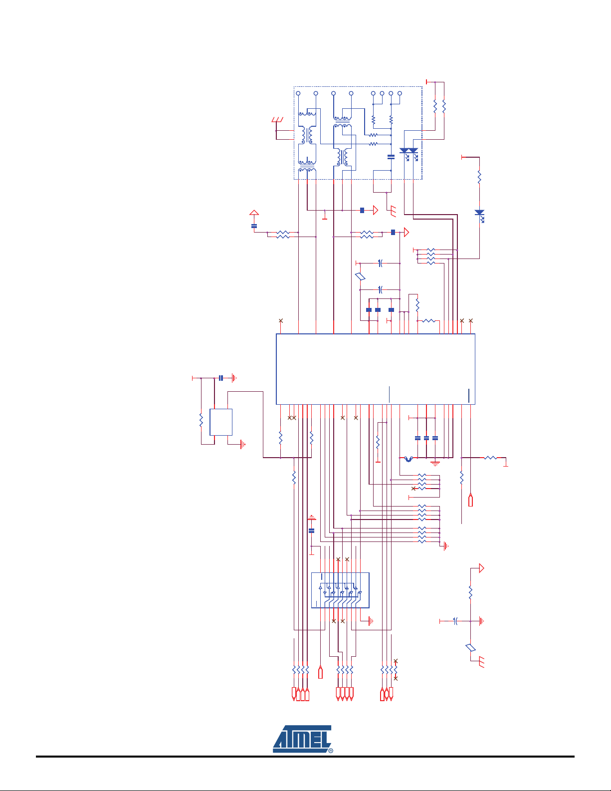
Figure 4-26. ETH1 Port
Evaluation Kit Hardware
1
2
3
6
457
TX+
TX-
RX+
RX-
75
EAR TH_E TH1
169
15
75
7575
1nF
ETH1
RJ45 ETHERNET CONNECTOR
GND_ETH1
C89
100n
(Only availabel for SAM9X25)
C88
100n
VDDIOP1
41
32
VDD
50MHz
VSS OUT
OE
Y2
R120 10k
R124
R123
43
XT1
REF_CLK/XT2
MN13
42
TD+
J18
J0026D21B
1
49.9R
49.9R
7
TX+
TXD317TXD218TXD020TXD119TX_CLK/ISOLATE22RXD0/PHYAD029RXD1/PHYAD128RXD2/PHYAD227RXD3/PHYAD3
TX_EN
21
TD-CTRD+
2
E1_AVDDT
8
TX-
26
7
3
RX+
RD-
CT
836
4
RX_CLK/10BTSER34RX_DV/TESTMODE37RX_ER/RXD4/RPTR
C91
100n
R127
49.9R
R126
49.9R
E1_AVDDT
L11
2200R
1 2
C90 100n
RX-
AVDDR1AVDDR
TX_ER/ TXD416COL/RMII36MDC
38
4
GND_ETH1
C94
C93
C92 100n
2
CRS/PHYAD435MDI O25MDI NTR
24
5
C96
100n
10u
10V
10u
10V
C95 100n
E1_AVDDT
9
AVDDT
DM9161AEP
32
VDDIOP1
8
Left LED
Right LED
111210
EARTH_ETH1
GND_ETH1
6
VDDIOP1
7
8
R130
R129 0R
6
46
47
AGND5AGND
AGND
BGRESG
DVDD
DISMDIX39DVDD30DVDD
41
VDDIOP1
R131 470R
R132 470R
VDDIOP1
470R
R169
12
D8 Red
RR16
10k
4 5
3
2
1
6.8k
31
11
48
BGRES
LEDMODE
15
23
FULL DU PLEX
45
14
N.C
LED2/OP213LED1/OP112LED0/OP0
CABLESTS/LINKSTS
DGND44DGND
PWRD WN10DGND33RESET
40
R122 0R
22R
R125 0R DNP
E1_RX0
E1_TX0
E1_TXEN
C114 100n
MN17
678
4 5
PC18
PC27
PC19
E1_RX1
SELCONFI G
E1_TXCK
VDDIOP1
O0I4O1I5O2I6O3
VCC
OE2
OE1I0O4I1O5I2O6I3O7
123456789
E1_RX0
E1_RX1
SELCONFI G
RR10
22R
123
SELCONFI G
E1_CRSDV
E1_CRSDV
678
PC21
PC20
R121 0R
E1_TXCK
E1_TX1
E1_TXCK
RR11
123
PC29
R128 1.5k
VDDIOP1
E1_RXER
E1_INTR
121314151617181920
E1_RXER
4 5
PC28
PC16
E1_MDIO
E1_MDC
I7
GND
74AC244SC
10 11
RR12
22R
123
PC30
C97 100n
C98 100n
C99 100n
1 2
JP13
4 5
3
6
7
8
VDDIOP1
6
7
8
6
7
8
E1_INTR
E1_INTR
678
4 5
PC31
PC26
RR15
10k
2
1
4 5
3
RR14
10k
2
1
4 5
3
RR13
10k
2
1
VDDIOP1
R134
47k
R133 0R
NRST
SELCONFI G
R136 0R
C100
10u
10V
1 2
L20
220ohm at 100MHz
VDDIOP1
GND_ETH1
EARTH_ETH1
Evaluation Kit (EK) User Guide 4-33
11115A–ATARM–27-Jul-11
Page 45
Evaluation Kit Hardware
4.3.3.8 Audio
The Evaluation Kit includes a WM8731 CODEC for digital sound input and output. This interface
includes audio jacks for line audio input (J13) and headphone line output (J15).
The SAM9 processor is configured in IIS slave mode to interface with the WM8731 Codec. The IIS master mode is also possible for evaluation by populating R162/R164 and removing the crystal Y3.
Figure 4-27. Audio Interface
VDDIOP0
R79
R77
CSB = 1:
addr=0011011
R76
R75
MODE = 0: 2-wire
MPU mode for 9x5
TWI interface
PA31
PA30
C117
PA27
PA24
PA26
PA25
PA29
PA28
4.7k
4.7k
C40 10u
C46 10u
22
CSB
TWI_addr
C45 100n
TWC K0
TWD 0
VDDIOP0
27
12324
SDIN
SCLK
DBVDD
DCVDD
10k
10k
21
MODE
C47 100n
AUDI O_GND
C48 10u
C51 10u
C50 100n
VCC_D AC
14
8
AVDD
HPVDD
AUDI O_GND
RK
C53 100n
C56 100n
C54 10u
R86 0R
164357
VMIDMICIN
TKTDTF
R87 33R
DACDAT
BCLK
RF
RD
R88 0R
R89 0R
in Slave Mode
IIS of Audio Interface
6
ADCLRC
ADCD AT
DACLRC
DGND
VCC_D AC
L18
VDDIOP0
28
100n
AUDI O_GND
1 2
220ohm at 100MHz
R165 0R
C116
100n
C115
10u
Y3
12.288MHz
C122
22p
24
1 3
C121
22p
DNP
R162 0R
R162 near CODEC
R164 near SODIMM
R164
22R DNP
PCK0
PB10
11
OSC
15
LLINEIN
LOUT
34
C44
C41
470p
470p
ROUT
13
12
470p
470p
5.6K
5.6K
AUDI O_GND
AUDI O_GND
CLKOUT
XTI/M CLK
MN1 0 W M8731SEDS
R74
5.6K
R78
1 2
L3
220ohm at 100MHz
L4
25
XTO
2
25
26
R81
R80
5.6K
C43
1 2
220ohm at 100MHz
1
C42
RLINEIN
MICBIAS
RHPOUT
18
C55 100n
10
17
AUDI O_GND
19
20
C49 1u
C52 1u
AUDI O_GND
AUDIO_GND
AGND HPGND
LHPOU T
9
+
C59 220uF /10V+C60 220uF /10V
L6
220ohm at 100MHz
1 2
25
AUDIO_GND
R91
47k
R90
L7
220ohm at 100MHz
1 2
1
34
AUDIO_GND
47k
C62
470p
AUDIO_GND
C61
470p
AUDI O_GND
J13
LINE_IN
STEREO_3.5mm
HEADPHONE
J15
STEREO_3.5mm
4-34 Evaluation Kit (EK) User Guide
11115A–ATARM–27-Jul-11
Page 46

4.3.3.9 1-Wire EEPROM
The EK board also features a 1-Wire device acting as a “firmware label” to store information like chip
type, manufacturer’s name, production date etc.
Figure 4-28. 1-Wire on EK
4.3.3.10 CAN Bus
Two boards, the SAM9X35-EK and SAM9X25-EK, feature two Controller Area Network (CAN) ports with
transceiver.
PB18
ONE_WIRE
R145 0R
VDDAN A
R144
1.5k
MN1 6
2
1
DS2431P
I/O
GND
Evaluation Kit Hardware
3
NC1
4
NC2
5
NC3
6
NC4
CAN0 uses the same IOs (PA9, PA10) as the DBGU. A jumper, JP11, is used to select either of the
interfaces.
Open JP11 to select the CAN function.
Close JP11 to select the DBGU function.
A 3-state output buffer, MN19 is inserted in series with the output channels of the CAN transceiver,
which share IOs with the DBGU. This is necessary because the CAN transceiver does not feature
3-state outputs.
Figure 4-29. CAN on EK
(only for SAM9X35/SAM9X25)
R21 10k
Y
R20 0R
5
4
R32 10k
R33 0R
R35 10k
R37 0R
PA10
SEL_CAN
PA9
CANTX0
CANRX0
PA5
PA6
MN1 9
1
OE
VCC
2
A
3
GND
SN74LVC1G126D BV
CANTX1
VDDI OP0
CANRX1
VDDI OP0
MN5
8
RS
CANH
1
D
CANL
5
EN
4
R
GND
SN65HVD234DR
MN6
8
RS
CANH
1
D
CANL
5
EN
4
R
GND
SN65HVD234DR
VCC
VCC
JP7
1 2
C20
100n
1 2
C23
100n
SIP2
JP8
SIP2
7
6
3
2
7
6
3
2
VDDI OP0
VDDI OP0
C24
10u
C21
10u
R19
120R
R34
120R
3V3
5V
3V3
5V
CON2
1
2
3
4
5
6
MJM0606GE06-H
CON3
1
2
3
4
5
6
MJM0606GE06-H
CAN0
CAN1
Evaluation Kit (EK) User Guide 4-35
11115A–ATARM–27-Jul-11
Page 47

Evaluation Kit Hardware
4.3.3.11 Telephone Interface
The Evaluation Kit features a smart DAA (Data Access Arrangement) chip to drive an analog telephone
line on RJ11 6P4C port (J16).
Figure 4-30. Telephone Interface
RJ11
12345
J16
1 2
L8
220ohm at 100MHz
3
0805
R92 6.81M
MN11
MJM0606GE06-H
6
D4
TB3100M-13-F
C63
470p12C64
470p
12
1 2
L9
220ohm at 100MHz
2
2
MMBD3004S-7-FD3
3
MMBD3004S-7-FD5
1
1
DAA_GND
0805
R93 6.81M
C67 100n
5
TAC
PWR15AVDD
11
EIC
2
4
RAC
TEST
12
100V
1%
R98
280R
1206
1%
R97
280R
1206 1206
1%1%
R96
280R
R95
280R
1206
MMBAT42
Q5
2 3
R101
3.01R
1
Q4
1
C69
10n
DAA_GND
MMBAT42
Q2
2 3
1
C68 47n
DAA_GND
R94
237K
6
RXI
DIBN
16
1
Q3
R99 100R
10
7
8
9
EIF
EIO
TXF
TXO
DIBP
14
1%
R103
9R1
1%
MMBAT42
2 3
R100
3.01R
1%
2 3
R102
MMBAT42
1
110R
13
CX20548-11Z
GPIO
EP
17
VC
3
DVDD
1206
DAA_GND
DAA_GND
C74
100n
DAA_GND
C66
100n
DAA_GND
C65
100n
TX1
0R can be replaced by
bead to improve EMI
DVDD
C70
47pF
4
LAN0066-50
1
2 3
C72
150pF
C71
150pF
R166 0R
R167 0R
DIBP
DIBN
DAA_GND
C73
100n
4-36 Evaluation Kit (EK) User Guide
11115A–ATARM–27-Jul-11
Page 48

4.3.3.12 SD/MMC Interface
The Evaluation Kit has two high-speed MultiMedia Card Interfaces (MCI). The first interface is used as a
4-bit interface (MCI0), connected to a MicroSD card slot. The second interface is used as a 4-bit interface (MCI1), connected to an SD/MMC card slot.
The memory card is not included in the Evaluation Kit.
Please note that the power is connected to VCC, which is 3.3 volts.
Figure 4-31. SD/MMC Interface
PD15
PA18
PA15
PA17
PA16
PA20
PA19
(MCI0_CD)
(MCI0_DA1)
(MCI0_DA0)
(MCI0_CK)
(MCI0_CDA)
(MCI0_DA3)
(MCI0_DA2)
VDDNF VDDI OP0
R10
R12
R11
68k
68k
R13
68k
R14
10k
R9
10k
RR1 27R
1
2
3
4 5
1
2
3
4 5
RR2 27R
68k
8
7
6
8
7
6
C11
100n
Evaluation Kit Hardware
Micro SD
J6
10
SW2
8
7
6
5
4
3
2
1
SW1
PJS008-2110-0
9
11
12
13
14
PD14
PA2
PA11
PA13
PA12
PA4
PA3
JP6
1 2
SIP2
(MCI1_WP)
(MCI1_CD)
(MCI1_DA1)
(MCI1_DA0)
(MCI1_CK)
(MCI1_CDA)
(MCI1_DA3)
(MCI1_DA2)
RR427R
1
2
3
4 5
1
2
3
4 5
VDDI OP0 VDD NF
R15
R16
R17
R18
68k
68k
68k
68k
8
7
6
8
RR5
7
27R
6
123
3V3
678
RR3
10k
4 5
J7
8
DAT1
7
DAT0
6
VSS
C12
100n
5
CLK
4
VDD
3
VSS
2
CMD
1
DAT3
9
DAT2
7SDCN-B0-0101-F
GND
GND
SH
SH
10
CD
11
WP
12
13
14
15
Evaluation Kit (EK) User Guide 4-37
11115A–ATARM–27-Jul-11
Page 49

Evaluation Kit Hardware
4.3.3.13 ZigBee
The EK board has a 10-pin male connector for the Atmel RZ600 ZigBee module.
DNP 0 Ohm resistors have been implemented in series with the PIO lines that are used elsewhere in the
design. Thereby, enable their individual disconnections, should a conflict occur in user application.
Figure 4-32. ZigBee Interface
4.3.3.14 LED Indicators
The EK board has three LED indicators for purposes shown below:
ZB_RSTN
PA13
PA0
PA21
PD16
ZB_IRQ1
SPI1_NPCS1
SPI1_MISO
DNP
DNP
DNP
DNP
R52 0R
R56 0R
R55 0R
R82 0R
J10
1 2
3 4
5 6
7 8
9 10
HD2X05
DNP
DNP
R53 0R
R57 0R
C25
15p
C26
2.2n
ZB_IRQ0
PD17
SPI1_MOSI
SPI1_SPCK
JP10
C27
DNP
2.2u
12
DNP
3V3
PA7
ZB_SLPTR
PA22
PA23
Table 4-8. LED Indicators
Reference Color Function
D2 Red 3v3 Power indicator
D7 Red ETH0 Full Duplex
D8 Red ETH1 Full Duplex
Refer to Section 4.3.3.2 ”Power Supplies” and Section 4.3.3.7 ”Ethernet 10/100 (EMAC) Port” for
details.
4.3.3.15 Expansion Ports
Most GPIOs are routed to expansion ports J1, J2, J3.
All I/Os of the MPU Image Sensor Interface (ISI) are routed to connectors J21.
The LCD and touch screen interfaces are routed to connectors J21, J22.
Figure 4-33. I/O Expansion
PA0
PA1
PA2
PA3
PA4
PA5
PA6
PA7
PA8
PA9
PA10
PA11
PA12
PA13
PA14
PA15
3V3
JP1
1
2
J1
HD2X20-HH
1 2
3 4
5 6
7 8
9 10
11 12
13 14
15 16
17 18
19 20
21 22
23 24
25 26
27 28
29 30
31 32
33 34
35 36
37 38
39 40
5V3V3
3
PA16
PA17
PA18
PA19
PA20
PA21
PA22
PA23
PA24
PA25
PA26
PA27
PA28
PA29
PA30
PA31
3V3
3V3 3V3
3V3 5V
JP2
1
J2
HD2X20-HH
1 2
3 4
5 6
PC0
7 8
PC1
9 10
PC2
11 12
PC3
13 14
PC4
15 16
PC5
17 18
PC6
19 20
PC7
21 22
PC8
23 24
PC9
25 26
PC10
27 28
PC11
29 30
PC12
31 32
PC13
33 34
PC14
35 36
PC15
37 38
39 40
5V3V3
3
2
PC16
PC17
PC18
PC19
PC20
PC21
PC22
PC23
PC24
PC25
PC26
PC27
PC28
PC29
PC30
PC31
3V3
JP3
1
1 2
3 4
5 6
PB0
7 8
PB1
9 10
PB2
11 12
PB3
13 14
PB4
15 16
PB5
17 18
PB6
19 20
PB7
21 22
PB8
23 24
PB9
25 26
PB10 PD16
27 28
PB11
29 30
PB12
31 32
PB13
33 34
PB14
35 36
PB15
37 38
39 40
2
J3
HD2X20-HH
3
PB16
PB17
PB18
PD14
PD15
PD17
PD18
PD19
PD20
PD21
3V3
4-38 Evaluation Kit (EK) User Guide
11115A–ATARM–27-Jul-11
Page 50

Figure 4-34. LCD and ISI Expansion
3V3_LCD
R5 0R DNP
R6 0R DNP
CHAN GE#
ZB_IRQ0
TWC K0 TWD 0
LCDD AT1
LCDD AT3
LCDD AT5
LCDD AT7
LCDD AT9
LCDD AT11
3V3
1 2
3 4
5 6
7 8
9 10
11 12
13
15
17
19
21 22
23 24
25 26
27 28
29 30
J2
14
16
18
20
TSM-115-01-L-DV-A
LCDDAT15
LCDDAT13
LCDDAT14
LCDDAT12
LCDDAT0
LCDDAT2
LCDDAT4
LCDDAT6
LCDDAT8
LCDDAT10
Evaluation Kit Hardware
4.3.4 Configuration
This section describes the PIO usage, the jumpers, the test points and the solder drops of the EK board.
4.3.4.1 JTAG/ICE Configuration
Table 4-9. JTAG/ICE
Designation Default Setting Feature
SELCONF IG
LCDD AT16
LCDD AT18
LCDD AT20
LCDD AT22
LCDD ISP
LCDVSY NC
LCDD EN
AD0_XP
AD2_Y P
AD4_LR
R22 0R
5V_INTER
J3
1 2
3 4
5 6
7 8
9 10
11 12
13
15
17
19
21 22
23 24
25 26
27 28
29 30
31 32
33 34
35 36
37 38
39 40
TSM-120-01-L-DV-A
14
16
18
20
LCDDAT17
LCDDAT19
LCDDAT21
LCDDAT23
LCDPW M
LCDHSYNC
LCDPC K
AD1_XM
AD3_Y M
R19 0R
LCD_D ETEC T
ONE_WI RE
R23 0R
R50 Not Populated Disables the ICE NTRST input
R51 Populated
Enables the ICE RTCK return. R94 must
be opened
R54 Populated Enables the ICE NRST input
R58 Not Populated Disables TCK <-> RTCK local loop
4.3.4.2 Boot Mode Select Configuration
Table 4-10. BMS
Designation Default Setting Feature
JP9 Open
Evaluation Kit (EK) User Guide 4-39
Default to boot on embedded ROM
Close to boot on external memory
11115A–ATARM–27-Jul-11
Page 51
Evaluation Kit Hardware
4.3.4.3 Force Power ON Configuration
Table 4-11. Force Power ON
Designation Default Setting Feature
JP5 Close
4.3.4.4 White Protection Configuration on MCI1
Table 4-12. Write Protection on MCI1
Designation Default Setting Feature
JP6 Close
4.3.4.5 Selection between DBGU and CAN
Table 4-13. Select DBGU or CAN
Designation Default Setting Feature
JP11 Close
4.3.4.6 Codec IIS Configuration
Keep on-board regulator always on
Open to feature SHDN function
MCI1 write protect selected
Open to disable protection
Default to select DBGU
Open to select CAN0
Table 4-14. Codec IIS
Designation Default Setting Feature
R162, R164 Not Populated IIS master mode, clock the codec by PCK0
C121, C122, Y3 Populated
4.3.4.7 ETH0 Configuration
Table 4-15. ETH0
Designation Default Setting Feature
R180, R183, R184,
R185, R185, R186,
R174, R175, R176
R177, R178, R179,
R181, R182, R218,
R171, R172, R173
IIS slaver mode, clock the codec by
external crystal
Populated to select the PHY channel on
Not Populated
Populated Selection of PHY channel on EK
CM. Channel on EK must be cut if select
the PHY on CM.
4-40 Evaluation Kit (EK) User Guide
11115A–ATARM–27-Jul-11
Page 52

Evaluation Kit Hardware
4.3.4.8 PIO Usage
Table 4-16. PIO A Pin Assignment and Signal Description
Signal Alternate Periph A Periph B Periph C
PA0 TXD0 SPI1_NPCS1 TXD0/ ZigBee USART0 shared with ZigBee
PA1 RXD0 SPI0_NPCS2 RXD0 USART0
PA2 RTS0 MCI1_DA1 E0_ETX0 RTS0/ MCI1 USART0 shared with MCI1
PA3 CTS0 MCI1_DA2 E0_ETX1 CTS0/ MCI1 USART0 shared with MCI1
PA4 SCK0 MCI1_DA3 E0_ETXER MCI1
PA5 TXD1 CANTX1 CAN1
PA6 RXD1 CANRX1 CAN1
PA7 TXD2 SPI0_NPCS1 ZB_IRQ0
PA8 RXD2 SPI1_NPCS0 DataFlash
PA9 CANRX0 DBGU+CAN0 DBGU shared with CAN0
PA10 CANTX0 DBGU+CAN0 DBGU shared with CAN0
PA11 SPI0_MISO MCI1_DA0 MCI1
PA12 SPI0_MOSI MCI1_CDA MCI1
PA13 SPI0_SPCK MCI1_CK MCI1 ZB_IRQ1
PA14 SPI0_NPCS0 MCI0
PA15 MCI0_DA0 MCI0
PA16 MCI0_CDA MCI0
PA17 MCI0_CK MCI0
PA18 MCI0_DA1 MCI0
PA19 MCI0_DA2 MCI0
PA20 MCI0_DA3 DataFlash
PA21 TIOA0 SPI1_MISO ZigBee DataFlash
PA22 TIOA1 SPI1_MOSI ZigBee DataFlash
PA23 TIOA2 SPI1_SPCK ZigBee SSC
PA24 TCLK0 TK SSC
PA25 TCLK1 TF SSC
PA26 TCLK2 TD SSC
PA27 TIOB0 RD SSC
PA28 TIOB1 RK SSC
PA29 TIOB2 RF SSC
PA30 TWD0 SPI1_NPCS3 E0_EMDC TWD0
PA31 TWCK0 SPI1_NPCS2 E0_ETXEN TWCK0
Evaluation Kit (EK) User Guide 4-41
11115A–ATARM–27-Jul-11
Page 53

Evaluation Kit Hardware
Table 4-17. PIO B Pin Assignment and Signal Description
Signal Alternate Periph A Periph B Periph C Module CM EK
PB0 E0_RX0 RTS2 ETH0
PB1 E0_RX1 CTS2 ETH0
PB2 E0_RXER SCK2 ETH0
PB3 E0_RXDV SPI0_NPCS3 ETH0
PB4 E0_TXCK TWD2 ETH0
PB5 E0_MDIO TWCK2 ETH0
PB6 AD7 E0_MDC ETH0
PB7 AD8 E0_TXEN ETH0
PB8 AD9 E0_TXER ETH0_INTR
PB9 AD10 E0_TX0 PCK1 ETH0
PB10 AD11 E0_TX1 PCK0 ETH0
PB11 AD0xp E0_TX2 PWM0 TSC
PB12 AD1xm E0_TX3 PWM1 TSC
PB13 AD2yp E0_RX2 PWM2 TSC
PB14 AD3ym E0_RX3 PWM3 TSC
PB15 AD4lr E0_RXCK TSC
PB16 AD5 E0_CRS VBUS_SENSE (USB)
PB17 AD6 E0_COL OVCUR_USB (Open drain)
PB18 IRQ ADTRG USER_LED1# ONE_WIRE
4-42 Evaluation Kit (EK) User Guide
11115A–ATARM–27-Jul-11
Page 54

Evaluation Kit Hardware
Table 4-18. PIO C Pin Assignment and Signal Description
Signal Alternate Periph A Periph B Periph C EK f (LCD) EK f (ISI+IO)
PC0 LCDDAT0 ISI_D0 TWD1 LCDDAT0 ISI_D0
PC1 LCDDAT1 ISI_D1 TWCK1 LCDDAT1 ISI_D1
PC2 LCDDAT2 ISI_D2 TIOA3 LCDDAT2 ISI_D2
PC3 LCDDAT3 ISI_D3 TIOB3 LCDDAT3 ISI_D3
PC4 LCDDAT4 ISI_D4 TCLK3 LCDDAT4 ISI_D4
PC5 LCDDAT5 ISI_D5 TIOA4 LCDDAT5 ISI_D5
PC6 LCDDAT6 ISI_D6 TIOB4 LCDDAT6 ISI_D6
PC7 LCDDAT7 ISI_D7 TCLK4 LCDDAT7 ISI_D7
PC8 LCDDAT8 ISI_D8 UTXD0 LCDDAT8 ISI_D8
PC9 LCDDAT9 ISI_D9 URXD0 LCDDAT9 ISI_D9
PC10 LCDDAT10 ISI_D10 PWM0 LCDDAT10 ISI_D10
PC11 LCDDAT11 ISI_D11 PWM1 LCDDAT11 ISI_D11
PC12 LCDDAT12 ISI_PCK TIOA5 LCDDAT12 ISI_PCK
PC13 LCDDAT13 ISI_VSYNC TIOB5 LCDDAT13 ISI_VSYNC
PC14 LCDDAT14 ISI_HSYNC TCLK5 LCDDAT14 ISI_HSYNC
PC15 LCDDAT15 ISI_MCK PCK0 SSC LCDDAT15 ISI_MCK/PCK0
PC16 LCDDAT16 E1_RXER UTXD1 LCDDAT16 E1_RXER
PC17 LCDDAT17 URXD1 LCDDAT17
PC18 LCDDAT18 E1_TX0 PWM0 LCDDAT18 E1_TX0
PC19 LCDDAT19 E1_TX1 PWM1 LCDDAT19 E1_TX1
PC20 LCDDAT20 E1_RX0 PWM2 LCDDAT20 E1_RX0
PC21 LCDDAT21 E1_RX1 PWM3 LCDDAT21 E1_RX1
PC22 LCDDAT22 TXD3 LCDDAT22 TXD3
PC23 LCDDAT23 RXD3 LCDDAT23 RXD3
PC24 LCDDISP RTS3 LCDDISP RTS3
PC25 CTS3 CTS3
PC26 LCDPWM SCK3 Eth1_Intr1 LCDPWM
PC27 LCDVSYNC E1_TXEN RTS1 LCDVSYNC E1_TXEN
PC28 LCDHSYNC E1_CRSDV CTS1 LCDHSYNC E1_CRSDV
PC29 LCDDEN E1_TXCK SCK1 LCDDEN E1_TXCK
PC30 LCDPCK E1_MDC LCDPCK E1_MDC
PC31 FIQ E1_MDIO PCK1 E1_MDIO
Evaluation Kit (EK) User Guide 4-43
11115A–ATARM–27-Jul-11
Page 55

Evaluation Kit Hardware
Table 4-19. PIO D Pin Assignment and Signal Description
Signal Alternate Periph A Periph B Periph C Module CM EK
PD0 NANDOE Nand Flash
PD1 NANDWE Nand Flash
PD2 A21/NANDALE Nand Flash
PD3 A22/NANDCLE Nand Flash
PD4 NCS3 CS NAND Flash
PD5 NWAIT NAND_RD/BY
PD6 D16 Nand Flash
PD7 D17 Nand Flash
PD8 D18 Nand Flash
PD9 D19 Nand Flash
PD10 D20 Nand Flash MCI0_CD (switch)
PD11 D21 Nand Flash MCI1_CD (switch)
PD12 D22 Nand Flash ZB_RSTN
PD13 D23 Nand Flash ZB_SLPTR
PD14 D24 EN5V_HDA#
PD15 D25 A20 EN5V_HDB#
PD16 D26 A23 EN5V_HDC#
PD17 D27 A24
PD18 D28 A25
PD19 D29 NCS2
PD20 D30 NCS4
PD21 D31 NCS5 POWR_LED
4-44 Evaluation Kit (EK) User Guide
11115A–ATARM–27-Jul-11
Page 56

4.3.5 Connectors
4.3.5.1 Power Supply
Figure 4-35. Power Supply Connector J4
Table 4-20. Power Supply Connector J2 Signal Description
Evaluation Kit Hardware
Pin Mnemonic Signal description
1 Center +5V
2 GND
3 Floating
4.3.5.2 SODIMM Card Edge Socket
The Evaluation Kit uses a SODIMM200 standard connector for CM board interfacing.
Please note that this is not an industry standard pin-out and that it is unlikely to be compatible with offthe-shelf SODIMM cards.
Figure 4-36. SODIMM200 Socket CON1
Table 4-21. SODIMM200 CON1 Signal Descriptions
Function Type x5 pad name SODIMM 200 x5 pad name Type Function
Front Side A B Back Side
VCC 3V3 POWER OUTPUT 1 2 POWER OUTPUT VCC 3V3
VCC 3V3 POWER OUTPUT 3 4 POWER OUTPUT VCC 3V3
GND 5 6 POWER OUTPUT VBAT
USBC_DP I/O USB Data Positive 7 8 SYSC JTAGSEL
USBC_DM I/O USB Data Negative 9 10 SYSC WKUP
GND 11 12 SYSC SHDN
Evaluation Kit (EK) User Guide 4-45
11115A–ATARM–27-Jul-11
Page 57

Evaluation Kit Hardware
Table 4-21. SODIMM200 CON1 Signal Descriptions (Continued)
Function Type x5 pad name SODIMM 200 x5 pad name Type Function
USBB_DM I/O USB Data Negative 13 14 SYSC BMS
USBB_DP I/O USB Data Positive 15 16 SYSC nRST
GND 17 18 SYSC nTRST
DIBP I/O 19 20 RSTJTAG TDI
DIBN I/O 21 22 RSTJTAG TCK
GND 23 24 RSTJTAG TMS
USBA_DM I/O USB Data Negative 25 26 RSTJTAG TDO
USBA_DP I/O USB Data Positive 27 28 RSTJTAG RTCK
GND 29 30 PWR_EN
RFU RFU 31 32 RFU RFU
RFU RFU 33 34 RFU RFU
RFU RFU 35 36 RFU RFU
RFU RFU 37 38 RFU RFU
RFU RFU 39 40 RFU RFU
KEY
GND 41 42 GND
RFU RFU 43 44 RFU RFU
RFU RFU 45 46 RFU RFU
RFU RFU 47 48 RFU RFU
RFU RFU 49 50 RFU RFU
GND 51 52 GND
RFU RFU 53 54 RFU RFU
RFU RFU 55 56 RFU RFU
RFU RFU 57 58 RFU RFU
RFU RFU 59 60 RFU RFU
VDDNF POWER DOMAIN FROM CM 61 62 POWER DOMAIN FROM CM VDDNF
PD0 GPIO D NANDOE 63 64 NANDWE GPIO D PD1
PD2 GPIO D A21/NANDALE 65 66 A22/NANDCLE GPIO D PD3
PD4 GPIO D NCS3 67 68 NWAIT GPIO D PD5
PD6 GPIO D D16 69 70 D17 GPIO D PD7
PD8 GPIO D D18 71 72 D19 GPIO D PD9
GND 73 74 GND
PD10 GPIO D D20 75 76 D21 GPIO D PD11
PD12 GPIO D D22 77 78 D23 GPIO D PD13
PD14 GPIO D D24 79 80 D25/A20 GPIO D PD15
PD16 GPIO D D26/A23 81 82 D27/A24 GPIO D PD17
PD18 GPIO D D28/A25 83 84 D29/NCS2 GPIO D PD19
4-46 Evaluation Kit (EK) User Guide
11115A–ATARM–27-Jul-11
Page 58

Evaluation Kit Hardware
Table 4-21. SODIMM200 CON1 Signal Descriptions (Continued)
Function Type x5 pad name SODIMM 200 x5 pad name Type Function
USBB_DM I/O USB Data Negative 13 14 SYSC BMS
USBB_DP I/O USB Data Positive 15 16 SYSC nRST
GND 17 18 SYSC nTRST
DIBP I/O 19 20 RSTJTAG TDI
DIBN I/O 21 22 RSTJTAG TCK
GND 23 24 RSTJTAG TMS
USBA_DM I/O USB Data Negative 25 26 RSTJTAG TDO
USBA_DP I/O USB Data Positive 27 28 RSTJTAG RTCK
GND 29 30 PWR_EN
RFU RFU 31 32 RFU RFU
RFU RFU 33 34 RFU RFU
RFU RFU 35 36 RFU RFU
RFU RFU 37 38 RFU RFU
RFU RFU 39 40 RFU RFU
KEY
GND 41 42 GND
RFU RFU 43 44 RFU RFU
RFU RFU 45 46 RFU RFU
RFU RFU 47 48 RFU RFU
RFU RFU 49 50 RFU RFU
GND 51 52 GND
RFU RFU 53 54 RFU RFU
RFU RFU 55 56 RFU RFU
RFU RFU 57 58 RFU RFU
RFU RFU 59 60 RFU RFU
VDDNF POWER DOMAIN FROM CM 61 62 POWER DOMAIN FROM CM VDDNF
PD0 GPIO D NANDOE 63 64 NANDWE GPIO D PD1
PD2 GPIO D A21/NANDALE 65 66 A22/NANDCLE GPIO D PD3
PD4 GPIO D NCS3 67 68 NWAIT GPIO D PD5
PD6 GPIO D D16 69 70 D17 GPIO D PD7
PD8 GPIO D D18 71 72 D19 GPIO D PD9
GND 73 74 GND
PD10 GPIO D D20 75 76 D21 GPIO D PD11
PD12 GPIO D D22 77 78 D23 GPIO D PD13
PD14 GPIO D D24 79 80 D25/A20 GPIO D PD15
PD16 GPIO D D26/A23 81 82 D27/A24 GPIO D PD17
PD18 GPIO D D28/A25 83 84 D29/NCS2 GPIO D PD19
Evaluation Kit (EK) User Guide 4-47
11115A–ATARM–27-Jul-11
Page 59

Evaluation Kit Hardware
Table 4-21. SODIMM200 CON1 Signal Descriptions (Continued)
Function Type x5 pad name SODIMM 200 x5 pad name Type Function
USBB_DM I/O USB Data Negative 13 14 SYSC BMS
USBB_DP I/O USB Data Positive 15 16 SYSC nRST
GND 17 18 SYSC nTRST
DIBP I/O 19 20 RSTJTAG TDI
DIBN I/O 21 22 RSTJTAG TCK
GND 23 24 RSTJTAG TMS
USBA_DM I/O USB Data Negative 25 26 RSTJTAG TDO
USBA_DP I/O USB Data Positive 27 28 RSTJTAG RTCK
GND 29 30 PWR_EN
RFU RFU 31 32 RFU RFU
RFU RFU 33 34 RFU RFU
RFU RFU 35 36 RFU RFU
RFU RFU 37 38 RFU RFU
RFU RFU 39 40 RFU RFU
KEY
GND 41 42 GND
RFU RFU 43 44 RFU RFU
RFU RFU 45 46 RFU RFU
RFU RFU 47 48 RFU RFU
RFU RFU 49 50 RFU RFU
GND 51 52 GND
RFU RFU 53 54 RFU RFU
RFU RFU 55 56 RFU RFU
RFU RFU 57 58 RFU RFU
RFU RFU 59 60 RFU RFU
VDDNF POWER DOMAIN FROM CM 61 62 POWER DOMAIN FROM CM VDDNF
PD0 GPIO D NANDOE 63 64 NANDWE GPIO D PD1
PD2 GPIO D A21/NANDALE 65 66 A22/NANDCLE GPIO D PD3
PD4 GPIO D NCS3 67 68 NWAIT GPIO D PD5
PD6 GPIO D D16 69 70 D17 GPIO D PD7
PD8 GPIO D D18 71 72 D19 GPIO D PD9
GND 73 74 GND
PD10 GPIO D D20 75 76 D21 GPIO D PD11
PD12 GPIO D D22 77 78 D23 GPIO D PD13
PD14 GPIO D D24 79 80 D25/A20 GPIO D PD15
PD16 GPIO D D26/A23 81 82 D27/A24 GPIO D PD17
PD18 GPIO D D28/A25 83 84 D29/NCS2 GPIO D PD19
4-48 Evaluation Kit (EK) User Guide
11115A–ATARM–27-Jul-11
Page 60

Evaluation Kit Hardware
Table 4-21. SODIMM200 CON1 Signal Descriptions (Continued)
Function Type x5 pad name SODIMM 200 x5 pad name Type Function
PD20 GPIO D D30/NCS4 85 86 D31/NCS5 GPIO D PD21
VDDIOP0 POWER OUTPUT 87 88 POWER OUTPUT VDDIOP0
PA0 GPIO A TXD0/SPI1-NPCS1 89 90 RXD0/SPI0-NPCS2 GPIO A PA1
PA2 GPIO A MCI1_DA1/E0_ETX0 91 92
PA4 GPIO A
PA11 GPIO A
PA13 GPIO A
GND 99 100
PA8 GPIO A RXD2/SPI1_NPCS0 101 102 TIOA0 /SPI1_MISO GPIO A PA21
PA22 GPIO A TIOA1/SPI1_MOS1 103 104
PA31 GPIO A
GND 107 108 MCI0_DA0 GPIO A PA15
PA16 GPIO A MCI0_CDA 109 110 MCI0_CK GPIO A PA17
PA18 GPIO A MCI0_DA1 111 112 MCI0_DA2 GPIO A PA19
PA20 GPIO A MCI0_DA3 113 114 GND
SCK0/MCI1_DA3/
E0_ETXER
SPI0_MISO/
MCI1_DA0
SPI0_SPCK/
MCI1_CK
TWCK0/SPI1_NPCS2/
E0_ETXEN
93 94 GND
95 96
97 98 SPI0_NPCS0 GPIO A PA14
105 106
CTS0/ MCI1_DA2/
E0_ETX1
SPI0_MOSI/
MCI1_CDA
TXD2/
SPI0_NPCS1
TIOA2/
SPI1_SPCK
TWD0/
SPI1_NPCS3/
E0_EMDC
GPIO A PA3
GPIO A PA12
GPIO A PA7
GPIO A PA23
GPIO A PA30
PA5 GPIO A TXD1/CANTX1 115 116 RXD1/CANRX1 GPIO A PA6
PA10 GPIO A DTXD/CANTX0 117 118 DRXD/CANRX0 GPIO A PA9
GND 119 120 TCLK0/TK GPIO A PA24
PA25 GPIO A TCLK1/TF 121 122 TCLK2/TD GPIO A PA26
PA27 GPIO A TIOB0/RD 123 124 TIOB1/RK GPIO A PA28
PA29 GPIO A TIOB2/RF 125 126 GND
VDDIOP1 POWER OUTPUT 127 128 POWER OUTPUT VDDIOP1
PC0 GPIO C LCDDAT0/ISI_D0 129 130 LCDDAT1 GPIO C PC1
PC2 GPIO C LCDDAT2/ISI_D2 131 132 LCDDAT3 GPIO C PC3
PC4 GPIO C LCDDAT4 133 134 LCDDAT5 GPIO C PC5
GND 135 136 LCDDAT6 GPIO C PC6
PC7 GPIO C LCDDAT7 137 138 LCDDAT8 GPIO C PC8
PC9 GPIO C LCDDAT9 139 140 LCDDAT10 GPIO C PC10
PC11 GPIO C LCDDAT11 141 142 GND
PC12 GPIO C LCDDAT12 143 144 LCDDAT13 GPIO C PC13
PC14 GPIO C LCDDAT14 145 146 LCDDAT15 GPIO C PC15
GND 147 148 LCDDAT16 GPIO C PC16
Evaluation Kit (EK) User Guide 4-49
11115A–ATARM–27-Jul-11
Page 61

Evaluation Kit Hardware
Table 4-21. SODIMM200 CON1 Signal Descriptions (Continued)
Function Type x5 pad name SODIMM 200 x5 pad name Type Function
PC17 GPIO C LCDDAT17 149 150 LCDDAT18 GPIO C PC18
PC19 GPIO C LCDDAT19 151 152 LCDDAT20 GPIO C PC20
PC21 GPIO C LCDDAT21 153 154 GND
PC22 GPIO C LCDDAT22 155 156 LCDDAT23 GPIO C PC23
PC24 GPIO C LCDDISP 157 158 GPIO C PC25
PC26 GPIO C LCDPWM 159 160 LCDVSYNC GPIO C PC27
GND 161 162 LCDHSYNC GPIO C PC28
PC29 GPIO C LCDDEN 163 164 E1_MDC GPIO C PC30
PC31 GPIO C E1_MDIO 165 166 SELCONFIG
VDDANA POWER OUTPUT 167 168 POWER OUTPUT VDDANA
PB0 GPIO B E0_RX0 169 170 E0_RX1 GPIO B PB1
PB2 GPIO B E0_RXER 171 172 E0_RXDV GPIO B PB3
PB4 GPIO B E0_TXCK 173 174 E0_MDIO GPIO B PB5
PB6 GPIO B E0_MDC 175 176 E0_TXEN GPIO B PB7
PB8 GPIO B E0_TXER 177 178 GNDANA
PB9 GPIO B E0_TX0 179 180 E0_TX1 GPIO B PB10
PB11 GPIO B E0_TX2 181 182 E0_TX3 GPIO B PB12
PB13 GPIO B E0_RX2 183 184 E0_RX3 GPIO B PB14
PB15 GPIO B E0_RXCK 185 186 E0_CRS GPIO B PB16
PB17 GPIO B E0_COL 187 188 GNDANA
PB18 GPIO B IRQ 189 190 POWER OUTPUT POWR_REF
GND 191 192 ETH LED0
ETH0_TX+ ETH 193 194 ETH LED1
ETH0_TX- ETH 195 196 ETH LED2
ETH0_RX+ ETH 197 198 ETH AVDDT
ETH0_RX- ETH 199 200 GND_ETH
4.3.5.3 JTAG/ICE Connector
Figure 4-37. JTAG J9
4-50 Evaluation Kit (EK) User Guide
11115A–ATARM–27-Jul-11
Page 62

Table 4-22. JTAG/ICE Connector J13 Signal Descriptions
Pin Mnemonic Description
This is the target reference voltage. It is used to check if the target has power,
1 VTref. 3.3V power
to create the logic-level reference for the input comparators, and to control the
output logic levels to the target. It is normally fed from VDD on the target board
and must not have a series resistor.
Evaluation Kit Hardware
2 Vsupply. 3.3V power
nTRST TARGET RESET - Active-low output
3
signal that resets the target
4 GND Common ground
TDI TEST DATA INPUT - Serial data output
5
line, sampled on the rising edge of the TCK
signal.
6 GND Common ground
7 TMS TEST MODE SELECT
8 GND Common ground
TCK TEST CLOCK - Output timing signal,
9
for synchronizing test logic and control
register access.
10 GND Common ground
RTCK - Input Return test clock signal from
11
the target.
This pin is not connected in SAM-ICE. It is reserved for compatibility with other
equipment. Connect to VDD or leave open in target system.
JTAG Reset. Output from SAM-ICE to the Reset signal on the target JTAG port.
Typically connected to nTRST on the target CPU. This pin is normally pulled
HIGH on the target to avoid unintentional resets when there is no connection.
JTAG data input of target CPU. It is recommended that this pin is pulled to a
defined state on the target board. Typically connected to TDI on target CPU.
JTAG mode set input of target CPU. This pin should be pulled up on the target.
Typically connected to TMS on target CPU. Output signal that sequences the
target's JTAG state machine, sampled on the rising edge of the TCK signal.
JTAG clock signal to target CPU. It is recommended that this pin is pulled to a
defined state on the target board. Typically connected to TCK on target CPU.
Some targets must synchronize the JTAG inputs to internal clocks. To assist in
meeting this requirement, a returned and retimed TCK can be used to
dynamically control the TCK rate. SAM-ICE supports adaptive clocking which
waits for TCK changes to be echoed correctly before making further changes.
Connect to RTCK if available, otherwise to GND.
12 GND Common ground
TDO JTAG TEST DATA OUTPUT - Serial
13
data input from the target.
14 GND Common ground
15 nSRST RESET Active-low reset signal. Target CPU reset signal.
16 GND Common ground
17 RFU This pin is not connected in SAM-ICE.
18 GND Common ground
19 RFU This pin is not connected in SAM-ICE.
20 GND Common ground
JTAG data output from target CPU. Typically connected to TDO on target CPU.
Evaluation Kit (EK) User Guide 4-51
11115A–ATARM–27-Jul-11
Page 63

Evaluation Kit Hardware
4.3.5.4 USB Type A Dual Port
Figure 4-38. USB Type A Dual Port J19
Table 4-23. USB Type A Dual Port J19 Signal Descriptions
Pin Mnemonic Description
A1 Vbus – USB_A 5V power
A2 DM – USB_A Data minus
A3 DP – USB_A Data plus
A4 GND Common ground
B1 Vbus – USB_A 5V power
B2 DM – USB_A Data minus
B3 DP – USB_A Data plus
B4 GND Common ground
Mechanical pins Shield
4-52 Evaluation Kit (EK) User Guide
11115A–ATARM–27-Jul-11
Page 64

4.3.5.5 USB Micro AB
Figure 4-39. USB USB Host/Device Micro AB Connector J20
Table 4-24. USB USB Host/Device Micro AB Connector J20 Signal Descriptions
Evaluation Kit Hardware
Pin Mnemonic Description
1 Vbus 5v power
2 DM Data minus
3 DP Data plus
4 ID On the Go Identification
5 GND Common ground
4.3.5.6 DBGU
Figure 4-40. DBGU Connector J11
Table 4-25. DBGU Connector J11 Signal Descriptions
Pin Mnemonic Description
1, 4, 6, 9 NO CONNECTION
2 RXD (RECEIVED DATA) RS232 serial data output signal
3 TXD (TRANSMITTED Data) RS232 serial data input signal
5 GND Common ground
7 RTS (REQUEST TO SEND) NO USED
8 CTS (CLEAR TO SEND) NO USED
Mechanical pins Shield
Evaluation Kit (EK) User Guide 4-53
11115A–ATARM–27-Jul-11
Page 65

Evaluation Kit Hardware
4.3.5.7 RS232 Connector with RTS/CTS Handshake Support
Figure 4-41. USART Connector J12, J13
Table 4-26. USART Connector J12 Signal Descriptions
Pin Mnemonic Description
1, 4, 6, 9 NO CONNECTION
2 RXD (RECEIVED DATA) PA1 RS232 serial data output signal
3 TXD (TRANSMITTED Data) PA0 RS232 serial data input signal
5 GND Common ground
7 RTS (REQUEST TO SEND) PA2 Active-positive RS232 input signal
8 CTS (CLEAR TO SEND) PA3 Active-positive RS232 output signal
Mechanical pins Shield
Table 4-27. USART Connector J13 Signal Descriptions
Pin Mnemonic Description
1, 4, 6, 9 NO CONNECTION
2 RXD (RECEIVED DATA) PC23 RS232 serial data output signal
3 TXD (TRANSMITTED Data) PC22 RS232 serial data input signal
5 GND Common ground
7 RTS (REQUEST TO SEND) PC24 Active-positive RS232 input signal
8 CTS (CLEAR TO SEND) PC25 Active-positive RS232 output signal
Mechanical pins Shield
4-54 Evaluation Kit (EK) User Guide
11115A–ATARM–27-Jul-11
Page 66

4.3.5.8 DAA RJ11 Socket (6P4C)
Figure 4-42. DAA RJ11 Socket J16
Table 4-28. DAA RJ11 Socket J16 Signal Descriptions
Pin Mnemonic Description
1, 2, 5, 6 NO CONNECTION
3 RAC RING side of ordinary telephone line
4 TAC TIP side of ordinary telephone line
4.3.5.9 CAN RJ12 Socket (6P6C)
Evaluation Kit Hardware
Figure 4-43. CAN RJ12 Socket CON2, CON3
Table 4-29. DAA RJ11 Socket J16 Signal Descriptions
Pin Mnemonic Description
1 3V3 POWER PIN
2 5V POWER PIN
4 CANL CAN bus differential pair
5 CANH CAN bus differential pair
4, 6 GND Common ground
Evaluation Kit (EK) User Guide 4-55
11115A–ATARM–27-Jul-11
Page 67

Evaluation Kit Hardware
4.3.5.10 MicroSD MCI0
Figure 4-44. MicroSD Socket J6
Table 4-30. MicroSD Socket J6 Signal Descriptions
Pin Mnemonic Description
1 DAT2 Data Bit 2
2 CD/DAT3 Card Detect/Data Bit 3
3 CMD Command Line
4 VCC Supply Voltage 3.3V
5 CLK Command Line
6 VSS Common ground
7 DAT0 Data Bit 0
8 DAT1 Data Bit 1
9 SW1 No use, grounded
10 CARD DETECT CARD DETECT
4.3.5.11 SD/MMC MCI1
Figure 4-45. SD/MMC Socket J7
Table 4-31. SD Socket J7 Signal Descriptions
Pin Mnemonic PIO
Signal
SD Card
MMC Card
1-Bit Mode 4-Bit Mode
1 MCI1_DA2 PA3 Not Used Read Wait (RW) Data Line DAT2 or Read Wait (RW)
2 MCI1_DA3 PA4 Reserved Not Used Data Line DAT3
3 MCI1_CDA PA12 Command/Response
4 VDDIOP0 Supply Voltage (3.3-volts) VDDIOP0
4-56 Evaluation Kit (EK) User Guide
11115A–ATARM–27-Jul-11
Page 68

Table 4-31. SD Socket J7 Signal Descriptions (Continued)
Evaluation Kit Hardware
Signal
Pin Mnemonic PIO
MMC Card
1-Bit Mode 4-Bit Mode
5 MCI1_CK PA13 Clock
6 GND Ground
7 MCI1_DA0 PA11 Data Line DAT0
8 MC1_DA1 PA2 Not Used Interrupt (IRQ) Data Line DAT1 or Interrupt (IRQ)
9 GND Ground
10 MCI1_CD PD14 Card Detect, configured as GPIO, Power domain VDDNF
11 WP Write Protect Detect, connects to jumper JP6
12 GND Ground
13 GND Ground
14 GND Ground
15 GND Ground
SD Card
4.3.5.12 Ethernet RJ45 Socket J17, J18
Figure 4-46. Ethernet RJ45 Socket J17, J18
Table 4-32. DAA RJ11 Socket J16 Signal Descriptions
Pin Mnemonic Description
1 TX+ DIFFERENTIAL OUTPUT PLUS
2 TX- DIFFERENTIAL OUTPUT MINUS
3 RX+ DIFFERENTIAL INPUT PLUS
4 Reserved
5 Reserved DIFFERENTIAL INPUT MINUS
6 RX-
7 Reserved
8 Reserved
Evaluation Kit (EK) User Guide 4-57
11115A–ATARM–27-Jul-11
Page 69

Evaluation Kit Hardware
4.3.5.13 ZigBee Socket J10
Figure 4-47. ZigBee Socket J10
Table 4-33. ZigBee Socket J10 Signal Descriptions
Function
Reset /RST 1 2 Misc.
Interrupt
Request
SPI chip select /SEL 5 6 MOSI SPI MOSI
SPI MISO MISO 7 8 SCLK SPI CLK
Power Supply GND GND 9 10 VCC VCC VCC
Signal
Name
IRQ 3 4 SLP_TR SLP_TR
Port Pin Pin Port
Signal
Name
Function
4.3.5.14 LCD/ISI Socket J21
Figure 4-48. LCD/ISI Socket J21
Option on misc. port set by
OR or solder shunts
EEprom for MAC
address, cap array
settings and serial
number
TST: test mode
activation
CLKM: RF chip clock
output
Voltage range: 1.8v to 5.5v,
regulated to 3.3v
Table 4-34. LCD/ISI Socket J21 Signal Descriptions
LCD ISI Pin Num Pin Num ISI LCD
3V3 3V3 1 2 GND GND
VDDISI VDDISI 3 4 GND GND
ZB_IRQ0 ZB_IRQ0 5 6 ZB_IRQ1
TWCK0 TWCK0 7 8 TWD0
GND GND 9 10 ISI_MCK LCDDAT15
GND GND 11 12 ISI_VSYNC LCDDAT13
GND GND 13 14 ISI_HSYNC LCDDAT14
4-58 Evaluation Kit (EK) User Guide
11115A–ATARM–27-Jul-11
Page 70

Table 4-34. LCD/ISI Socket J21 Signal Descriptions (Continued)
LCD ISI Pin Num Pin Num ISI LCD
GND GND 15 16 ISI_PCK LCDDAT12
GND GND 17 18 ISI_D0 LCDDAT0
LCDDAT1 ISI_D1 19 20 ISI_D2 LCDDAT2
LCDDAT3 ISI_D3 21 22 ISI_D4 LCDDAT4
LCDDAT5 ISI_D5 23 24 ISI_D6 LCDDAT6
LCDDAT7 ISI_D7 25 26 ISI_D8 LCDDAT8
LCDDAT9 ISI_D9 27 28 ISI_D10 LCDDAT10
LCDDAT11 ISI_D11 29 30 GND GND
4.3.5.15 LCD/TSC Socket J22
Figure 4-49. LCD/TSC Socket J22
Evaluation Kit Hardware
Table 4-35. LCD/TSC Socket J22 Signal Descriptions
LCD Pin Num Pin Num LCD
5V 5V_INTER 1 2 GND GND
5V 5V_INTER 3 4 GND GND
LCDDAT16 5 6 LCDDAT17
LCDDAT18 7 8 LCDDAT19
LCDDAT20 9 10 LCDDAT21
LCDDAT22 11 12 LCDDAT23
GND GND 13 14 GND GND
LCDDISP 15 16 LCDPWM
LCDCSYNC 17 18 LCDHSYNC
LCDDEN 19 20 LCDPCK
GND GND 21 22 GND GND
AD0_XP TSC 23 24 TSC AD1_XM
AD2_YP TSC 25 26 TSC AD3_YM
AD4_LR TSC 27 28 ONE_WIRE
GND GND 29 30 GND GND
SPI1_MISO 31 32 SPI1_MOSI
SPI1_SPCK 33 34 SPI1_NPCS1
EN_PWRLCD SELCONFIG 35 36 LCD_DETECT LCD_DETECT#
PD16 37 38 PD17
GND GND 39 40 GND GND
Evaluation Kit (EK) User Guide 4-59
11115A–ATARM–27-Jul-11
Page 71

Evaluation Kit Hardware
4.3.5.16 IO Expansion Port J1
Figure 4-50. IO Expansion Socket J1
Table 4-36. Expansion Socket J1 Signal Descriptions
PIO Power Pin Num Pin Num Power PIO
PA0 5 6 PA16
PA1 7 8 PA17
PA2 9 10 PA18
PA3 11 12 PA19
PA4 13 14 PA20
3V3, or 5V 1 2 3V3, or 5V
GND 3 4 GND
PA5 15 16 PA21
PA6 17 18 PA22
PA7 19 20 PA23
PA8 21 22 PA24
PA9 23 24 PA25
PA10 25 26 PA26
PA11 27 28 PA27
PA12 29 30 PA28
PA13 31 32 PA29
PA14 33 34 PA30
PA15 35 36 PA31
GND 37 38 GND
3V3 39 40 3V3
4-60 Evaluation Kit (EK) User Guide
11115A–ATARM–27-Jul-11
Page 72

4.3.5.17 IO Expansion Port J2
Figure 4-51. IO Expansion Socket J2
Table 4-37. Expansion Socket J1 Signal Descriptions
PIO Power Pin Num Pin Num Power PIO
PC0 5 6 PC16
PC1 7 8 PC17
PC2 9 10 PC18
PC3 11 12 PC19
PC4 13 14 PC20
Evaluation Kit Hardware
3V3, or 5V 1 2 3V3, or 5V
GND 3 4 GND
PC5 15 16 PC21
PC6 17 18 PC22
PC7 19 20 PC23
PC8 21 22 PC24
PC9 23 24 PC25
PC10 25 26 PC26
PC11 27 28 PC27
PC12 29 30 PC28
PC13 31 32 PC29
PC14 33 34 PC30
PC15 35 36 PC31
GND 37 38 GND
3V3 39 40 3V3
Evaluation Kit (EK) User Guide 4-61
11115A–ATARM–27-Jul-11
Page 73

Evaluation Kit Hardware
4.3.5.18 IO Expansion Port J3
Figure 4-52. IO Expansion Socket J3
Table 4-38. Expansion Socket J1 Signal Descriptions
PIO Power Pin Num Pin Num Power PIO
PB0 5 6 PB16
PB1 7 8 PB17
PB2 9 10 PB18
PB3 11 12 -
PB4 13 14 -
3V3, or 5V 1 2 3V3, or 5V
GND 3 4 GND
PB5 15 16 -
PB6 17 18 -
PB7 19 20 -
PB8 21 22 PD14
PB9 23 24 PD15
PB10 25 26 PD16
PB11 27 28 PD17
PB12 29 30 PD18
PB13 31 32 PD19
PB14 33 34 PD20
PB15 35 36 PD21
GND 37 38 GND
3V3 39 40 3V3
4-62 Evaluation Kit (EK) User Guide
11115A–ATARM–27-Jul-11
Page 74

4.3.6 Schematics
Figure 4-53. EK Board Schematics
Evaluation Kit Hardware
14
14
14
1
1
1
XX-XXX-XXDerek X.X
XX-XXX-XXDerek X.X
XX-XXX-XXDerek X.X
B
B
B
REV. SHEET
REV. SHEET
REV. SHEET
10-JUN-1 0
10-JUN-1 0
10-JUN-1 0
Derek 11-Oct-10 X.X XX-XXX-XXB
1/1
1/1
1
SDIO
RS232
COM3
DBGU
COM1
Sheet 7
RJ11
2
SmartDAA
Sheet 9
HE10
ICE
INTERFACE
Sheet 6
RJ11
CAN0
HE10
CAN1
ZIGBEE
INTERFACE
Sheet 6
CARD
PIO A,...D
SDIO
CSD
CSD
MM
MM
READER
CARD
READER
Sheet 5
1/1
1
A
A
A
SCALE
SCALE
SCALE
REV DATEMODIF. DES. DATE VER.
REV DATEMODIF. DES. DATE VER.
REV DATEMODIF. DES. DATE VER.
BLOCKDiagram
BLOCKDiagram
BLOCKDiagram
Thisagreementis our property.Reproductionand publi cationwithout our writtenauthorization shall exposeoffender to legal proceedings.
Thisagreementis our property.Reproductionand publi cationwithout our writtenauthorization shall exposeoffender to legal proceedings.
Thisagreementis our property.Reproductionand publi cationwithout our writtenauthorization shall exposeoffender to legal proceedings.
AT91SAM9x5-EK
AT91SAM9x5-EK
AT91SAM9x5-EK
2
HOST
HOST
HOST & DEVICE
3
4
Sheet 4
USBA USBB USBC
Sheet 12
ONE WIR E
EEPROM
ANALOG
3V
Batte ry
Sheet 4 Sheet 13
POWER SUPPLY
5 V
USER
INTERFACE
Sheet 13
ISI
HE 14
HE 14
LCD
INTERFACE
Sheet 14
AUDIO
IN OUT
Sheet 8
RJ 45
EHT1
10/100 FAST
Sheet 11
ETH0
RJ 45
10/100 FAST
Sheet 10
3
4
PIO A,...D
USB A,B,C
ICE
VBAT
ANALOG Ref erenc e 3V
3V3 INPUT
5
SmartDAA
SODIMMCONNECTOR
P
IO
CONN
PIO A
PIO C
PIO B&D
IO
PIO
P
TOR
CONNEC
CONNECTOR
Sheet 3
5
EC
TOR
D D
C C
B B
A A
Evaluation Kit (EK) User Guide 4-63
11115A–ATARM–27-Jul-11
Page 75

Evaluation Kit Hardware
1
2
14
14
14
2
2
2
XX-XXX-XXDerek X.X
XX-XXX-XXDerek X.X
XX-XXX-XXDerek X.X
B
B
B
REV. SHEET
REV. SHEET
REV. SHEET
10-JUN-1 0
10-JUN-1 0
10-JUN-1 0
1/1
1/1
1/1
1
B Derek 11-Oct-10 X.X XX-XXX-XX
A
A
A
SCALE
SCALE
SCALE
REV DATEMODIF. DES. DATE VER.
REV DATEMODIF. DES. DATE VER.
REV DATEMODIF. DES. DATE VER.
EN5V_HDA#
EN5V_HDB#
EN5V_HDC#
ZB_RSTN
ZB_SLPTR
PIOD
PD16
PD17
PD18
PD19
PD20
PD21
DESCRIBE
DESCRIBE
DESCRIBE
Thisagreementisourproperty.Reproductionandpublicationwithoutour writtenauthorizationshallexposeoffender tolegalproceedings.
Thisagreementisourproperty.Reproductionandpublicationwithoutour writtenauthorizationshallexposeoffender tolegalproceedings.
Thisagreementisourproperty.Reproductionandpublicationwithoutour writtenauthorizationshallexposeoffender tolegalproceedings.
AT91SAM9x5-EK
AT91SAM9x5-EK
AT91SAM9x5-EK
SAM9X25SAM9G25SAM9X35SAM9G35SAM9G15
MCI0_CD
MCI1_CD
PIOD
PD0
PD1
PD2
PD3
PD6
PD5
PD4
PD7
PD9
PD8
E1_RXER
E1_TX0
E1_TX1
E1_RX0
E1_RX1
TXD3
RXD3
RTS3
CTS3
LCDDAT16
LCDDAT17
LCDDAT18
LCDDAT19
LCDDAT20
LCDDAT21
LCDDAT22
LCDDAT23
LCDDISP
PIOC
PC16
PC17
PC18
PC19
PC20
PC21
PC22
PC23
PC24
PC25
PD15
PD10
PD11
PD14
PD13
PD12
E1_INTR
E1_TXEN
E1_CRSDV
E1_TXCK
E1_MDC
E1_MDIO
LCDPWM
LCDVSYNC
LCDHSYNC
LCDDEN
LCDPCK
PC26
PC27
PC28
PC29
PC30
PC31
2
R46, R47,R48,R49 Optional Pull UP at EK BOARD
R50 Disconnect NTRS T signal
(1) Resistance Unit:"K" is "Kohm", "R" is "Ohm
(2) "DNP"means the component isnot populated
by default
SCHEMATICS CONVENTIONS
3
4TP3 5V
4TP4 3V3
4TP5 VDDIOP0
4TP1,TP2 GND
PAGE REFERENCE FUNCTION
TEST POINT
4
NOTE
4TP6 VDDIOP1
4TP7 VDDNF
ETH0 RMII
USB
Jtag
HSMCI0
EBI DDR2 / Flash
DBGU SubD9
HSMCI1 Shared USART0
ZigBee
Conexant
ETH1 RMII
RS232 USART0
Audio
CAN0 Shar ed DBGU
CAN1
ISI
RS232 USART3
LCD
TSC
SAM9x5 Config
3.3V or 5V selecti on for J1
3.3V or 5V select ion for J2
3.3V or 5V selecti on for J3
DEFAULT
1-2
1-2
1-2
CAN0 diff termi nation select
MDIX ON/OFF(ETH0)
CLOSE
CLOSE DEBUG and CA N0 selection
CLOSE
CLOSE
CLOSE
OPEN
QTouch
DEFAULT NO POPULATE PARTS
ADVREF input sel ection
MDIX ON/OFF(ETH1)
1-2
R58 Optional TCK and RTCK
6 R52, R53,R55,R56,R57,R82,JP10 Optional Zi gbee
PAGE REFERENCE FUNCTION
R1873 Opti onal for Qtouch2
R174,R175,R176,R180,R183,R184,R185,R186 Optional E TH0 extended
10 R108 Optional clock input to TX _CLK(ETH0)
8 R164,R162 Optional c lock input to WM8371(MN10)
11 R125 Optional cl ock input to TX_CLK(ETH1)
DESCRIPTION
2010.07 ORIGINAL RELEASED
ETH0
ETH1
USB Interface
Miscellaneous
9SmartDAA10111213
LCD&ISI
14
PIO MUXING
Describe1SODIMM
HSMCI
Zigbee,Can I nterface,JTAG
JP2
JP34JP4 Backup supply on/off
A
B 2010.10 SECOND RELEASED
REV DATA
5
REVISION HISTORY
JUMPER and SOLDERDROP
JP9 Default boot on embedded ROM,Cl ose boot on external memor yOPEN
3 JP1
PAGE REFERENCE FUNCTION
JP8 CLOSE CAN1 diff termination select
JP6
JP10 Zigbee Power on/off sel ect
JP11
JP7
JP5 CLOSE For ce power on function
5 MCI1 write protec t select
JP12
JP14
6
10
11 CLOSEJP13
13
7
Block Diagram
2
PAGE
TABLE OF CONTENTS
AUDIO
POWER SUPPLY
8
3
6
4
5
7 USART0,USART3,Debu g port
ISI_D4
ISI_D2
ISI_D3
ISI_D1
ISI_D0
LCDDAT0
LCDDAT1
LCDDAT2
LCDDAT3
LCDDAT4
PC4
PIOC
PC0
PC1
PC2
PC3
OVCUR_USB
ONE_WIRE
VBUS_SENSE
PB16
PB17
PB18
PIOB
E0_RX0
E0_RX1
E0_RXER
E0_RXDV
E0_TXCK
PIOB
PB0
PB1
PB2
PB3
PB4
MCI0_CDA
MCI0_CK
MCI0_DA1
MCI0_DA2
MCI0_DA3
PIOA
PA16
PA17
PA18
PA20
PA19
MCI1_DA3
MCI1_DA1
MCI1_DA2
USAGE US AGE USAGE USAGE USAGE USAGE USA GE USAGE
TXD0 SPI1_NPCS1
RXD0
RTS0
CTS0
PIOA
PA0
PA1
PA2
PA3
PA4
ISI_D5
ISI_D6
LCDDAT5
LCDDAT6
PC5
PC6
E0_MDIO
E0_MDC
PB5
PB6
SPI1_MISO
SPI1_MOSI
PA21
PA22
CANTX1
CANRX1
PA5
PA6
ISI_D10
ISI_D9
ISI_D8
ISI_D7
ISI_D11
LCDDAT7
LCDDAT8
LCDDAT9
LCDDAT10
LCDDAT11
PC7
PC8
PC9
PC10
PC11
PCK0
AD0_XP
E0_TXEN
E0_INTR
E0_TX0
E0_TX1
PB7
PB8
PB11
PB10
PB9
SPI1_SPCK
TKTFTDRDRKRFTWD0
PA24
PA23
PA27
PA26
PA25
MCI1_DA0
DRXD
DTXD
ZB_IRQ0
CANRX0
CANTX0
PA7
PA8
PA9
PA10
PA11
ISI_PCK
LCDDAT12
PC12
AD1_XM
PB12
PA28
MCI1_CDA
PA12
ISI_VSYNC
LCDDAT13
PC13
AD2_YP
PB13
PA29
ZB_IRQ1 MCI1_CK
PA13
ISI_HSYNC
ISI_MCK
LCDDAT14
LCDDAT15
PC14
PC15
AD3_YM
AD4_LR
PB15
PB14
3
4
TWCK0
PA30
PA31
MCI0_DA0
PA14
PA15
5
D D
C C
B B
A A
4-64 Evaluation Kit (EK) User Guide
11115A–ATARM–27-Jul-11
Page 76

Evaluation Kit Hardware
14
14
14
3
3
3
XX-XXX-XXDerek X.X
XX-XXX-XXDerek X.X
XX-XXX-XXDerek X.X
B
B
B
REV. SHEET
REV. SHEET
REV. SHEET
VER.
VER.
VER.
DATE
DATE
PC19
PC16
PC17
PA19
PA16
PA17
5V3V3
3
1
JP1JP1
1
PA18
2
J1
HD2X20-HHJ1HD2X20-HH
1 2
3 4
5 6
7 8
9 10
11 12
PA0
PA1
PA2
PA3
PA28
PA20
PA27
PA21
PA26
PA22
PA25
PA24
PA23
PA31
PA30
PA29
5V3V3
3
JP2JP2
13 14
15 16
17 18
19 20
21 22
23 24
25 26
27 28
29 30
31 32
33 34
PA10
PA4
PA11
PA5
PA12
PA13
PA14
PA6
PA8
PA7
PA9
1
35 36
37 38
39 40
PA15
PC18
2
J2
HD2X20-HHJ2HD2X20-HH
1 2
3 4
5 6
7 8
9 10
11 12
PC0
PC1
PC2
PC3
PC28
PC20
PC27
PC21
PC26
PC22
PC25
PC24
PC23
PC31
PC30
PC29
13 14
15 16
17 18
19 20
21 22
23 24
25 26
27 28
29 30
31 32
33 34
35 36
PC10
PC4
PC11
PC5
PC12
PC13
PC14
PC6
PC15
PC8
PC7
PC9
5V3V3
37 38
39 40
JP3JP3
PB16
PB17
3
1
PB18
2
J3
HD2X20-HHJ3HD2X20-HH
1 2
3 4
5 6
7 8
9 10
11 12
PB0
PB1
PB2
PB3
PD18
PD17
PD16
PD15
PD14
PD21
PD20
PD19
13 14
15 16
17 18
19 20
21 22
23 24
25 26
27 28
29 30
31 32
33 34
35 36
37 38
39 40
PB10
PB4
PB11
PB5
PB12
PB13
PB14
PB6
PB15
PB8
PB7
PB9
DATE
10-JUN-10
10-JUN-10
10-JUN-10
1
DES.
DES.
DES.
1/1
1/1
1/1
MODIF.
MODIF.
MODIF.
B Derek 11-Oct-10 X.X XX-XXX-XX
A
A
A
SCALE
SCALE
SCALE
REV DATE
REV DATE
REV DATE
PA3 {5 ,7}
PA1 {7}
(MCI1_CDA)
(MCI1_DA2)
RXD0
CTS0RTS0
PA1
PA3
PA12
92
96
94
90
GND12
PA1/RXD0
VDDIOP0_1
PA3/CTS0/MCI1_DA2/E0_ETX1
VDDIOP0_0
PA0
PA2
PA4
PA11
VDDIOP0
SPI1_NPCS1
PA14
PA12 {5}
ZB_IRQ0
PA14
PA7
98
100
PA14/SPI0_NPCS0
PA12/SPI0_MOSI/MCI1_CDA
97
PA13
ZB_IRQ1
3V3 3V3
PA23 {6,14}
PA7 {6 ,14}
PA30 {8 ,14}
PA21 {6 ,14}
SPI1_MISO
TWD0
PA30PA31
PA21
106
102
104
PA7/TXD2
PA23/TIOA2/SPI1_SPCK
PA21/RXD2/SPI1_NPCS0
PA30/TWD0/SPI1_NPCS3/E0_EMDC
PA31/TWCK0/SPI1_NPCS2/E0_ETXEN
PA8/TIOA0/SPI1_MISO
PA22/TIOA1/SPI1_MOSI
GND1399GND14
105
101
103
PA8
PA22 PA23
SPI1_MOSI SPI1_SPCK
3V3 3V3
SODIMM
SODIMM
SODIMM
This agreement is our proper ty. Reproduction and publ ication without our w ritten authorizati on shall expos e offender to legal proceedi ngs.
This agreement is our proper ty. Reproduction and publ ication without our w ritten authorizati on shall expos e offender to legal proceedi ngs.
This agreement is our proper ty. Reproduction and publ ication without our w ritten authorizati on shall expos e offender to legal proceedi ngs.
AT91SAM9x5-EK
AT91SAM9x5-EK
PA6 {6}
PA17 {5}
PA9 {6 ,7}
PA15 {5}
PA19 {5}
PA28 {8}
PA24 {8}
PA26 {8}
PC1 {14}
(MCI0_DA0)
(MCI0_CK)(MCI0_CDA)
(MCI0_DA2)
ISI_D1
VDDIOP1
LCDDAT1
PA15
PA17
PA19
PA24
PA26
PA28
PA6
PA9
PC1
108
112
110
PA17/MCI0_CK
PA15/MCI0_DA0
PA16/MCI0_CDA
109
111
107
PA16
PA18
130
116
118
124
120
122
128
114
126
GND16
GND17
VDDIOP1_1
PA28/TIOB1/RK
PA24/TCLK0/TK
PA26/TCLK2/TD
PA19/MCI0_DA2
PA6/RXD1/CANRX1
PA9/DRXD/CANRX0
PC1/LCDDAT1/ISI_D1/TWCK1
PA18/MCI0_DA1
PA20/MCI0_DA3
PA5/TXD1/CANTX1
PA10/DTXD/CANTX0
PA25/TCLK1/TF
PA27/TIOB0/RD
PA29/TIOB2/RF
PC0/LCDDAT0/ISI_D0/TWD1
GND15
VDDIOP1_0
113
115
117
121
123
125
129
119
127
PA20
PA25
PA27
PA29
PA5
PA10
PC0
VDDIOP1
LCDDAT0
PC3 {14}
PC5 {14}
PC6 {14}
ISI_D3
ISI_D5
ISI_D6
LCDDAT3
LCDDAT5
LCDDAT6
PC3
PC5
PC6
132
134
136
PC3/L CDDAT3/ ISI_D3/TIOB 3
PC5/L CDDAT5/ ISI_D5/TIOA 4
PC2/L CDDAT2/ ISI_D2/TIOA 3
PC4/LCDDAT4/ISI_D4/TCLK3
131
133
135
PC2
PC4
LCDDAT2
LCDDAT4
PC8 {14}
PC10 {14}
ISI_D8
ISI_D10
LCDDAT8
LCDDAT10
PC8
PC10
138
140
PC6/L CDDAT6/ ISI_D6/TIOB 4
PC8/LCDDAT8/ISI_D8/UTXD0
PC7/LCDDAT7/ISI_D7/TCLK4
GND18
137
139
PC7
PC9
LCDDAT7
LCDDAT9
PC13 {14}
ISI_VSYNC
ISI_MCK
LCDDAT13
LCDDAT15
PC13
PC15
144
146
142
GND19
PC10/LCDDAT10/ISI_D10/PWM0
PC13/LCDDAT13/ISI_VSYNC/TIOB5
PC9/LCDDAT9/ISI_D9/URXD0
PC11/LCDDAT11/ISI_D11/PWM1
PC12/LCDDAT12/ISI_PCK/TIOA5
141
143
145
PC11
PC12
PC14
LCDDAT11
LCDDAT12
LCDDAT14
PC16 {11,14}
PC18 {11,14}
PC15 {14}
E1_TX0
E1_RXER
LCDDAT16
LCDDAT18
PC18
PC16
148
150
PC15/LCDDAT15/ISI_MCK
PC18/LCDDAT18/E1_TX0/PWM0
PC16/LCDDAT16/E1_RXER/UTXD1
PC14/LCDDAT14/ISI_HSYNC/TCLK5
PC17/LCDDAT17/URXD1
GND20
149
147
PC17
LCDDAT17
PC20 {11,14}
E1_RX0E1_TX1
LCDDAT20
PC20
152
156
154
GND21
PC20/LCDDAT20/E1_RX0/PWM2
PC19/LCDDAT19/E1_TX1/PWM1
PC21/LCDDAT21/E1_RX1/PWM3
151
153
155
PC19
PC21
LCDDAT19
LCDDAT21
PC25 {7}
PC27 {11,14}
PC23 {7,14}
E1_TXEN
E1_CRSDV
CTS3
RXD3
LCDDAT23
LCDVSYNC
LCDHSYNC
PC27
PC23
PC28
PC25
160
162
158
PC25/CTS3
PC23/LCDDAT23/RXD3
PC27/LCDVSYNC/E1_TXEN/RST1
PC22/LCDDAT22/TXD3
PC24/LCDDISP/RTS3
PC26/LCDPWM/SCK3
157
159
161
PC22
PC24
PC26
LCDDAT22
LCDDISP
LCDPWM
PC28 {11,14}
E1_MDC
PC30
164
PC28/LCDHSYNC/E1_CRSDV/CTS1
GND22
163
PC29
PC30 {11,14}
SELCONFIG {7,11,14}
LCDPCKLCDDEN
166
SELCONFIG
PC30/LCDPCK/E1_MDC
PC29/LCDDEN/E1_TXCK/SCK1
PC31/FIQ/E1_MDIO/PCK1
165
PC31
PB3 {10}
PB1 {10 }
E0_RX1E0_RX0
E0_RXDV
E0_MDIO
PB1PB0
PB3PB2
PB5
172
174
170
168
VDDANA_1
PB1/E0_RX1/CTS2
PB3/E0_RXDV/SPI0_NPCS3
PB0/E0_RX0/RTS2
PB2/E0_RXER/SCK2
VDDANA_0
169
171
173
167
PB4
ADVREF {1 3}
PB7 {1 0}PB6{10}
PB10 {8,10}
PB5 {10}
PB12 {14 }
PB14 {14 }
PB16 {12 }
E0_TX1E0_TX0
E0_TXENE0_MDC
ETH0_LED0 {10}
ETH0_LED1 {10}
AD1_XM
AD3_YM
PCK0
VBUS_SENSE
PB10
PB7
PB12
PB14
PB16
180
182
184
176
186
178
188
190
192
194
LED0
LED1
ADVREF
GNDANA1
GNDANA2
PB7/E0_TXEN/AD8
PB16/E0_CRS/AD5
PB5/E0_MDIO/TWCK2
PB12/E0_TX3/PWM1/AD1
PB10/E0_TX1/PCK0/AD11
PB14/E0_RX3/PWM3/AD3
PB4/E0_TXCK/TWD2
PB6/E0_MDC/AD7
PB8/E0_TXER/AD9
PB9/E0_TX0/PCK1/AD10
PB11/E0_TX2/PWM0/AD0
PB13/E0_RX2/PWM2/AD2
PB15/E0_RXCK/AD4
PB17/E0_COL/AD6
PB18/IRQ/ADTRG
GND23
175
177
PB6
PB8
ETH0_TX+
179
181
183
185
187
189
191
193
PB9
PB11
PB13
PB15
PB18
PB17
OVCUR_USB
AT91SAM9x5-EK
2
ETH0_LED2 {10}
ETH0_AVDDT {10}
ETH0_GND {10}
200
196
198
LED2
AVDDT
GND_ETH
ETH0_TX-
ETH0_RX+
ETH0_RX-
1612618-4
1612618-4
195
197
199
3
4
3V3 3V3
PD19 {12}
PD9
PD11
PD15 {5}
PD17 {12,14}
PD13
(MCI0_CD)
PD17
PD15PD14
PD13
PD11
PD9
PD7
82
74
72
78
GND11
PD7/D1770PD9/D19
PD11/D2176PD13/D23
PD15/D25/A2080PD17/D27/A24
PD10/D2075PD12/D2277PD14/D2479PD16/D26/A2381PD18/D28/A2583PD20/D30/NCS485PA0/TXD0/SPI1_NPCS189PA2/RTS0/MCI1_DA1/E0_ETX091PA4/SCK0/MCI1_DA3/E0_ETXER93PA11/SPI0_MISO/MCI1_DA095PA13/SPI0_SPCK/MCI1_CK
NC
71
73
PD16
PD12
PD10
PD8
PD6
(MCI1_CD)
PD21
ZB_SLPTR
VDDIOP0
EN5V_HDB#
PD19PD18
PD21PD20
86
88
PD19/D29/NCS284PD21/D31/NCS5
87
EN5V_HDC#
EN5V_HDA#
ZB_RSTN
PD5
JP9
SIP2
JP9
SIP2
1 2
JP9 for BMS Config:
When Open ,BMS=1: Boot on embedd e d R OM
2
3
4
When Close,BMS=0: Boot on External memory
VDDIOP0
R83
R83
4
6
VCC22VCC4
CON1
CON1
1
3V3 3V3
JTAG
4.7k
4.7k
TCK {6}
WAKE UP {13}
VBAT {4,13}
TDI {6}
TDO {6}
TMS {6}
RTCK {6}
NTRST { 6}
NRST {6,1 0,11,13}
16
18
20
TDI
BMS
nRST
nTRST
USBB_DP15USBB_DM13GND417DIBP19DIBN21GND523USBA_DM25USBA_DP
PWR_EN {4,7}
VDDNF
PD1
PD5
PD3
64
66
68
KEY
KEY
52
62
50
48
42
GND8
GND7
41
RFU1244RFU1446RFU16
43
RFU1749RFU1547RFU1345GND9
51
60
RFU2054RFU18
RFU2256RFU2458RFU26
GND10
VDDNF2
PD5/NWAIT
PD1/NANDWE
PD3/A22/NANDCLE
RFU2559RFU23
RFU1953RFU21
PD0/NANDOE63PD2/A21/NANDALE65PD4/NCS367PD6/D1669PD8/D18
VDDNF1
57
55
61
PD0
PD4
PD2
VDDNF
30
40
38
32
22
24
28
34
36
26
TCK
TDO
TMS
RFU8
RFU2
RFU4
RFU6
RTCK
RFU10
PWR_EN
RFU333RFU1
RFU939RFU11
GND6
RFU5
RFU7
31
29
27
35
37
VBAT
GND15VCC33VCC1
SHDN {4}
BMS
8
10
12
14
SHDN
WKUP
JTAGSEL
GND311USBC_DP7USBC_DM
9
TXD0
TWCK0
DTXD CANRX0
ISI_D0
ISI_D2
ISI_D4
ISI_D7
DIBP{9}
DIBN{9}
USBA_DP{12}
USBA_DM{12}
USBB_DM{12}
USBB_DP{12}
USBC_DM{12}
5
USBC_DP{12}
D D
C C
(MCI1_DA1)
(MCI1_DA0)
(MCI1_CK)
(MCI1_DA3)
PA0{6,7,14}
PD18{12}
PD10
PA4{5}
PA2{5,7}
PA13{5,6,14}
PA11{5}
PD16{12,14}
PD14{5}
PD12
PD20{12}
CANTX0 DRXD
CANTX1 CANRX1
(MCI0_DA1)
(MCI0_DA3)
TF TDTKRF
RD RK
PA8
PA5{6}
PA22{6,14}
PA16{5}
PA10{6,7}
PA25{8}
PC0{14}
PC2{14}
PC4{14}
PA20{5}
PA31{8,14}
PA18{5}
PC7{14}
PA29{8}
PA27{8}
B B
ISI_D9
ISI_D11
ISI_PCK
PC9{14}
PC11{14}
ISI_HSYNC
PC12{14}
PC14{14}
TXD3
RTS3
E1_TXCK
E1_RX1
E1_MDIO
E1_INTR
PC29{11,14}
PC21{11,14}
PC19{11,14}
PC17{14}
PC22{7,14}
PC24{7,14}
PC26{11,14}
AD0_XP
AD2_YP
AD4_LR
ETH0_TX+{10}
ETH0_RX+{10}
ETH0_TX-{10}
ETH0_RX-{10}
ONE_WIRE
E0_INTR
E0_RXER
E0_TXCK
PB4{10}
PB2{10}
PB9{10}
PB0{10}
PB11{14}
PB13{14}
PB15{14}
PC31{11}
VDDANA VDDANA
PB17{12}
PB8{10}
PB18{13,14}
A A
5
Evaluation Kit (EK) User Guide 4-65
11115A–ATARM–27-Jul-11
Page 77

Evaluation Kit Hardware
1
2
14
14
14
4
4
4
XX-XXX-XXDerek X.X
XX-XXX-XXDerek X.X
TP4TP4
TP3TP3
VBAT {3,13}
JP4
SIP2
JP4
SIP2
1 2
3
C4
1
3V3
D1
BAT54CLT1 GD1BAT54CLT1 G
J5J5
100nC4100n
2
VDDISI {14}
VDDIOP0
470RR3470R
L16
L16
VDDIOP1
1 2
220ohm at 100MHz
220ohm at 100MHz
1 2
L17
220ohm at 100MHz
L17
220ohm at 100MHz
D2
RedD2Red
1
2
C9
10uC910u
VDDANA
1 2
1 2
L2
L1
220ohm at 100MHzL2220ohm at 100MHz
220ohm at 100MHzL1220ohm at 100MHz
R3
5V
3V3
TP2TP2
TP1TP1
TP7TP7
TP5TP5
TP6TP6
VDDIOP0
VDDIOP1
VDDNF
XX-XXX-XXDerek X.X
B
B
B
REV. SHEET
REV. SHEET
REV. SHEET
VER.
VER.
VER.
1
DATE
DATE
DATE
10-JUN-10
10-JUN-10
10-JUN-10
DES.
DES.
DES.
1/1
1/1
1/1
MODIF.
MODIF.
MODIF.
A
A
A
B Derek 11-Oct-10 X.X XX-XXX-XX
SCALE
SCALE
SCALE
REV DATE
REV DATE
REV DATE
2
POWER SUPPLY
POWER SUPPLY
POWER SUPPLY
This agreement is our pr operty. Reproduction and publ ication without our writ ten authorization shal l expose offender to legal proceedings.
This agreement is our pr operty. Reproduction and publ ication without our writ ten authorization shal l expose offender to legal proceedings.
This agreement is our pr operty. Reproduction and publ ication without our writ ten authorization shal l expose offender to legal proceedings.
AT91SAM9x5-EK
AT91SAM9x5-EK
AT91SAM9x5-EK
C81uC8
1u
C1
+
2
CB
B1PSG
3
3
1
5V_INPUT
123
J4
D D
C2
CG14CG25CG3
2
100nC1100n
33u+C2
33u
6
C3
100nC3100n
5V/2A Input
DC POWER JACKJ4DC POWER JACK
C5 10nC5 10n
R2 47kR2 47k
VOUT =
0.8V x (Rtop + Rbottom)/Rbottom
3V3 3V3
R25
10k
R25
3V3
10k
R1
Q6
C C
PWR_EN {3,7}
MN3
MN3
100kR1100k
5V
3
IRLML2402Q6IRLML2402
RT9018A
RT9018A
5V
C1201uC120
8
1u
7
6
ADJ
GND
VOUT
PGOOD1EN2VIN3VDD
POWER_EN
1
R5
15kR515k
5
NC
EP
9
C71uC7
1u
4
Z17
Z17
Bumpon
ADHESIVE FEET
Bumpon
Z7
BumponZ7Bumpon
Z6
BumponZ6Bumpon
A A
C6
10uC610u
456
C10
R4
100kR4100k
2
Q1
Si1563EDHQ1Si1563EDH
PWR_EN#
12
C57
C57
C10
1 32
JP5
SIP2
JP5
SIP2
FORCE
POWER
ON
100n
100n
B B
15p
15p
Place C22 near MN3.pin2
C221uC22
1u
R8
10kR810k
R7
10kR710k
SHDN{3}
3
4
Z9
BumponZ9Bumpon
Z8
BumponZ8Bumpon
5
3
4
5
5V
MN2
BNX002-01
MN2
BNX002-01
MN1
ZEN056V230A16LS
MN1
ZEN056V230A16LS
4-66 Evaluation Kit (EK) User Guide
11115A–ATARM–27-Jul-11
Page 78

Evaluation Kit Hardware
14
14
14
5
5
5
XX-XXX-XXDerek X.X
XX-XXX-XXDerek X.X
XX-XXX-XXDerek X.X
B
B
B
REV. SHEET
REV. SHEET
REV. SHEET
VER.
VER.
VER.
1
DATE
DATE
DATE
10-JUN-10
10-JUN-10
10-JUN-10
DES.
DES.
DES.
MODIF.
MODIF.
MODIF.
B Derek 11-Oct-10 X.X XX-XXX-XX
A
A
A
REV DATE
REV DATE
1312111014
15
CD
WP
CD
WP
GND
GNDSHSH
GND
2
SD/MMC CARD INTERFACE - MCI0
1312111014
GNDSHSH
REV DATE
SCALE
SCALE
SCALE
1/1
1/1
1/1
1
2
SD/MMCPlus CARD INTERFACE - MCI1
HSMCI
HSMCI
HSMCI
This agreement is our pr operty. Reproduction and publ ication without our writ ten authorization shal l expose offender to legal proceedings.
This agreement is our pr operty. Reproduction and publ ication without our writ ten authorization shal l expose offender to legal proceedings.
This agreement is our pr operty. Reproduction and publ ication without our writ ten authorization shal l expose offender to legal proceedings.
AT91SAM9x5-EK
AT91SAM9x5-EK
7SDCN-B0-0101-F
7SDCN-B0-0101-F
DAT3
DAT1
DAT0
CLK
VSS
DAT1
DAT0
CLK
VSS
J7
PJS008-2110 -0
Micro SD
SW2
SW2
J6
J6
8576432
3
PJS008-2110 -0
SW1
SW1
9
1
C11
100n
C11
100n
VDDNFVDDIOP0
RR3
10k
RR3
10k
6
7
8
J7
857643219
4 5
3
2
1
DAT2
CMD
VDD
VSS
DAT3
DAT2
CMD
VDD
VSS
C12
C12
100n
100n
3V3
AT91SAM9x5-EK
3
R14
10k
R14
10k
R18
68k
R18
R13
68k
R13
68k
R12
68k
R12
68k
R11
68k
R11
68k
R10
68k
R10
68k
678
123
4 5
RR2 27RRR2 27R
4 5
RR1 27RRR1 27R
678
123
4
VDDNF VDDIOP0
R9
10kR910k
RR1,RR2 near SODIMM place
(MCI0_DA1)
(MCI0_DA0)
(MCI0_CK)
(MCI0_CDA)
(MCI0_DA3)
(MCI0_CD)
5
PD15{3}
PA18{3}
PA15{3}
D D
(MCI0_DA2)
PA17{3}
PA16{3}
PA20{3}
PA19{3}
C C
68k
R17
68k
R17
68k
R16
68k
R16
68k
R15
68k
R15
68k
RR4 27RRR4 27R
123
JP6
SIP2
JP6
SIP2
1 2
(MCI1_DA1)
(MCI1_CD)
(MCI1_WP)
PD14{3}
B B
RR5
27R
RR5
27R
678
678
123
4 5
4 5
4
RR4,RR5 near SODIMM place
(MCI1_DA0)
(MCI1_CK)
(MCI1_CDA)
(MCI1_DA3)
(MCI1_DA2)
5
PA2{3,7}
PA11{3}
PA13{3,6,14}
PA12{3}
PA4{3}
PA3{3,7}
A A
Evaluation Kit (EK) User Guide 4-67
11115A–ATARM–27-Jul-11
Page 79

Evaluation Kit Hardware
1
14
14
14
6
6
6
XX-XXX-XX
XX-XXX-XX
XX-XXX-XX
B
B
B
REV. SHEET
REV. SHEET
REV. SHEET
X.X
X.X
X.X
VER.
VER.
VER.
DATE
DATE
DATE
10-JUN-10
10-JUN-10
10-JUN-10
1
DES.
DES.
DES.
Derek
Derek
Derek
1/1
1/1
1/1
MODIF.
MODIF.
MODIF.
B Derek 11-Oct-10 X.X XX-XXX-XX
A
A
A
SCALE
SCALE
SCALE
REV DATE
REV DATE
REV DATE
Thisagreement isour property. Reproduction and publicationwithout our writtenauthorizationshall expose offender tolegal proceedings.
Thisagreement isour property. Reproduction and publicationwithout our writtenauthorizationshall expose offender tolegal proceedings.
Thisagreement isour property. Reproduction and publicationwithout our writtenauthorizationshall expose offender tolegal proceedings.
CAN & ICE & ZIGBEE
CAN & ICE & ZIGBEE
CAN & ICE & ZIGBEE
AT91SAM9x5-EK
AT91SAM9x5-EK
AT91SAM9x5-EK
CAN0
2
MJM0606GE06-H
MJM0606GE06-H
12345
6
CON2
CON2
5V
3V3
R19
120R
R19
120R
JP7
SIP2
JP7
3
4
SIP2
1 2
MN5
MN5
R21 10kR21 10k
6
7
CANH
RS8D1EN5R
R20 0RR20 0R
C21
10u
C21
10u
VDDIOP0
100n
100n
C20
C20
3
2
VCC
GND
CANL
SN65HVD234DR
SN65HVD234DR
4
VDDIOP0
4
5
Y
VCC
OE1A2GND
MN19
SN74LVC1G126DBV
MN19
SN74LVC1G126DBV
3
R34
R34
JP8
JP8
CON3
CON3
1 2
MN6
MN6
12345
CAN1
5V
3V3
120R
120R
SIP2
SIP2
6
7
CANL
CANH
RS8D1EN5R
R33 0RR33 0R
R32 10kR32 10k
CANTX1
PA5{3}
2
MJM0606GE06-H
MJM0606GE06-H
6
PA7 {3,14}
PA22 {3,14}
PA23 {3,14}
ZB_SLPTR {12}
3V3
12
DNP
DNP
SPI1_MOSI
SPI1_SPCK
ZB_IRQ0
PD17
DNPDNP
JP10
DNP
DNP
DNP
DNP
DNP
DNP
R53 0R
R53 0R
J10
J10
1 2
DNP
DNP
R52 0R
R52 0R
PD16
R57 0R
R57 0R
3 4
5 6
7 8
9 10
R82 0R
R82 0R
R55 0R
R55 0R
R56 0R
R56 0R
SPI1_NPCS1
SPI1_MISO
ZB_IRQ1
PA13{3,5,14}
PA21{3,14}
PA0{3,7,14}
ZB_RSTN{12}
JP10
C27
2.2u
C27
2.2u
C26
2.2n
C26
2.2n
C25
15p
C25
15p
DNP
DNP
HD2X05
HD2X05
R49
100k
R49
100k
DNP
DNP
DNP
DNP
R48
100k
R48
100k
DNP
DNP
R47
100k
R47
100k
R46
100k
DNP
R46
100k
VDDIOP0
DNP
12345678910
J9
VDDIOP0 VDDIOP0
C24
10u
C24
10u
VDDIOP0
C23
100n
C23
100n
3
2
VCC
GND
SN65HVD234DR
SN65HVD234DR
4
DNP
DNP
DNP
DNP
R37 0RR37 0R
R35 10kR35 10k
CANRX1
VDDIOP0
PA6{3}
NRST {3,10,11,13}
NTRST {3}
RTCK {3}
TDI {3}
TMS {3}
TCK {3}
TDO {3}
3
TDI
RTCK
TDO
TMS
TCK
NTRST
NRST
R50 0R
R50 0R
R51 0RR51 0R
R54 0RR54 0R
111213151719
141618
20
R580RDNP
R580RDNP
BR20-HJ9BR20-H
4
CANTX0
CANRX0
CAN INTERFACE
(only for SAM9X35/SAM9X25)
5
PA9{3,7}
PA10{3,7}
SEL_CAN{7}
D D
C C
ZIGBEE INTERFACE
B B
ICE INTERFACE
5
A A
4-68 Evaluation Kit (EK) User Guide
11115A–ATARM–27-Jul-11
Page 80

Evaluation Kit Hardware
14
14
14
7
7
7
XX-XXX-XXDerek X.X
XX-XXX-XXDerek X.X
XX-XXX-XXDerek X.X
B
B
B
REV. SHEET
REV. SHEET
REV. SHEET
VER.
VER.
VER.
DATE
DATE
DATE
10-JUN-10
10-JUN-10
10-JUN-10
1
B Derek 11-Oct-10 X.X XX-XXX-XX
1
DES.
DES.
DES.
1/1
1/1
1/1
MODIF.
MODIF.
MODIF.
A
A
A
SCALE
SCALE
SCALE
REV DATE
REV DATE
REV DATE
US RT & DEBUG
US T & DEB UG
USA T& DEB UG
Thisagreement isour property. Reproduction and publicationwithout our writtenauthorizationshall expose offender tolegal proceedings.
Thisagreement isour property. Reproduction and publicationwithout our writtenauthorizationshall expose offender tolegal proceedings.
Thisagreement isour property. Reproduction and publicationwithout our writtenauthorizationshall expose offender tolegal proceedings.
AT91SAM9x5-EK
AT91SAM9x5-EK
AT91SAM9x5-EK
C39 100nC39 100n
24
19
C3+
SD
543219876
RTSC3
18
22
C3-
EN
5
47k
47k
47k
47k
47k
47k
47k
47k
R65 0RR65 0R
RTS3
11
10
TXDC3
CTSC3
R68 0RR68 0R
15
T3OUT16T2OUT17T1OUT
T1IN7T2IN8T3IN9R1OUT10R2OUT11R3OUT
R66 0RR66 0R
R69 0RR69 0R
TXD3
CTS3
RXDC3
12
R70 0RR70 0R
RXD3
EARTH_RS232
J11J11
VDDIOP0
C31
100n
C31
100n
C33 100nC33 100n
C38 100nC38 100n
MN8
MN8
VDDIOP0
16
VCC
GND
VCC
GND
C1+
C1+
2 1745
C30
100n
C30
100n
R3IN13R2IN14R1IN
ADM3312EARU
ADM3312EARU
1537
V+
V+
T1
T1
C1-
C2+
C2- V-
C1-
C2+
C2- V-
6
12
C36
100n
C36
100n
R60
100k
R60
100k
R59
100k
R59
100k
DTXD
PA10{3,6}
11
10
543219876
PWR_EN {3,4}
R72 0RR72 0R
14
8
T2
T2
11
SD
SD
R1
R2
R1
R2
EN
EN
1 18
13
10 9
R67 0RR67 0R
R71 0RR71 0R
R73 100kR73 100 k
VDDIOP0
DRXD
PA9{3,6}
SEL_CAN{6}
2
EARTH_RS232
3
ADM3222ARW
ADM3222ARW
JP11
SIP2
JP11
SIP2
1 2
4
1 2
L5
543219876
22
C3-
EN
5
47k
47k
47k
47k
47k
47k
11
10
RTSC0
TXDC0
18
T3OUT16T2OUT17T1OUT
T1IN7T2IN8T3IN9R1OUT10R2OUT11R3OUT
R28 0RR28 0R
R27 0RR27 0R
RTS0
TXD0
220ohm at 100MHzL5220ohm at 100MHz
EARTH_RS232
CTSC0
RXDC0
R29 0RR29 0R
15
R3IN13R2IN14R1IN
ADM3312EARU
ADM3312EARU
12
VDDIOP1
R31 0RR31 0R
R30 0RR30 0R
CTS0
RXD0
2
3
VDDIOP0
4
J8J8
C17 100nC17 100n
C16 100nC16 100n
6
C1+
VCC
MN4
MN4
3
C14
C14
C13
C13
100n
100n
4.7u
4.7u
C19 100nC19 100n
2
24
4
20
C2-
C1-
C2+
C3+
V+
SD
V-
GND
1
19
21
23
C15 100nC15 100n
C18 100nC18 100n
R24
R24
R23
R23
R22
R22
VDDIOP0
J12J12
C34 100nC34 100n
C32 100nC32 100n
2
6
4
20
C2-
C1-
C2+
C1+
V+
VCC
V-
GND
MN9
MN9
1
3
21
23
C29
100n
C29
100n
C37 100nC37 10 0n
C35 100nC35 10 0n
C28
4.7u
C28
4.7u
R64
R64
R63
R63
R62
R62
R61
R61
VDDIOP1
PC24{3,14}
PC22{3,14}
PC23{3,14}
PA2{3, 5}
PA0{3,6,14}
PA1{3}
PA3{3, 5}
(only for SAM9G25/SAM9X25)
USART0
5
D D
USART3
C C
PC25{3}
SELCONFIG{3,11,14 }
DEBUG PORT
5
B B
A A
Evaluation Kit (EK) User Guide 4-69
11115A–ATARM–27-Jul-11
Page 81

Evaluation Kit Hardware
1
2
VDDIOP0
R79
R79
R77
R77
CSB = 1:
addr=0011011
R76
R76
R75
R75
MODE = 0: 2-wire
MPU mode for 9x5
TWI interface
14
14
14
8
8
8
XX-XXX-XXDerek X.X
XX-XXX-XXDerek X.X
XX-XXX-XXDerek X.X
B
B
B
REV. SHEET
REV. SHEET
REV. SHEET
VER.
VER.
VER.
DATE
DATE
DATE
10-JUN-10
10-JUN-10
10-JUN-10
1
DES.
DES.
DES.
1/1
1/1
1/1
MODIF.
MODIF.
MODIF.
B Derek 11-Oct-10 X.X XX-XXX-XX
A
A
PA30 {3,14}
PA31 {3,14}
PA27 {3}
PA24 {3}
PA26 {3}
PA25 {3}
PA29 {3}
PA28 {3}
4.7k
4.7k
4.7k
4.7k
C40 10uC40 10u
10k
10k
10k
10k
C45 100nC45 100n
TWD0
TWI_addr
TWCK 0
VDDIOP0
21
12324
22
DBVDD
DBVDD
MODE
SDIN
SCLK
CSB
MODE
SDIN
SCLK
CSB
AUDIO_GND
AUDIO_GND
TFTDTK
RF
RD
RK
C47 100nC47 100n
C46 10uC46 10u
C51 10uC51 10u
C48 10uC48 10u
C53 100nC53 100n
C50 100nC50 100n
C54 10uC54 10u
C56 100nC56 100n
R89 0RR89 0R
R88 0RR88 0R
R87 33RR87 33R
VCC_DAC
14
27
8
DCVDD
AVDD
HPVDD
DCVDD
AVDD
HPVDD
R86 0RR86 0R
164357
VMIDMICIN
VMIDMICIN
6
ADCLRC
ADCDAT
DACDAT
DACLRC
BCLK
ADCLRC
ADCDAT
DACDAT
DACLRC
BCLK
in Slave Mode
IIS of Audio Interface
28
DGND
DGND
C117
100n
C117
100n
A
SCALE
SCALE
SCALE
REV DATE
REV DATE
REV DATE
AUDIO
AUDIO
AUDIO
Thisagreement isour property. Reproduction and publicationwithout our writtenauthorizationshall expose offender tolegal proceedings.
Thisagreement isour property. Reproduction and publicationwithout our writtenauthorizationshall expose offender tolegal proceedings.
Thisagreement isour property. Reproduction and publicationwithout our writtenauthorizationshall expose offender tolegal proceedings.
AT91SAM9x5-EK
AT91SAM9x5-EK
AT91SAM9x5-EK
2
AUDIO_GND
11
OSC
OSC
15
AGND HPGN D
AGND HPGN D
+
C59 220uF/10V+C59 220uF/10V
L6
220ohm at 100MHzL6220ohm at 100MHz
1 2
25
HEADPHONE
AUDIO_GND
+
C60 220uF/10V+C60 220uF/10V
L7
220ohm at 100MHzL7220ohm at 100MHz
1 2
1
LLINEIN
22p
3
4
2
1 3
C121
22p
C121
22p
R162 0R
R162 0R
R164 near SODIMM
R162 near CODEC
R164
R164
PCK0
PB10{3,10}
2
4
DNP
DNP
R78
5.6K
R78
5.6K
R74
5.6K
R74
5.6K
22R DNP
22R DNP
1 2
1 2
L3
220ohm at 100MHzL3220ohm at 100MHz
L4
220ohm at 100MHzL4220ohm at 100MHz
1
25
CLKOUT
MN10 WM8731SEDS
CLKOUT
MN10 WM8731SEDS
Y3
12.288MHzY312.288MHz
C122
22p
C122
LINE_IN
LOUT
XTI/MCLK
XTO
LOUT
XTI/MCLK
XTO
12
25
26
C44
470p
C44
470p
C41
470p
C41
470p
5.6K
5.6K
R81
R81
R80
5.6K
R80
5.6K
C43
470p
C43
470p
C42
470p
C42
470p
34
AUDIO_GND
J13
STEREO_3.5mm
J13
STEREO_3.5mm
RLINEIN
ROUT
LLINEIN
ROUT
20
13
C49 1uC49 1u
AUDIO_GND AUDIO_GND
AUDIO_GND
MICBIAS
RHPOUT
RLINEIN
19
18
C55 100nC55 10 0n
C52 1uC52 1u
LHPOUT
MICBIAS
RHPOUT
LHPOUT
9
10
17
AUDIO_GND
1 2
L18
220ohm at 100MHz
L18
220ohm at 100MHz
R165 0RR165 0R
C116
100n
C116
100n
VDDIOP0 VCC_DAC
C115
10u
C115
10u
3
R91
47k
R91
47k
R90
47k
R90
47k
C62
470p
C62
470p
C61
470p
C61
470p
34
AUDIO_GND AUDIO_GND AUDIO_GND
J15
STEREO_3.5mm
J15
STEREO_3.5mm
4
5
D D
C C
B B
A A
5
4-70 Evaluation Kit (EK) User Guide
11115A–ATARM–27-Jul-11
Page 82

Evaluation Kit Hardware
14
14
14
9
9
9
XX-XXX-XXDerek X. X
XX-XXX-XXDerek X. X
XX-XXX-XXDerek X. X
B
B
B
REV. SHEET
REV. SHEET
REV. SHEET
VER.
VER.
VER.
DATE
DATE
DATE
10-JUN-10
10-JUN-10
10-JUN-10
1
DES.
DES.
DES.
1/1
1/1
1/1
MODIF.
MODIF.
MODIF.
B Derek 11-Oct-10 X.X XX-XXX-XX
A
A
A
SCALE
SCALE
SCALE
REV DATE
REV DATE
REV DATE
SmartDAA
SmartDAA
SmartDAA
Thisagreement isour property. Reproduction and publicationwithout our writtenauthorizationshall expose offender tolegal proceedings.
Thisagreement isour property. Reproduction and publicationwithout our writtenauthorizationshall expose offender tolegal proceedings.
Thisagreement isour property. Reproduction and publicationwithout our writtenauthorizationshall expose offender tolegal proceedings.
AT91SAM9x5-EK
AT91SAM9x5-EK
AT91SAM9x5-EK
2
3
0805
1 2
R92 6.81MR92 6.81M
J16
J16
MN11
MN11
12
3
12345
D4
C63
470p
C63
470p
2
MMBD3004S-7-FD3 MMBD3004S-7-FD3
1
4
RAC
TEST
12
RJ11
MMBD3004S-7-FD5 MMBD3004S-7-FD5
6
TB3100M-13-FD4TB3100M-13-F
C64
C64
12
L9
220ohm at 100MHzL9220ohm at 100MHz
2
1
DAA_GND
5
TAC
PWR15AVDD
MJM0606GE0 6-H
MJM0606GE0 6-H
470p
470p
3
0805
1 2
R93 6.81MR93 6.81M
2
C67 100nC67 100nC66
EIC11RXI
100V
1%
1206
R98
280R
R98
280R
1%
R97
280R
R97
280R
R96
280R
R96
280R
R94,C68 should be placed near Pin6(RXI),
1206 1206 1206
R95
280R
R95
280R
1% 1%
MMBAT42Q5MMBAT42
Q5
2 3
R101
3.01R
R101
1
1
DAA_GND
C69
10n
C69
10n
MMBAT42Q2MMBAT42
Q2
2 3
1
C68 47nC68 47n
DAA_GND
R94
237K
R94
237K
6
DIBN
16
Q3
R99 100RR99 100R
10
8
9
EIF
EIO
TXO
DIBP
14
3.01R
MMBAT42Q4MMBAT42
Q4
2 3
R100
3.01R
R100
3.01R
2 3
1
MMBAT42Q3MMBAT42
7
13
CX20548-11Z
CX20548-11Z
TXF
GPIO
EP
VC
3
DVDD
1
and should be no vias on the RXI Net.
1%
1%
1206
R103
9R1
R103
9R1
1%
R102
110R
R102
110R
17
DAA_GND
C74
100n
C74
100n
DAA_GND
1
2
L8
220ohm at 100MHzL8220ohm at 100MHz
3
DVDD
4
5
D D
DAA_GND
100n
C66
100n
DAA_GND
C65
100n
C65
100n
TX1
TX1
2 3
R166 0RR166 0R
0R can be replaced by
bead to improve EMI
C C
C70
47pF
C70
47pF
4
LAN0066-50
LAN0066-50
1
C72
150pF
C72
150pF
C71
C71
150pF
150pF
R167 0RR167 0R
DIBN{3}
DIBP{3}
DAA_GND
C73
100n
C73
100n
B B
A A
4
5
Evaluation Kit (EK) User Guide 4-71
11115A–ATARM–27-Jul-11
Page 83

Evaluation Kit Hardware
1
2
3
14
14
14
9
9
9
XX-XXX-XXDerek X. X
XX-XXX-XXDerek X. X
XX-XXX-XXDerek X. X
B
B
B
REV. SHEET
REV. SHEET
REV. SHEET
VER.
VER.
VER.
DATE
DATE
DATE
10-JUN-10
10-JUN-10
RJ11
MJM0606GE06-H
12345
J16
J16
C63
C63
12
1 2
L8
220ohm at 100MHzL8220ohm at 100MHz
MMBD3004S-7-FD3 MMBD3004S-7-FD3
3
0805
R92 6.81MR92 6.81M
MN11
MN11
MJM0606GE06-H
6
D4
TB3100M-13-FD4TB3100M-13-F
C64
470p
C64
470p
470p
470p
12
1 2
L9
220ohm at 100MHzL9220ohm at 100MHz
2
2
3
MMBD3004S-7-FD5 MMBD3004S-7-FD5
1
1
DAA_GND
0805
R93 6.81MR93 6.81M
C67 100nC67 100nC66
5
4
EIC11RXI
TAC
RAC
PWR15AVDD
TEST
2
12
100V
1%
1206
R98
280R
R98
280R
1%
R97
280R
R97
280R
R96
280R
R96
280R
R94,C68 should be placed near Pin6(RXI),
1206 1206 1206
R95
280R
R95
280R
1% 1%
MMBAT42Q5MMBAT42
Q5
2 3
R101
3.01R
R101
1
1
DAA_GND
C69
10n
C69
10n
MMBAT42Q2MMBAT42
Q2
2 3
1
C68 47nC68 47n
DAA_GND
R94
237K
R94
237K
6
DIBN
16
Q3
R99 100RR99 100R
10
9
8
EIF
EIO
TXO
DIBP
14
3.01R
MMBAT42Q4MMBAT42
Q4
2 3
R100
3.01R
R100
3.01R
2 3
1
MMBAT42Q3MMBAT42
7
13
CX20548-11Z
CX20548-11Z
TXF
GPIO
EP
VC
3
DVDD
1
and should be no vias on the RXI Net.
1%
1%
1206
R103
9R1
R103
9R1
1%
R102
110R
R102
110R
17
DAA_GND
C74
100n
C74
100n
DAA_GND
10-JUN-10
1
DES.
DES.
DES.
1/1
1/1
1/1
MODIF.
MODIF.
MODIF.
B Derek 11-Oct-10 X.X XX-XXX-XX
A
A
A
SCALE
SCALE
SCALE
REV DATE
REV DATE
REV DATE
SmartDAA
SmartDAA
SmartDAA
Thisagreement isour property. Reproduction and publicationwithout our writtenauthorizationshall expose offender tolegal proceedings.
Thisagreement isour property. Reproduction and publicationwithout our writtenauthorizationshall expose offender tolegal proceedings.
Thisagreement isour property. Reproduction and publicationwithout our writtenauthorizationshall expose offender tolegal proceedings.
AT91SAM9x5-EK
AT91SAM9x5-EK
AT91SAM9x5-EK
2
3
DVDD
4
5
D D
DAA_GND
100n
C66
100n
DAA_GND
C65
100n
C65
100n
TX1
TX1
2 3
R166 0RR166 0R
0R can be replaced by
bead to improve EMI
C C
C70
47pF
C70
47pF
4
LAN0066-50
LAN0066-50
1
C72
150pF
C72
150pF
C71
C71
150pF
150pF
R167 0RR167 0R
DIBN{3}
DIBP{3}
DAA_GND
C73
100n
C73
100n
B B
A A
4
5
4-72 Evaluation Kit (EK) User Guide
11115A–ATARM–27-Jul-11
Page 84

Evaluation Kit Hardware
14
14
14
10
10
10
XX-XXX-XXDerek X.X
XX-XXX-XXDerek X.X
XX-XXX-XXDerek X.X
B
B
B
REV. SHEET
REV. SHEET
REV. SHEET
X.X XX-XXX-XX
VER.
VER.
VER.
1
ETH0_TX- {3}
ETH0_AVDDT {3}
ETH0_TX+ {3}
ETH0_RX- {3}
ETH0_RX+ {3}
Optional PHY
Embedded on C M b oa rd
2
R183 0R DNPR183 0R DNP
R180 0R DNPR180 0R DNP
R185 0R DNPR185 0R DNP
R184 0R DNPR184 0R DNP
R186 0R DNPR186 0R DNP
Place close to J17
RJ45 ETHERNET CONNECTOR
1
2
3
6
1
2
3
TX+
TX-
RX+
TX+
TX-
RX+
EARTH _ETH0
169
15
J17 J0026D21B
J17 J0026D21B
TD+
TD-CTRD+
TD+
TD-CTRD+
1
2
7
457
6
457
RX-
RX-
75
75
7575
7575
1nF
1nF
RD-
CT
RD-
CT
836
4
VDDANA
8
8
75
75
5
Left LED
Left LED
Right LED
Right LED
111210
R115 470RR115 470R
R116 470RR116 470R
B Derek 11-Oct-10
1
DATE
DATE
DATE
10-JUN-10
10-JUN-10
10-JUN-10
DES.
DES.
DES.
1/1
1/1
1/1
MODIF.
MODIF.
MODIF.
A
A
A
SCALE
SCALE
SCALE
REV DATE
REV DATE
REV DATE
2
ETH0
ETH0
ETH0
This agreement is our proper ty. Reproduc tion and publi cation wit hout our writt en authorizati on shall expos e offender to legal proc eedings.
This agreement is our proper ty. Reproduc tion and publi cation wit hout our writt en authorizati on shall expos e offender to legal proc eedings.
This agreement is our proper ty. Reproduc tion and publi cation wit hout our writt en authorizati on shall expos e offender to legal proc eedings.
AT91SAM9x5-EK
AT91SAM9x5-EK
AT91SAM9x5-EK
R179 0RR179 0R
R178 0RR178 0R
3
ETH0
(Only For SAM9G35/SAM9X35/SAM9G25/SAM9X25)
ETH0_GND
4
5
6
7
C75
100n
C75
100n
VDDANA
41
32
VDD
VDD
50MHz
50MHz
VSS OUT
OE
VSS OUT
OE
R104 10kR104 10k
Y1
Y1
R109
49.9R
R109
49.9R
C76
100n
C76
100n
R107
49.9R
R107
49.9R
R177 0RR177 0R
E0_AVDDT
8
43
7
TX-
XT1
TX+
REF_CLK/XT2
TX_EN
TXD317TXD218TXD020TXD119TX_CLK/ISOLATE22RXD0/PHYAD029RXD1/PHYAD128RXD2/PHYAD227RXD3/PHYAD3
MN12
MN12
42
21
26
R108 0R DNPR108 0R DNP
R106 0RR106 0R
R105 0RR105 0R
678
RR18
22R
RR18
22R
123
4 5
R218 22RR218 22R
EARTH_ETH0
R182 0RR182 0R
R181 0RR181 0R
C78
100n
C78
100n
R111
49.9R
R111
49.9R
C83
C83
R110
49.9R
R110
49.9R
C81
10u
10V
C81
10u
10V
L10
2200R
L10
2200R
1 2
C80
10u
10V
C80
10u
10V
C82 100nC82 100n
C79 100nC79 100n
C77 100nC77 100n
4
RX-
TX_ER /TXD416COL/RMII36MDC
38
4 5
2
AVDDR1AVDDR
CRS/PHYAD435MDIO25MDINTR
R112 1.5kR112 1.5k
E0_AVDDT
9
DM9161AEP
DM9161AEP
24
32
VDDANA
R219 22RR219 22R
R221 22RR221 22R
R220 22RR220 22R
3
RX+
RX_CLK/10BTSER34RX_DV/TESTMODE37RX_ER/RXD4/RPTR
678
RR17
22R
RR17
22R
123
VDDANA
R168
470R
R168
100n
100n
6
AGND5AGND
AVDDT
DISMDIX
39
470R
12
RedD7Red
D7
ETH0_GND
RR9
10k
RR9
10k
R171 0RR171 0R
4 5
3
6
VDDANA
2
7
1
8
R114
6.8k
R114
6.8k
FULL DUPLEX
R113 0RR113 0R
48
46
AGND
VDDANA
JP12JP12
VDDANA
11
31
47
BGRES
BGRESG
LEDMODE
DVDD
DVDD30DVDD
41
15
23
C86 100nC86 100n
C85 100nC85 100n
C84 100nC84 100n
1 2
5
4
6
3
RR8
RR8
2
7
8
1
5
4
6
3
RR7
RR7
2
7
8
1
5
4
6
3
RR6
RR6
2
7
8
1
ETH0_LED2 {3}
ETH0_LED1 {3}
ETH0_LED0 {3}
3
R176 0R DNPR176 0R DNP
R174 0R DNPR174 0R DNP
R175 0R DNPR175 0R DNP
Optional PHY
Embedded on C M b oa rd
R172 0RR172 0R
R173 0RR173 0R
ETH0_GND {3}
45
14
N.C
LED2/OP213LED1/OP112LED0/OP0
CABLESTS/LINKSTS
DGND44DGND
PWRDWN10DGND33RESET
R117 0RR117 0R
10k
10k
10k
10k
10k
10k
40
NRST{3,6,11,13}
VDDANA
ETH0_GND
R119 0RR119 0R
C87
10u
10V
C87
10u
10V
1 2
L19
220ohm at 100MHz
L19
220ohm at 100MHz
EARTH_ETH0
4
5
6
7
E0_TXCK
E0_TX1
E0_TX0
8
PB4{3}
PB10{3,8}
D D
E0_RX1
E0_RX0
E0_TXEN
PB9{3}
PB7{3}
E0_RXDV
E0_MDC
E0_MDIO
E0_RXER
PB2{3}
PB3{3}
PB0{3}
PB1{3}
C C
E0_INTR
PB8{3}
PB5{3}
PB6{3}
B B
A A
8
Evaluation Kit (EK) User Guide 4-73
11115A–ATARM–27-Jul-11
Page 85

Evaluation Kit Hardware
1
2
3
4
ETH1
(Only For SAM9X25)
GND_ETH1
C89
100n
C89
100n
C88
100n
C88
100n
VDDIOP1
41
32
VDD
VDD
50MHz
50MHz
VSS OUT
OE
VSS OUT
OE
Y2
Y2
R120 10kR120 10k
1
2
3
1
2
TX+
TX-
TX+
TX-
EARTH_ ETH1
169
15
RJ45 ETHERNET CONNECT OR
R124
R124
R123
R123
43
XT1
REF_CLK/XT2
MN13
MN13
42
R122 0RR122 0R
TD+
J18
J0026D21B
TD+
J18
J0026D21B
1
49.9R
49.9R
49.9R
49.9R
7
TX+
TXD317TXD218TXD020TXD119TX_CLK/ISOLATE22RXD0/PHYAD029RXD1/PHYAD128RXD2/PHYAD227RXD3/PHYAD3
R121 0 RR12 1 0R
E1_TX1
E1_TXCK
E1_TX0
TX_EN
21
R125 0R DNPR125 0R DNP
E1_TXEN
C114 100nC114 100n
TD-CTRD+
TD-CTRD+
2
8
TX-
VDDIOP1
3
RX+
RX+
7
E1_AVDDT
3
26
E1_RX1
E1_RX0
SELCONFIG
O0I4O1I5O2I6O3
O0I4O1I5O2I6O3
VCC
OE2
VCC
OE2
RX+
6
6
RX-
RX-
RD-
CT
RD-
CT
836
4
RX_CLK/10BTSER34RX_DV/TESTMODE37RX_ER/RXD4/RPTR
E1_CRSDV
C91
C91
E1_AVDDT
L11
L11
1 2
RX-
TX_ER/TXD416COL/RMII36MDC
38
E1_RXER
E1_INTR
121314151617181920
I7
I7
100n
100n
R127
R127
R126
R126
457
457
75
75
7575
7575
4
49.9R
49.9R
49.9R
49.9R
2200R
2200R
C90 100nC90 100n
AVDDR1AVDDR
1nF
1nF
GND_ETH1
C94
10u
C94
10u
C93
10u
C93
10u
C92 100nC92 100n
E1_AVDDT
2
DM9161AEP
DM9161AEP
CRS/PHYAD435MDIO25MDINTR
24
R128 1.5kR128 1.5k
VDDIOP1
E1_MDC
E1_MDIO
14
14
VDDIOP1
8
8
R131 470RR131 470R
Right LED
Right LED
111210
GND_ETH1
5
6
VDDIOP1
7
8
R129 0RR129 0R
47
BGRESG
DVDD
41
C97 100nC97 100n
1 2
6
7
8
5
6
7
8
6
7
8
R130
R130
DVDD30DVDD
C98 100nC98 100n
R132 470RR132 470R
VDDIOP1
470R
470R
R169
R169
12
D8 RedD8 Red
RR16
10k
RR16
10k
4
3
2
1
6.8k
6.8k
11
31
48
BGRES
LEDMODE
15
23
C99 100nC99 100n
4 5
3
2
1
4
3
2
1
4 5
3
2
1
FULL DUPLEX
14
45
N.C
LED2/OP213LED1/OP112LED0/OP0
CABLESTS/LINKSTS
DGND44DGND
PWRDWN10DGND33RESET
40
RR15
10k
RR15
10k
R133 0RR133 0R
RR14
10k
RR14
10k
NRST{3,6,10,13}
SELCONFIG
RR13
10k
RR13
10k
VDDIOP1
R134
47k
R134
47k
VDDIOP1
GND_ETH1
R136 0RR136 0R
C100
10u
10V
C100
10u
10V
1 2
L20
220ohm at 100MHz
L20
220ohm at 100MHz
EARTH_ETH1
75
75
Left LED
Left LED
5
EARTH_ETH1
C96
100n
C96
100n
10V
10V
10V
10V
C95 100nC95 100n
9
6
46
AGND5AGND
AGND
AVDDT
DISMDIX
32
39
VDDIOP1
JP13JP13
VDDIOP1
E1_INTR
14
11
11
11
XX-XXX-XXDerek X.X
XX-XXX-XXDerek X.X
XX-XXX-XXDerek X.X
B
B
B
REV. SHEET
REV. SHEET
REV. SHEET
VER.
VER.
VER.
DATE
DATE
DATE
10-JUN-10
10-JUN-10
10-JUN-10
1
DES.
DES.
DES.
1/1
1/1
1/1
MODIF.
MODIF.
MODIF.
B Derek 11-Oct-10 X.X XX-XXX-XX
A
A
A
SCALE
SCALE
SCALE
REV DATE
REV DATE
REV DATE
ETH1
ETH1
ETH1
Thisagreement isour property. Reproduction and publicationwithout our writtenauthorizationshall expose offender tolegal proceedings.
Thisagreement isour property. Reproduction and publicationwithout our writtenauthorizationshall expose offender tolegal proceedings.
Thisagreement isour property. Reproduction and publicationwithout our writtenauthorizationshall expose offender tolegal proceedings.
AT91SAM9x5-EK
AT91SAM9x5-EK
AT91SAM9x5-EK
2
3
4
OE1I0O4I1O5I2O6I3O7
OE1I0O4I1O5I2O6I3O7
MN17
MN17
123456789
5
D D
E1_TXCK
RR11
22R
RR11
22R
123
PC29{3,14}
E1_RX1 E1_TXCK
678
SELCONFIG
22R
22R
4 5
SELCONFIG{3,7,14}
PC19{3,14}
PC18{3,14}
PC27{3,14}
GND
GND
74AC244SC
74AC244SC
10 11
E1_RXER
E1_CRSDV
E1_RX0
678
RR10
RR10
123
4 5
PC16{3,14}
PC28{3,14}
PC20{3,14}
PC21{3,14}
C C
E1_INTR
678
RR12
22R
RR12
22R
123
4 5
PC31{3 }
PC26{3,14}
PC30{3,14}
B B
A A
5
4-74 Evaluation Kit (EK) User Guide
11115A–ATARM–27-Jul-11
Page 86

Evaluation Kit Hardware
14
14
14
12
12
12
XX-XXX-XXDerek X.X
XX-XXX-XXDerek X.X
XX-XXX-XXDerek X.X
B
B
B
REV. SHEET
REV. SHEET
REV. SHEET
VER.
VER.
(IDUSBA)
VER.
DATE
DATE
DATE
10-JUN-10
10-JUN-10
10-JUN-10
1
DES.
DES.
DES.
1/1
1/1
1/1
MODIF.
MODIF.
MODIF.
B Derek 11-Oct-10 X.X XX-XXX-XX
A
A
A
SCALE
SCALE
SCALE
REV DATE
REV DATE
REV DATE
USB INTERFACE
USB INTERFACE
USB INTERFACE
Thisagreement isour property. Reproduction and publicationwithout our writtenauthorizationshall expose offender tolegal proceedings.
Thisagreement isour property. Reproduction and publicationwithout our writtenauthorizationshall expose offender tolegal proceedings.
Thisagreement isour property. Reproduction and publicationwithout our writtenauthorizationshall expose offender tolegal proceedings.
AT91SAM9x5-EK
AT91SAM9x5-EK
AT91SAM9x5-EK
2
3
4
ZB_SLPTR {6}
ZB_RSTN {6}
1
2
USBB_DP {3}
3
4
C119 100nC119 100n
EN5V_HDA#
EN5V_HDB#
EN5V_HDC#
21
14
22
24
OE
VCCB223VCCB1
VCCA1DIR2A13A24A35A46A57A68A79A8
MN18
MN18
VDDNF 3V3
C118 100nC118 100n
USBB_DM {3}
EN5V_HDB#
2
1
ENA
FLGA
OUTA8GNG
IN7OUTB
MN14
MN14
5V
C101
100n
C101
100n
L12
L12
1 2
220ohm at 100MHz
220ohm at 100MHz
C103
C103
33u
33u
+
+
100n
100n
C102
C102
13
B715B616B517B418B319B220B1
B8
GND3
GND111GND2
SN74AVC8T245PWR
SN74AVC8T245PWR
10
12
PD17{3,14}
PD16{3,14}
PD20{3}
PD19{3}
PD18{3}
LCD_DETECT# {14}5V_INTER{14}
47k
47k
ACTIVE LOW
2
1
ENA
OUTA8GNG
MN15
MN15
5V
L14
L14
1 2
220ohm at 100MHz
220ohm at 100MHz
C106
C106
+
+
C107
C107
PB17
OVCUR_USB
3
FLGA
FLGB
IN7OUTB
6
C108
100n
C108
100n
L15
L15
33u
33u
100n
100n
USBA_DM {3}
USBA_DP {3}
EN5V_HDA#
4
ENB
AIC1526-0GS
AIC1526-0GS
5
1 2
220ohm at 100MHz
220ohm at 100MHz
C110
C110
33u
33u
+
+
100n
100n
C109
C109
3V3
R140
47k
R140
47k
PB16 {3}
(VBUS_SENSE)
R139
47k
R139
47k
C111
15p
C111
15p
R138 82kR138 82k
R137
PB17 {3}
USBC_DM {3}
USBC_DP {3}
EN5V_HDC#
OVCUR_USB
3
4
ENB
FLGB
AIC1526-0GS
AIC1526-0GS
6
5
L13
L13
1 2
220ohm at 100MHz
220ohm at 100MHz
C104
C104
33u
33u
+
+
100n
100n
C105
C105
R137
3V3
B1B2B3
B4
34
J19
J19
A
A
Dual USB A
Dual USB A
A1A4A2
5
EARTH_USB
12
B
B
A3
EARTH_USB
1 2
L21
220ohm at 100MHz
L21
220ohm at 100MHz
12345
ID
ID
DP
DP
DM
DM
GND
GND
VBUS
VBUS
J20
J20
SHD
SHD
G3515-09010101-00
7
G3515-09010101-00
6
EARTH_USB
EARTH_USB
5
USB A HOST/DEVICE INTERFACE
USB HOST B&C INTERFACE
D D
C C
B B
A A
Evaluation Kit (EK) User Guide 4-75
11115A–ATARM–27-Jul-11
Page 87

Evaluation Kit Hardware
1
14
14
14
13
13
13
XX-XXX-XXDerek X.X
XX-XXX-XXDerek X.X
XX-XXX-XXDerek X.X
B
B
B
REV. SHEET
REV. SHEET
REV. SHEET
VER.
VER.
VER.
R143
1.5k
R143
1.5k
JP14JP14
1
VDDANA 5V
2
3V
3
C113
C113
D6
LM4040BIM3-3.0+TD6LM4040BIM3-3.0+T
DATE
DATE
DATE
10-JUN-10
10-JUN-10
10-JUN-10
DES.
DES.
DES.
MODIF.
MODIF.
MODIF.
A
A
A
B Derek 11-O ct-10 X.X XX-XXX-XX
REV DATE
REV DATE
2.2u
2.2u
REV DATE
SCALE
SCALE
SCALE
1/1
1/1
1/1
1
2
C112
100n
C112
100n
ADVREF{3}
AT91SAM9x5-EK
AT91SAM9x5-EK
AT91SAM9x5-EK
Miscellaneous
Miscellaneous
Miscellaneous
2
This agreement is our pr operty. Reproduction and publ ication without our writ ten authorization shal l expose offender to legal proceedings.
This agreement is our pr operty. Reproduction and publ ication without our writ ten authorization shal l expose offender to legal proceedings.
This agreement is our pr operty. Reproduction and publ ication without our writ ten authorization shal l expose offender to legal proceedings.
ANALOG Reference 3V
3
NC13NC24NC35NC4
I/O2GND
MN16
MN16
R145 0RR145 0R
6
DS2431P
DS2431P
1
NRST {3,6,10,1 1}
WAKE UP {3}
R144
1.5k
R144
1.5k
R142
1.5k
R142
1.5k
4
3V3
R141
100k
R141
100k
VDDANA
3
4
BP2BP2
BP1BP1
VBAT{3,4}
5
WAKE UP
NRST
PUSH BUTTON
D D
C C
ONE WIRE EEPROM
B B
ONE_WIRE
PB18{3,14}
A A
4-76 Evaluation Kit (EK) User Guide
11115A–ATARM–27-Jul-11
5
Page 88

1
2
LCD & ISI
PA13 {3,5 ,6}
PA30 {3,8 }
R148 0RR148 0R
R149 0RR149 0R
PC15 {3}
PC13 {3}
PC14 {3}
PC12 {3}
R194 22RR194 22R
R197 22RR197 22R
R196 22RR196 22R
R195 22RR195 22R
ISI_MCK
ISI_VSYNC
ISI_HSYNC
ISI_PCK
PC0 {3}
PC2 {3}
PC4 {3}
R200 22RR200 22R
R199 22RR199 22R
R198 22RR198 22R
ISI_D0
ISI_D2
ISI_D4
PC6 {3}
PC8 {3}
PC10 {3}
R203 22RR203 22R
R202 22RR202 22R
R201 22RR201 22R
ISI_D6
ISI_D8
ISI_D10
LCD/TSC
Evaluation Kit Hardware
14
14
14
14
14
14
XX-XXX-XXDerek X.X
XX-XXX-XXDerek X.X
XX-XXX-XXDerek X.X
B
B
B
REV. SHEET
REV. SHEET
REV. SHEET
VER.
VER.
VER.
1
DATE
DATE
DATE
10-JUN-10
10-JUN-10
PC17 {3}
PC19 {3,11}
PC21 {3,11}
PC23 {3,7}
PC26 {3,11}
PC28 {3,11}
PC30 {3,11}
PB12 {3}
PB14 {3}
PB18 {3,1 3}
PA22 {3,6 }
PA0 {3,6,7}
PD17 {3,12}
LCD_DETECT# {12}
R161 0RR161 0R
R157 0RR157 0R
R155 0RR155 0R
R153 0RR153 0R
R212 22RR212 22R
R214 22RR214 22R
R211 22RR211 22R
R213 22RR213 22R
R151 0RR151 0RR150 0RR150 0R
R215 22RR215 22R
R216 22RR216 22R
R170 0RR170 0R
R159 0RR159 0R
10-JUN-10
DES.
DES.
DES.
1/1
1/1
1/1
MODIF.
MODIF.
MODIF.
B Derek 11- Oct-10 X.X XX-XXX- XX
A
A
A
SCALE
SCALE
SCALE
REV DATE
REV DATE
REV DATE
2
LCD & ISI
LCD & ISI
LCD & ISI
This agreement is our pr operty. Reproduction and publ ication without our writ ten authorization shal l expose offender to legal proceedings.
This agreement is our pr operty. Reproduction and publ ication without our writ ten authorization shal l expose offender to legal proceedings.
This agreement is our pr operty. Reproduction and publ ication without our writ ten authorization shal l expose offender to legal proceedings.
AT91SAM9x5-EK
AT91SAM9x5-EK
AT91SAM9x5-EK
LCDDAT19
LCDDAT21
LCDDAT23
141618
9 10
11 1213151719
LCDDAT22
LCDDISP LCDPWM
LCDDAT18
LCDDAT20
R205 22RR205 22R
R208 22RR208 22R
R207 22RR207 22R
R206 22RR206 22R
LCDHSYNC
LCDPCK
AD1_XM
20
21 22
23 24
LCDDEN
LCDVSYNC
AD0_XP
R210 22RR210 22R R217 22RR217 22R
R209 22RR209 22R
AD3_YM
ONE_WIRE
25 26
27 28
29 30
31 32
AD2_YP
AD4_LR
R156 0RR156 0R
R154 0RR154 0R
R152 0RR152 0R
SPI1_NPCS1
33 34
35 36
37 38
39 40
SPI1_MISO SPI1_MOSI
SPI1_SPCK
EN_PWRLCD
R158 0RR158 0R
R160 0RR160 0R
R163 0RR163 0R
3
ESW-120-3 3-L-D
ESW-120-3 3-L-D
4
DNP
DNP
R187 0R
R187 0R
PB18 LCDHSYNC
5V_INTER{12}
J22
J22
1 2
3 4
LCDDAT17
5 6
7 8
LCDDAT16
R204 22RR204 22R
LCDDAT0
LCDDAT2
LCDDAT4
LCDDAT12
LCDDAT14
LCDDAT13
LCDDAT15
ZB_IRQ1
141618
3
4
J21
J21
1 2
3 4
5 6
7 8
9 10
11 1213151719
ZB_IRQ0
R147 0RR147 0R
TWCK0 TWD0
R146 0RR146 0R
3V3
LCDDAT8
20
21 22
23 24
25 26
LCDDAT7
LCDDAT3
LCDDAT1
LCDDAT5 LCDDAT6
ISI_D1
ISI_D3
ISI_D5
ISI_D7
R189 22RR189 22R
R188 22RR188 22R
R191 22RR191 22R
R190 22RR190 22R
LCDDAT10
27 28
29 30
ESW-115-3 3-L-D
ESW-115-3 3-L-D
LCDDAT9
LCDDAT11
ISI_D9
ISI_D11
R192 22RR192 22R
R193 22RR193 22R
5V_INTER
5
ISI only For SAM9G25
PA7{3,6}
PA31{3,8}
VDDISI{4}
PC1{3}
PC3{3}
PC5{3}
PC7{3}
PC9{3}
PC11{3}
LCD only for SAM9G15/SAM9G35/SAM9X35
D D
C C
PC16{3,11}
PC18{3,11}
PC20{3,11}
PC22{3,7}
PC24{3,7}
PC27{3,11}
PC29{3,11}
B B
PA21{3,6}
PB11{3}
PA23{3,6}
PB13{3}
PB15{3}
PD16{3,12}
SELCONFIG{ 3,7,11}
A A
Evaluation Kit (EK) User Guide 4-77
11115A–ATARM–27-Jul-11
5
Page 89

Evaluation Kit Hardware
4.4 Optional Display Module (DM) Board Hardware
4.4.1 DM Board Overview
The optional DM board carries a 5.0" TFT LCD module with touch screen. The DM board also carries
four QTouch pads.
Figure 4-54. DM Board Layout
4.4.2 Equipment List
The list of the DM board components follows:
One 5.0" TFT LCD module
LCD Back light driver
3.3V regulator
QTouch device
1-Wire device
4.4.3 Function Blocks
4.4.3.1 3.3V Regulator
The DM Board features its own LDO for local power regulation. It accepts DC 5V power from a 500 mA
high-side power switch on the EK and outputs a regulated +3.3 V to most other circuits on the board.
Figure 4-55. DM Board Power Supply
SELCONF IG
C12
10u
5V_INTER
C13
100n
MN3
1
VIN
2
GND
EN3BYP
C15
SPX3819
2.2u
500mA capability
VOUT
3V3_LCD
5
C10
10u
4
C11
100n
4-78 Evaluation Kit (EK) User Guide
11115A–ATARM–27-Jul-11
Page 90

4.4.3.2 TFT LCD with Touch Panel
A 5" 800x480 LCD provides the DM with a low power display feature, back light unit and a touch panel,
similar to that used on commercial PDAs.
Graphics and text can be displayed on the dot matrix panel with up to 16 million colors by supplying 24bit data signals (8bit x RGB by default) or 16-bit data signals (5+6+5bit x RGB in option). This allows the
user to develop graphical user interfaces for a wide variety of end applications.
Warning: Never connect/disconnect the LCD display from the board while the power supply is on. Doing
so may damage both units.
Figure 4-56. LCD with Touch Panel
Evaluation Kit Hardware
LCDDAT13
LCDDAT0
LCDDAT1
LCDDAT2
LCDDAT3
LCDDAT4
LCDDAT10
LCDDAT6
LCDDAT5
LCDDAT7
LCDDAT8
LCDDAT9
LCDDAT14
LCDDAT15
LCDDAT11
LCDDAT12
AD3_Y M
AD2_Y P
AD1_XM
AD0_XP
R64
220K
DNP
C3
10n
DNP
C2
10n
DNP
C1
10n
DNP
C4
10n
DNP
R3 0R
R2 0R
R1 0R
R4 0R
X_L E F T
X_R I G H T
Y_LOW
Y_UP
VLED-
VLED+
37
39
38
40
42
44
43
45
X2
X1
Y1
GND641LED1-
LED2-
LED1+
LED2+
LCDDISP
R7 27R
LCDVSYNC
LCDDEN
LCDHSYNC
33
36
32
34
31
Y2
DE
GND435GND5
VSYN C
HSYNC
BLUE4
LCDPCK
30
29
STB
DOTCLK
BLUE2
BLUE1
BLUE3
BLUE6
BLUE5
BLUE7
28
GND3
LCDD AT7
R8 0R
R10 0R DNP
B4B3B2B1B0
BLUE7
BLUE[0. .7]
GREEN7
GREEN6
GREEN5
GREEN4
BLUE0
20
B021B122B223B324B425B526B627B7
R11 0R DNP
GREEN3
LCDD AT6
BLUE6
GREEN2
LCDD AT3
LCDD AT5
R12 0R DNP
R13 0R
R9 0R
BLUE5
RED7
GREEN1
GREEN0
R14 0R DNP
LCDD AT1
LCDD AT2
LCDD AT0
R16 0R DNP
R17 0R
R15 0R
R18 0R
R20 0R
R21 0R
BLUE2
BLUE1
BLUE0
BLUE3
BLUE4 LCD DAT4
GREEN[ 0..7]
RED2
RED3
RED1
RED0
RED4
RED6
RED5
4
R05R16R27R38R49R510R611R712G013G114G215G316G417G518G619G7
R24 0R DNP
R25 0R
R26 0R DNP
G5G4G3G2G1
GREEN7 LCDDAT15
RED[0..7]
3V3_LCD
C6
10u
C5
100n
2
1
VCC13VCC2
GND2
GND1
R27 0R
GREEN6 LCDDAT14
J1
R28 0R DNP
LCDD AT11
LCDD AT10
LCDD AT12
R32 0R
R29 0R
R30 0R DNP
GREEN4
GREEN5 LCDDAT13
R34 0R DNP
LCDD AT9
LCDD AT8
R36 0R
R33 0R
R35 0R DNP
R38 0R
R37 0R
G0
GREEN3
GREEN2
GREEN0
GREEN1
R42 0R DNP
R4
LCDD AT23
R43 0R
RED7
LCDD AT21
LCDD AT22
R46 0R
R48 0R
R47 0R DNP
R44 0R DNP
R3R2R1
RED5
RED6
R49 0R DNP
LCDD AT19
LCDD AT20
LCDD AT18
LCDD AT16
LCDD AT17
R54 0R
R53 0R
R55 0R
R51 0R DNP
R50 0R
R52 0R
R0
RED1
RED2
RED0
RED3
RED4
TOP SIDE
on
PIN 45
M1
PIN 1
Conductors
5'' LCD,
800(H)×RGB×480(V)
FOXLINK
FL500WVR 00-A0T
Evaluation Kit (EK) User Guide 4-79
11115A–ATARM–27-Jul-11
Page 91

Evaluation Kit Hardware
4.4.3.3 Back Light
The back light voltage is generated from a CP2122ST boost converter. It is powered directly by the DC
5V from the EK board. The back light level is controlled by a PWM signal generated from the MPU
Device processor.
Figure 4-57. Back Light Control
LCDPW M
MN1
5
VIN
4
SHDN #
CP2122ST
L1
22uH
880mA
SW
GND
D1
RB160M-60
60V/1A
1
2
3
FB
5V_INTER
5V/217mA 24.5V/40mA
C7
10u
10V
R40
10k
2 x 7 LEDs Bac k Light
2*20mA, 24.5V
C9
2.2u
50V
300mV
R41
7R5
VLED+
VLED-
4.4.3.4 QTouch
The DM board carries a QTouch device piloted through a TWI interface. It manages four capacitive
touch buttons directly printed on the PCB.
There are dual footprints for the QTouch device, and SOIC is the default mounted one.
Figure 4-58. QTouch
3V3_LCD
MN5
R63
10k
TWC K0
TWD 0
CHAN GE#
R56
4.7k
3V3_LCD
R57
R58
DNP
DNP
4.7k
4.7k
RESET#
15
12
14
13
10
18
19
20
MN4
6
7
SCL
SDA
CHANGE
RESET
QT1070
NC5
NC4
NC3
NC2
NC1
NC0
8
3V3_LCD
9
DNP
VSS
11
VDD
MODE(VSS)
C14
100n
KEY6
KEY5
KEY4
KEY3
KEY2
KEY1
KEY0
21
TWD 0
RESET#
CHANGE#
TWC K0
1
VDD
2
MODE(VSS)
3
SDA
4
RESET
5
CHANGE
6
SCL
KEY67KEY5
QT1070_SOIC
C16 100n
16
17
1
2
KEY4
3
4
5
Thermal
R59 4.7k DNP
KEY3
R60 4.7k DNP
KEY2
R61 4.7k DNP
KEY1
R62 4.7k DNP
VSS
KEY0
KEY1
KEY2
KEY3
KEY4
14
13
12
11
10
9
8
R65 4.7k
R66 4.7k
R67 4.7k
R68 4.7k
KEY
KEY
KEY
K4
K3
K2KEY
K1
4-80 Evaluation Kit (EK) User Guide
11115A–ATARM–27-Jul-11
Page 92

4.4.3.5 1-Wire
Evaluation Kit Hardware
The DM board also uses a 1-Wire device as “firmware label” to store the information such as chip type,
manufacturer’s name, production date etc.
Figure 4-59. 1-Wire on DM
3V3_LCD
R45
4.7k
ONE_WI RE
MN2
1
NC1
2
NC2
3
DATA
GND4NC3
DS2433S
NC6
NC5
NC4
8
7
6
5
Evaluation Kit (EK) User Guide 4-81
11115A–ATARM–27-Jul-11
Page 93

Evaluation Kit Hardware
4.4.4 Schematics
Figure 4-60. DM Board Schematics
1
1
1
1
1
1
XX-XXX-XX
XX-XXX-XX
XX-XXX-XX
XX-XXX-XX
X.X01-tcO-11B
B
B
B
X.X
X.X
X.X
REV. SHEET
REV. SHEET
REV. SHEET
VER.
VER.
VER.
DATE
DATE
DATE
10-JUN-10
10-JUN-10
10-JUN-10
DES.
DES.
DES.
Derek
Derek
Derek
Derek
1
1/1
1/1
1/1
MODIF.
MODIF.
MODIF.
A
A
A
SCALE
SCALE
SCALE
REV DATE
REV DATE
REV DATE
blication without our written authorization shall expose offender to legal proceedings.
blication without our written authorization shall expose offender to legal proceedings.
blication without our written authorization shall expose offender to legal proceedings.
XX-XXX-XX
LCD BOARD
LCD BOARD
LCD BOARD
This agreement is our property. Reproduction and pu
This agreement is our property. Reproduction and pu
This agreement is our property. Reproduction and pu
AT91SAM9x5-EK
AT91SAM9x5-EK
AT91SAM9x5-EK
2
R61 4.7k DNPR61 4.7k DNP
KEY2
4
NC47NC3
10
KEY1
K1
K3
K2KEY K2KEY
KEYK3KEY
KEYK1KEY
R62 4.7k DNPR62 4.7k DNP
KEY1
5
Thermal
21
KEY0
MODE(VSS)
11
VSS
8
NC218NC1
NC0
19
20
K4
KEYK4KEY
1
R67 4.7kR67 4.7k
R66 4.7kR66 4.7k
R65 4.7kR65 4.7k
R68 4.7kR68 4.7k
14
10
13
9
11
VSS
KEY3
KEY112KEY0
KEY58KEY4
KEY2
QT1070_SOIC
QT1070_SOIC
VDD1MODE(VSS)
RESET
SCL6KEY6
SDA
CHANGE
MN5
MN5
4
5
7
2
3
ONE_WIRE
LCDDAT23
11 121315
LCDDAT22
141618
R19 0RR19 0R
AD3_YM
AD1_XM
LCDHSYNC
LCDPWM
LCDPCK
20
17
19
23 24
27 28
21 22
25 26
29 30
31 32
LCDDEN
AD0_XP
LCDDISP
AD2_YP
AD4_LR
LCDVSYNC
LCDDAT21
LCDDAT17
LCDDAT8
LCDDAT15
LCDDAT2
LCDDAT4
LCDDAT10
LCDDAT14
LCDDAT12
LCDDAT13
LCDDAT0
TWCK0 TWD0
9 10
11 1213151719
141618
LCDDAT6
20
30
21 22
232425 26
27 28
29
LCDDAT1
LCDDAT11
LCDDAT3
LCDDAT5
LCDDAT7
LCDDAT9
2
45678
J2
3
1 2
3V3
DNP
DNP
ZB_IRQ0
CHANGE#
R5 0R DNPR5 0R DNP
R6 0R
R6 0R
3V3_LCD
LCDDAT19
J3
TSM-115-01-L-DV-AJ2TSM-115-01-L-DV-A
5 6
9 10
1 2
3 4
7 8
5V_INTER
LCDDAT16
LCDDAT18
LCDDAT20
3V3_LCD
TWD0
RESET#
CHANGE#
TWCK0
R23 0RR23 0R
LCD_DETECT
35 36
33 34
37 38
R22 0RR22 0R
SELCONFIG
C16 100nC16 100n
C14
100n
C14
100n
3V3_LCD
39 40
TSM-120-01-L-DV-AJ3TSM-120-01-L-DV-A
R58
DNP
R58
DNP
R57
R57
DNP
DNP
3V3_LCD
R56
R56
R63
R63
DNP
DNP
R60 4.7k
R60 4.7k
R59 4.7k DNPR59 4.7k DNP
KEY4
KEY3
3
17
16
KEY41KEY32KEY2
KEY5
KEY6
VDD
9
DNP
DNP
QT1070
QT1070
SDA
RESET13NC5
SCL
CHANGE
MN4
MN4
6
12
15
14
4.7k
4.7k
RESET#
4.7k
4.7k
4.7k
4.7k
10k
10k
TWCK0
TWD0
CHANGE#
LCDDAT14
FB
SHDN#
CP2122ST
CP2122ST
VLED-
300mV
R40
R40
LCDDAT15
LCDDAT22
LCDDAT23
DNP
DNP
R42 0R
R42 0R
R43 0RR43 0R
R46 0RR46 0R
R44 0R DNPR44 0R DNP
RED6
RED7
R41
R41
7R5
7R5
2 x 7 LEDs Back Light
10k
10k
LCDDAT13
LCDDAT11
LCDDAT12
LCDDAT21
LCDDAT20
LCDDAT19
DNP
DNP
R51 0R DNPR51 0R DNP
R49 0R
R49 0R
R52 0RR52 0R
R48 0RR48 0R
R50 0RR50 0R
R47 0R DNPR47 0R DNP
R0R1R2R3R4
RED5
RED4
RED3
3V3_LCD
3V3_LCD
2*20mA, 24.5V
5V_INTER
LCDDAT18
R53 0RR53 0R
RED2
LCDDAT17
R54 0RR54 0R
RED1
MN3
MN3
LCDDAT16
R55 0RR55 0R
RED0
R45
R45
C10
C10
5
VOUT
VIN1GND2EN
8
MN2
MN2
4.7k
4.7k
C11
C11
100n
100n
10u
10u
4
BYP
3
SELCONFIG
A A
6
5
NC4
NC3
NC57NC6
DS2433S
DS2433S
GND
NC11NC22DATA
3
4
ONE_WIRE
SPX3819
SPX3819
500mA capability
C15
2.2u
C15
2.2u
100n
100n
C13
C13
C12
10u
C12
10u
3
4
5
LCDDAT0
LCDDAT2
LCDDAT3
LCDDAT4
LCDDAT1
3
AD2_YP
AD1_XM
AD0_XP
AD3_YM
R64
R64
C3
10n
C3
10n
C2
10n
C1
10n
C4
10n
C4
10n
R1 0RR1 0R
R2 0RR2 0R
R4 0RR4 0R
R3 0RR3 0R
4
X_RIGHT
VLED+
VLED-
43
41
45
44
42
40
GND6
LED1-
LED2-
LED2+
LED1+
5
M1
M1
LCDDISP
220K
DNP
220K
DNP
DNP
DNP
DNPC210n
DNP
R7 27RR7 27R
DNPC110n
DNP
DNP
DNP
X_LEFT
Y_LOW
Y_UP
LCDVSYNC
LCDDEN
LCDHSYNC
LCDPCK
36
30
35
34
29
32
31
33
39
38
Y237X2
X1
Y1
DE
STB
GND5
GND4
VSYNC
HSYNC
DOTCLK
PIN 45
PIN 45
D D
BLUE3
BLUE7
BLUE5
BLUE4
BLUE1
BLUE2
BLUE6
28
26
B627B7
GND3
TOP SIDE
TOP SIDE
on
on
Conductors
Conductors
800(H)×RGB×480(V)
800(H)×RGB×480(V)
5'' LCD,
5'' LCD,
GREEN7
BLUE0
20
B021B122B223B324B425B5
PIN 1
PIN 1
FOXLINK
FOXLINK
LCDDAT4
LCDDAT5BLUE5
LCDDAT6
LCDDAT7
DNP
DNP
R12 0R DNPR12 0R DNP
R16 0R DNPR16 0R DNP
R15 0RR15 0R
R10 0R DNPR10 0R DNP
R11 0R DNPR11 0R DNP
R14 0R
R14 0R
R13 0RR13 0R
R9 0RR9 0R
R8 0RR8 0R
B0B1B2
B3
B4
BLUE7
BLUE4
BLUE6
BLUE[0..7]
RED5
GREEN1
GREEN3
GREEN4
GREEN5
RED6
RED7
GREEN0
GREEN2
GREEN6
19
11
12
16
10
18
R7
R6
G417G5
G7
G013G114G215G3
G6
C C
LCDDAT10
LCDDAT6
LCDDAT7
LCDDAT9
LCDDAT3
LCDDAT1
LCDDAT0
LCDDAT2
R20 0RR20 0R
R21 0RR21 0R
R17 0RR17 0R
R18 0RR18 0R
BLUE0
BLUE2
BLUE3
BLUE1
GREEN[0..7]
RED4
RED1
RED3
RED2
RED0
5
9
8
R16R27R3
R5
R4
FL500WVR00-A0T
FL500WVR00-A0T
LCDDAT13GREEN5
LCDDAT10
LCDDAT12
LCDDAT14
LCDDAT15GREEN7
DNP
DNP
R27 0RR27 0R
R24 0R DNPR24 0R DNP
R25 0RR25 0R
R29 0RR29 0R
R28 0R DNPR28 0R DNP
R26 0R
R26 0R
G3
G5
G4
GREEN6
RED[0..7]
3V3_LCD
10uC610u
C6
C5
100nC5100n
3
2
4
1
J1J1
R0
VCC2
VCC1
GND1
GND2
880mA
22uHL122uH
L1
5V_INTER
DNP
DNP
R30 0R
R30 0R
R32 0RR32 0R
R34 0R DNPR34 0R DNP
G1
G2
GREEN4
VLED+
24.5V/40mA
D1
RB160M-60D1RB160M-60
5V/217mA
C7
R33 0RR33 0R
GREEN3 LCDDAT11
C9
60V/1A
10uC710u
10V
LCDDAT8
R36 0RR36 0R
R35 0R DNPR35 0R DNP
R38 0RR38 0R
R37 0RR37 0R
G0
GREEN0
GREEN1
GREEN2
50V
2.2uC92.2u
1
3
2
SW
GND
VIN
MN1
MN1
4
5
LCDPWM
B B
LCDDAT5
LCDDAT8
LCDDAT9
4-82 Evaluation Kit (EK) User Guide
11115A–ATARM–27-Jul-11
Page 94

5.1 Revision History
Table 5-1.
Document Comments
11115A First issue.
Section 5
Revision History
Change
Request Ref.
Evaluation Kit (EK) User Guide 5-1
11115A–ATARM–27-Jul-11
Page 95

Headquarters International
Atmel Corporation
2325 Orchard Parkway
San Jose, CA 95131
USA
Tel: (+1) (408) 441-0311
Fax: (+1) (408) 487-2600
Atmel Asia Limited
Unit 01-5 & 16, 19F
BEA Tower, Millennium City 5
418 Kwun Tong Road
Kwun Tong, Kowloon
HONG KONG
Tel: (+852) 2245-6100
Fax: (+852) 2722-1369
Product Contact
Web Site
www.atmel.com
www.atmel.com/AT91SAM
Literature Requests
www.atmel.com/literature
Atmel Munich GmbH
Business Campus
Parkring 4
D-85748 Garching b. Munich
GERMANY
Tel: (+49) 89-31970-0
Fax: (+49) 89-3194621
Technical Support
AT91SAM Support
Atmel technical support
Atmel Japan
9F, Tonetsu Shinkawa Bldg.
1-24-8 Shinkawa
Chuo-ku, Tokyo 104-0033
JAPAN
Tel: (81) 3-3523-3551
Fax: (81) 3-3523-7581
Sales Contacts
www.atmel.com/contacts/
Disclaimer: The information in this document is provided in connection with Atmel products. No license, express or implied, by estoppel or otherwise, to any
intellectual property right is granted by this document or in connection with the sale of Atmel products. EXCEPT AS SET FORTH IN ATMEL’S TERMS AND CONDI-
TIONS OF SALE LOCATED ON ATMEL’S WEB SITE, ATMEL ASSUMES NO LIABILITY WHATSOEVER AND DISCLAIMS ANY EXPRESS, IMPLIED OR STATUTORY
WARRANTY RELATING TO ITS PRODUCTS INCLUDING, BUT NOT LIMITED TO, THE IMPLIED WARRANTY OF MERCHANTABILITY, FITNESS FOR A PARTICULAR
PURPOSE, OR NON-INFRINGEMENT. IN NO EVENT SHALL ATMEL BE LIABLE FOR ANY DIRECT, INDIRECT, CONSEQUENTIAL, PUNITIVE, SPECIAL OR INCIDENTAL DAMAGES (INCLUDING, WITHOUT LIMITATION, DAMAGES FOR LOSS OF PROFITS, BUSINESS INTERRUPTION, OR LOSS OF INFORMATION) ARISING OUT
OF THE USE OR INABILITY TO USE THIS DOCUMENT, EVEN IF ATMEL HAS BEEN ADVISED OF THE POSSIBILITY OF SUCH DAMAGES. Atmel makes no
representations or warranties with respect to the accuracy or completeness of the contents of this document and reserves the right to make changes to specifications and product descriptions at any time without notice. Atmel does not make any commitment to update the information contained herein. Unless specifically provided otherwise, Atmel products are not suitable for, and shall not be used in, automotive applications. Atmel’s products are not intended, authorized, or warranted
for use as components in applications intended to support or sustain life.
© 2011 Atmel Corporation. All rights reserved. Atmel®, logo and combinations thereof DataFlash®, QTouch®, SAM-BA® and others are regis-
tered trademarks or trademarks of Atmel Corporation or its subsidiaries. ARM®, Thumb® and the ARMPowered logo® and others are registered
trademarks or trademarks of ARM Ltd. Other terms and product names may be trademarks of others.
11115A–ATARM–27-Jul-11
 Loading...