

Page 1

Atmel SAM4S-WPIR-RD
....................................................................................................................
User Guide
42060A–ATARM–12/2012
Page 2

Section 1
1.1 Scope.................................................................................................................................1-1
1.2 References and Applicable Documents............................................................................. 1-2
Section 2
2.1 Deliverables ....................................................................................................................... 2-3
2.2 Board Specifications .......................................................................................................... 2-3
2.3 Electrostatic Warning......................................................................................................... 2-4
Section 3
3.1 Power Up the Board...........................................................................................................3-5
3.2 Sample Code and Technical Support ................................................................................ 3-5
Section 4
4.1 Introduction ........................................................................................................................ 4-6
4.2 Function Blocks.................................................................................................................. 4-6
4.2.1 Processor............................................................................................................. 4-6
4.2.2 Clock Circuitry...................................................................................................... 4-7
4.2.3 Reset Circuitry ..................................................................................................... 4-7
4.2.4 Push Button Switches.......................................................................................... 4-7
4.2.5 Power Supplies.................................................................................................... 4-7
4.2.6 Memory................................................................................................................ 4-8
4.2.7 JTAG/ICE............................................................................................................. 4-9
4.2.8 Image Sensor ...................................................................................................... 4-9
4.2.9 PIR sensor ........................................................................................................... 4-9
4.2.10 ZigBee ............................................................................................................... 4-11
4.2.11 LED Indicators ................................................................................................... 4-11
4.2.12 LCD.................................................................................................................... 4-11
4.2.13 Backlight Control................................................................................................ 4-12
4.3 Connectors....................................................................................................................... 4-13
4.3.1 JTAG/ICE Connector ......................................................................................... 4-13
4.3.2 USB Micro AB.................................................................................................... 4-14
4.3.3 ZigBee Socket J5............................................................................................... 4-15
4.3.4 LCD/TSC Socket J4........................................................................................... 4-15
4.4 Schematics....................................................................................................................... 4-17
Section 5
5.1 Revision History............................................................................................................... 5-20
SAM4S-WPIR-RD [USER GUIDE]
i
42060A–ATARM–12/2012
Page 3

1.1 Scope
The SAM4S-WPIR-RD Reference Design Kit is based on SAM4S16C device. It introduces the application of Passive InfraRed Motion Detector Camera.
This User Guide gives design details on the Reference Design Kit and is made up of 4 sections:
Section 1 includes a photo of the board, references and applicable documents.
Section 2 describes the contents and the main features of the Reference Design Kit.
Section 3 provides instructions to power up the board and describes how to use it.
Section 4 describes the hardware resources, function blocks, connectors and schematics.
Figure 1-1. Board Photo
Section 1
Introduction
SAM4S-WPIR-RD [USER GUIDE]
42060A–ATARM–12/2012
1
Page 4

1.2 References and Applicable Documents
Table 1-1. References and Applicable Documents
Title Comment
SAM4S datasheet
http://www.atmel.com/products/microcontrollers/arm/sam4s.aspx?tab=documents
SAM4S-WPIR-RD [USER GUIDE]
42060A–ATARM–12/2012
2
Page 5

2.1 Deliverables
The Atmel® SAM4S-WPIR-RD Reference Design Kit includes:
Board
– One SAM4S-WPIR-RD board
Power supply
– USB supply
Cables
– One USB cable, type A to type Micro-B
Unpack and inspect the kit carefully. Contact your local Atmel distributor, should there be issues concerning the
contents of the kit.
2.2 Board Specifications
Section 2
Kit Contents
Table 2-1. SAM4S-WPIR-RD Board Specifications
Characteristics Specifications
Clock speed 48 MHz MCK
Ports USB, JTAG
Board supply voltage 5V DC from USB or 3 x AAA Alkaline cells
Temperature
- operating
- storage
Relative humidity 0 to 90% (non condensing)
Dimensions 136 mm x 90mm
RoHS status Compliant
-10° to +50° C
-40° to +85° C
SAM4S-WPIR-RD [USER GUIDE]
42060A–ATARM–12/2012
3
Page 6

2.3 Electrostatic Warning
The SAM4S-WPIR-RD board is shipped in a protective anti-static package. The board system must not be subjected to high electrostatic potentials. A grounding strap or similar ESD protective device should be worn when
handling the board in hostile ESD environments (offices with synthetic carpet, for example). Avoid touching the
component pins or any other metallic element on the board.
SAM4S-WPIR-RD [USER GUIDE]
42060A–ATARM–12/2012
4
Page 7

3.1 Power Up the Board
Unpack the board taking care to avoid electrostatic discharge. Connect the board to PC with the USB cable, or
insert 3 x AAA Alkaline cells on U4 Battery Holder, and then the board should be powered on.
Note: Jumpers JP1, JP4, JP7, JP8, JP9, JP10 must be closed and JP2, JP3 must be open for start-up.
3.2 Sample Code and Technical Support
Users can download sample code and get technical support from the Atmel web site:
http://www.atmel.com/products/microcontrollers/arm/sam4s.aspx?tab=tools
Figure 3-1. Atmel Web Site for SAM4S Products
Section 3
Power Up
SAM4S-WPIR-RD [USER GUIDE]
42060A–ATARM–12/2012
5
Page 8

4.1 Introduction
The SAM4S-WPIR-RD block diagram includes battery holder, LDO, image sensor, 1M byte SRAM, PIR sensor,
JTAG connector, LCD, ZigBee connector, as shown in Figure 4-1.
Figure 4-1. SAM4S-WPIR-RD Block Diagram
Section 4
Hardware
4.2 Function Blocks
4.2.1 Processor
The board is equipped with a SAM4S16 device in a LQFP100 package.
SAM4S-WPIR-RD [USER GUIDE]
42060A–ATARM–12/2012
6
Page 9

4.2.2 Clock Circuitry
The board includes 2 clock sources:
One 12 MHz Crystal for Internal Clock (Y2)
One 32.768 kHz Crystal for RTC Clock (Y1)
4.2.3 Reset Circuitry
The reset sources for the board are:
Power on reset
JTAG reset from an in-circuit emulator (JTAG interface is equipped on the board)
4.2.4 Push Button Switches
User interface (BP1)
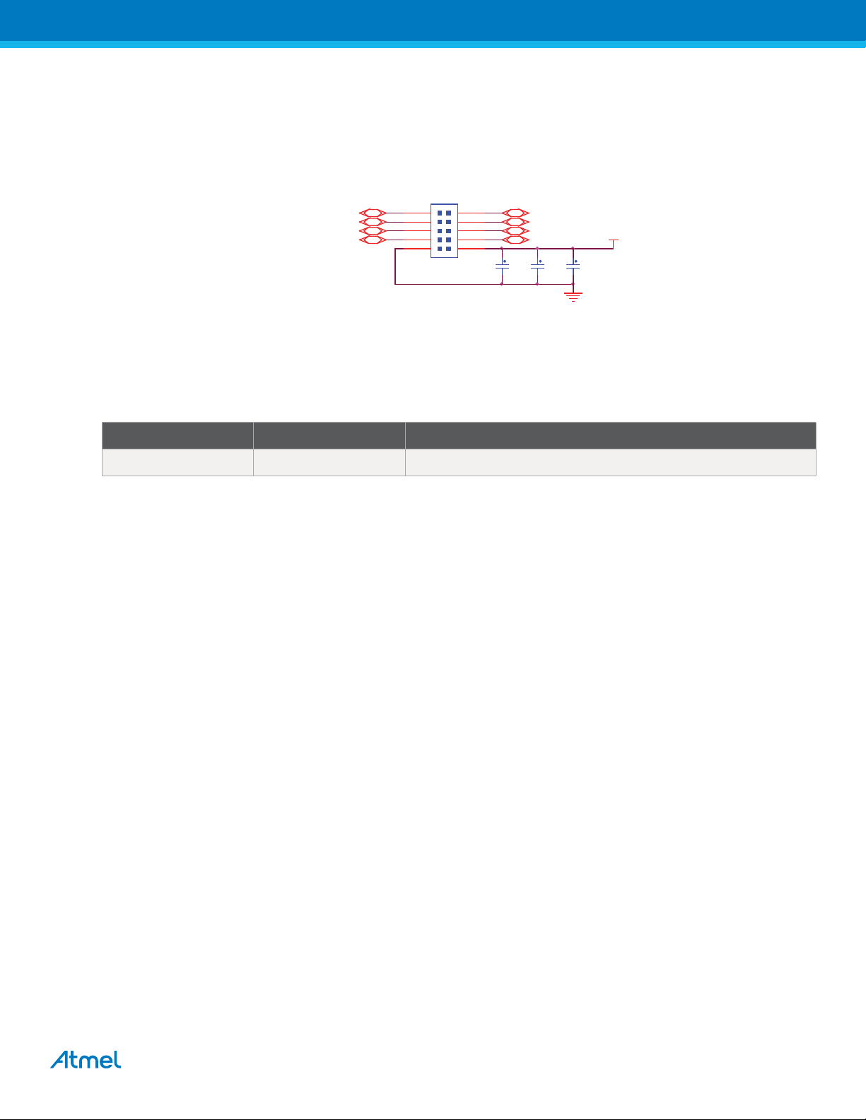
4.2.5 Power Supplies
The Board is driven by 5V input power rail from USB cable or 3 x AAA battery.
The Board embeds all the necessary power rails required for the microcontroller
Table 4-1 summarizes the power specifications.
Table 4-1. Power Rails Associated with the Systems
Nominal Name Powers Component
3.0V VDDIO Partial Peripheral I/O lines on board
3.0V +3V_PERIPH SRAM and image sensor on board
3.0V +3V_LCD LCD and backlight driver on board
1.2V VDDPLL the PLL cell From SAM4S internal LDO
1.2V VDDCORE
3.0V ADVREF analog on board
the core, including the processor, the
embedded memories and the peripherals
From SAM4S internal LDO
SAM4S-WPIR-RD [USER GUIDE]
42060A–ATARM–12/2012
7
Page 10

Figure 4-2. Power Supply
FGND
PC17
R1 47K R3
R2 68K
RV1
V5.5MLA0603
C3
10pF
DGND
C51
100nF
J1
USB Micr o B
5V D- D+ ID G
8
9
123
27R
VBU S
L6 220o hm at 100MHz
C6
33 uF
16V
DGND
PB11
PB10
1 2
475
R4
27R
NSR0320M W2T1G
VBAT
NSR0320M W2T1G
6
RV2
V5.5MLA0603
FGNDDGND
D3
D4
JP8
VIN_SYST EM
VIN_SYST EM
R43 100K
R41 100K
C70
100nF
C58
100nF
DGND
DGND
C59
1uF
C29
1uF
U6
1
IN
2
GND1
EN3GND2
TPS78230DDCR
U5
1
IN
2
GND1
EN3GND2
TPS78230DDCR
OUT
OUT
+3V_LCD
C60
1uF
C57
1uF
JP10
+3VVIN_SYST EM
JP7
JP9
+3V_MCU
+3V_PERIPH
5
4
DGND
5
4
DGND
4.2.6 Memory
The SAM4S features an External Bus Interface (EBI) that permits interfacing to a broad range of external memories and virtually to any parallel peripheral. The SAM4S-WPIR-RD board is equipped with a memory device
connected to the SAM4 EBI:
One SRAM IS62WV10248DBLL
Figure 4-3. Memory
3 cell AAA batter y holder
R46 0R
PC8_WE PC8
C28 33pF
DGND
PC14
NCS0
PC11
NRD
PC8
NWE
U4
JY- 3AA A
+3V_SR AM
R21
470K
R22
47K
PC8
VCC
GND
1
2
DGND
MN3
PC18
PC19
PC20
PC21
PC22
PC23
PC24
PC25
PC26
PC27
PC28
PC29
PC30
PC31
PA18
PA19
PA20
PA0
PA1
PC16
5
A0
4
A1
3
A2
2
A3
1
A4
44
A5
43
A6
42
A7
39
A8
28
A9
27
A10
26
A11
25
A12
24
A13
23
A14
22
A15
21
A16
20
A17
19
A18
18
A19
6
CS1#
40
CS2
41
OE#
17
WE#
NC1
NC2
NC3
NC4
NC5
NC6
NC7
NC8
VDD1
VDD2
GND1
GND2
9
D0
10
D1
13
D2
14
D3
31
D4
32
D5
35
D6
36
D7
7
8
15
16
29
30
37
38
11
33
12
34
DGND
+3V_SR AM
C26
100nF
PC0
PC1
PC2
PC3
PC4
PC5
PC6
PC7
+3V_PER IPH
R25
DNP
3 2
C27
1uF
1
Q2
IRLM L6401
R20
DNP
PC9
IS62WV10248DBLL
DGND
SAM4S-WPIR-RD [USER GUIDE]
42060A–ATARM–12/2012
8
Page 11

4.2.7 JTAG/ICE
Software debug is accessed by a standard 20-pin JTAG connection. This allows connection to a standard USB-toJTAG in-circuit emulator such as SAM-ICE™.
Figure 4-4. JTAG Interface
+3V_MCU
4.2.8 Image Sensor
The CMOS image sensor, OV7740 from OmniVision, used in this reference design is a low-complexity, low-cost,
low-power, yet powerful sensor. It supports VGA (640x480) at up to 60 fps and QVGA (320x240) at up to 120 fps.
The OV7740 has standard interface output pins such as data, horizontal/vertical synchronization signals, pixel
clock output and main clock input. Interfacing between the CMOS image sensor and the SAM4S device is made
easy by means of the sensor interface (parallel capture mode). The SAM4S is able to sample data from the CMOS
image sensor without CPU intervention and transfer image data into internal or external memory.
Figure 4-5. Image Sensor
PB13
PC15
PA4
PA3
PA21
PA23
PA16
PA15
R29
4.7K
+3V_OVT
R30
4.7K
PA21
PA23
PA16
PA15
R63
100K
DGND
PB13
R64 100K
R5 27R
PA24
PA25
PA26
PA27
PA28
PA29
PA30
PA31
14
16
18
20
DGND
PWDN_OVT
MN7
OV7740
D5
XVCLK1
A4
PWDN
B5
RESETB
C4
SIOC
C5
SIOD
C2
FSIN
E6
PCLK
C3
HREF
D1
VSYNC
E5
DATA0
E2
DATA1
D4
DATA2
D3
DATA3
F5
DATA4
F2
DATA5
E4
DATA6
E3
DATA7
D2
DATA8
E1
DATA9
R6
J2
100K
12
34
56
78
910
1112
13
15
17
19
HTST-110-01-SM-DV
DVDD
DGND
DOVDD
DOVDD
DOGND
AVDD
AVDD
AGND
AGND
VREFH
VREFN
IMAGE SENSOR
NC1
NC2
R7
100K
F4
F3
C1
C6
D6
A1
A6
B1
B6
A3
B2
A2
A5
R8
100K
R9
R10
100K
100K
TDI
TMS
TCK
TDO
NRST
+3V_PERIPH
R28
3 2
1
Q3
<REF >
PWDN_OVT
100K
R13 0R
R15 DNP
PC10
0R
R32
+3V_OVT
DNP
0R
C56
C34
DNP
100nF
100nF
DGND
0R
L1
C35
1uF
C41
1uF
C47
1uF
AGND_OVT
C36
100nF
DGND
L2
4.7uH
C42
100nF
C48
1uF
R45 0R
DGND
C37
1uF
C40
1uF
C46
1uF
4.2.9 PIR sensor
The PIR sensor (RE200B from Nicera) chosen for the reference design is a general purpose dual element. This
model satisfies user's cost reduction needs, keeping most dual element type performances at reasonable levels.
SAM4S-WPIR-RD [USER GUIDE]
42060A–ATARM–12/2012
9
Page 12

Figure 4-6. PIR Sensor
U1
1
D
2
S
3
G
RE200B
AGND
R42
47K
ADVREF
R36
10K
AGND
C49
10uF
AGND
ADVREF
R33
1M
R35
1M
AGND
R39 10K
C50
10uF
C45
100nF
R40 10K
R34
10K
R37
1M
C39
10uF
MN8
LT1495CS8
2
3
7
6
5
C33 100nF
R31 1M
IN1-
IN1+
OUT2
IN2-
IN2+
OUT1
VCC
GND
1
AD0, ADC single end input
BN03K314S300R
C44
100nF
B1
R38 0R
8
4
AGND
PA17
ADVREF
DGND
SAM4S-WPIR-RD [USER GUIDE]
42060A–ATARM–12/2012
10
Page 13
4.2.10 ZigBee
The board has a 10-pin male connector for the Atmel RZ600 ZigBee module.
Figure 4-7. ZigBee Interface
4.2.11 LED Indicators
The board has one LED indicator for purposes shown below:
Table 4-2. LED Indicators
Reference Color Function
D1 Blue PIR indicator
4.2.12 LCD
ZB_RSTN
ZB_IRQ
SPIO_NPCS1#
MISO
PB2
PB14
PA12
J5
2X10PTS COU DE
1 2
3 4
5 6
7 8
9 10
C61
18pF
PB3PA5
PA6
PA13
PA14
C62
2.2nF
MISC
SLP_TR
MOSI
SPCK
DGND
C63
2.2uF
+3V_PER IPH
The LCD module gets reset from the NRST signal. As explained, this NRST is shared with the JTAG port. The LCD
chip select signal is connected to NCS2. The SAM4S communicates with the LCD through PIOC where an 8-bit
parallel “8080-like” protocol data bus has to be implemented by software.
SAM4S-WPIR-RD [USER GUIDE]
42060A–ATARM–12/2012
11
Page 14
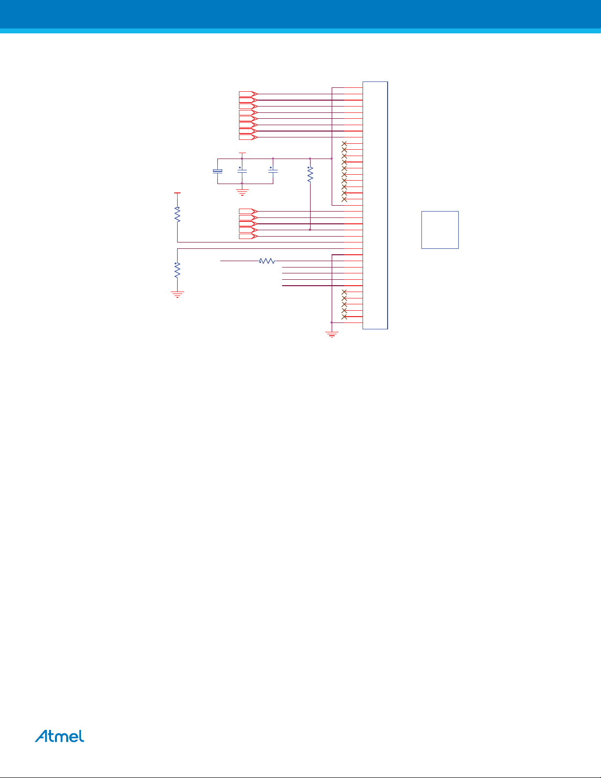
Figure 4-8. LCD Block
A
+3V_LCD
DGND
R54
10K
R57
4.7K
NCS2
+
PC11
PC8
PC19
PA22
NRST
LED_A
PC7
PC6
PC5
PC4
PC3
PC2
PC1
PC0
C52
10uF
+3V_LCD
C53
100nF
DGND
R56 0R
C54
100nF
LED_K1
LED_K2
LED_K3
LED_K4
R44
47K
DGND
J4
FH26- 39S- 0.3SHW
1
VDD
2
DB17
3
DB16
4
DB15
5
DB14
6
DB13
7
DB12
8
DB11
9
DB10
10
DB9
11
DB8
12
DB7
13
DB6
14
DB5
15
DB4
16
DB3
17
DB2
18
DB1
19
DB0
20
VDD
21
RD
22
WR
23
RS
24
CS
25
RESET
26
IM0
27
IM1
28
GND
29
LED- A
30
LEDK1
31
LEDK2
32
LEDK3
33
LEDK4
34
Y+
35
Y-
36
X+
37
X-
38
NC
39
GND
LCD
U7
LCD
YXT28MP002A- 39
4.2.13 Backlight Control
The LCD backlight is made of four integrated white chip-LEDs arranged in parallel. These are driven by an
AAT3155 charge pump, MN10.The AAT3155 is controlled by the SAM4S through a single PIO line PC13 interface;
the 0 Ohm resistor R59 is mounted in series on this line, which permits to use it for other custom purposes. In that
case, the pull-up resistor R58 maintains the charge pump permanently enabled by default.
SAM4S-WPIR-RD [USER GUIDE]
42060A–ATARM–12/2012
12
Page 15

Figure 4-9. Backlight Control
PC13
4.3 Connectors
4.3.1 JTAG/ICE Connector
Figure 4-10. JTAG J2
+3V_LCD
R59
0R
B2
BN03K314S300R
+3V_LC D
R58
47K
DGND
C67
4.7uF
C64
1uF
10
11
9
5
4
MN10
C1+
C1EN/SET
IN
GND
AAT3155IT P
C2+
OUTC P
7
C65
6
C2-
8
3
D1
2
D2
1
D3
12
D4
1uF
LED_A
LED_K1
LED_K2
LED_K3
LED_K4
DGND
C66
1uF
Table 4-3. JTAG/ICE Connector J2 Signal Descriptions
Pin Mnemonic Description
This is the target reference voltage. It is used to check if the target has power,
1 VTref. 3.3V power
2 Vsupply. 3.3V power
nTRST TARGET RESET - Active-low output
3
signal that resets the target
4 GND Common ground
TDI TEST DATA INPUT - Serial data output
line, sampled on the rising edge of the TCK
5
signal.
6 GND Common ground
7 TMS TEST MODE SELECT
8 GND Common ground
to create the logic-level reference for the input comparators, and to control the
output logic levels to the target. It is normally fed from VDD on the target board
and must not have a series resistor.
This pin is not connected in SAM-ICE. It is reserved for compatibility with other
equipment. Connect to VDD or leave open in target system.
JTAG Reset. Output from SAM-ICE to the Reset signal on the target JTAG port.
Typically connected to nTRST on the target CPU. This pin is normally pulled
HIGH on the target to avoid unintentional resets when there is no connection.
JTAG data input of target CPU. It is recommended that this pin is pulled to a
defined state on the target board. Typically connected to TDI on target CPU.
JTAG mode set input of target CPU. This pin should be pulled up on the target.
Typically connected to TMS on target CPU. Output signal that sequences the
target's JTAG state machine, sampled on the rising edge of the TCK signal.
TCK TEST CLOCK - Output timing signal,
for synchronizing test logic and control
9
register access.
JTAG clock signal to target CPU. It is recommended that this pin is pulled to a
defined state on the target board. Typically connected to TCK on target CPU.
SAM4S-WPIR-RD [USER GUIDE]
42060A–ATARM–12/2012
13
Page 16

Pin Mnemonic Description
10 GND Common ground
Some targets must synchronize the JTAG inputs to internal clocks. To assist in
RTCK - Input Return test clock signal from
11
the target.
12 GND Common ground
TDO JTAG TEST DATA OUTPUT - Serial
13
data input from the target.
14 GND Common ground
15 nSRST RESET Active-low reset signal. Target CPU reset signal.
16 GND Common ground
17 RFU This pin is not connected in SAM-ICE.
18 GND Common ground
19 RFU This pin is not connected in SAM-ICE.
20 GND Common ground
meeting this requirement, a returned and retimed TCK can be used to
dynamically control the TCK rate. SAM-ICE supports adaptive clocking which
waits for TCK changes to be echoed correctly before making further changes.
Connect to RTCK if available, otherwise to GND.
JTAG data output from target CPU. Typically connected to TDO on target CPU.
4.3.2 USB Micro AB
Figure 4-11. USB Device Micro-B Connector J1
Table 4-4. USB Device Micro-B Connector J1 Signal Descriptions
Pin Mnemonic Description
1 Vbus 5v power
2 DM Data minus
3 DP Data plus
4 ID Not used
5 GND Common ground
SAM4S-WPIR-RD [USER GUIDE]
42060A–ATARM–12/2012
14
Page 17

4.3.3 ZigBee Socket J5
Figure 4-12. ZigBee Socket J5
Table 4-5. ZigBee Socket J5 Signal Descriptions
Function
Reset /RST 1 2 Misc. Interrupt Request
Interrupt
Request
SPI chip select /SEL 5 6 MOSI SPI MOSI
SPI MISO MISO 7 8 SCLK SPI CLK
Power Supply GND GND 9 10 VCC VCC VCC
Signal
Name
IRQ1 3 4 SLP_TR SLP_TR
Port Pin Pin Port
4.3.4 LCD/TSC Socket J4
Figure 4-13. LCD/TSC Socket J4
Table 4-6. LCD/TSC Socket J4 Signal Descriptions
Signal
Name
Function
Mnemonic Pin Num Pin Num Mnemonic
VDD 3V_INTER 1 2 PC7 LCDDAT17
LCDDAT16 PC6 3 4 PC5 LCDDAT15
LCDDAT14 PC4 5 6 PC3 LCDDAT13
LCDDAT12 PC2 7 8 PC1 LCDDAT11
LCDDAT10 PC0 9 10 NC LCDDAT09
LCDDAT08 NC 11 12 NC LCDDAT07
LCDDAT06 NC 13 14 NC LCDDAT05
LCDDAT04 NC 15 16 NC LCDDAT03
LCDDAT02 NC 17 18 NC LCDDAT01
LCDDAT00 NC 19 20 3V VDD
SAM4S-WPIR-RD [USER GUIDE]
42060A–ATARM–12/2012
15
Page 18

Mnemonic Pin Num Pin Num Mnemonic
RD PC11 21 22 PC8 WR
RS PC19 23 24 PA22 CS
RESET NRST 25 26 PULL UP IM0
IM1 PULL DOWN 27 28 GND GND
LED-A LED-A 29 30 LED-K1 LED-K1
LED-K2 LED-K2 31 32 LED-K3 LED-K3
LED-K4 LED-K4 33 34 NC Y UP
Y DOWN NC 35 36 NC X RIGHT
X LEFT NC 37 38 NC NC
GND GND 39
SAM4S-WPIR-RD [USER GUIDE]
42060A–ATARM–12/2012
16
Page 19

4.4 Schematics
A A
5
PA1
PA2
PA3
PA4
PA5
PA6
PA7
PA8
PA9
PA10
PA11
PA12
PA13
PA14
PA15
EBI_A18
TWI_D0
TWI_CK0
ZB_RST
ZB_SLPTR
XIN32
XOUT32
UART_RXD0
UART_TXD0
Additional CON
SPI_MISO
SPI_MOSI
SPI_SPCK
PIODC_EN1
PA23
PA24
PA25
PA27
PA28
PA29
PA26
PA30
PA31
PIODC_D3
PIODC_D4
PIODC_D5
PIODC_D6
PIODC_D7
4
PB12
PB13
PB14
ERASE
SPI_NPCS1
PIODC_PCK0
PC12
PC13
PC14
PC15
3
PIODC_D2
PB11
PB10
USB_DDP
USB_DDM
PC10
PC11
PIODC_PCLK
PIODC_D0
PIODC_D1
PB7
PB8
PB9
ICE_TCK
XOUT
XIN
PC7
PC8
PC9
PA20
PA21
PA22
EBI_A16
PIODC_FSIN
NCS2_LCD
PB4
PB5
PB6
ICE_TDI
ICE_TDO
ICE_TMS
PC4
PC5
PC6
USER_PB
PA18
PA19
EBI_A14
EBI_A15
PB2
PB3
ZB_IRQ
ZB_MISC
PC2
PC3
PA17
PB1
ACC Low ThresholdPIR_IN_INUT
PC1
B B
I/O MUXING
PA0
PIOA USAGE
EBI_A17
PA16
PIOA USAGE
PIODC_EN2
PB0
PIOB USAGE
ACC High Threshold
PC0
PIOC USAGE
TWI
C C
Image Sensor
PIODC
PIR Sensor
SAM4S (LQFP100)
ADC
D D
5
4
SAM4S-WPIR-RD Block Diagram
ATMEL Cortex M4 Processor
3
2
This agreement is our property. Reproduction and publication without our written authorization shall expose offender to legal proceedings.
This agreement is our property. Reproduction and publication without our written authorization shall expose offender to legal proceedings.
This agreement is our property. Reproduction and publication without our written authorization shall expose offender to legal proceedings.
1
SAM4S-WPIR-RD
SAM4S-WPIR-RD
SAM4S-WPIR-RD
Block Diagram
Block Diagram
Block Diagram
SCALE
SCALE
SCALE
1/1
1/1
1/1
REV. SHEET
REV. SHEET
REV. SHEET
A
A
A
1
1
1
3
3
3
NCS0_SRAM
OVT_RST
PC30
PC31
EBI_A12
EBI_A13
REV
REV
REV
A
A
A
INIT EDIT
INIT EDIT
INIT EDIT
DES.
DES.
DES.
22-FEB-12
22-FEB-12
22-FEB-12
DATE
DATE
DATE
VER.
VER.
VER.
XX-XXX-XXYDL XXX
XX-XXX-XXYDL XXX
XX-XXX-XXYDL XXX
DATEMODIF.
DATEMODIF.
DATEMODIF.
USER_LED
LCD_BL
PC28
PC29
EBI_A10
EBI_A11
SMC_NRD
SW_SRAM
SW_OVT
PC25
PC27
PC26
EBI_A7
EBI_A8
EBI_A9
SMC_NWE
EBI_D6
EBI_D7
PC22
PC23
PC24
EBI_A4
EBI_A5
EBI_A6
EBI_D5
PC21
EBI_A3
EBI_D3
EBI_D4
PC19
PC20
EBI_A1
EBI_A2
EBI_D1
EBI_D2
PC17
PC18
EBI_A0
USB_CNX
EBI_D0
PC16
EBI_A19
PIOC USAGE
SPI
ZigBEE
Battery
USB
8-bit
LCD
SMC
SRAM
2
1
SAM4S-WPIR-RD [USER GUIDE]
42060A–ATARM–12/2012
17
Page 20

A A
B B
C C
D D
5
4
3
2
This agreement is our property. Reproduction and publication without our written authorization shall expose offender to legal proceedings.
This agreement is our property. Reproduction and publication without our written authorization shall expose offender to legal proceedings.
This agreement is our property. Reproduction and publication without our written authorization shall expose offender to legal proceedings.
1
3
3
3
DGND
DGND
SAM4S-WPIR-RD
SAM4S-WPIR-RD
SAM4S-WPIR-RD
Microcontroller
Microcontroller
Microcontroller
REV
REV
REV
SCALE
SCALE
SCALE
A
A
A
INIT EDIT
INIT EDIT
INIT EDIT
1/1
1/1
1/1
DES.
DES.
DES.
22-FEB-12
22-FEB-12
22-FEB-12
DATE
DATE
DATE
VER.
REV. SHEET
VER.
REV. SHEET
VER.
REV. SHEET
A
A
A
XX-XXX-XXYDL XXX
XX-XXX-XXYDL XXX
XX-XXX-XXYDL XXX
DATEMODIF.
DATEMODIF.
DATEMODIF.
2
2
2
DGND
100nF
100nF
DGND
100nF
100nF
C70
C70
TPS78230DDCR
TPS78230DDCR
DGND
R41 100KR41 100K
C58
C58
3
TPS78230DDCR
TPS78230DDCR
GND2
4
R43 100KR43 100K
C59
1uF
C59
1uF
3
GND2
4
C60
1uF
C60
1uF
C28 33pFC28 33pF
C29
1uF
C29
1uF
C57
1uF
C57
1uF
JP9JP9
+3V_PERIPH
VIN_SYSTEM
U6
U6
IN1GND12EN
OUT
5
JP10JP10
+3V_LCD
VIN_SYSTEM +3V +3V_MCU
U5
U5
IN1GND12EN
OUT
5
JP7JP7
R46 0RR46 0R
PC8PC8_WE
PC8 {3}
IS62WV10248DBLL
IS62WV10248DBLL
DGND
NWE
PC8
17
34
100nF
100nF
1uF
1uF
GND112GND2
NRD
PC11
C26
C26
C27
C27
DGND
NCS0
PC14
470K
470K
47K
47K
PA1
PC16
VDD111VDD2
33
DGND
+3V_SRAM
3 2
<REF>Q2<REF>
Q2
DGND
DGND
+3V_MCU +1V2
TEST61PB12_PWML1_ERASE
10
VDDIN
11
VDDOUT
16
VDDCORE
36
VDDCORE
56
VDDCORE
85
VDDCORE
100
VDDPLL
26
GND
45
GND
70
GND
95
GND
2
GND
27
VDDIO
50
VDDIO
69
VDDIO
91
VDDIO
98
VDDIO
PC18
PC20
PC19
MN3
MN3
A05A14A23A32A41A544A643A742A839A928A1027A1126A1225A1324A1423A1522A1621A1720A1819A1918CS1#6CS240OE#41WE#
D09D110D213D314D431D532D635D7
PC1
PC0
PC2
DGND
141618
20
HTST-110-01-SM-DV
HTST-110-01-SM-DV
111213151719
NRST{3}
JP2JP2
+3V_MCU
PB0{3}
PB1{3}
TMS
TCK
JP3JP3
ERASE
87
DGND
TDO
R110R R110R
60
79
76
83
3
5
PB0_PWMH0_AD12B4
NRST
PB6_TMS_SWDIO
PB4_TWD1_PWMH2_TDI
PB5_TWCK1_PWML0_TDO
PB7_TCK_SWCLK
PB1_PWMH1_AD12B5
PB14_NPCS1_PWMH3_DACO1
99
PB14 {3}
PA30_PWML2_NPCS2_MCDA0
PB13_PWML2_PCK0_DACO0
PA31_NPCS1_PCK2_MCDA1
PA29_RI1_TCLK2_MCCK
ADVREF
1
64
81
93
ADVREF
R27 27RR27 27R
PB13 {3}
PA29 {3}
PA30 {3}
PA31 {3}
ADVREF
C8
100nFC8100nF
JP1JP1
3 cell AAA battery holder
JY-3AAAU4JY-3AAA
GND
2
DGND
J2
J2
12345678910
+3V_MCU
100KR6100K
R6
100KR7100K
R7
100KR8100K
R8
100KR9100K
R9
100K
100K
R10
R10
TDI
DGND
PB10
PB11
77
51
PA28_DSR1_TCLK1_MCCDA
63
PA28 {3}
88
89
JTAGSEL
PB10_DDM
PB11_DDP
AT91SAM4S-LQFP100
AT91SAM4S-LQFP100
PA22_TXD1_NPCS3_NCS2_AD12B9
PA19_RK_PWML0_A15_AD12B2
PA20_RF_PWML1_A16_AD12B3
PA26_DCD1_TIOA2_MCDA2
PA21_RXD1_PCK1_AD12B8
PA27_DTR1_TIOB2_MCDA3
PA23_SCK1_PWMH0_A19
PA25_CTS1_PWMH2_A23
PA24_RTS1_PWMH1_A20
59
20
39
24
22
15
57
38
34
PA20
PA21 {3}
PA22 {3}
PA23 {3}
PA24 {3}
PA25 {3}
PA26 {3}
PA27 {3}
+3V_MCU
DGND
U4
VCC
1
DGND
DGND
C5 15pFC5 15pF
PB2{3}
PB3{3}
PB3_UTXD1_PCK2_AD12B7
PA17_TD_PCK1_PWMH3_AD12B0
PA18_RD_PCK2_A14_AD12B1
PA16_TK_TIOB1_PWML2
14
12
18
PA16
PA18
PA19
PA17 {3}
PA16 {3}
VBAT
NSR0320MW2T1G
NSR0320MW2T1G
12MY212M
XOUT
7
9
PB8_XOUT96PB9_XIN
PB2_URXD1_NPCS2_AD12B6
PC13_NWAIT_PWML0_AD12B10
PC15_NCS1PWML1_AD12B11
PC29_A11_TIOA5_AD12B13
PC30_A12_TIOB5_AD12B14
PC31_A13_TCLK5_AD12B15
PA15_TF_TIOA1_PWML3
PA8_CTS0_AD12BTRG
PA11_NPCS0_PWMH0
PA10_UTXD0_NPCS2
PA14_SPCK_PWMH3
PA12_MISO_PWMH1
PA13_MOSI_PWMH2
PA9_URXD0_NPCS1
30
48
44
41
33
46
31
42
28
XOUT32
PA9 {3}
PA10 {3}
PA14
PA15
URXD0
UTXD0
PA11 {3}
PA12 {3}
PA13 {3}
PA14 {3}
PA15 {3}
100nF
100nF
C51
C51
33 uF
33 uF
C6
C6
16V
16V
1 2
NSR0320MW2T1G
NSR0320MW2T1G
D3
D3
D4
D4
JP8JP8
TP4TP4
TP5TP5
TP6TP6
C4 15pFC4 15pF
Y2
XIN
97
PC0_D0_PWML0
PC1_D1_PWML1
PC2_D2_PWML2
PC3_D3_PWML3
PC4_D4_NPCS1
PC5_D5
PC6_D6
PC7_D7
PC8_NWR0_NWE
PC9_NANDOE
PC10_NANDWE
PC11_NRD
PC12_NCS3_AD12B12
PC14_NCS0
PC16_A21_NANDALE
PC17_A22_NANDCLE
PC18_A0_NBS0_PWMH0
PC19_A1_PWMH1
PC20_A2_PWMH2
PC21_A3_PWMH3
PC22_A4_PWML3
PC23_A5_TIOA3
PC24_A6_TIOB3
PC25_A7_TCLK3
PC26_A8_TIOA4
PC27_A9_TIOB4
PC28_A10_TCLK4
PA2_PWMH2_SCK0_DATRG
PA0_PWMH0_TIOA0_A17
PA1_PWMH1_TIOB0_A18
PA4_TWCK0_TCLK0
PA7_RTS0_PWMH3
PA3_TWD0_NPCS3
PA5_RXD0_NPCS3
PA6_TXD0_PCKO
55
49
66
74
72
67
52
53
XIN32
PA0
PA2
PA1
PA3 {3}
PA4 {3}
PA5 {3}
PA6 {3}
DGND
VBUS
L6 220ohm at 100MHzL6 220ohm at 100MHz
PB10
PB11
VIN_SYSTEM
DGND
C2
15pFC215pF
AT91SAM4S-LQFP100
AT91SAM4S-LQFP100
25
47
43
40
37
35
32
29
58
62
65
68
23
21
71
19
73
75
78
80
82
84
86
90
92
94
13
17
54
4
6
8
R2 68KR2 68K
10pFC310pF
DGND FGND
+3V_MCU
TP3TP3
XOUT32
MN1
MN1
C3
27RR327R
27RR427R
+3V
TP2TP2
Y1
32.768 kHzY132.768 kHz
PC0
PC1
PC2
PC3
PC4
PC5
PC6
PC7
PC8_WE
PC9
PC11
PC12
PC14
PC16
PC17
PC18
PC19
PC20
PC21
PC22
PC23
PC24
PC25
PC26
PC27
PC28
PC29
PC30
PC31
PC17
R1 47KR1 47K
V5.5MLA0603
V5.5MLA0603
R3
R4
RV2
V5.5MLA0603
RV2
V5.5MLA0603
TP1TP1
12
XIN32
VIN_SYSTEM
C1
15pFC115pF
PC0 {3}
PC1 {3}
PC2 {3}
PC3 {3}
PC4 {3}
PC5 {3}
PC6 {3}
PC7 {3}
PC10 {3}
PC11 {3}
PC13 {3}
PC15
PC19 {3}
FGND
RV1
RV1
9
1
2
3
4
8
5V D- D+ ID G
5V D- D+ ID G
756
{3}
J1
USB Micro B
J1
USB Micro B
5
4
3
2
1
PA2
PC12
R14
220R
R14
220R
4 2
3
BP1BP1
D1 Blue-ledD1 Blue-led
1
+3V_LCD
+1V2
JP4JP4
VDDCORE
10uF
10uF
C9
C9
+
+
C11 100nFC11 100nF
C12 100nFC12 100nF
C13 2.2uFC13 2.2uF
C14 100nFC14 100nF
C10 100nFC10 100nF
C15 100nFC15 100nF
DGNDDGND
C16 100nFC16 100nF
C17 100nFC17 100nF
C18 100nFC18 100nF
DGND
C19 100nFC19 100nF
C20 100nFC20 100nF
C21 100nFC21 100nF
DGND
C22 100nFC22 100nF
C23 100nFC23 100nF
C24 4.7uFC24 4.7uF
+3V_MCU
C25 4.7uFC25 4.7uF
R21
R21
+3V_SRAM
R22
R22
PC27
PC28
NC17NC28NC315NC416NC529NC630NC737NC8
+3V_PERIPH
PC26
PC25
36
PC7
PC24
PC6
PC23
PC5
PC22
PC4
PC21
PC3
PC31
PA18
PC29
PA19
PC30
PA0
PA20
38
DNP
DNP
0R
R25
R25
1
R20
100K
R20
100K
PC9
SAM4S-WPIR-RD [USER GUIDE]
42060A–ATARM–12/2012
18
Page 21

PA23{2}
PA23
R5 27RR5 27R
DOGND
D6
DGND
R15 DNPR15 DNP
0R
ADVREF
PA3{2}
PA21{2}
PA21
C37
1uF
C37
1uF
C35
1uF
C35
1uF
C36
100nF
C36
100nF
PWDN_OVT
PA4{2}
PC15{2}
SIOCC4SIODC5FSINC2PCLKE6HREFC3VSYNCD1DATA0E5DATA1E2DATA2D4DATA3D3DATA4F5DATA5F2DATA6E4DATA7E3DATA8D2DATA9
DOVDDC1DOVDD
DGND
C6
DGND
L10RL1
0R
3 2
<REF>Q3<REF>
D D
PB13{2}
DGND
R64 100KR64 100K
B5
XVCLK1D5PWDNA4RESETB
DVDD
F3
100nF
100nF
100nF
DNP
DNP
+3V_OVT
Q3
R13 0RR13 0R
PB13
F4
C34
C34
R29
4.7K
R29
4.7K
R30
4.7K
R30
4.7K
R63
100K
R63
100K
PWDN_OVT
MN7
OV7740
MN7
OV7740
C56
C56
R32
DNP
R32
DNP
0R
1
R28
100K
R28
100K
PC10 {2}
+3V_OVT
+3V_PERIPH
5
4
3
AGND
47K
47K
10uF+C52
10uF
100nF
100nF
100nF
100nF
R44
R44
+
C52
C53
C53
C54
C54
RE200BU1RE200B
C C
+3V_LCD
IMAGE SENSOR
AGND_OVT
R45 0RR45 0R
DGND
G
D
S
3
2
R42
47K
R42
47K
XVCLK1
VSYNC
HREF
FSIN
PCLK
PB13
PA15
PA16
PA21
PA23
TP8 SMDTP8 SMD
TP11 SMDTP11 SMD
TP9 SMDTP9 SMD
TP10 SMDTP10 SMD
TP12 SMDTP12 SMD
PA28{2}
PA30{2}
PA29{2}
PA31{2}
E1
NC1A2NC2
A5
C46
1uF
C46
1uF
C47
1uF
C47
1uF
C48
1uF
C48
1uF
U1
1
AGND AGND
PA15{2}
PA16{2}
PA15
PA16
PA26{2}
PA25{2}
PA24{2}
PA27{2}
VREFHA3VREFN
AGNDB1AGND
AVDDA1AVDD
A6
B2
B6
C40
1uF
C40
1uF
C41
1uF
C41
1uF
C42
100nF
C42
100nF
L2
4.7uHL24.7uH
R36
10K
R36
10K
C49
10uF
C49
10uF
A A
DGND
R57
4.7K
R57
4.7K
YXT28MP002A-39A
5
4
YXT28MP002A-39A
ZIGBEE
3
DGND
DGND
LCD
LCD
LCD
18pF
18pF
2.2nF
2.2nF
2.2uF
2.2uF
C61
C61
C62
C62
C63
C63
U7
U7
39
MISO
SPIO_NPCS1# MOSI
PA12{2}
PB14{2}
5 6
7 8
9 10
PA13 {2}
PA14 {2}
SPCK
+3V_PERIPH
ZB_IRQ
ZB_RSTN
PA5{2} PB3 {2}
PB2{2}
1 2
3 4
2X10PTS COUDE
2X10PTS COUDE
PA6 {2}
MISC
SLP_TR
LED_K4
J5
J5
LED_K3
LED_K2
(TWD0)
LED_A
R56 0RR56 0R
LED_K1
(URXD0)
NRST{2}
B B
+3V_LCD
10K
10K
R54
R54
NCS2
PA22{2}
PC19{2}
PC8{2}
PC11{2}
DGND
LCD BACKLIGHT
AAT3155ITP
AAT3155ITP
DGND
4.7uF
4.7uF
4
12
LED_K3
LED_K4
C67
C67
LED_K2
1uF
1uF
PC0{2}
PC1{2}
PC13{2}
+3V_LCD
B2
BN03K314S300R
B2
BN03K314S300R
0R
11
C1-9EN/SET
IN5GND
OUTCP
C2-
D13D22D31D4
8
6
LED_A
LED_K1
C66
C66
PC2{2}
PC3{2}
PC4{2}
PC5{2}
PC6{2}
PC7{2}
DGND
J4
FH26-39S-0.3SHW
J4
FH26-39S-0.3SHW
VDD1DB172DB163DB154DB145DB136DB127DB118DB109DB910DB811DB712DB613DB514DB415DB316DB217DB118DB019VDD20RD21WR22RS23CS24RESET25IM026IM127GND28LED-A29LEDK130LEDK231LEDK332LEDK433Y+34Y-35X+36X-37NC38GND
R590RR59
+3V_LCD
R58
47K
R58
47K
C64
1uF
C64
1uF
10
C1+
MN10
MN10
C2+
7
C65
1uF
C65
1uF
2
This agreement is our property. Reproduction and publication without our written authorization shall expose offender to legal proceedings.
This agreement is our property. Reproduction and publication without our written authorization shall expose offender to legal proceedings.
This agreement is our property. Reproduction and publication without our written authorization shall expose offender to legal proceedings.
1
3
3
3
SAM4S-WPIR-RD
SAM4S-WPIR-RD
SAM4S-WPIR-RD
Peripherals
Peripherals
Peripherals
REV
REV
REV
SCALE
SCALE
SCALE
A
A
A
INIT EDIT
INIT EDIT
INIT EDIT
1/1
1/1
1/1
DES.
DES.
DES.
22-FEB-12
22-FEB-12
22-FEB-12
DATE
DATE
DATE
VER.
REV. SHEET
VER.
REV. SHEET
VER.
REV. SHEET
A
A
A
XX-XXX-XXYDL XXX
XX-XXX-XXYDL XXX
XX-XXX-XXYDL XXX
DATEMODIF.
DATEMODIF.
DATEMODIF.
3
3
3
PA9{2}
PA3{2}
PA11{2}
DGND
2
4
6
8
Additional Connector
8 PIN Connector
8 PIN Connector
8
7
7
4
6
3
5
3
5
PA4 {2}
PB3 {2}
+3V_PERIPH
(TWCK0)
2
1
1
PA10 {2}
(UTXD0)
J6
J6
DGND
R62
649K 1%
R62
649K 1%
AD5, Comparator minus
PB1 {2}
R61
200K 1%
R61
200K 1%
AD4, Comparator plus
PB0 {2}
R60
649K 1%
R60
649K 1%
ADVREF
PIR SENSOR
10uF
10uF
R40 10KR40 10K
5
AGND
DGND
AGND
R39 10KR39 10K
C50
C50
IN2-6IN2+
GND
4
R38 0RR38 0R
1M
100nF
100nF
R371MR37
C45
C45
100nF
100nF
OUT2
C44
C44
1M
C39
10uF
C39
10uF
7
VCC
8
BN03K314S300R
BN03K314S300R
B1
B1
ADVREF
R351MR35
10K
10K
ADVREF
R331MR33
1M
R34
R34
2
3
MN8
LT1495CS8
MN8
LT1495CS8
IN1-
IN1+
OUT1
1
AD0, ADC single end input
TP7 SMDTP7 SMD
PA17 {2}
R31 1MR31 1M
SAM4S-WPIR-RD [USER GUIDE]
42060A–ATARM–12/2012
2
C33 100nFC33 100nF
1
19
Page 22

5.1 Revision History
Document Comments
42060A Initial
Section 5
Revision History
SAM4S-WPIR-RD [USER GUIDE]
42060A–ATARM–12/2012
20
Page 23

Atmel Corporation
1600 Technology Drive
San Jose, CA 95110
USA
Tel: (+1) (408) 441-0311
Fax: (+1) (408) 487-2600
www.atmel.com
Atmel Asia Limited
Unit 01-5 & 16, 19F
BEA Tower, Millennium City 5
418 Kwun Tong Roa
Kwun Tong, Kowloon
HONG KONG
Tel: (+852) 2245-6100
Atmel Munich GmbH
Business Campus
Parkring 4
D-85748 Garching b. Munich
GERMANY
Tel: (+49) 89-31970-0
Fax: (+49) 89-3194621
Atmel Japan G.K.
16F Shin-Osaki Kangyo Bldg
1-6-4 Osaki, Shinagawa-ku
Tokyo 141-0032
JAPAN
Tel: (+81) (3) 6417-0300
Fax: (+81) (3) 6417-0370
Fax: (+852) 2722-1369
© 2012 Atmel Corporation. All rights reserved. / Rev.: 42060A–ATARM–12/2012
Atmel®, Atmel logo and combinations thereof, Enabling Unlimited Possibilities®, and others are registered trademarks or trademarks of Atmel Corporation or its subsidiaries. ARM®, Thumb®, CortexTM are
registered trademarks or trademarks of ARM Ltd. Other terms and product names may be trademarks of others. Other terms and product names may be trademarks of others.
Disclaimer: The information in this document is provided in connection with Atmel products. No license, express or implied, by estoppel or otherwise, to any intellectual property right is granted by this
document or in connection with the sale of Atmel products. EXCEPT AS SET FORTH IN THE ATMEL TERMS AND CONDITIONS OF SALES LOCATED ON THE ATMEL WEBSITE, ATMEL ASSUMES
NO LIABILITY WHATSOEVER AND DISCLAIMS ANY EXPRESS, IMPLIED OR STATUTORY WARRANTY RELATING TO ITS PRODUCTS INCLUDING, BUT NOT LIMITED TO, THE IMPLIED
WARRANTY OF MERCHANTABILITY, FITNESS FOR A PARTICULAR PURPOSE, OR NON-INFRINGEMENT. IN NO EVENT SHALL ATMEL BE LIABLE FOR ANY DIRECT, INDIRECT,
CONSEQUENTIAL, PUNITIVE, SPECIAL OR INCIDENTAL DAMAGES (INCLUDING, WITHOUT LIMITATION, DAMAGES FOR LOSS AND PROFITS, BUSINESS INTERRUPTION, OR LOSS OF
INFORMATION) ARISING OUT OF THE USE OR INABILITY TO USE THIS DOCUMENT, EVEN IF ATMEL HAS BEEN ADVISED OF THE POSSIBILITY OF SUCH DAMAGES. Atmel makes no
representations or warranties with respect to the accuracy or completeness of the contents of this document and reserves the right to make changes to specifications and products descriptions at any time
without notice. Atmel does not make any commitment to update the information contained herein. Unless specifically provided otherwise, Atmel products are not suitable for, and shall not be used in,
automotive applications. Atmel products are not intended, authorized, or warranted for use as components in applications intended to support or sustain life.
 Loading...