

Page 1

SAM4S-EK2
....................................................................................................................
User Guide
11176A–ATARM–24-Sep-12
Page 2

Section 1
Introduction.................................................................................................................1-1
1.1 SAM4S Evaluation Kit........................................................................................................1-1
1.2 User Guide....................................... .......................................................................... ........1-1
1.3 References and Applicable Documents.............................................................................1-1
Section 2
Kit Contents................................................................................................................2-1
2.1 Deliverables ....................................................................................................................... 2-1
2.2 Electrostatic Warning ......................................................................................................... 2-2
Section 3
Power Up....................................................................................................................3-1
3.1 Power up the Board ......... ... ... .... ...................................... .... ... ....................................... ....3-1
3.2 DevStart............................................................................................................................. 3-1
3.3 Recovery Procedure . .... ... ... ... .... ...................................... .... ... ....................................... ... . 3-1
3.4 Sample Code and Technical Support ................................................................................ 3-2
Section 4
Evaluation Kit Hardware.............................................................................................4-1
4.1 Board Overview................... ... ....................................... ... .... ...................................... ........ 4-1
4.2 Features List ...................................................................................................................... 4-2
4.3 Function Blocks.................................................................................................................. 4-2
4.3.1 Processor............................................................................................................. 4-2
4.3.2 Memory................................................................................................................ 4-2
4.3.3 Clock Circuitry. ...................................... .... ... ....................................... ... ... ... ........ 4-3
4.3.4 Reset Circuitry ..................................................................................................... 4-4
4.3.5 Power Supply and Management.......................................................................... 4-4
4.3.6 UART................................................................................................................... 4-5
4.3.7 USART................................................................................................................. 4-5
4.3.8 Display Interface.................................................................................................. 4-6
4.3.9 JTAG/ICE............................................................................................................. 4-8
4.3.10 Audio Interface..................................................................................................... 4-9
4.3.11 USB Device ....................................... ... .... ... ....................................... ... ... ... ...... 4-11
4.3.12 Analog Interface ................................... .... ... ... ....................................... ... ... ...... 4-11
4.3.13 QTouch Elements........... ... ... .... ...................................... .... ... ............................ 4-12
4.3.14 User Buttons................ ... ... ....................................... ... ... ................................... 4-13
4.3.15 LEDs.................................................................................................................. 4-14
4.3.16 SD/MMC Card ................................ ... ... .... ...................................... .... ... ... ......... 4-14
4.3.17 ZigBEE............................................................................................................... 4-14
4.3.18 PIO Expansion................................................................................................... 4-15
SAM4S-EK2 User Guide 1-1
11176A–ATARM–24-Sep-12
Page 3

4.4 Configuration.................................................................................................................... 4-16
4.4.1 PIO Usage ......................................................................................................... 4-16
4.4.2 Jumpers............................................................................................................. 4-19
4.4.3 Test Points......................................................................................................... 4-20
4.4.4 Assigned PIO Lines, Disconnection Possibility.................................................. 4-20
4.5 Connectors....................................................................................................................... 4-22
4.5.1 Power Supply Connector J9 ........ ... ... ... .... ...................................... .... ... ............ 4-22
4.5.2 USART Connector J5 With RTS/CTS Handshake Support............................... 4-22
4.5.3 UART Connector J7 .... ... ....................................... ... ... ...................................... 4-23
4.5.4 USB Device Connector J15...... ... ... ... ... ....................................... ... .... ... ............ 4-23
4.5.5 TFT LCD Connector J8...................................................................................... 4-23
4.5.6 JTAG Debugging Connector J6......................................................................... 4-25
4.5.7 SD/MMC - MCI Connector J3 ............................................................................ 4-26
4.5.8 Analog Connector CN1 & CN2 .......................................................................... 4-27
4.5.9 RS485 Connector J14 ....................................................................................... 4-27
4.5.10 Headphone Connector J11................................................................................ 4-28
4.5.11 ZigBEE Connector J16 ...................................................................................... 4-28
4.5.12 PIO Expansion Port C Connector J12 ............................................................... 4-29
4.5.13 PIO Expansion Port A Connector J13 .............................................................. 4-30
4.5.14 PIO Expansion Port B Connector J14 ............................................................... 4-31
Section 5
Schematics.................................................................................................................5-1
5.1 Schematics......................................................................................................................... 5-1
Section 6
Troubleshooting..........................................................................................................6-1
6.1 Self-Test............................................................................................................................. 6-1
6.2 Board Recovery ........ ....................................... ... .... ... ....................................... ... ... ... ........ 6-1
Section 7
Revision History..........................................................................................................7-1
7.1 Revision History......................................... ... ... ....................................... ... ... .... ................. 7-1
SAM4S-EK2 User Guide 1-2
11176A–ATARM–24-Sep-12
Page 4

1.1 SAM4S Evaluation Kit
The SAM4S Evaluation Kit (SAM4S-EK2) enables evaluation capabilities and code development of
applications running on a SAM4SD32 device.
1.2 User Guide
This guide focuses on the SAM4S-EK2 board as an evaluation platform. It is made up of 6 sections:
Section 1 includes references, applicable documents, acronyms and abbreviations.
Section 2 describes the kit contents, its main features and specif ications.
Section 3 provides instructions to power up the SAM4S-EK2 and describes how to use it.
Section 4 provides board specifications, describes the development environment and presents the
hardware resources, default jumper, switch settings and connectors.
Section 5 provides schematics.
Section 6 provides troubleshooting instructions.
Section 1
Introduction
1.3 References and Applicable Documents
Table 1-1. References and Applicable Documents
Title Comment
SAM4SD32 Datasheet
www.atmel.com
SAM4S-EK2 User Guide 1-1
11176A–ATARM–24-Sep-12
Page 5
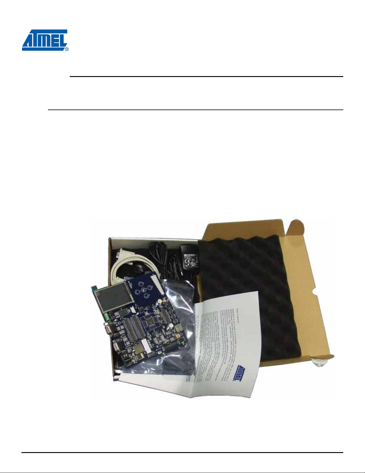
2.1 Deliverables
The Atmel® SAM4S-EK2 toolkit contains the following items:
Board:
– a SAM4S-EK2 board
– a universal input AC/DC power supply with US, Europe and UK plug adapters
Cables:
– one USB cable
– one serial RS232 cable
A Welcome Letter
Figure 2-1. Unpacked SAM4S-EK2
Section 2
Kit Contents
Unpack and inspect the kit carefully. Contact your local Atmel distributor, should you have issues concerning the contents of the kit.
SAM4S-EK2 User Guide 2-1
11176A–ATARM–24-Sep-12
Page 6

2.2 Electrostatic Warning
The SAM4S-EK2 board is shipped in a protective anti-static bag. The board must not be subjected to
high electrostatic potentials. A grounding strap or similar protective device should be worn when handling the board. Avoid touching the components or any other metallic element of the board.
Kit Contents
SAM4S-EK2 User Guide 2-2
11176A–ATARM–24-Sep-12
Page 7

3.1 Power up the Board
Unpack the board taking care to avoid electrostatic discharge. Unpack the power supply, select the right
power plug adapter corresponding to that of your country, and insert it into the power supply.
Connect the power supply DC connector to the board and plug the power supply to an AC power plug.
The board LCD should light up and display a welcome page. Then, click or touch the icons displayed on
the screen and enjoy the demo.
3.2 Sample Code and Technical Support
After boot up, you can run some sample code or your own application on the development kit. You can
download sample code and get technical suppor t from th e Atm el web site : http://www.atmel.com
Section 3
Power Up
SAM4S-EK2 User Guide 3-1
11176A–ATARM–24-Sep-12
Page 8
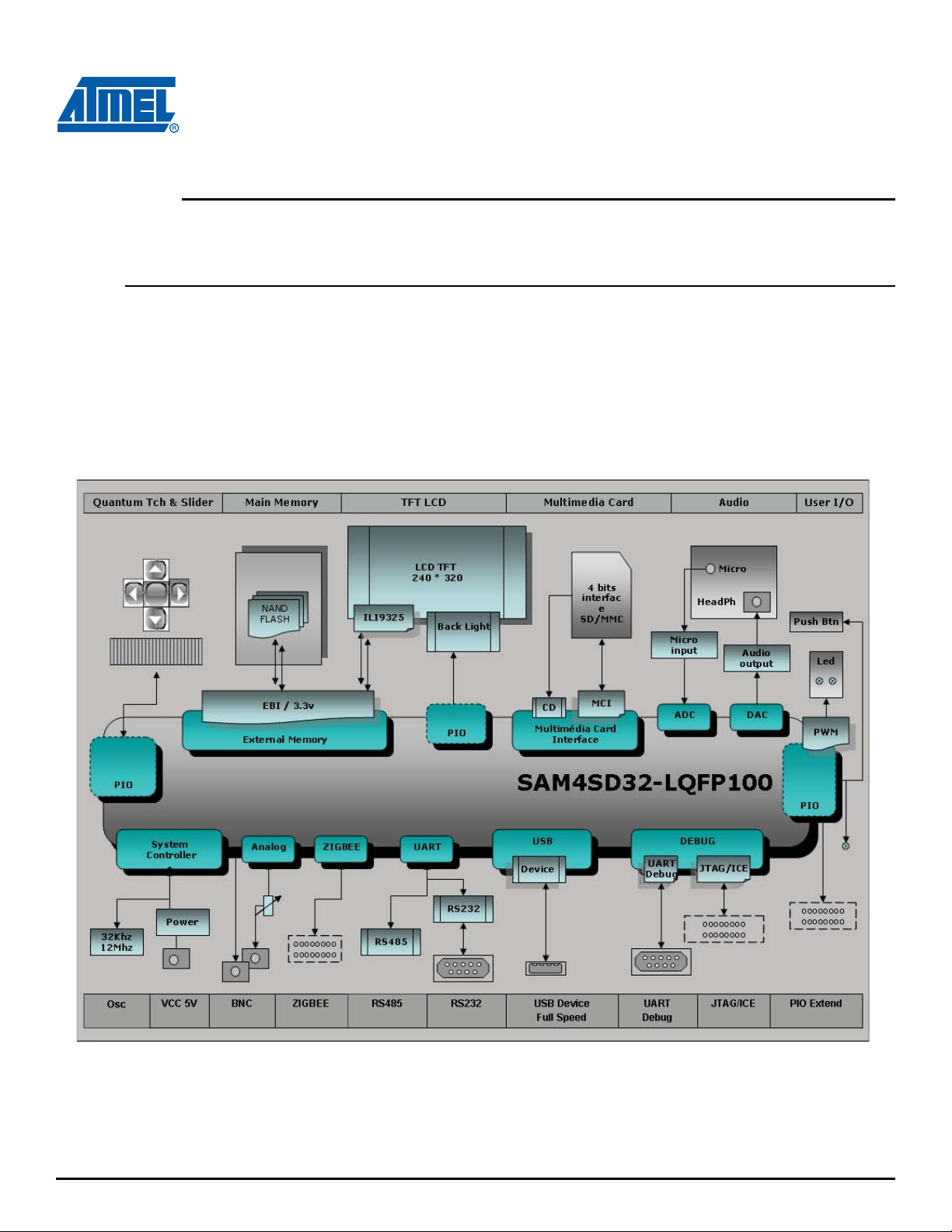
4.1 Board Overview
This section introduces the Atmel SAM4S-EK2 Evaluation Kit design. It introduces system-level concepts, such as power distribution, memory, and interface assignments.
The SAM4S-EK2 board is based on the integration of an ARM
NAND Flash and a set of popular peripherals. It is designed to provide a high performance processor
evaluation solution with high flexibility for various kinds of applications.
Figure 4-1. SAM4S-EK2 Block Diagram
Section 4
Evaluation Kit Hardware
®
Cortex®-M4 processor with on-board
SAM4S-EK2 User Guide 4-1
11176A–ATARM–24-Sep-12
Page 9

4.2 Features List
Here is the list of the main board components and interfaces:
SAM4SD32 chip LQFP100 package with optional socket footprint
12 MHz crystal
32.768 KHz crystal
Optional SMB connector for external system clock input
NAND Flash
2.8 inch TFT color LCD display with touch panel and b acklight
UART port with level shifter circuit
USART port with level shifter circuit multiplexed with RS485 port with level shifter circuit
Microphone input and mono/stereo headphone jack output
SD/MMC interface
Reset button: NRST
User buttons: Left and Right
QTouch
Full Speed USB device port
JTAG/ICE port
On-board power regulation
Two user LEDs
Pow er LED
BNC connector for ADC input
BNC connector for DAC output
User potentiometer connected to the ADC input
ZigBEE connector
2x32 bit PIO connection interfaces (PIOA, PIOC) and 1x16 bit PIO connection interface (PIOB)
®
buttons: Up, Down, Left, Right, Valid and Slider
Evaluation Kit Hardware
4.3 Function Blocks
4.3.1 Processor
The SAM4S-EK2 is equipped with a SAM4SD32 device in LQFP100 package.
4.3.2 Memory
The SAM4SD32 chip embeds:
2048 Kbytes of embedded Flash
160 Kbytes of embedded SRAM
16 Kbytes of ROM with embedded BootLo ader routines (U AR T, USB) and In-Application Programming
functions (IAP) routines
SAM4S-EK2 User Guide 4-2
11176A–ATARM–24-Sep-12
Page 10
Evaluation Kit Hardware
MN3
WE
18
N.C6
6
VCC
37
CE
9
RE
8
N.C11
20
WP
19
N.C5
5
N.C1
1
N.C2
2
N.C3
3
N.C4
4
N.C12
21
N.C13
22
N.C14
23
N.C15
24
R/B
7
N.C17
26
N.C18
27
N.C19
28
I/O0
29
N.C21
34
N.C22
35
VSS
36
PRE
38
N.C23
39
VCC
12
VSS
13
ALE
17
N.C8
11
N.C7
10
N.C9
14
N.C10
15
CLE
16
N.C16
25
N.C20
33
I/O1
30
I/O3
32
I/O2
31
N.C27
47
N.C26
46
N.C25
45
I/O7
44
I/O6
43
I/O5
42
I/O4
41
N.C24
40
N.C28
48
MT29F2G08ABAEA
JP9
Heade r2
C28
100nF
NAND FLASH
PC18
C29
1uF
+3V3
PC14
DGND
R16
47K
R22
0R
DNP
R21 47 K
R19 0R
DGND
+3V3
C27
100nF
PC7
PC6
PC5
PC4
PC0
PC1
PC2
PC3
R15
47K
+3V3
PC10
PC9
PC16
PC17
+3V3
NOT POPULATED
DNP
XOUT32
XIN32
XIN32
XOUT32
PA7
PA8
XIN
XOUT
PB8
PB9
DGND
DGND
DGND
DGND
DGND
R3 DNPR3 DNP
R6 DNPR6 DNP
R9DNPR9DNP
R1 DNPR1 DNP
C3
20pFC320pF
R4 0RR4 0R
C4
20pFC420pF
R2
49.9R 1%R249.9R 1%
Y1Y1
12
3
R8 DNPR8 DNP
R7DNPR7DNP
MN1MN1
PA7_RTS0_PWMH3
49
PA8_CTS0_AD12BTRG
48
PB8_XOUT
96
PB9 _XIN
97
R110RR11
0R
Y212MHzY212MHz
C120pFC120pF
R10 DNPR10 DNP
Y3
32.768KHz
Y3
32.768KHz
12
3
R5 0RR5 0R
R120RR12
0R
J1J1
1
2 3
54
C220pFC220pF
SAM4SD32
The SAM4SD32 features an External Bus Interface (EBI) that permits interfacing to a broad range of
external memories and virtually to any parallel peripheral. The SAM4S-EK2 board is equipped with a
memory device connected to the SAM4 EBI:
One NAND Flash MT29F2G08ABAEA.
Figure 4-2. NAND Flash
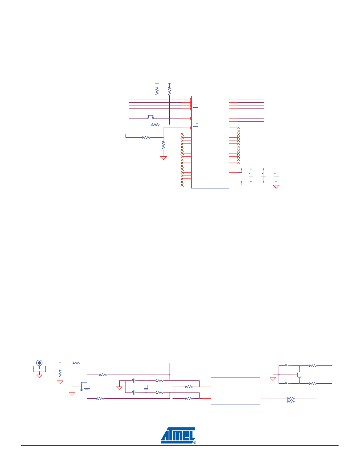
4.3.3 Clock Circuitry
Figure 4-3. External Clock Source
SAM4S-EK2 User Guide 4-3
NCS0 chip select signal is used for NAND Flash chip selection. Furthermore, a dedicated jumper can
disconnect it from the on-board mem ories, thereby letting NCS0 free for other custom purposes.
The clock generator of a SAM4SD32 microcontroller is composed of:
A Low Power 32.768 Hz Slow Clock Oscillator with bypass mode
A 3 to 20 MHz Crystal Oscillator, which can be bypassed (12 MHz needed in case of USB)
A factory programmed fast internal RC Oscillator. 3 output frequencies can be selected: 4 (default
value), 8 or 12 MHz.
A 60 to 130 MHz PLL (PLLB) providing a clock for the USB Full Speed Controller
A 60 to 130 MHz programmable PLL (PLLA), capable to provide the clock MCK to the processor and
to the peripherals. The input frequency of PLLA is from 7.5 to 20 MHz
The SAM4S-EK2 board is equipped with one 12 MHz crystal, optional Piezoelectric Ceramic Resonator
12 MHz (Murata ref. CSTCE12M0G15L99-R0), one 32.768 Hz crystal and an external clock input connector (optional, not populated by default).
11176A–ATARM–24-Sep-12
Page 11
The SAM4SD32 chip internally generates the following clocks:
DGND
+5V
DGND
+5V +3V3
C75
100uF
+
C75
100uF
C65
22uF
+
C65
22uF
C64
100nF
C64
100nF
MN10
BNX002-01
MN10
BNX002-01
SV
1
SG
2
CV
3
CG1
4
CG2
5
CG3
6
C76
100nF
C76
100nF
C66
22uF
+
C66
22uF
MN9
ZEN056V130A24LS
MN9
ZEN056V130A24LS
1
2
3
R92
102K 1%
R92
102K 1%
MN12
MIC29152WU
Micrel's 1.5A LDO, TO263-5
MN12
MIC29152WU
Micrel's 1.5A LDO, TO263-5
VIN
2
VOUT
4
SD
1
GND1
3
ADJ
5
GND2
6
R89
169K 1%
R89
169K 1%
J9
MP179P 2.1mm
J9
MP179P 2.1mm
1
2
3
SLCK, the Slow Clock, which is the only permanent clock of the system
MAINCK, the output of the Main Clock Oscillator selection: either a Crystal Oscillator or a 4/8/12 MHz
Fast RC Oscillator
PLLACK, the output of the Divider and 60 to 130 MHz programmable PLL (PLLA)
PLLBCK, the output of the Divider and 60 to 130 MHz programmable PLL (PLLB)
4.3.4 Reset Circuitry
On-board NRST button BP1 provides an external reset control of th e SAM4SD32.
The NRST pin is bidirectional. It is handled by the on-c hip reset controller. It can be driven low to provide
a reset signal out to the external components. Conversely, it can be asserted low from the outside to
reset the microcontroller Core and the per ipherals. The NRST pin integrates a perma nent pull-up re sistor
of 100 kOhm to VDDIO.
On the SAM4S-EK2 board, the NRST signal is connected to the LCD module and JTAG port.
Note: At power-on, the NRST signal is asserted with a default duration of 2 clock cycles. That duration may not be
Evaluation Kit Hardware
sufficient to correctly reset any other system or board devices connected to that signal. First, in your custom
application, you need to check for these device’s datasheets about reset duration requirements. Then, you
need to set an appropriate configuration in the NRST Manager. This is done through the ERSTL field in the
RSTC_MR register. The NRST duration is thereby configurable between 60 µs and 2 s, whether it is subsequently activated by a software reset or a user reset. Refer to the SAM4SD32 datasheet for in-depth
information.
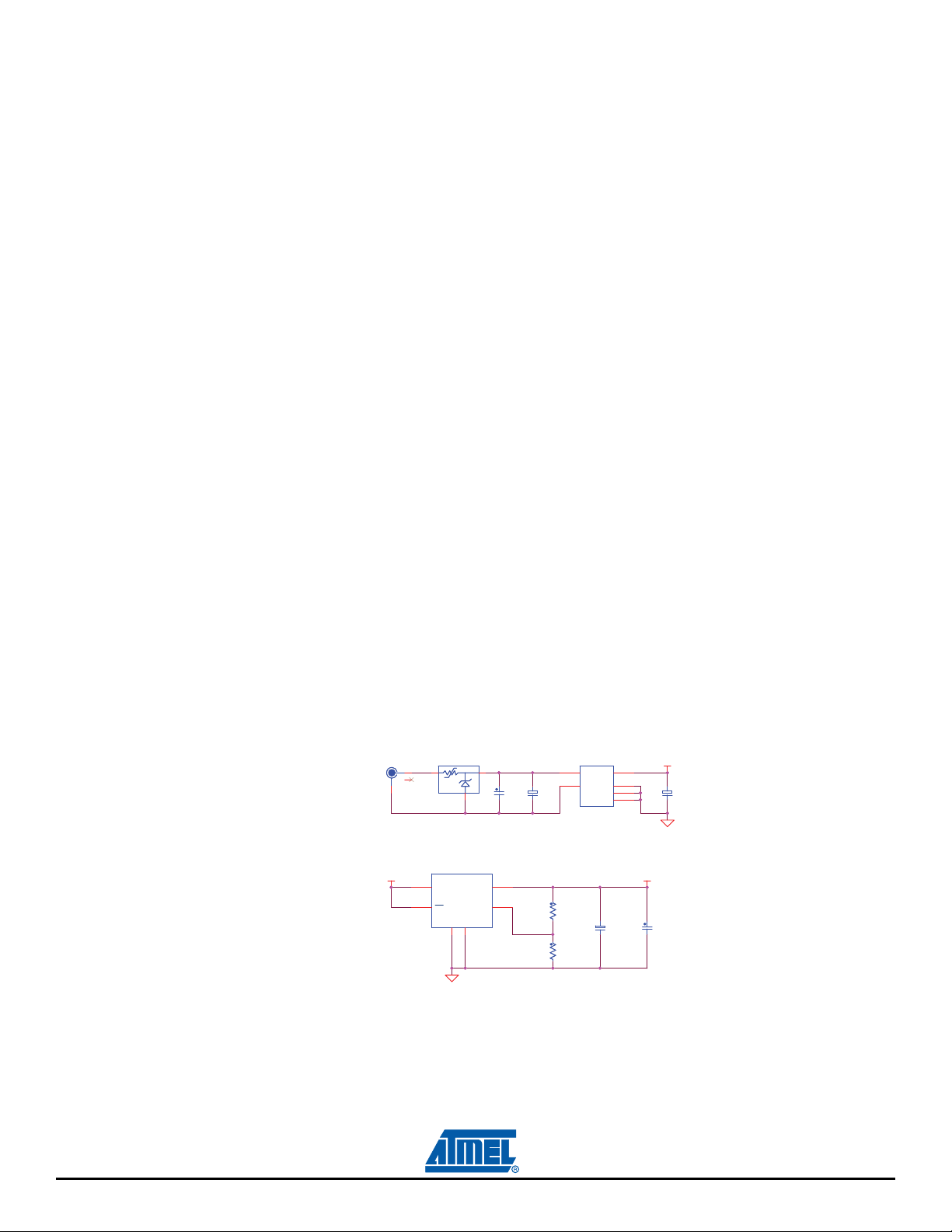
4.3.5 Power Supply and Management
The SAM4S-EK2 board is supplied with an external 5V DC block through input J9. It is protected by a
PolyZen diode (MN9) and an LC combinatory filter (MN10). The PolyZen is used in the event of an incorrect power supply connection.
The adjustable LDO regulator MN12 is used for the 3.3V rail main supply. It powers all the 3.3V components on the board.
Figure 4-4. Power Block
The SAM4SD32 product has different types of power supply pins:
VDDIN pin:
Power for the internal voltage regulator, ADC, DAC, and analog comparator power supplies.
SAM4S-EK2 User Guide 4-4
The voltage ranges from 1.8V to 3.6V.
11176A–ATARM–24-Sep-12
Page 12
4.3.6 UART
Evaluation Kit Hardware
VDDIO pins:
Po wer for the Peripherals I/O lines.
The voltage ranges from 1.62V to 3.6V.
VDDOUT pin:
Output of the internal voltage regulator.
VDDCORE pins:
Power for the core, including the processor, embedded memories and peripherals.
The voltage ranges fr om 1.62V to 1.95V.
VDDPLL pin:
Power for the PLL A, PLL B and 12 MHz oscillator.
The voltage ranges fr om 1.62V to 1.95V.
Note: VDDPLL should be decoupled and filtered from VDDCORE.
The Universal Asynchronous Receiver Transmitter features a two-pin UART that can be used for communication and trace purposes. It offers an ideal channel for in-situ programming solutions. This UART
is associated with two PDC channels to reduce the processor time on packet handling.
This two-pin UART (TXD and RXD only) is buffered through an RS232 Transceiver MN6 and brought to
the DB9 male connector J7.
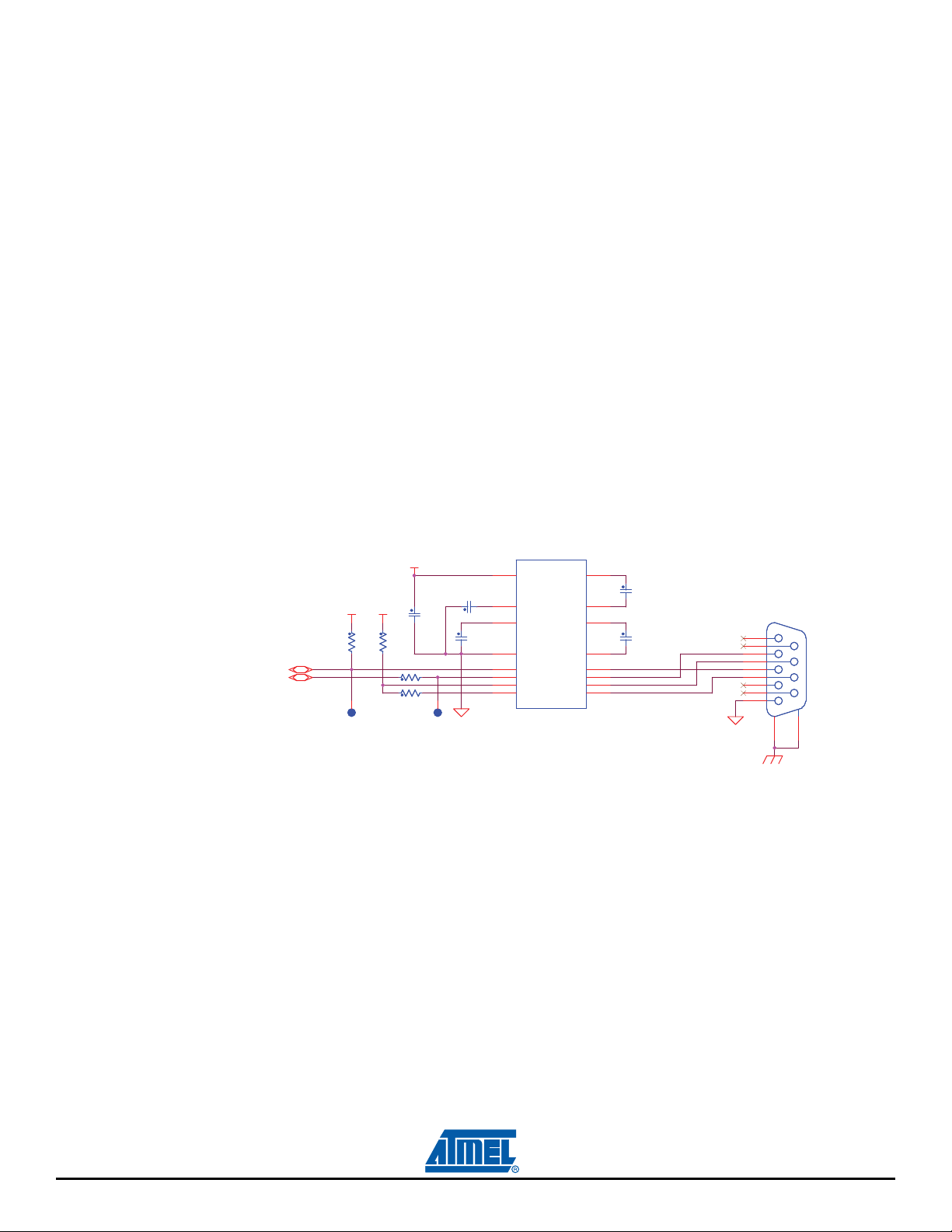
4.3.7 USART
Figure 4-5. UART
MN6
MN6
MAX3232CSE
MAX3232CSE
16
VCC
2
V+
6
V-
15
GND
11
T1IN
12
R1OUT
10
T2IN
9
R2OUT
C1+
C2+
T1OUT
R1IN
T2OUT
R2IN
1
C38
C38
100nF
100nF
3
C1-
4
C42
C42
100nF
100nF
5
C2-
14
13
7
8
DGND
1
6
2
7
3
8
4
9
5
FGND
J7J7
10
11
PA10
PA9
+3V3
TP5
TP5
SMD
SMD
R45
R45
100K
100K
+3V3
R46
R46
100K
100K
R47 0RR47 0R
R48 0RR48 0R
+3V3
C40
C40
100nF
100nF
TP6
TP6
SMD
SMD
DGND
C39
C39
100nF
100nF
C41
C41
100nF
100nF
The Universal Synchronous/Asynchronous Receiver Transmitter (USART) provides one full duplex universal synchronous/asynchronous serial link. The data frame format is extensively configurable (data
length, parity, number of stop bits) to support a broad range of serial communication standards. The
USART is also associated with PDC channels for TX/RX data access.
Note: For design optimization purposes, both tr ansmitters have been implemented on the same
PIO lines, that is PA21, 22, 23, 24, 25.
To avoid any electrical conflict, the RS485 transceiver is isolated from the receiving line PA21.
Should you need to implement an RS485 channel in place of the RS232, follow the procedure below:
1. make sure your software will permanently set PA23 to a high level - this will permanently disable the
RS232 receiver.
2. change JP31 to make sure that 2-3 pins are connected.
SAM4S-EK2 User Guide 4-5
11176A–ATARM–24-Sep-12
Page 13
4.3.7.1 RS232
DGND
DGND
+3V3
J5
5
4
3
2
1
9
8
7
6
10
11
FGND
PA25
DGND
MN5
ADM3312 EARU
C1+
6
C1-
20
C2+
2
C2-
4
C3+
24
C3-
22
VCC
3
V+
1
V-
21
GND
23
SD
19
EN
5
T1IN7T1OUT
18
R1IN
15
R1OUT
10
T2IN8T2OUT
17
R2IN
14
R2OUT
11
T3IN9T3OUT
16
R3IN
13
R3OUT
12
PA24
C34
100nF
PA21_ 232
C31
4.7uF
C35
100nF
R32
47K
PA22
C37
100nF
USART
C33
100nF
R37 47 K
PA23
C36
100nF
C32
100nF
+3V3
R31 0R
R33 0R
R34 0R
R35 0R
R36 0R
R38 0R
+3V3
PA25
PA21_ 485
R23
10K
R25 0R
R30
TBD
DNP
R24
TBD
DNP
+3V3
R26 0R
R27 0R
R28 0R
FGND
R29
120R
MN4
ADM3485 ARZ
RO
1
RE
2
DE
3
DI
4
VCC
8
GND
5
A
6
B
7
JP11
Header2
JP12
Header2
C30
100nF
JP10
Header2
+3V3
DGND
DGND
PA22
RS 485
+3V3
PA24
J4
1
2
3
JP28
Header2 nm
DNP
Evaluation Kit Hardware
SAM4S-EK2 connects the USART1 bus (including TXD, RXD, RTS, CTS handshake signal controls and
EN command) to the DB9 male connector J5 through the RS232 Transceiver MN5.
Figure 4-6. USART Evaluation Kit Hardware
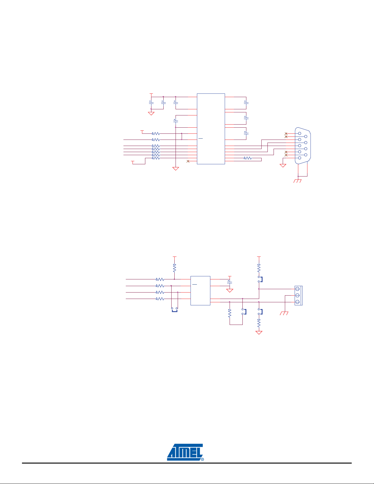
4.3.7.2 RS485
As noticed above, the USART1 is shared with the RS485 port, connected to the transceiver MN4, connected to the 3-point connector J4. The design includes selectable jumpers for RS485 bu s termination
resistors selection (JP10, JP11, JP12).
Figure 4-7. RS485
4.3.8 Display Interface
The SAM4S-EK2 carries a TFT Transmissive LCD module with touch panel, FTM280C34D. Its integrated driver IC is ILI9325. The LCD displa y area is 2.8 inches diagonally me asured, with a native
resolution of 240 x 320 dots.
11176A–ATARM–24-Sep-12
SAM4S-EK2 User Guide 4-6
Page 14
4.3.8.1 LCD Module
LCD_DB3
R59 0R
Six slots on PCB for LCD shield
PC11
R63 4.7 K
DNP
DGND
LED_A
PC26
LCD_DB2
NRST
PC8
LCD_DB0
PC27
LCD
C45
100nF
LCD_DB4
DGND
J8
FH26-39S -0.3SHW
VDD
1
DB1 7
2
DB1 6
3
DB1 5
4
DB1 4
5
DB1 3
6
DB1 2
7
DB1 1
8
DB1 0
9
DB9
10
DB8
11
DB7
12
DB6
13
DB5
14
DB4
15
DB3
16
DB2
17
DB1
18
DB0
19
VDD
20
RD
21
WR
22
RS
23
CS
24
RES ET
25
IM0
26
IM1
27
GND
28
LED-A
29
LEDK1
30
LEDK2
31
LEDK3
32
LEDK4
33
Y+
34
Y-
35
X+
36
X-
37
NC
38
GND
39
PC28
DGND
R49
47K
X_RIGHT
Y_DOWN
Y_UP
X_LEFT
D1
PACDN044Y5 R
TVS, SOT23-5
DNP
1
2
345
NOT POPULAT ED
The part is pl aced as
cl o s e as pos s ibl e t o J8
DGND
PC29
DGND
DGND
DGND
JP13 Header2
LCD_DB9
LCD_DB 13
LCD_DB 12
LCD_DB 11
LCD_DB 10
LCD_DB 16
LCD_DB 15
LCD_DB 14
PC30
LCD_DB 17
R58
4.7K
LCD_DB5
PC2
PC1
PC0
PC3
X_LEFT
LCD_DB9
R56
10K
PC6
PC5
PC4
PC7
PC23
X_RIGHT
+3V3
DGND
DGND
LCD_DB7
Y_DOWN
LCD_DB8
Y_UP
RA2
4.7Kx4
DNP
1
2
3
4 5
6
7
8
PC22
PC31
PC13
LCD_DB6
LCD_DB6
LCD_DB7
DGND
PC15
PC[0 ..31]
LED_K4
LCD_DB8
LCD_DB4
LCD_DB5
LED_K3
LED_K2
PC24
PINs
on
BOT
PIN 39
PIN 1
Z7
FTM28 0C34 D
LCD_DB2
LCD_DB3
LCD_DB1
LED_K1
NRST
RA3
4.7Kx4
DNP
1
2
3
4 5
6
7
8
PC19
LCD_DB0
LCD_DB1
C44
100nF
R61 4.7 K
DNP
DGND
+3V3
+
C43
10uF
PC25
MN8
AAT3155ITP-T1
C1+
10
C1-
9
EN/SET
11
C2+
7
C2-
6
OUTCP
8
IN
5
GND
4
D1
3
D2
2
D3
1
D4
12
C55
1uF
C54
1uF
C57
4.7uF
C56
1uF
R68
0R
R64
47K
LED_A
LED_K1
+3V3
LED_K4
LED_K3
LED_K2
+3V3
PC13
DGND
DGND
TP7
FB1
BN03K314S3 00R
LCD BACKLI GHT
The LCD module gets reset from the NRST sig nal. As expl ained, this NRST is shared with the JTAG port
and the push-button BP1. The LCD chip select signal is connected to NCS1; the jump er JP13 can disconnect it so that this PIO line is available for other custom usage.
The SAM4SD32 communicates with the LCD through PIOC where an 8-bit parallel “8080-like” protocol
data bus has to be implemented in software.
Figure 4-8. LCD Block
Evaluation Kit Hardware
The LCD backlight is made of four integrated white chip-LEDs arranged in parallel. These are driven by
an AAT3155 charge pump, MN8. The AAT3155 is controlled by the SAM4SD32 through a single PIO
line PC13 interface; the 0 Ohm resistor R68 is mounted in series on this line, which permits to use it for
other custom purposes. In that case, the pull-up resistor R64 maintains the charge pump permanently
enabled by default.
On the anode drive line, a 0 Ohm resistor R59 is implemented in series for an optional current limitation.
Figure 4-9. Backlight Control
11176A–ATARM–24-Sep-12
4.3.8.2 Backlight Control
SAM4S-EK2 User Guide 4-7
Page 15
4.3.8.3 Touch Screen Interface
AGND_TP
JP32
Header2
LCD TOUCH SCREEN
R74
0R
C59
100nF
C58
100nF
R71
1R
C60
100nF
TP8
PA14
PA13
PA12
C61
4.7uF
PA11
PA17
TP9
DGND
R65
100K
+3V3
+3V3
AGND_TP
+3V3
R62
100K
R73
100K
R72
100K
L2
10uH-100mA
MN7
ADS7843E
XP
2
YP
3
XM
4
YM
5
DCLK
16
DIN
14
DOUT
12
CS
15
BUSY
13
PE NIRQ
11
VREF
9
VCC1
1
VCC2
10
GND
6
IN3
7
IN4
8
X_RIGHT
Y_DOWN
X_LEFT
Y_UP
R67 0R
R70 0R
R69 0R
PA16
The LCD module integrates a 4-wire touch panel controlled by MN7 (ADS7843) which is a slave device
on the SAM4SD32 SPI bus. The controller sends back the information about the X and Y positions, as
well as a measurement for the pressure applied to the touch panel. The touch panel can be used with
either a stylus or a finger.
The ADS7843 touch panel controller connects to the SPI0 interface via the NPCS0 control signal. Two
interrupt signals are connected and provide events information back to the microcontroller: PenIrq and
Busy.
Note: PenIrq (PA16) is shared with ZigBEE signal IRQ0.
Busy (PA17) is shared with ZigBEE signal IRQ1.
Therefore, if using a ZigBEE interface in concurrence with the TouchScreen controller, take
care not to have both drivers enabled at the same time on either PA16 or PA17.
For that purpose, 0 Ohm resistors have been implemented on these PIO lines in order to disconnect
either end driver from the other:
On the touch panel controller side, R67 and R69.
On ZigBEE side, R117 and R120.
For further information, refer t o the “Schematics” section.
Evaluation Kit Hardware
Touch ADC auxiliary inputs IN3/IN4 of the ADS7843 are connected to test points (TP8, TP9) for optional
function extension.
Figure 4-10. Touch Panel Control
4.3.9 JTAG/ICE
A standard 20-pin JTAG/ICE connector is implemented on the SAM4S-EK2 for the connection of a compatible ARM JTAG emulator interface, such as the SAM-ICE from Segger.
Notes: 1. The NRST signal is connected to BP1 system button and is also used to reset the LCD
module. The 0 ohm resistor R44 may be removed in order to isolate the JTAG port fr om
this system reset signal.
2. The TDO pin is in input mode with the pull-up resistor disabled when the Cortex M4 is
not in debug mode. To avoid current consumption on VDDIO and/or VDDCORE due to
floating input, the internal pull-up resistor corresponding to this PIO line must be
enabled.
11176A–ATARM–24-Sep-12
SAM4S-EK2 User Guide 4-8
Page 16

Figure 4-11. JTAG Interface
+3V3
DGND
NRST
PB5
PB7
PB6
PB4
R43
100K
R43
100K
R41
100K
R41
100K
R39
100K
R39
100K
J6J6
VTref1Vsupply
2
nTRST
3
GND1
4
TDI
5
GND2
6
TMS
7
GND3
8
TCK
9
GND4
10
RTCK
11
GND5
12
TDO
13
GND6
14
nSRST
15
GND7
16
DBGRQ
17
GND8
18
DBGACK
19
GND9
20
R42
100K
R42
100K
R40
100K
R40
100K
R44 0RR44 0R
4.3.10 Audio Interface
The SAM4S-EK2 board supports both audio recording and playback.
The audio volume can be adjusted using the potentiometer RV1, and the microphone amplifier gain can
be adjusted via jumpers (fixed gain of 24 or 26 dB).
4.3.10.1 Microphone Input
The embedded microphone is connected to an audio pr e-ampli fie r using t he TS9 22 ope ratio nal a mplifier
(MN11). The gain is set by using JP14 and JP15 jumpers; both must be set or removed at the same
time.
Evaluation Kit Hardware
By modifying the jumper positions, you can select each of the following gain values:
20 dB (default setting, both JP14 and JP15 are off)
26 dB (both JP14 and JP15 are on).
Notes: 1. R83 is a default 0 Ohm resistor that enables the disconnection of PB0 from the audio
input path for custom usage.
2. The audio pre-amplifier MN11 is powered by a dedicated low dropout regulator
MIC5219-3.3 (MN14).
SAM4S-EK2 User Guide 4-9
11176A–ATARM–24-Sep-12
Page 17

Figure 4-12. Microphone Input
R75 47 K
C74
100nF
C77
4.7uF
R83
0R
R91
0R
AGND
DGND
JP14 and JP15 should be set
or removed tog ether
R90
100K
R76 47 K
AVDD
R93
100K
JP15
Header2
C72
1nF
AGND AG ND
VCC33
C69
1nF
AGND
R77
470R
PB0
R86
47K
AGND
MIC1
SVB6 050
12
MN11
TS922
IN1-
2
IN1+
3
OUT2
7
IN2-
6
IN2+
5
GND
4
VCC
8
OUT1
1
FB2
BN03K314S3 00R
AVDD
R79
1K
JP14 Header2
R87
47K
R81
100R
AVDD
AUDIO IN
C71
22nF
AGND
R82
1K
R78
1K
R80
1K
R84
1K
R85
1K
R88
470R
C62
100pF
C63
22uF
C73
22uF
C67
1uF
C68
1uF
AGND
AGNDAGND
Evaluation Kit Hardware
4.3.10.2 Headphone Output
The SAM4S-EK2 evaluation kit supports mono/stereo audio playback driven by a TPA0223 audio amplifier connected to two DAC channels of the microcontroller.
The TPA0223 is a 2W mono Bridge-Tied-Load (BTL) amplifier desig ned to drive speakers with as low as
4 Ohm impedance. The amplifier can be reconfigured on the fly to drive two stereo Single-Ended (SE)
signals into head phones.
Figure 4-13. Headphone Output
1
AUDIO OUT
+5V
FB3
C79
1uF
DGND
BN03K314S3 00R
JP17 He ader2
C85 0.4 7uF
JP19 He ader2
JP2912
VCC33
PB13
SAM4S-EK2 User Guide 4-10
3
C84 0.4 7uF
TP12
C88 0.4 7uF
AUDIO_OUTL
T est Pad SQ -40T H
VDD_AMP
+
C80
10uF
AGND
R98 33 K
R99 47 K
R100 33K
R104 47K
R105 33K
C82
100nF
MN13
TPA0223DGQ
3
VDD
5
RIN
1
MONO-IN
9
LIN
11
AGND
RO/MO+
LO/MO-
ST/MN
SHUTD0WN
BYPA SS
GND
PAD
6
10
7
2
4
8
+
C81 220uF-TAN-6.3V
R95 1K
R97 1K
AGND
+
C83 220uF-TAN-6.3V
R101 100K R102 100K
R103 100K
C86 0.4 7uF
AGND
AGND
2
5
4
3
2
1
AGND
JP20
Header2
11176A–ATARM–24-Sep-12
J10
J11
Phone jack Stereo 3.5
VDD_AMP
C87
1uF
AGND
Page 18

Using a readily available 1/8-in. (3,5 mm) stereo headphone jack, the control switch is closed when no
C94
10pF
R116 27R
DGND
RV2
V5.5MLA0 603
PC21
PB11
FGND
RV1
V5.5MLA0 603
USB
5V D- D+ ID G
J15
TBD USB Micro B
1
23475
6
8
9
10 11
R112 68K
DGND
R110 47K
FGND
R114 27R
PB10
ADVREF
DGND
DGND
VCC33
+5V
JP2JP2
1
2
3
C5
100nFC5100nF
ADVREF
1
R13
2.2K
R13
2.2K
MN2
LM4040-2.5
MN2
LM4040-2.5
SAM4SD32
plug is inserted. When closed, a 100-kOhm/1-kOhm divi der pulls the ST/MN input low. When a jack plug
is inserted, the 1-kOhm resistor is disconnected and the ST/MN input is pulled high. The mono speaker
(J10 connector) is also physically disc on ne cted from the RO/MO+ output so that no so un d is h ea r d fr om
the speaker while the headphones are inserted.
4.3.11 USB Device
The SAM4SD32 UDP port is compliant with the Universal Serial Bus (USB) rev 2.0 Full Speed device
specification. J15 is a micro B-type receptacle for USB device.
Both 27-Ohm resistors R114 and R116 build up a 90-Ohm differential impedance together with the
(embedded) 6-Ohm output impedance of the SAM4SD32 full speed channel drivers.
R110 and R112 build up a divider bridge from VBUS +5V to implement plug-in detection (5V level gets
lowered to a PIO compatible 3.3V level) through PC21.
Figure 4-14. USB
Evaluation Kit Hardware
4.3.12 Analog Interface
4.3.12.1 Analog Reference
SAM4S-EK2 User Guide 4-11
The 2.5V voltage reference is based on a LM40 40 (Precision Micropower Shunt Voltage Reference).
This ADVREF level can be set as 2.5V or 3.3V via the jumper JP2.
Figure 4-15. Analog Vref
11176A–ATARM–24-Sep-12
Page 19

4.3.12.2 Analog Input
The BNC connector CN1 is connected to the ADC port PB1 as an exte rnal analog input. An on-board 50Ohm resistor termination can be applied by closing jumper JP16. A low pass filter can be implemented
for the BNC connector CN1 by replacing R94 and C78 with custom resisto r and capacitor values,
depending on your application requirements.
A 10-KOhm potentiometer (VR1) is also connected to this channel to implemen t an easy access to ADC
programming and debugging (or implement an analog user control like display br ightness, volume, etc.) .
Either of these two functions can be selected by jumper JP18.
Figure 4-16. ADC Input
CN1
BNC
JP16
Header2
R96
49.9R
R94
0R
C78
10nF
Evaluation Kit Hardware
4.3.12.3 Analog Output
The BNC connector CN2 is connected to the DAC port PB13 and provides an extern al analog output . An
on-board 50-Ohm resistor termination can be enabled by closing jumper JP21. A filter can be implemented on this output channel by replacing R106 and C90 with appropriate resistor and capacitor
values, depending on the application requirements.
Figure 4-17. DAC Output
CN2
BNC
VR1
10K V R
DGND
VCC33
1 3
DGND
JP21
Header2
R109
49.9R
Potentiometer
Clockwise 2-->3
2
C89
10nF
C90 2.2uF
R106
0R
AUDIO_OUTL
JP18
JP30
ADC
3
1
3
1
AD5
2
2
PB1
DAC1
PB13
DGND
DAC
4.3.13 QTouch Elements
QTouch keys consist in a series of sensors formed by the association of a copper area and the capacitive effect of human fingers approaching it.
4.3.13.1 Keys
The SAM4S-EK2 implements five individual capacitive touch keys (UP, DOWN, RIGHT, LEFT and
VALID) using five pairs of PIO.
SAM4S-EK2 User Guide 4-12
11176A–ATARM–24-Sep-12
Page 20
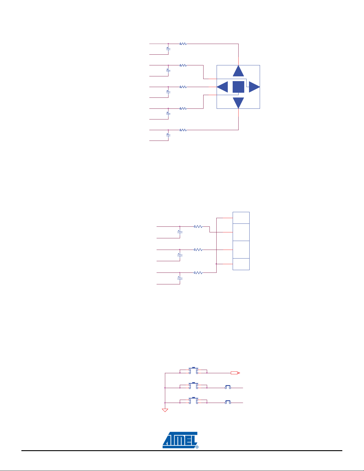
4.3.13.2 Slider
PC25
PC24
PC31
PC30
PC29
PC28
PC23
PC22
PC27
PC26
R53 1KR53 1K
C49
22nF
C49
22nF
R60 1KR60 1K
R51 1KR51 1K
R57 1KR57 1K
C51
22nF
C51
22nF
R55 1KR55 1K
C47
22nF
C47
22nF
K1
DNPK1DNP
C53
22nF
C53
22nF
C52
22nF
C52
22nF
PB3
PC12
DGND
NRST
JP26JP26
BP1BP1
1
4
2
3
BP3BP3
1
4
2
3
JP25JP25
BP2BP2
1
4
2
3
Evaluation Kit Hardware
Figure 4-18. QST Keys
A group of channels forms a Slider. A Slider is composed of three channels for a QTouch acquisition
method using three pairs of PIOs. Such a sensor is used t o det ect a line ar finger displa ceme nt on a sensitive area. A typical implementation is volume control.
Figure 4-19. QT_Slider
4.3.14 User Buttons
There are two mechanical user buttons on the SAM4S-EK2, which are connected to PIO lines and
defined to be "left" and "right" buttons by default.
In addition, a mechanical button controls the system reset, signal NRST.
Figure 4-20. System Buttons
PA1
PA0
PA3
PA2
PA5
PA4
22nF use X7R
R50 1K
C46
22nF
R52 1K
C48
22nF
R54 1K
C50
22nF
S1
QT ouch Slider
SR
SL
SM
SR
SAM4S-EK2 User Guide 4-13
11176A–ATARM–24-Sep-12
Page 21
4.3.15 LEDs
PA19
PA20
PC20
+3V3
DGND
D4Red-ledD4Red-led
R113
220R
R113
220R
Q1
IRLML2502
Q1
IRLML2502
1
3
2
R115 100KR115 100K
D3 Green-ledD3 Green-led
R117
220R
R117
220R
R111
220R
R111
220R
D2Blue-ledD2Blue-led
There are three LEDs on the SAM4S-EK2 board:
A blue LED (D2) and a green LED (D3), which are user def ined and controlled by the GPIO.
A red LED (D4), which is a power LED indicating that the 3. 3V power rail is active . It is also controlled
by the GPIO and can be treated as a user LED as well. The only difference with the two others is that
it is controlled through a MOS transistor . By default, the PIO line is disabled; a pull-up resistor controls
the MOS to light the LED when the power is ON.
Figure 4-21. LEDs
4.3.16 SD/MMC Card
Evaluation Kit Hardware
4.3.17 ZigBEE
The SAM4S-EK2 has a high-speed 4-bit multimedia MMC interface, which is connected to a 4-bit
SD/MMC micro card slot featuring a card detection switch.
Figure 4-22. SD Card
+3V3
123
PA26
PA27
PA28
PA29
PA30
PA31
PA6
R126 0R
R127 0R
R20 0R
R124 0R
R125 0R
R17
10K
R18
10K
45
678
RA1
68Kx4
+
C26
C25
100nF
10uF
DGND
SD CARD
J3
TF01A
1
DAT2
2
DAT3
3
CMD
4
VCC
5
CLK
6
VSS
7
DAT0
8
DAT1
10
GND
9
CD
Sh1
Sh2
Sh3
11
12
13
DGND
SAM4S-EK2 has a 10-pin male connector for the RZ600 ZigBEE module.
Note: 0 Ohm resistors have been implemented in series with the PIO lines that are used else-
where in the design, thereby enabling their individual disconnection, should a conflict occur
in your application.
SAM4S-EK2 User Guide 4-14
11176A–ATARM–24-Sep-12
Page 22

Figure 4-23. ZigBEE Interface
+5V
PA18
+3V3
JP23
1
2
3
JP24
1
2
3
PA19
+5V +5V
+3V3
+3V3
+3V3
PIO A
+3V3
PA20
DGND
JP22
1
2
3
+3V3 +3V3 +3V3 +3V3
PC0
PC1
PC2
PC4
PC3
PC5
PC6
J13
1 2
3 4
5 6
7 8
9 10
11 12
13 14
15 16
17 18
19 20
21 22
23 24
25 26
27 28
29 30
31 32
33 34
35 36
37 38
39 40
PC8
PC7
PC9
PC12
PC11
PC10
PC15
PC14
PC13
PC17
PC19
PC20
PC16
PC21
PB6
PC18
PB7
PB3
PB1
PB0
PB4
PB2
PB5
PB11
PB9
PB14
PB13
PB8
PB12
PB10
PA13
PA14
PA11
PA9
PA6
PA7
PA15
PA10
PA12
PA8
PA23
PA27
PA22
PA25
PA30
PA29
PA24
PA28
PA21
PA31
PA26
J12
1 2
3 4
5 6
7 8
9 10
11 12
13 14
15 16
17 18
19 20
21 22
23 24
25 26
27 28
29 30
31 32
33 34
35 36
37 38
39 40
PC[0..31]
PA[0..31]
PB[0..14]
DGNDDGND
DGND
DGND
DGND
PIO C
PA16
PIO B
J14
1 2
3 4
5 6
7 8
9 10
11 12
13 14
15 16
17 18
19 20
21 22
23 24
PA17
ZB_RST N
IRQ1_Z BEE
SPIO_N PCS2 #
MISO
PA18
PA17
PB2
R118 0R
R119 0R
J16
HE 1 0 5 x2
1 2
3 4
5 6
7 8
9 10
R120 0R
R121 0R
C95
18pF
C96
2.2nF
PA16
PA15
PA13
PA14PA12
C97
2.2uF
Evaluation Kit Hardware
IRQ0_Z BEE
SLP_TR
MOSI
SPCK
JP27
Header2
+3V3
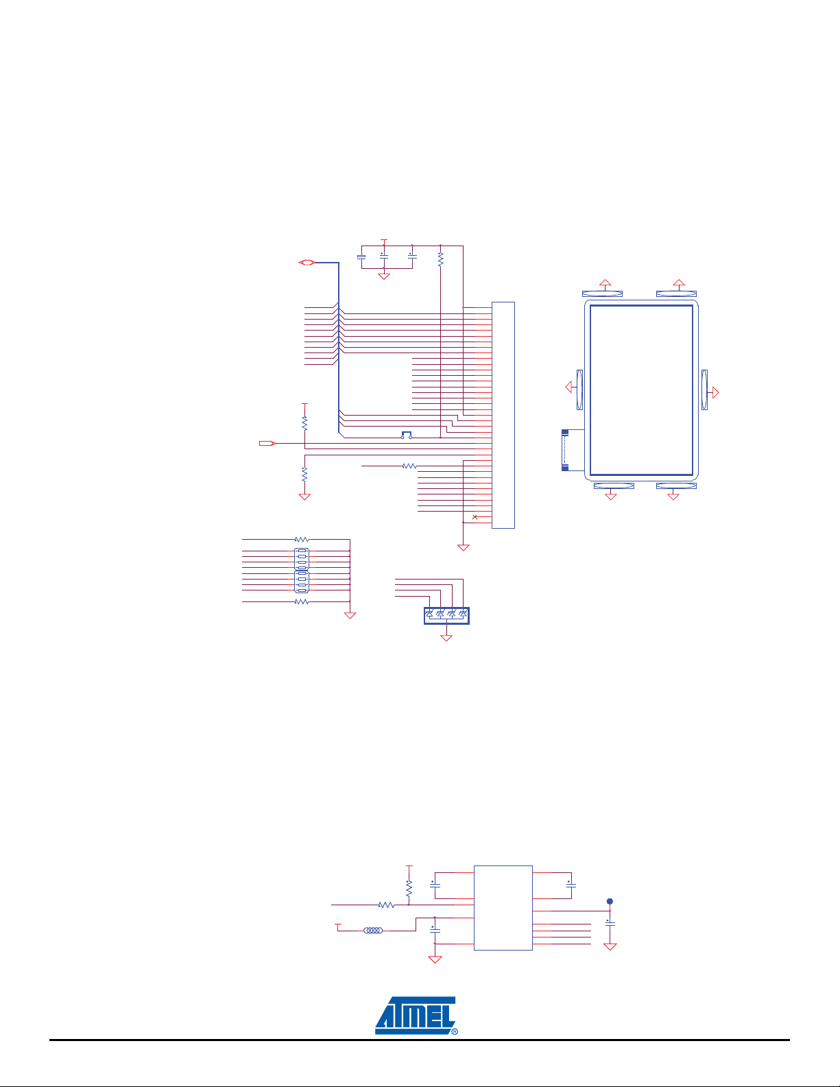
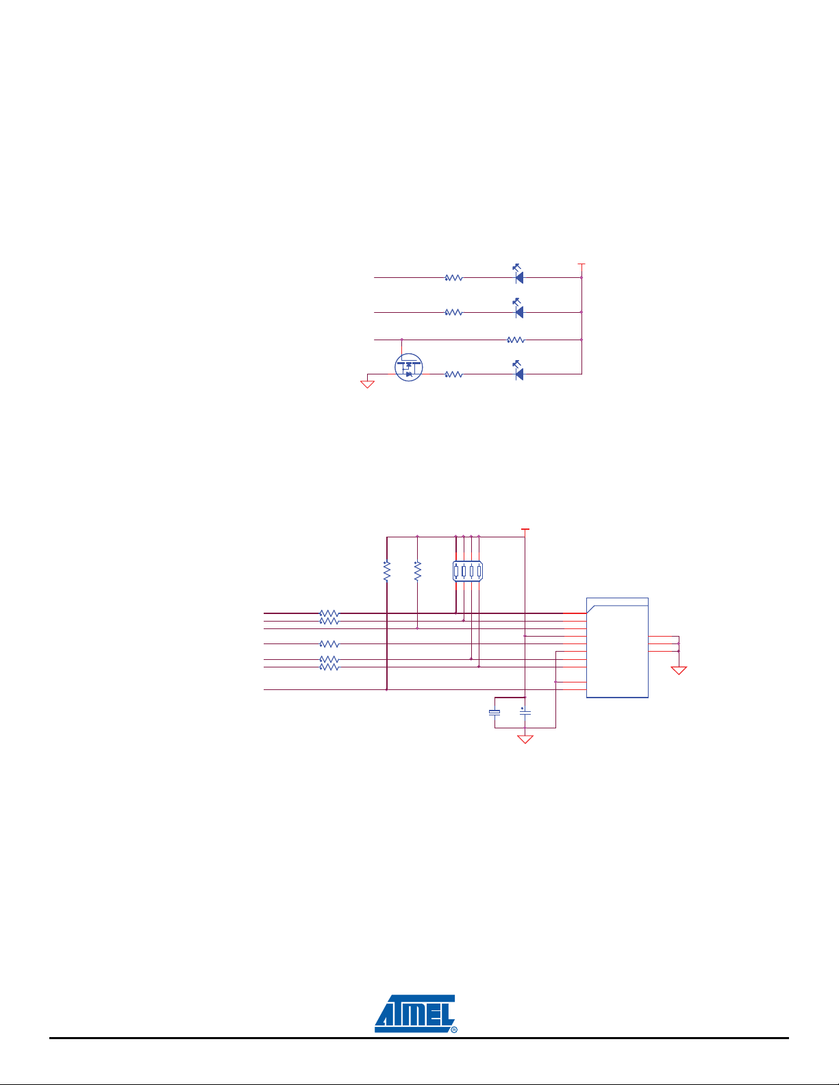
4.3.18 PIO Expansion
The SAM4S-EK2 product features three PIO controllers, PIOA, PIOB and PIOC, which are multiplexed
with the I/O lines of the embedded periphera ls. Each PIO Co ntroller cont rols up to 32 lines (16 f or PIOB).
Expansion ports J12, J13 and J14 provide PIO lines access for customer defined usage.
Figure 4-24. PIO Expansion
ZI GBEE
DGND
Note: All PIO lines are available on these expansion con nec t or s, exc ep t th ose tha t ar e use d for
the QTouch elements.
SAM4S-EK2 User Guide 4-15
11176A–ATARM–24-Sep-12
Page 23

4.4 Configuration
This section describes the PIO usage, the jumpers, the test p oints and the solder d rops of a SAM4S-EK2
board.
4.4.1 PIO Usage
Table 4-1. PIO Port A Pin Assignments and Signal Descriptions
Evaluation Kit Hardware
I/O
No
Line
1 PA0 PWMH0 TIOA0 A17 WKUP0 QTouch slider (left) SNS
2 PA1 PWMH1 TIOB0 A18 WKUP1 QTouch slider (left) SNSK
3 PA2 PWMH2 SCK0 DATRG WKUP2 QTouch slider (middle) SNS
4 PA3 TWD0 NPCS3 QTouch slider (middle) SNSK
5 PA4 TWCK0 TCLK0 WKUP3 QTouch slider (right) SNS
6 PA5 RXD0 NPCS3 WKUP4 QTouch slider (right) SNSK
7 PA6 TXD0 PCK0 MCI card detection
8 PA7 RTS0 PWMH3 XIN32 CLK32KHz
9 PA8 CTS0
10 PA9 URXD0 NPCS1 PWMFI0 WKUP6 UART receive data
11 PA10 UTXD0 NPCS2 UART transmit data
12 PA 11 NPCS0 PWMH0 WKUP7 NPCS0# (TSC)
13 PA12 MISO PWMH1 MISO_TSC ZigBEE MISO
14 PA13 MOSI PWMH2 MOSI_TSC ZigBEE MOSI
15 PA14 SPCK PWMH3 WKUP8 SPCK_TSC ZigBEE CLK
16 PA15 TF TIOA1 PWML3 WKUP14 / PIO_DCEN1 ZigBEE SLPTR
17 PA16 TK TIOB1 PWML2 WKUP15 / PIO_DCEN2 IRQ_TSC ZigBEE IRQ0
Peripheral APeripheral BPeripheral
C Extra Function
AD12BTR
G
System
Function Comment
WKUP5 XOUT32 CLK32KHz
18 PA17 TD PCK1 PWMH3 AD0 BUSY_TSC ZigBEE IRQ1
19 PA18 RD PCK2 A14 AD1 ZigBEE RSTN
20 PA19 RK PWML0 A15 AD2/ WKUP9 Blue LED (UserLED1)
21 PA20 RF PWML1 A16 AD3/ WKUP10 Green LED (UserLED2)
22 PA21 RXD1 PCK1 AD8 USART RXD
23 PA22 TXD1 NPCS3 NCS2 AD9 USART TXD
24 PA23 SCK1 PWMH0 A19 POI_DCCLK USART transceiver enable
25 PA24 RTS1 PWMH1 A20 POI_DC0 USART RTS
26 PA25 CTS1 PWMH2 A23 POI_DC1 USART CTS
27 PA26 DCD1 TIOA2 MCDA2 POI_DC2 MCI data bit 2
28 PA27 DTR1 TIOB2 MCDA3 POI_DC3 MCI data bit 3
29 PA28 DSR1 TCLK1 MCCDA POI_DC4 MCI command
SAM4S-EK2 User Guide 4-16
11176A–ATARM–24-Sep-12
Page 24
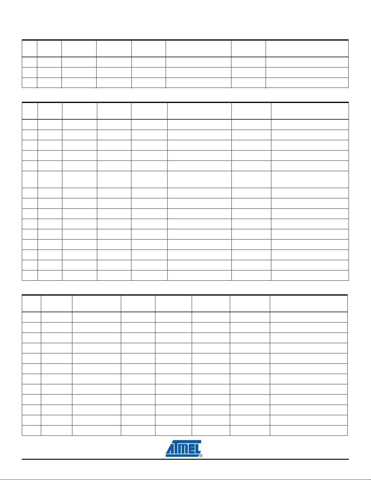
Table 4-1. PIO Port A Pin Assignments and Signal Descriptions (Continued)
Evaluation Kit Hardware
I/O
No
Line
30 PA29 RI1 TCLK2 MCCK POI_DC5 MCI clock
31 PA30 PWML2 NPCS2 MCDA0 WKUP11 / POI_DC6 MCI data bit 0
32 PA31 NPCS1 PCK2 MCDA1 POI_DC7 MCI data bit 1
Peripheral APeripheral BPeripheral
C Extra Function
System
Function Comment
Table 4-2. PIO Port B Pin Assignments and Signal Descriptions
I/O
No
Line
1 PB0 PWMH0 AD4 Microphone input
2 PB1 PWMH1 AD5 Analog input
3 PB2 URXD1 NPC S2 AD6 / WKUP12 ZigBee chip select
4 PB3 UTXD1 PCK2 AD7 User push-button 1
5 PB4 TWD1 PWMH2 TDI JTAG data in
6 PB5 TWCK1 PWML0 WKUP13
7PB6 TMS/SWDIO JTAG test mode select
8PB7 TCK/SWCLK JTAG clock
9PB8 XOUT CLK12MHz
Peripheral APeripheral BPeripheral
C Extra Function
System
Function Comment
TDO/
TRACESWO
JTAG data out
10 PB9 XIN CLK12MHz
11 PB10 DDM USB DM
12 PB11 DDP USB DP
13 PB12 PWML1 ERASE Flash erase selector
14 PB13 PWML2 PCK0 DAC0 Audio Output R
15 PB14 NPCS1 PWMH3 DAC1 Audio Output L
Table 4-3. PIO Port C Pin Assignments and Signal Descriptions
Peripheral BPeripheral
No I/O Line Peripheral A
1 PC0 D0 PWML0 EBI D0
2 PC1 D1 PWML1 EBI D1
3 PC2 D2 PWML2 EBI D2
4 PC3 D3 PWML3 EBI D3
5 PC4 D4 NPCS1 EBI D4
6 PC5 D5 EBI D5
7 PC6 D6 EBI D6
8 PC7 D7 EBI D7
9 PC8 NWR0/NWE TFT LCD write enable
C
Extra
Function
System
Function Comments
10 PC9 NANDOE NAND Flash output enable
11 PC10 NANDWE NAND Flash write enable
12 PC11 NRD TFT LCD read enable
SAM4S-EK2 User Guide 4-17
11176A–ATARM–24-Sep-12
Page 25

Table 4-3. PIO Port C Pin Assignments and Signal Descriptions (Continued)
Evaluation Kit Hardware
No I/O Line Peripheral A
Peripheral BPeripheral
C
Extra
Function
System
Function Comments
13 PC12 NCS3 AD12 User push-button 2
14 PC13 NWAIT PWML0 AD10 LCD backlight control
15 PC14 NCS0 NAND Flash chip select
16 PC15 NCS1 PWML1 AD11 TFT LCD chip select
17 PC16 A21/NANDALE NAND Flash ALE
18 PC17 A22/NANDCLE NAND Flash CLE
19 PC18 A0/NBS0 PWMH0 RDYBSY NAND Flash RDY/BSY
20 PC19 A1 PWMH1 TFT LCD RegSel
21 PC20 A2 PWMH2 Red LED (Power)
22 PC21 A3 PWMH3 USB Vbus detection
23 PC22 A4 PWML3 QTouch valid button SNS
24 PC23 A5 TIOA3 QTouch valid button SNSK
25 PC24 A6 TIOB3 QTouch up button SNS
26 PC25 A7 TCLK3 QTouch up button SNSK
27 PC26 A8 TIOA4 QTouch down button SNS
28 PC27 A9 TIOB4 QTouch down button SNSK
29 PC28 A10 TCLK4 AD13 QTouch left button SNS
30 PC29 A11 TIOA5 AD14 QTouch left button SNSK
31 PC30 A12 TIOB5 QTouch right button SNS
32 PC31 A13 TCLK5 QTouch right button SNSK
SAM4S-EK2 User Guide 4-18
11176A–ATARM–24-Sep-12
Page 26

Evaluation Kit Hardware
4.4.2 Jumpers
The SAM4S-EK2 board jumpers are essentially used for two main purposes: functional selection or current measurement. Details are given below.
Table 4-4. Jumpers Setting
Designation Label Default Setting Feature
JP1 JTAG OPEN Close to select the JTAG boundary scan of the SAM4SD32
JP2 ADVREF 1-2
JP3 ERASE OPEN Close to reinitialize the Flash contents and some of its NVM bits.
JP4 TEST
JP5 VDDPLL CLOSE Access for current measurement on VDDPLL
JP6 VDDIO CLOSE Access for current measurement on VDDIO
JP7 VDDIN CLOSE Access for current measurement on VDDIN
JP8 VDDCORE CLOSE Access for current measurement on VDDCORE
JP9 CE FLASH CLOSE NCS0 enable NAND Flash chip select
JP10 RS485 OPEN Maintain differential impedance for RS485 interface
JP11 RS485 CLOSE Maintain impedance matching for RS485 interface
JP12 RS485 OPEN Maintain differential impedance for RS485 interface
JP13 CS CLOSE NCS1 chip select LCD
JP14 - JP15 MIC GAIN0
JP16 ADC input OPEN Close for impedance matching on ADC BNC port
JP17 – JP19 MIC Gain stage Close to mux RIN/LIN into MONO-IN path within audio PA
JP18 SELECT ADC INP
JP20 MONO/STEREO CLOSE Close to fix in mono speaker, no matter the stereo plug state
JP21 DAC output OPEN Close for impedance matching on DAC BNC port
Not populated
(OPEN)
CLOSE (both) 20db
OPEN (both) 26db
1-2
2-3
Analog reference voltage selection between 3.3V (close 1-2) and
2.5V (close 2-3)
Close for manufacturing test or fast programming mode
Close both to lower gain stage on microphone input.
ADC input potentiometer
ADC input BNC
JP22
JP23
JP24
JP25 BP2 CLOSE Open to disconnect and free PB3 for custom usage
JP26 BP3 CLOSE Open to disconnect and free PC12 for custom usage
JP27 ZIGBEE CLOSE
SAM4S-EK2 User Guide 4-19
PIO expansion J12
voltage supply
PIO expansion J13
voltage supply
PIO expansion J14
voltage supply
2-3 Set to 3.3V (position 1-2 sets to 5V)
2-3 Set to 3.3V (position 1-2 sets to 5V)
2-3 Set to 3.3V (position 1-2 sets to 5V)
Power supply connection/disconnection for the ZigBEE module
May also be used as a current measurement point
11176A–ATARM–24-Sep-12
Page 27

Table 4-5. Audio Input Configuration
4.4.3 Test Points
Some test points have been placed on the SAM4S-EK2 board for the verif ication of important signals.
Table 4-6. Test Points
Reference Function
TP1, TP2, TP3, TP4 GND
Evaluation Kit Hardware
JP17 JP19 MONO-STEREO INPUT
OFF OFF PIN test point (TP12)
OFF ON Left-in only
ON OFF R i g ht -i n on l y
ON ON Sum of Left-in and Right-in
TP5
TP6
TP7
TP8, TP9
TP12 Optional Audio PA input
UART TXD
UART RXD
LCD Backlight driver anode
Aux ADC input for TSC
4.4.4 Assigned PIO Lines, Disconnection Possibility
As pointed out in some previous interface description, 0 Ohm resistors ha ve been inser ted on the pat h of
the receiver PIO lines of the SAM4S-EK2. These are the PIO lines connected to an external driver on the
board. The 0 Ohm resistors allow disconnecting each of these fo r custom usage (throug h PIO expansion
connectors for example). This feature gives the user an added level of versatility for prototyping a system
of his own. See the table below.
Table 4-7. Disconnecting Possibility
Designation Default Assignment PIO
R19 0R PC18, RDY/BSY on NAND Flash
R20 0R PA29
R22 DNP Optional write protection on NAND Flash
R25 0R PA21_485
R26 0R PA25
R27 0R PA24
R28 0R PA22
R31 0R PA23
R33 0R PA22
R34 0R PA21_232
R35 0R PA24
R36 0R PA25
R44 0R NRST
SAM4S-EK2 User Guide 4-20
11176A–ATARM–24-Sep-12
Page 28
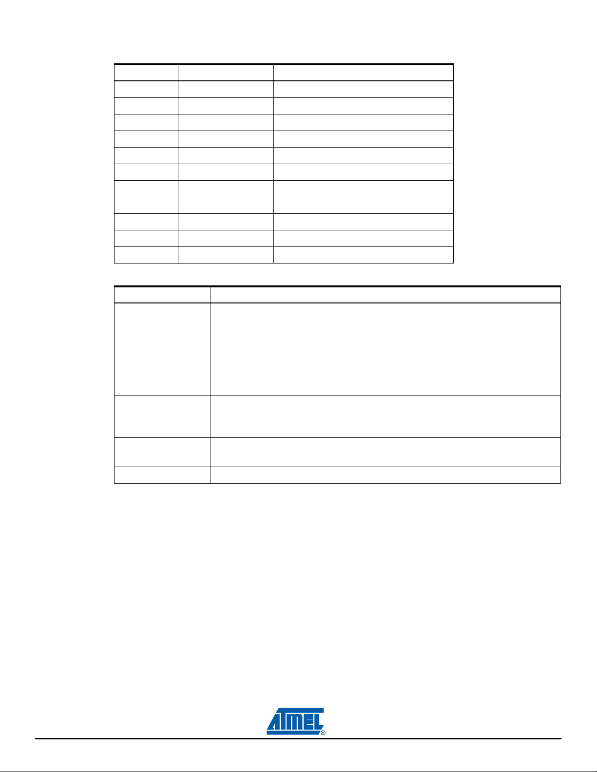
Table 4-7. Disconnecting Possibility
Designation Default Assignment PIO
R47 0R PA9
R48 0R R2OUT/MN5
R59 0R LCD backlight LED anode
R67 0R PA17
R68 0R PC13
R69 0R PA16
R70 0R Vref TSC
R118 0R PA18 ZB_RSTN
R119 0R PA17 IRQ1_ZBEE
R120 0R PA16 IRQ0_ZBEE
R121 0R PA15 SLP_TR
Table 4-8. Default Not Populated Parts
Reference Function
J1, R1
Y1, R3, R7
R6, R8
R9, R10
JP1, JP4
C13
J2
External clock resource input
Backup 12 MHz crystal
Isolation between 12 MHZ clock source and GPIO line
Isolation between 32 kHz clock source and GPIO line
JTAGSEL and TEST selector
Coupling capacitor
LQFP100 Socket
Evaluation Kit Hardware
R22
R24, R30
JP28
D1
R61, R63, RA2, RA3
R122, R123 Optional TWI
Optional write protection on NAND Flash
Differential impedance matching for RS485 cable
Option for software test
Optional ESD protection for LCD touch panel
Optional databus termination for LCD controller
SAM4S-EK2 User Guide 4-21
11176A–ATARM–24-Sep-12
Page 29

4.5 Connectors
4.5.1 Power Supply Connector J9
The SAM4S-EK2 evaluation board can be powered from a 5V DC power supply connected to the external power supply jack J9. The positive pole is the center pin.
Figure 4-25. Power Supply Connector J9
Evaluation Kit Hardware
Table 4-9. Power Supply Connector J9 Signal Descriptions
Pin Mnemonic Signal Description
1 Center +5 VCC
2 Gnd Ground reference
4.5.2 USART Connector J5 With RTS/CTS Hands hak e Su pp or t
Figure 4-26. Male RS232/USART Connector J5
Table 4-10. Serial COM1 Connector J5 Signal Descriptions
Pin Mnemonic Signal Description
1, 4, 6, 9 NC NO CONNECTION
2 TXD TRANSMITTED DATA RS232 serial data output signal
3 RXD RECEIVED DATA RS232 serial data input signal
5GND GROUND
7 RTS READY TO SEND Active-positive RS232 input signal
8 CTS CLEAR TO SEND Active-positive RS232 output signal
SAM4S-EK2 User Guide 4-22
11176A–ATARM–24-Sep-12
Page 30

4.5.3 UART Connector J7
Figure 4-27. Male RS232/UART connector J7
Table 4-11. Male RS232/UART Connector J7 Signal Descriptions
Pin Mnemonic Signal Description
1, 4, 6, 7, 8, 9 NC NO CONNECTION
2 TXD TRANSMITTED DATA RS232 serial data output signal
3 RXD RECEIVED DATA RS232 serial data input signal
5 GND GROUND
4.5.4 USB Device Connector J15
Evaluation Kit Hardware
Figure 4-28. Micro-B USB Connector J15
Table 4-12. Micro-B USB Connector J15 Signal Descriptions
Pin Mnemonic Signal Description
1Vbus5V power
2 DM Data 3 DP Data +
4 Gnd Ground
5 Shield Shield
4.5.5 TFT LCD Connector J8
One 39-pin connector is available on the board to connect the LCD module, backlight and touch screen.
Figure 4-29. LCD Connector J8
SAM4S-EK2 User Guide 4-23
11176A–ATARM–24-Sep-12
Page 31

Table 4-13. LCD Connector J8 Signal Descriptions
Pin Mnemonic Pin Mnemonic
1 3.3V 2 LCD_DB17 (PC7)
3 LCD_DB16 (PC6) 4 LCD_DB15 (PC5)
5 LCD_DB14 (PC4) 6 LCD_DB13 (PC3)
7 LCD_DB12 (PC2) 8 LCD_DB11 (PC1)
9 LCD_DB10 (PC0) 10 LCD_DB09 (NC)
11 LCD_DB08 (NC) 12 LCD_DB07
13 LCD_DB06 (NC) 14 LCD_DB05 (NC)
15 LCD_DB04 (NC) 16 LCD_DB03 (NC)
17 LCD_DB02 (NC) 18 LCD_DB01 (NC)
19 LCD_DB00 (NC) 20 3.3V
21 RD (PC11) 22 WR (PC8)
23 RS (PC19) 24 CS (PC15)
25 RESET 26 IM0
27 IM1 28 GND
Evaluation Kit Hardware
29 LED-A 30 LED-K1
31 LED-K2 32 LED-K3
33 LED-K4 34 Y UP
35 Y DOWN 36 X RIGHT
37 X LEFT 38 NC
39 GND
SAM4S-EK2 User Guide 4-24
11176A–ATARM–24-Sep-12
Page 32

4.5.6 JTAG Debugging Connector J6
This JTAG connector is a 20-way Insulation Displacement Connector (IDC) keyed box header (2.54 mm
male) that mates with IDC sockets mounted on a ribbon cable. Its signal assignment is compatible with
the SAM-ICE or any similar third-party interface.
Figure 4-30. JTAG/ICE Connector J6
Table 4-14. JTAG/ICE Connector J6 Signal Descriptions
Pin Mnemonic Description
This is the target reference voltage. It is used to check if the target has power, to
1 VTref. 3.3V power
create the logic-level ref erence for the input comparators and to control the output
logic lev els t o the target . It is normally fed from Vdd on the target board and must
not have a series resistor.
Evaluation Kit Hardware
2 Vsupply. 3.3V power
nTRST TARGET RESET — Active-low
3
4 GND Common ground.
5
6 GND Common ground.
7 TMS TEST MODE SELECT
8 GND Common ground.
9
10 GND Common ground.
11
12 GND Common ground.
output signal that resets the target
TDI TEST DATA INPUT — Serial data
output line, sampled on the rising edge
of the TCK signal
TCK TEST CLOCK — Output timing
signal, for synchronizing test logic and
control register access
RTCK
Input Return test clock signal from the
target
This pin is not connected in SAM-ICE. It is reserved for compatibility with other
equipment. Connect to Vdd or leave open in target system.
JTAG Reset. Output from SAM-ICE to the Reset signal on the target JTAG port.
Typically connected to nTRST on the target CPU. This pin is normally pulled
HIGH on the target to avoid unintentional resets when there is no connection.
JTAG data input of target CPU. It is recommended that this pin is pulled to a
defined state on the target board. Typically connected to TDI on target CPU.
JTAG mode set input of target CPU. This pin should be pulled up on the target.
Typically connected to TMS on target CPU. Output signal that sequences the
target’s JTAG state machine, sampled on the rising edge of the TCK signal.
JTAG clock signal to target CPU. It is recommended that this pin is pulled to a
defined state on the target board. Typically connected to TCK on target CPU.
Some targets must synchronize the JTAG inputs to internal clocks. To assist in
meeting this requirement, a returned and retimed TCK can be used to
dynamically control the TCK rate. SAM-ICE supports ada ptive clocking which
waits for TCK changes to be echoed correctly before making further changes.
Connect to RTCK if available, otherwise to GND.
13
14 GND Common ground.
SAM4S-EK2 User Guide 4-25
TDO JTAG TEST DATA OUTPUT —
Serial data output from the target
JTAG data output from target CPU. Typically connected to TDO on target CPU.
11176A–ATARM–24-Sep-12
Page 33
Table 4-14. JTAG/ICE Connector J6 Signal Descriptions (Continued)
Pin Mnemonic Description
15 nSRST RESET — Active-low reset signal. Target CPU reset signal.
16 GND Common ground.
17 RFU This pin is not connected in SAM-ICE.
18 GND Common ground.
19 RFU This pin is not connected in SAM-ICE.
20 GND Common ground.
4.5.7 SD/MMC - MCI Connector J3
Figure 4-31. SD/MMC Connector J3
Evaluation Kit Hardware
Table 4-15. SD/MMC Connector J3 Signal Descriptions
Pin Mnemonic Pin Mnemonic
1 RSV/DAT3 2 CDA
3GND4VCC
5CLK6GND
7 DAT0 8 DAT1
9 DAT2 10 Card Detect
11 GND 12
SAM4S-EK2 User Guide 4-26
11176A–ATARM–24-Sep-12
Page 34
4.5.8 Analog Connector CN1 & CN2
Figure 4-32. Analog Input Connector CN1 and Analog Out put CN2, Bottom View
Table 4-16. Analog Input, Output Connector CN1, CN2 Signal Descriptions
Pin Mnemonic
1, 2, 3, 4 GND
5 Analog input PB1 for CN1 and analog output PB13 for CN2 respectively
4.5.9 RS485 Connector J14
Evaluation Kit Hardware
Figure 4-33. RS485 Connector J14
Table 4-17. RS485 J14 Signal Descriptions
Pin Mnemonic
1 A - non-inverted RS485 signal A
2 Frame ground
3 B - non-inverted RS485 signal B
SAM4S-EK2 User Guide 4-27
11176A–ATARM–24-Sep-12
Page 35
4.5.10 Headphone Connector J11
Figure 4-34. Headphone J11
Table 4-18. Headphone J11 Signal Descriptions
Pin Mnemonic
1AGND
2 Out left
3
4
5 Out Right
Evaluation Kit Hardware
4.5.11 ZigBEE Connector J16
Figure 4-35. ZigBee Connector J16
Table 4-19. Connector J16 Signal Descriptions
Signal
Function
Reset /RST 1 2 Misc.
Interrupt
Request
Name Port Pin Pin Port
IRQ 3 4 SLP_TR SLP_TR
Signal
Name Function
Option on Misc. Port Set by
Zero Ohm Resistor or Sold er Shun ts
EEPROM for MA C addr ess, CAP arr a y
settings and serial number
TST: test mode activation
CLKM: RF chip clock output
SPI chip
select
SPI MISO MISO 7 8 SCLK SPI CLK
Power
Supply
SAM4S-EK2 User Guide 4-28
/SEL 5 6 MOSI SPI MOSI
GND GND 9 10 VCC VCC VCC
Voltage range: 1.8V to 5.5V, typically
regulated to 3.3V
11176A–ATARM–24-Sep-12
Page 36

4.5.12 PIO Expansion Port C Connector J12
Figure 4-36. PIO Expansion Connector J12
Table 4-20. Connector J12 Signal Descriptions
Pin Mnemonic Pin Mnemonic
1 +5V or +3.3V 2 +5V or +3.3V
3 GND 4 GND
5 PC0 6 PC16
7 PC1 8 PC17
9PC210PC18
11 PC3 12 PC19
13 PC4 14 PC20
Evaluation Kit Hardware
15 PC5 16 PC21
17 PC6 18 NC
19 PC7 20 NC
21 PC8 22 NC
23 PC9 24 NC
25 PC10 26 NC
27 PC11 28 NC
29 PC12 30 NC
31 PC13 32 NC
33 PC14 34 NC
35 PC15 36 NC
37 GND 38 GND
39 3.3V 40 3.3V
SAM4S-EK2 User Guide 4-29
11176A–ATARM–24-Sep-12
Page 37
4.5.13 PIO Expansion Port A Connector J13
Figure 4-37. PIO Expansion Connector J13
Table 4-21. Connector J13 Signal Descriptions
Pin Mnemonic Pin Mnemonic
1 +5V or +3.3V 2 +5V or +3.3V
3 GND 4 GND
5NC6PA16
7NC8PA17
9NC10PA18
11 NC 12 PA19
13 NC 14 PA20
Evaluation Kit Hardware
15 NC 16 PA21
17 PA6 18 PA22
19 PA7 20 PA23
21 PA8 22 PA24
23 PA9 24 PA25
25 PA10 26 PA26
27 PA11 28 PA27
29 PA12 30 PA28
31 PA13 32 PA29
33 PA14 34 PA30
35 PA15 36 PA31
37 GND 38 GND
39 3.3V 40 3.3V
SAM4S-EK2 User Guide 4-30
11176A–ATARM–24-Sep-12
Page 38

4.5.14 PIO Expansion Port B Connector J14
Figure 4-38. PIO Expansion Connector J14
Table 4-22. Connector J14 Signal Descriptions
Pin Mnemonic Pin Mnemonic
1 +5V or +3.3V 2 +5V or +3.3V
3 GND 4 GND
5 PB0 6 PB8
7 PB1 8 PB9
9 PB2 10 PB10
11 PB3 12 PB11
13 PB4 14 PB12
Evaluation Kit Hardware
15 PB5 16 PB13
17 PB6 18 PB14
19 PB7 20 NC
21 GND 22 GND
23 3.3V 24 3.3V
SAM4S-EK2 User Guide 4-31
11176A–ATARM–24-Sep-12
Page 39

5.1 Schematics
This section contains the following schematics:
Block Diagram
Board Configuration
Microcontroller
NAND Flash & Serial IF
TFT-LCD & QTouch
Audio & Power Supply
USB IF & ZigBee
Section 5
Schematics
SAM4S-EK2 User Guide 5-1
11176A–ATARM–24-Sep-12
Page 40
5
D D
4
3
2
1
5 V Input
POWER SUPPLY
(3.3V)
AUDIO In (ADC)
MIC
AUDIO Out (DAC)
PHONE
JACK
C C
POT
ADC/ DAC
Sheet 6
POWER
PIO A, B, C
ATMEL
Cortex-M4 ARM Processor
SAM4SD32 (LQFP100)
PIO A, B, C
NAND FLASH
HSMCI
UART0
USART1
USART1
Micro SD
RS232
ICE
QTOUCH
Sheet 4
HE 10 RS485
LCD INTERFACE
2.8"
240x320
TFT
TOUCH SCREEN
Sheet 5
B B
Board Configuration
Sheet
Sheet 2
Sheet 3
FS
DEVICE
ZIGBEE
INTERFACE
LEDs, Buttons
PIO A, B, C
Extension
Sheet 7
USB
HE 10
HE 14
A A
INIT EDIT
INIT EDIT
INIT EDIT
A
A
A
REV
REV
REV
SCALE
SCALE
SAM4S-EK2
SAM4S-EK2
SAM4S-EK2
Block Diagram
Block Diagram
Block Diagram
This agreement is our property. Reproduction and publication without our written authorization shall expose offender to legal proceedings.
This agreement is our property. Reproduction and publication without our written authorization shall expose offender to legal proceedings.
5
4
3
2
This agreement is our property. Reproduction and publication without our written authorization shall expose offender to legal proceedings.
SCALE
1/1
1/1
1/1
30-APR-12
30-APR-12
30-APR-12
DES.
DATE
DES.
DATE
DES.
DATE
1
XX-XXX-XXPP XXX
XX-XXX-XXPP XXX
XX-XXX-XXPP XXX
DATEMODIF.
VER.
DATEMODIF.
VER.
DATEMODIF.
VER.
REV. SHEET
REV. SHEET
REV. SHEET
1
1
1
A
A
A
7
7
7
Page 41
5
4
3
2
1
JUMPER and SOLDERDROP
REVISION HISTORY
REV DATA
D D
A
2012.04 ORIGINAL RELEASED
NOTE
SCHEMATICS CONVENTIONS
(1) Resistance Unit: "K" is "Kohm", "R" is "Ohm¸"
(2) "DNP" means the component is not populated
by default
PAGE REFERENCE FUNCTION
3 JP1 Close to select JTAG boundary scan
JP2 Analog reference voltage selection between 3.3V and 3.0V
JP3 Close to reinitialize the Flash contents and some of its NVM bits
JP4 Close for manufacturing test or fast programming mode
JP5, JP6, JP7, JP8 Access for current measurement on each power rail
JP9 Nand Flash chip select enable
4
JP11
DEFAULT
OPEN
1-2
OPEN
OPEN
CLOSE
CLOSE
CLOSE
RS485 bus termination enable
JP10, JP12 OPEN RS485 pull resistor selectors
JP28
TABLE OF CONTENTS
PAGE
1
Block Diagram
Reference guide
2
Microcontroller
3
4
C C
NAND Flash, RS232, RS485, MCI, JTAG
LCD, Touch items
5
Audio, AD/DA, Power
6
7
IO Expansion, USB, ZigBEE, LED, Button
DESCRIPTION
TEST POINT
PAGE REFERENCE FUNCTION
3 TP1, TP2, TP3, TP4 GND
TP5 UART TXD
4
TP6 UART RXD
5
TP7 LCD backlight driver anode
TP8, TP9 Aux ADC input for TSC
TP12 Optional audio PA input
6
JP31
JP13
5 LCD chip select enable
JP32 CLOSE TOUCH SCREEN chip select enable
JP14, JP15 Sync close to degrade gain stage on microphone input
6
JP17, JP19 Close to mux RIN/LIN into MONO-IN path within audio PA
JP16, JP21 Close for impedance matching on AD/DA BNC port
JP18 ADC input selection between BNC port and potentiometer
JP20 Close to fix in mono speaker mode, no matter stereo plug state
JP29 2-3 AUDIO Amplifier power select between VCC33 and +5V
JP30 DAC output between AUDIO left channel and BNC connector
7 JP22, JP23, JP24 DC voltage selection between 3.3V and 5V on PIO expansion ports
JP25 Button BP2 disable
JP26
JP27 Power consumption measure for ZigBEE module
OPEN
CLOSE
OPEN
OPEN
OPEN
1-2
OPEN
1-2
1-2
CLOSE
CLOSE
CLOSE
Option for software test
1-2
RS232 USART and RS485 selection
Button BP3 disable
PIO MUXING
PIOA USAGE
TSLIDR_SL_SNS
PA0
TSLIDR_SL_SNSK
PA1
B B
A A
PA2
PA3
PA4
PA5
PA6
PA7
PA8
PA9
PA10
PA11
PA12
PA13
PA14
PA15
TSLIDR_SM_SNS
TSLIDR_SM_SNSK
TSLIDR_SR_SNS
TSLIDR_SR_SNSK
MCI_CD
CLK_32K
CLK_32K
RX_UART0
TX_UART0
TSC_CS
MISO
MOSI
SPCK
ZB_SLPTR
5
PIOA USAGE
PA16
TSC_IRQ/ZB_IRQ0
PA17
TSC_BUSY/ZB_IRQ1
PA18
ZB_RSTN
PA19
LED_BLUE
PA20
LED_GREEN
PA21
RXD1
PA22
TXD1
PA23
COM1EN
PA24
RTS1
PA25
CTS1
PA26
MCI
PA27
MCI
PA28
MCI
PA29
MCI
PA30
MCI
PA31
MCI
PIOB USAGE
PB0
PB1
PB2
PB3
PB4
PB5
PB6
PB7
PB8
PB9
PB10
PB11
PB12
PB13
PB14
MIC INPUT
ANA INPUT
ZB_NPCS2
USER_PB1
JTAG
JTAG
JTAG
JTAG
CLK_12M
CLK_12M
USB_DDM
USB_DDP
ERASE
AUDIO OUT R
AUDIO OUT L
4
PIOC USAGE
D0
PC0
D1
PC1
D2
PC2
D3
PC3
D4
PC4
D5
PC5
D6
PC6
D7
PC7
WR_LCD
PC8
NAND_OE
PC9
NAND_WE
PC10
RD_LCD
PC11
USER_PB2
PC12
EN_LCD
PC13
NAND_NCS0
PC14
NSC1_LCD
PC15
PIOC USAGE
PC16
PC17
PC18
PC19
PC20
PC21
PC22
PC23
PC24
PC25
PC26
PC27
PC28
PC29
PC30
PC31
NAND_ALE
NAND_CLE
NAND_RDYBSY
REGSEL_LCD
LED_RED(POWER)
USB_CNX
TVALID_SNS
TVALID_SNSK
TUP_SNS
TUP_SNSK
TDWN_SNS
TDWN_SNSK
TLEFT_SNS
TLEFT_SNSK
TRIGHT_SNS
TRIGHT_SNSK
3
DEFAULT NO POPULATE PARTS
PAGE REFERENCE FUNCTION
3 J1, R1 External clock resource input
Y1, R3, R7 Backup 12MHz crystal
R6, R8 Isolation between 12MHz clock source and GPIO line
R9, R10 Isolation between 32KHz clock source and GPIO line
JP1, JP4
C13 Coupling capacitor
J2 LQFP100 Socket
4 R22 Optional write protection on NAND flash
R24, R30
JP28
D1 Optional ESD protection for LCD touch panel
5
R61, R63, RA2, RA3 Optional databus termination for LCD controller
7 R122, R123 Optional TWI
2
JTAGSEL and TEST selector
Differential impedance matching for RS485 cable
Option for software test
A
A
A
REV
REV
REV
SCALE
SCALE
SAM4S-EK2
SAM4S-EK2
SAM4S-EK2
Board Configuration
Board Configuration
Board Configuration
This agreement is our property. Reproduction and publication without our written authorization shall expose offender to legal proceedings.
This agreement is our property. Reproduction and publication without our written authorization shall expose offender to legal proceedings.
This agreement is our property. Reproduction and publication without our written authorization shall expose offender to legal proceedings.
SCALE
INIT EDIT
INIT EDIT
INIT EDIT
1/1
1/1
1/1
30-APR-12
30-APR-12
30-APR-12
DES.
DATE
DES.
DATE
DES.
DATE
1
XX-XXX-XXPP XXX
XX-XXX-XXPP XXX
XX-XXX-XXPP XXX
DATEMODIF.
VER.
DATEMODIF.
VER.
DATEMODIF.
VER.
REV. SHEET
REV. SHEET
REV. SHEET
2
2
2
A
A
A
7
7
7
Page 42

5
4
3
2
1
DNP
DNP
INIT EDIT
INIT EDIT
INIT EDIT
1/1
1/1
1/1
PC[0..31]
PA[0..31]
VCC33
1
2
JP2
3
LM4040AIM3X-3.0
TP2
TP3
DGND
DES.
DES.
DES.
1
MN2
PB[0..14]
TP4
30-APR-12
30-APR-12
30-APR-12
DATE
DATE
DATE
+5V
DGND
R13
2.2K
VER.
VER.
VER.
REV. SHEET
REV. SHEET
REV. SHEET
A
A
A
XX-XXX-XXPP XXX
XX-XXX-XXPP XXX
XX-XXX-XXPP XXX
DATEMODIF.
DATEMODIF.
DATEMODIF.
3
3
3
7
7
7
J1
SMA nm
1
2 3
DNP
54
D D
C C
B B
A A
VDDIO
VDDCORE
VDDIO
DGND
PA16
PC7
PA15
PA14
PC6
PA13
PA24
PC5
PC4
PA25
PA26
PC3
PA12
PA11
PC2
PA10
PA9
PC1
XOUT32
XIN32
NOT POPULATED
R1 0R nm
DNP
26
27
28
29
30
31
32
33
34
35
36
37
38
39
40
41
42
43
44
45
46
47
48
49
50
DGND
DGND
R2
49.9R 1%
DGND
PC0
C3
20pF
C4
20pF
PA20
3
PC12
R3 0R nm
12
DNP
Y1
DNP
R7 0R nm
DNP
R11
0R
12
3
Y3
32.768KHz
XOUT32
R12
0R
VDDCORE
PA23
PA19
PC15
PC13
PA22
PC27
PA21
PA18
PC26
PA17
SOCKET_THROUGHT_HOLE
LQFP100
XIN32
VDDOUT
51525354555657585960616263646566676869707172737475
PC28
PA5
PA4
PA27
PC8
NRST
PA28
PA30
PC10
PA29
TEST
PB4
PA6
VDDCORE VDDIO
5
PC9
VDDIN
PA3
DGND
PB3
PA2
PC31
PC11
C1 20pF
C2 20pF
PB2
PC30
PB1
PC14
PC29
PA1
Y2 12MHz
PB0
ADVREF
12345678910111213141516171819202122232425
PC16
PA0
PC17
R4 0R
R5 0R
PB2
PB3
PB10
PB11
PB4
PB6
PB7
PB5
NRST
PB0
PB1
J2
Socket-QFP100
100
99
98
97
96
95
94
93
92
91
90
89
88
87
86
85
84
83
82
81
80
79
78
77
76
DNP
4
DGND
+3V3
+3V3
PB14
XIN
XOUT
PC25
PB13
PC24
PC23
PB11
PB10
PB12
PC22
PC21
PB7
PC20
PA31
PC19
PB6
PC18
JTAGSEL
PB5
XIN
PB9
XOUT
PB8
JP1
Header2 nm
DNP
JP3
JP4
DNP
Header2 nm
VDDPLL
VDDIO
VDDIO
VDDCORE
R6 0R nm
DNP
R8 0R nm
DNP
PB2
PB3
PB10
PB11
JTAGSEL
PB4
PB6
PB7
PB5
NRST
PB0
PB1
PB12
TEST
97
PB9_XIN
96
PB8_XOUT
7
PB2_URXD1_NPCS2_AD12B6
9
PB3_UTXD1_PCK2_AD12B7
88
PB10_DDM
89
PB11_DDP
77
JTAGSEL
51
PB4_TWD1_PWMH2_TDI
79
PB6_TMS_SWDIO
83
PB7_TCK_SWCLK
76
PB5_TWCK1_PWML0_TDO
60
NRST
3
PB0_PWMH0_AD12B4
5
PB1_PWMH1_AD12B5
87
PB12_PWML1_ERASE
61
TEST
VDDINVDDOUT
VDDIN
10
C6 100nF
VDDPLL
VDDCORE
PC0
PC1
PC2
PC3
PC4
PC5
PC6
PC7
PC8
PC9
PC10
PC11
PC12
PC13
PC14
PC15
PC16
PC17
62
65
23
71
PC9_NANDOE
68
PC11_NRD
PC10_NANDWE
19
75
73
21
PC14_NCS0
PC16_A21_NANDALE
PC12_NCS3_AD12B12
PC15_NCS1PWML1_AD12B11
PC13_NWAIT_PWML0_AD12B10
40
37
PC0_D0_PWML025PC1_D1_PWML147PC2_D2_PWML243PC3_D3_PWML3
PC5_D535PC6_D632PC7_D7
PC4_D4_NPCS1
29
58
PC8_NWR0_NWE
ATSAM4SD32-LQFP100
VDDCORE
VDDCORE
16
C9 100nF
C22
100nF
C70
4.7uF
DGND
VDDCORE
36
C10 100nF
56
C11 100nF
DGND
VDDCORE
85
C12 100nF
DGND
R14
1R
C23
4.7uF
DNP
4.7uF
C13
L1
10uH-100mA
VDDOUT
11
C7 100nF
DGND
JP5
Header2
JP8
Header2
C8 2.2uF
3
PC18
PC19
78
PC17_A22_NANDCLE
PC18_A0_NBS0_PWMH0
VDDPLL
100
C14 100nF
PC20
PC21
PC22
84
86
PC22_A4_PWML3
PC19_A1_PWMH180PC20_A2_PWMH282PC21_A3_PWMH3
GND
26
PC23
PC24
PC25
94
92
PC23_A5_TIOA390PC24_A6_TIOB3
PC25_A7_TCLK3
GND45GND
DGND
VDDPLLVDDCORE
VDDOUT
PC26
PC27
PC28
PC29
PC30
PC31
8
6
54
17
PA0_PWMH0_TIOA0_A17
PA1_PWMH1_TIOB0_A18
PA2_PWMH2_SCK0_DATRG
PC26_A8_TIOA413PC27_A9_TIOB4
PC28_A10_TCLK4
PC29_A11_TIOA5_AD12B134PC30_A12_TIOB5_AD12B14
PA17_TD_PCK1_PWMH3_AD12B0
PA22_TXD1_NPCS3_NCS2_AD12B9
PA3_TWD0_NPCS3
PA4_TWCK0_TCLK0
PA7_RTS0_PWMH3
PA8_CTS0_AD12BTRG
PC31_A13_TCLK5_AD12B15
PA9_URXD0_NPCS1
PA10_UTXD0_NPCS2
PA11_NPCS0_PWMH0
PA12_MISO_PWMH1
PA13_MOSI_PWMH2
PA14_SPCK_PWMH3
PA15_TF_TIOA1_PWML3
PA16_TK_TIOB1_PWML2
PA18_RD_PCK2_A14_AD12B1
PA19_RK_PWML0_A15_AD12B2
PA20_RF_PWML1_A16_AD12B3
PA21_RXD1_PCK1_AD12B8
PA23_SCK1_PWMH0_A19
PA24_RTS1_PWMH1_A20
PA25_CTS1_PWMH2_A23
PA26_DCD1_TIOA2_MCDA2
PA27_DTR1_TIOB2_MCDA3
PA28_DSR1_TCLK1_MCCDA
PA29_RI1_TCLK2_MCCK
PA30_PWML2_NPCS2_MCDA0
PA31_NPCS1_PCK2_MCDA1
PB13_PWML2_PCK0_DACO0
PB14_NPCS1_PWMH3_DACO1
GND
VDDIO27VDDIO69VDDIO
VDDIO
95
70
C15 100nF
50
C16 100nF
C17 100nF
DGND
VDDIO
VDDIN
DGND
MN1
AT91SAM4SD32-LQFP100
PA5_RXD0_NPCS3
PA6_TXD0_PCKO
ADVREF
GNDANA
VDDIO
91
98
C18 100nF
C20 4.7uF
C21 4.7uF
C19 100nF
JP6
Header2
JP7
Header2
+
C24
10uF
2
VDDIO
74
72
67
66
55
53
52
49
XIN32
XOUT32
ADVREF
PB13
PB14
R9 0R nm
R10 0R nm
48
46
44
42
41
33
31
30
28
12
14
18
24
15
20
22
34
38
39
57
59
63
64
81
1
93
99
2
R107
0R
+3V3
SAM4S-EK2
SAM4S-EK2
SAM4S-EK2
Microcontroller
Microcontroller
Microcontroller
This agreement is our property. Reproduction and publication without our written authorization shall expose offender to legal proceedings.
This agreement is our property. Reproduction and publication without our written authorization shall expose offender to legal proceedings.
This agreement is our property. Reproduction and publication without our written authorization shall expose offender to legal proceedings.
PB13
PB14
DGND
PA0
PA1
PA2
PA3
PA4
PA5
PA6
PA7
PA8
PA9
PA10
PA11
PA12
PA13
PA14
PA15
PA16
PA17
PA18
PA19
PA20
PA21
PA22
PA23
PA24
PA25
PA26
PA27
PA28
PA29
PA30
PA31
100nF
C5
PB0
PB1
PB2
PB3
PB4
PB5
PB6
PB7
PB8
PB9
PB10
PB11
PB12
PB13
PB14
DGND
A
A
A
REV
REV
REV
SCALE
SCALE
SCALE
TP1
Page 43

5
+3V3
+3V3
R15
R16
47K
TP6
DGND
C32
100nF
R22
0R
DNP
DGND
DGND
47K
C33
100nF
C36
100nF
C39
100nF
C41
100nF
PC[0..31]
D D
C C
B B
A A
PA[0..31]
UTXD0
URXD0
TXD1
RXD1
RTS1
CTS1
5
PA10
PA9
+3V3
+3V3
PA23
PA22
PA21_232
PA24
PA25
+3V3
+3V3 +3V3
R45
100K
TP5
PC17
PC16
PC9
PC10
JP9
Header2
PC14
PC18
R19 0R
R21 47K
+3V3
C31
4.7uF
DGND
R32
47K
R31 0R
R33 0R
R34 0R
R35 0R
R36 0R
R37 47K
+3V3
R46
100K
R47 0R
R48 0R
C40
100nF
4
NAND FLASH
MN3
MT29F2G08ABAEA
16
CLE
17
ALE
8
RE
18
WE
9
CE
7
R/B
19
WP
1
N.C1
2
N.C2
3
N.C3
4
N.C4
5
N.C5
6
N.C6
10
N.C7
11
N.C8
14
N.C9
15
N.C10
20
N.C11
21
N.C12
22
N.C13
23
N.C14
24
N.C15
25
N.C16
26
N.C17
USART
MN5
ADM3312EARU
3
VCC
1
V+
21
V-
23
GND
19
SD
5
EN
T1IN7T1OUT
10
R1OUT
T2IN8T2OUT
11
R2OUT
T3IN9T3OUT
12
R3OUT
UART
MN6
MAX3232CSE
16
VCC
2
V+
6
V-
15
GND
11
T1IN
12
R1OUT
10
T2IN
9
R2OUT
4
C1+
C1C2+
C2C3+
C3-
R1IN
R2IN
R3IN
C1+
C1C2+
C2-
T1OUT
R1IN
T2OUT
R2IN
I/O0
I/O1
I/O2
I/O3
I/O4
I/O5
I/O6
I/O7
N.C28
N.C27
N.C26
N.C25
N.C24
N.C23
PRE
N.C22
N.C21
N.C20
N.C19
N.C18
VCC
VCC
VSS
VSS
6
20
2
4
24
22
18
15
17
14
16
13
1
3
4
5
14
13
7
8
29
30
31
32
41
42
43
44
48
47
46
45
40
39
38
35
34
33
28
27
37
12
36
13
R38 0R
C38
100nF
C42
100nF
C34
100nF
C35
100nF
C37
100nF
PC0
PC1
PC2
PC3
PC4
PC5
PC6
PC7
C27
100nF
C28
100nF
PA21_485
PA21
PA21_232
+3V3
DGND
DGND
DGND
C29
1uF
3
PA26
R126 0R
PA27
R127 0R
PA28
PA29
R20 0R
PA30
R124 0R
PA31
R125 0R
PA6
PA21_485
3
2
JP31
1
J5
1
6
2
7
3
8
4
9
5
10
11
FGND
J7
1
6
2
7
3
8
4
9
5
10
11
FGND
3
RXD1
CTS1
RTS1
TXD1
PA25
PA24
PA22
R25 0R
R26 0R
R27 0R
R28 0R
PB4
PB6
PB7
PB5
NRST
2
+3V3
123
45
R18
R17
10K
10K
+3V3 +3V3
678
RA1
68Kx4
+
C26
C25
100nF
10uF
DGND
RS 485
R23
10K
DNP
JP28
Header2 nm
2
R39
100K
1
2
3
4
MN4
ADM3485ARZ
RO
VCC
RE
GND
DE
DI
R40
100K
A
B
+3V3
R41
100K
8
5
6
7
C30
100nF
DGND
JP11
R29
Header2
120R
DGND
+3V3
R42
R43
100K
100K
R44 0R
SAM4S-EK2
SAM4S-EK2
SAM4S-EK2
NAND Flash & Serial IF
NAND Flash & Serial IF
NAND Flash & Serial IF
This agreement is our property. Reproduction and publication without our written authorization shall expose offender to legal proceedings.
This agreement is our property. Reproduction and publication without our written authorization shall expose offender to legal proceedings.
This agreement is our property. Reproduction and publication without our written authorization shall expose offender to legal proceedings.
1
SD CARD
J3
TF01A
1
DAT2
2
DAT3
3
CMD
4
VCC
CLK
VSS
DAT0
DAT1
GND
CD
FGND
Sh1
Sh2
Sh3
J4
1
2
3
5
6
7
8
10
9
R24
TBD
DNP
JP10
Header2
JP12
Header2
R30
TBD
DNP
ICE INTERFACE
J6
HE10 20PTS
VTref1Vsupply
nTRST3GND1
TDI5GND2
TMS7GND3
TCK9GND4
RTCK11GND5
TDO13GND6
nSRST15GND7
DBGRQ17GND8
DBGACK19GND9
A
A
A
REV
REV
REV
SCALE
SCALE
SCALE
INIT EDIT
INIT EDIT
INIT EDIT
1/1
1/1
1/1
2
4
6
8
10
12
14
16
18
20
DES.
DES.
DES.
1
11
12
13
DGND
DGND
30-APR-12
30-APR-12
30-APR-12
DATE
DATE
DATE
XX-XXX-XXPP XXX
XX-XXX-XXPP XXX
XX-XXX-XXPP XXX
DATEMODIF.
VER.
DATEMODIF.
VER.
DATEMODIF.
VER.
REV. SHEET
REV. SHEET
REV. SHEET
4
4
4
A
A
A
7
7
7
Page 44
5
+3V3
+
C43
PC7
PC6
PC5
PC4
PC3
PC2
PC1
PC0
PC11
PC8
PC19
PC15
DGND
+3V3
R62
100K
R67 0R
R70 0R
C58
100nF
AGND_TP
JP32
Header2
100nF
10uF
LED_A
DGND
PA11
PA17
C60
100nF
PC[0..31]PA[0..31]
D D
NRST
C C
LCD_DB0
LCD_DB4
LCD_DB2
LCD_DB3
LCD_DB1
LCD_DB8
LCD_DB6
LCD_DB7
LCD_DB5
LCD_DB9
B B
MN7
ADS7843E
X_RIGHT
Y_UP
X_LEFT
Y_DOWN
TP8 TP7
R72
100K
A A
AGND_TP
2
XP
3
YP
4
XM
5
YM
TP9
R73
100K
PENIRQ
7
IN3
8
IN4
LCD TOUCH SCREEN
+3V3
DGND
R61 4.7K
1
2
3
4 5
1
2
3
4 5
R63 4.7K
16
DCLK
14
DIN
12
DOUT
15
CS
13
BUSY
11
9
VREF
1
VCC1
10
VCC2
6
GND
10K
R56
R58
4.7K
DNP
DNP
PC13
PC22
PC23
PC24
PC25
PC26
PC27
PC28
PC29
PC30
PC31
8
7
6
8
7
6
PA14
PA13
PA12
NRST
RA2
4.7Kx4
DNP
RA3
4.7Kx4
DNP
4
C45
C44
100nF
100nF
LCD_DB17
LCD_DB16
LCD_DB15
LCD_DB14
LCD_DB13
LCD_DB12
LCD_DB11
LCD_DB10
LCD_DB9
LCD_DB8
LCD_DB7
LCD_DB6
LCD_DB5
LCD_DB4
LCD_DB3
LCD_DB2
LCD_DB1
LCD_DB0
JP13 Header2
R59 0R
X_RIGHT
Y_UP
X_LEFT
Y_DOWN
+3V3
R65
100K
L2
10uH-100mA
R71
1R
C61
4.7uF
LED_K1
LED_K2
LED_K3
LED_K4
Y_UP
Y_DOWN
X_RIGHT
X_LEFT
1
R74
0R
R49
47K
DGND
The part is placed as
close as possible to J8
3
4
5
DNP
2
NOT POPULATED
DGND
PA16
+3V3
DGND
J8
FH26-39S-0.3SHW
1
VDD
2
DB17
3
DB16
4
DB15
5
DB14
6
DB13
7
DB12
8
DB11
9
DB10
10
DB9
11
DB8
12
DB7
13
DB6
14
DB5
15
DB4
16
DB3
17
DB2
18
DB1
19
DB0
20
VDD
21
RD
22
WR
23
RS
24
CS
25
RESET
26
IM0
27
IM1
28
GND
29
LED-A
30
LEDK1
31
LEDK2
32
LEDK3
33
LEDK4
34
Y+
35
Y-
36
X+
37
X-
38
NC
39
GND
LCD
D1
PACDN044Y5R
TVS, SOT23-5
+3V3
PC13
3
DGND
PIN 39
PINs
on
BOT
PIN 1
DGND DGND
FTM280C34D
Six slots on PCB for LCD shield
MN8
AAT3155ITP-T1
10
C1+
C54
1uFR69 0R
9
C1-
11
EN/SET
5
IN
C57
4.7uFC59
4
GND
LCD BACKLIGHT
R68
0R
FB1
BN03K314S300R
+3V3
R64
47K
DGND
DGNDDGND
OUTCP
C2+
2
Z7
DGND
7
C55
LED_A
LED_K1
LED_K2
LED_K3
LED_K4
1uF
6
C2-
8
3
D1
2
D2
1
D3
12
D4
DGND
C56
1uF
PC25
PC24
PC31
PC30
PC29
PC28
PC23
PC22
PC27
PC26
R51 1K
C47
22nF
R53 1K
C49
22nF
R55 1K
C51
22nF
R57 1K
C52
22nF
R60 1K
C53
22nF
PA1
PA0
PA3
PA2
PA5
PA4
22nF use X7R
R50 1K
C46
22nF
R52 1K
C48
22nF
R54 1K
C50
22nF
K1
QTouch Key
QTOUCH
S1
QTouch Slider
SR
SL
SM
SR
1
INIT EDIT
INIT EDIT
INIT EDIT
A
A
A
REV
REV
REV
SCALE
SCALE
SAM4S-EK2
SAM4S-EK2
SAM4S-EK2
TFT-LCD & QTouch
TFT-LCD & QTouch
TFT-LCD & QTouch
This agreement is our property. Reproduction and publication without our written authorization shall expose offender to legal proceedings.
This agreement is our property. Reproduction and publication without our written authorization shall expose offender to legal proceedings.
5
4
3
2
This agreement is our property. Reproduction and publication without our written authorization shall expose offender to legal proceedings.
SCALE
1/1
1/1
1/1
30-APR-12
30-APR-12
30-APR-12
DES.
DATE
DES.
DATE
DES.
DATE
1
XX-XXX-XXPP XXX
XX-XXX-XXPP XXX
XX-XXX-XXPP XXX
DATEMODIF.
VER.
DATEMODIF.
VER.
DATEMODIF.
VER.
REV. SHEET
REV. SHEET
REV. SHEET
5
5
5
A
A
A
7
7
7
Page 45
5
4
3
2
1
AUDIO IN
AVDD
R77
470R
D D
C C
C63
22uF
12
AGND
C73
22uF
AGND AGND
R78
1K
MIC1
SVB6050
R85
1K
R88
470R
C67
1uF
C68
1uF
R79
1K
R82
1K
AGND
C69
1nF
AGND AGND
AVDD
C77
4.7uF
AGND
R80
1K
R84
1K
C72
1nF
R90
100K
R93
100K
R86
47K
JP14 and JP15 should be set
or removed together
R87
47K
JP15
Header2
R75 47K
R76 47K
MN11
TS922
2
IN1-
3
IN1+
7
OUT2
6
IN2-
5
IN2+
AUDIO OUT
+5V
FB3
TP12
DGND
C79
1uF
BN03K314S300R
JP17 Header2
C85 0.47uF
JP19 Header2
JP2912
VCC33
PB13
B B
A A
AUDIO_OUTL
3
C84 0.47uF
Test Pad SQ-40TH
C88 0.47uF
+
AGND
VDD_AMP
C80
10uF
R98 33K
R99 47K
R100 33K
R104 47K
R105 33K
C91
4.7uF
DGND
C82
100nF
DGND
C93
470pF
MN13
TPA0223DGQ
3
VDD
5
RIN
1
MONO-IN
9
LIN
MN14
MIC5219-3.3YMM
2
IN
1
EN
4
BYP
SHUTD0WN
PAD
11
AGND
OUT
GND
GND
GND
GND
RO/MO+
LO/MO-
ST/MN
BYPASS
3
5
6
7
8
GND
DGND
JP14 Header2
OUT1
VCC
GND
6
AGND
10
7
2
4
8
C62
100pF
R81
100R
1
AVDD
8
C74
100nF
4
AGND
+
C81 220uF-TAN-6.3V
R95 1K
R97 1K
+
C83 220uF-TAN-6.3V
R101 100K
R103 100K
C86 0.47uF
AGND
VCC33+5V
+
C92
100uF-TAN-6.3V
DGND
C71
22nF
AGND
FB2
BN03K314S300R
R91
0R
AGND
R83
0R
VCC33
DGND
AGND
R102 100K
JP20
Header2
J10
1
2
J11
Phonejack Stereo 3.5
5
4
3
2
1
VDD_AMP
C87
1uF
AGND
PB0
J9
Power Jack 2.1mm
1
2
3
+5V
CN1
BNC
CN3
BNC
MN9
ZEN056V130A24LS
1
2
MN12
MIC29152WU
Micrel's 1.5A LDO, TO263-5
2
VIN
VOUT
1
SD
3
DGND
10K VR
GND1
VR1
ADJ
GND2
6
DGND
VCC33
1 3
DGND
DGND
3
C64
100nF
4
5
R94
0R
JP16
Header2
R96
49.9R
Potentiometer
Clockwise 2-->3
2
C89
10nF
JP21
C90 2.2uF
Header2
R109
49.9R
+
C65
22uF
C78
10nF
R106
0R
AUDIO_OUTL
1
2
R89
169K 1%
R92
102K 1%
MN10
BNX002-01
SV
SG
CG1
CG2
CG3
JP18
ADC
JP30
DAC
3
CV
4
5
6
+
C75
100uF-TAN-6.3V
3
2
1
3
2
1
+5V
+
DGND
+3V3
AD5
DAC1
C66
22uF
C76
100nF
PB1
PB14
+
C98
220uF-ELE-16V
INIT EDIT
INIT EDIT
INIT EDIT
A
A
A
REV
REV
REV
SCALE
SCALE
SAM4S-EK2
SAM4S-EK2
SAM4S-EK2
Audio & Power supply
Audio & Power supply
Audio & Power supply
This agreement is our property. Reproduction and publication without our written authorization shall expose offender to legal proceedings.
This agreement is our property. Reproduction and publication without our written authorization shall expose offender to legal proceedings.
5
4
3
2
This agreement is our property. Reproduction and publication without our written authorization shall expose offender to legal proceedings.
SCALE
1/1
1/1
1/1
30-APR-12
30-APR-12
30-APR-12
DES.
DATE
DES.
DATE
DES.
DATE
1
XX-XXX-XXPP XXX
XX-XXX-XXPP XXX
XX-XXX-XXPP XXX
DATEMODIF.
VER.
DATEMODIF.
VER.
DATEMODIF.
VER.
REV. SHEET
REV. SHEET
REV. SHEET
6
6
6
A
A
A
7
7
7
Page 46

5
PB[0..14]
D D
PA[0..31]
PC[0..31]
4
3
2
1
R122
R123
NRST
4.7K
DNP
4.7K
DNP
+3V3
DGND
JP24
1
2
J14
1 2
3 4
5 6
7 8
9 10
11 12
13 14
15 16
17 18
19 20
21 22
23 24
PIO B
3
DGND
DGND
PB8
PB9
PB10
PB11
PB12
PB13
PB14
BP1
1
BP2
1
BP3
1
BUTTONS
TWD1
TWCK1
3
42
3
42
3
42
+3V3 +5V
JP25
Header2
JP26
Header2
PB4
PB5
PB3
PC12
JP22
+5V +3V3 +5V +5V+3V3 +3V3
1
3
2
J12
1 2
3 4
5 6
PC0
7 8
PC1
9 10
PC2
11 12
PC3
13 14
PC4
15 16
PC5
17 18
PC6
19 20
PC7
21 22
PC8
23 24
PC9
25 26
PC10
27 28
PC11
29 30
PC12
31 32
PC13
33 34
PC14
35 36
C C
FGND
B B
PC21 PC20
PB10
PB11
R110 47K
R112 68K
R114 27R
R116 27R
RV2
V5.5MLA0603
C94
10pF
DGND
PC15
37 38
+3V3 +3V3 +3V3+3V3
J15
TBD USB Micro B
10 11
5V D- D+ ID G
8
9
123
39 40
PIO C
DGND DGND
6
475
RV1
V5.5MLA0603
DGND FGND
PC16
PC17
PC18
PC19
PC20
PC21
Q1
IRLML2502
DGND
PA19
PA20
PA6
PA7
PA8
PA9
PA10
PA11
PA12
PA13
PA14
PA15
1
DGND
JP23
1
2
J13
1 2
3 4
5 6
7 8
9 10
11 12
13 14
15 16
17 18
19 20
21 22
23 24
25 26
27 28
29 30
31 32
33 34
35 36
37 38
39 40
PIO A
R111
220R
R113
220R
R117
220R
32
3
DGND
R115 100K
LEDS
PA16
PA17
PA18
PA19
PA20
PA21
PA22
PA23
PA24
PA25
PA26
PA27
PA28
PA29
PA30
PA31
D2 LED Blue
D3 LED Green
D4 LED Red
PB0
PB1
PB2
PB3
PB4
PB5
PB6
PB7
+3V3 +3V3
+3V3
USB
DGND
J16
ZB_RSTN
IRQ1_ZBEE
SPIO_NPCS2#
MISO
A A
Note:
Pin1 is not on the indentation side
PA18
R118 0R
R119 0R
PB2
PA12 PA14
HE10 5x2
1 2
3 4
5 6
7 8
9 10
R120 0R
R121 0R
C95
18pF
C96
2.2nF
Pin1
ZIGBEE
HE10
5
4
3
PA16
PA15PA17
PA13
DGND
C97
2.2uF
IRQ0_ZBEE
SLP_TR
MOSI
SPCK
JP27
Header2
+3V3
PROTOTYPE AREA
Pitch = 2.54MM
INIT EDIT
INIT EDIT
INIT EDIT
A
A
A
REV
REV
REV
SCALE
SCALE
SAM4S-EK2
SAM4S-EK2
SAM4S-EK2
User IF & ZigBee
User IF & ZigBee
User IF & ZigBee
This agreement is our property. Reproduction and publication without our written authorization shall expose offender to legal proceedings.
This agreement is our property. Reproduction and publication without our written authorization shall expose offender to legal proceedings.
2
This agreement is our property. Reproduction and publication without our written authorization shall expose offender to legal proceedings.
SCALE
1/1
1/1
1/1
30-APR-12
30-APR-12
30-APR-12
DES.
DATE
DES.
DATE
DES.
DATE
1
XX-XXX-XXPP XXX
XX-XXX-XXPP XXX
XX-XXX-XXPP XXX
DATEMODIF.
VER.
DATEMODIF.
VER.
DATEMODIF.
VER.
REV. SHEET
REV. SHEET
REV. SHEET
7
7
7
A
A
A
7
7
7
Page 47

6.1 Self-Test
A software test package is available to implement a functiona l test for ea ch section of the bo ard. Refer to
the SAM4S-EK2 page on www.atmel.com.
6.2 Board Recovery
Closing JP3 and powering the board will assert ERASE and clear GPNVM bit 1, and thereby select the
boot from the ROM by default. The MCU will boot from the internal ROM to enable a SAM-BA connection
through the UART. Connect the SAM4S-EK2 UART port (J3) to a PC COM port through a RS232 crossover cable.
You can then run the SAM-BA application from that PC to progr am t he int erna l Flash o f th e MCU as we ll
as the GPNVM bit 1.
Section 6
Troubleshooting
SAM4S-EK2 User Guide 6-1
11176A–ATARM–24-Sep-12
Page 48

7.1 Revision History
Table 7-1.
Document Comments
11176A Initial version.
Section 7
Revision History
Change Request
Ref.
SAM4S-EK2 User Guide 7-1
11176A–ATARM–24-Sep-12
Page 49

Headquarters International
Atmel Corporation
2325 Orchard Parkway
San Jose, CA 95131
USA
Tel: (+1) (408) 441-0311
Fax: (+1) (408) 487-2600
Atmel Asia Limited
Unit 01-5 & 16, 19F
BEA Tower, Millennium City 5
418 Kwun Tong Road
Kwun Tong, Kowloon
HONG KONG
Tel: (+852) 2245-6100
Fax: (+852) 2722-1369
Product Contact
Web Site
www.atmel.com
www.atmel.com/AT91SAM
Literature Requests
www.atmel.com/literature
Atmel Munich GmbH
Business Campus
Parkring 4
D-85748 Garching b. Munich
GERMANY
Tel: (+49) 89-31970-0
Fax: (+49) 89-3194621
Technical Support
AT91SAM Support
Atmel technical support
Atmel Japan
9F, Tonetsu Shinkawa Bldg.
1-24-8 Shinkawa
Chuo-ku, Tokyo 104-0033
JAPAN
Tel: (81) 3-3523-3551
Fax: (81) 3-3523-7581
Sales Contacts
www.atmel.com/contacts/
Disclaimer: The information in this document is provided in connection with Atmel products. No license, express or implied, by estoppel or otherwise, to any
intellectual property right is granted by this document or in connection with the sale of Atmel products. EXCEPT AS SET FORTH IN ATMEL’S TERMS AND CONDI-
TIONS OF SALE LOCATED ON ATMEL’S WEB SITE, ATMEL ASSUMES NO LIABILITY WHATSOEVER AND DISCLAIMS ANY EXPRESS, IMPLIED OR STATUTORY
WARRANTY RELATING TO ITS PRODUCTS INCLUDING, BUT NOT LIMITED TO, THE IMPLIED WARRANTY OF MERCHANTABILITY, FITNESS FOR A PARTICULAR
PURPOSE, OR NON-INFRINGEMENT. IN NO EVENT SHALL ATMEL BE LIABLE FOR ANY DIRECT, INDIRECT, CONSEQUENTIAL, PUNITIVE, SPECIAL OR INCIDENTAL DAMAGES (INCLUDING, WITHOUT LIMITATION, DAMAGES FOR LOSS OF PROFITS, BUSINESS INTERRUPTION, OR LOSS OF INFORMATION) ARISING OUT
OF THE USE OR INABILITY TO USE THIS DOCUMENT, EVEN IF ATMEL HAS BEEN ADVISED OF THE POSSIBILITY OF SUCH DAMAGES. Atmel makes no
representations or warranties with respect to the accuracy or completeness of the contents of this document and reserves the right to make changes to specifications and product descriptions at any time without notice. Atmel does not make any commitment to upda te the information contai ned herein. Unless specifically provided otherwise, Atmel products are not suitable for, and shall not be used in, automotive applications. Atmel’s products are not intended, authorized, or warranted
for use as components in applications intended to support or sustain life.
© 2012 Atmel Corporation. All rights reserved. Atmel®, Atmel logo and comb inations thereof, QTouch®, DataFlash®, SAM-BA® and others
are registered trademarks or trademarks of Atmel Corporation or its subsidiar ies. Windows® and others, are registered trademarks or trademarks of Microsoft Corporation in the US and/or other countries. ARM®, ARM®Powered logo, Cortex®, Thumb®-2 and others are registered
trademarks or trademarks of ARM Ltd. Other terms and product names may be trademarks of others.
11176A–ATARM–24-Sep-12
 Loading...